Rev. 1.3
_30
Seiko Instruments Inc.
1
The S-24C08A/16A is a series of 2-wired, low power 8K/16K-bit
EEPROMs with a wide operating range. They are organized as 1K-word
◊ 8-bit, 2K-word ◊ 8-bit respectively. Each is capable of page write, and
sequential read.
The time for byte write and page write is the same, i. e., 1 msec. (max.)
during operation at 5 V ± 10%.
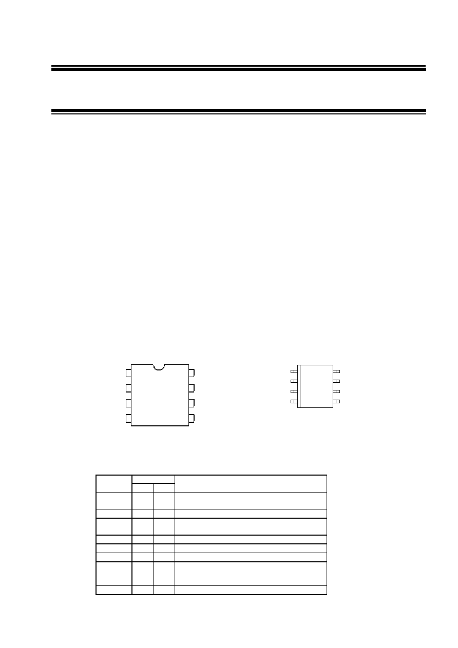
Package
8-pin DIP (PKG drawing code : DP008-A,DP008-E)
8-pin SOP (PKG drawing code : FJ008-D,FJ008-E)
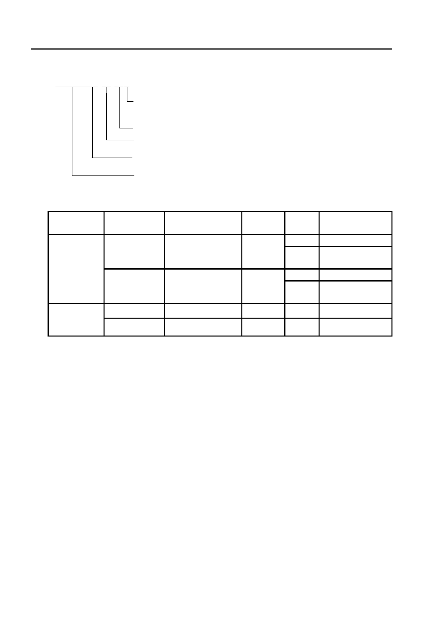
Pin Assignment
Figure 1
Pin Functions
Pin Number
Name
DIP
SOP
Function
A0
1
1
NC in the S-24C08A (no connection)*,
Connected to GND in the S-24C16A
A1
2
2
Connected to GND
A2
3
3
Address input in the S-24C08A
Connected to GND in the S-24C16A
GND
4
4
Ground
SDA
5
5
Serial data input/output
SCL
6
6
Serial clock input
WP
7
7
WP (Write Protection) pin
Connected to Vcc:
Protection valid
Connected to GND: Protection invalid
V
CC
8
8
Power supply
CMOS 2-WIRED SERIAL EEPROM
S-24C08A/16A
∑
Endurance:
10
5
cycles/word
∑
Data retention:
10 years
∑
Write protection (S-24C08A, S-24C16A)
∑
S-24C08A:
8 kbits
∑
S-24C16A:
16 kbits
*
The data sheet of 1K/2K/4K-bit products are available.
(S-24C0XA Series)
Features
∑
Low power consumption
Standby:
1.0
µ
A Max. (V
CC
=5.5 V)
Operating: 0.8 mA Max. (V
CC
=5.5 V f=400kHz)
0.4 mA Max. (V
CC
=4.5 V f=100kHz)
∑
Wide operating voltage range
Write:
2.5 to 5.5 V
Read:
1.8 to 5.5 V
∑
Page write
16 bytes (S-24C08A, S-24C16A)
∑
Sequential read capable
* When in use, connect to
GND or VCC.
8-pin DIP
Top view
V
CC
GND
SCL
A1
A2
SDA
A0
1
2
3
4
5
6
7
8
WP
S-24C08ADPA-uuw
S-24C16ADPA-uuw
8-pin SOP
Top view
A0
A1
A2
GND
WP
V
CC
SCL
SDA
3
4
1
2
6
5
8
7
S-24C08AFJA-zz-uuw
S-24C16AFJA-zz-uuw
Table 1
* Lower-case letters zz and uuw differ depending on
the packing form.
See Ordering Information and Dimensions.

CMOS 2-WIRED SERIAL EEPROM
S-24C08A/16A Series Rev. 1.3
_30
2
Seiko Instruments Inc.
Block Diagram
Absolute Maximum Ratings
Table 2
Parameter
Symbol
Ratings
Unit
Power supply voltage
V
CC
-0.3 to +7.0
V
Input voltage
V
IN
-0.3 to V
CC
+0.3
V
Output voltage
V
OUT
-0.3 to V
CC
V
Storage temperature under bias
T
bias
-50 to +95
∞C
Storage temperature
T
stg
-65 to +150
∞C
Figure 2
V
CC
GND
Serial Clock
Controller
Device Address
Comparator
Address
Counter
Y Decoder
Data Output
ACK Output
Controller
High-Voltage Generator
Start/Stop
Detector
Data Register
EEPROM
X
Decoder
Selector
SCL
SDA
A2*
D
IN
D
OUT
R / W
LOA
IN
COMP
LOAD
WP
*
S-24C08A

CMOS 2-WIRED SERIAL EEPROM
Rev. 1.3
_30
S-24C08A/16A Series
Seiko Instruments Inc.
3
Recommended Operating Conditions
Table 3
Parameter
Symbol
Conditions
Min.
Typ.
Max.
Unit
Read Operation
1.8
--
5.5
V
Power supply voltage
V
CC
Write Operation
2.5
--
5.5
V
V
CC
=2.5 to 5.5V
0.7
◊V
CC
--
V
CC
V
High level input voltage
V
IH
V
CC
=1.8 to 2.5V
0.8
◊V
CC
--
V
CC
V
V
CC
=2.5 to 5.5V
0.0
--
0.3
◊V
CC
V
Low level input voltage
V
IL
V
CC
=1.8 to 2.5V
0.0
--
0.2
◊V
CC
V
Operating temperature
T
opr
--
-40
--
+85
∞C
Pin Capacitance
Table 4
(Ta=25∞C, f=1.0 MHz, V
CC
=5 V)
Parameter
Symbol
Conditions
Min.
Typ.
Max.
Unit
Input capacitance
C
IN
V
IN
=0 V (SCL, A0, A1, A2, WP)
--
--
10
pF
Input/output capacitance
C
I / O
V
I / O
=0 V (SDA)
--
--
10
pF
Endurance
Table 5
Parameter
Symbol
Min.
Typ.
Max.
Unit
Endurance
N
W
10
5
--
--
cycles/word
CMOS 2-WIRED SERIAL EEPROM
S-24C08A/16A Series Rev. 1.3
_30
4
Seiko Instruments Inc.
DC Electrical Characteristics
Table 6
V
CC
=4.5 V to 5.5
V
V
CC
=2.5 to 4.5
V
V
CC
=1.8 to 2.5 V
Parameter
Symbol
Min.
Typ.
Max.
Min.
Typ.
Max.
Min.
Typ.
Max.
Unit
Current consumption
(READ)
I
CC1
--
--
0.8
f=400kHz
--
--
0.4
f=100kHz
--
--
0.3
f=100kHz
mA
Current consumption
(PROGRAM)
I
CC2
--
--
4.0
f=400kHz
--
--
3.5
f=100kHz
--
--
--
mA
Table 7
V
CC
=4.5 V to 5.5 V
V
CC
=2.5 to 4.5 V
V
CC
=1.8 to 2.5 V
Parameter
Symbol
Conditions
Min.
Typ.
Max.
Min.
Typ.
Max.
Min.
Typ.
Max.
Unit
Standby current
consumption
I
SB
V
IN
=V
CC
or GND
--
--
1.0
--
--
0.6
--
--
0.4
µA
Input leakage
current
I
LI
V
IN
=GND to V
CC
--
0.1
1.0
--
0.1
1.0
--
0.1
1.0
µA
Output leakage
current
I
LO
V
OUT
=GND to V
CC
--
0.1
1.0
--
0.1
1.0
--
0.1
1.0
µA
Low level output
voltage
V
OL
I
OL
=3.2 mA
I
OL
=1.5 mA
I
OL
=100
µA
--
--
--
--
--
--
0.4
0.3
0.1
--
--
--
--
--
--
0.4
0.3
0.1
--
--
--
--
--
--
--
0.5
0.1
V
V
V
Current address
retention
voltage
V
AH
--
1.5
--
5.5
1.5
--
4.5
1.5
--
2.5
V
CMOS 2-WIRED SERIAL EEPROM
Rev. 1.3
_30
S-24C08A/16A Series
Seiko Instruments Inc.
5
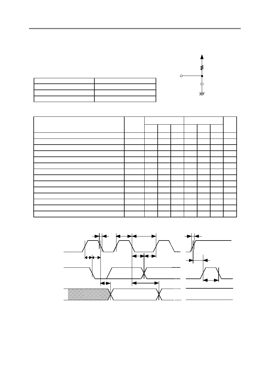
AC Electrical Characteristics
Input pulse voltage
0.1
◊V
CC
to 0.9
◊V
CC
Input pulse rising/falling time
20 ns
Output judgment voltage
0.5
◊V
CC
Output load
100 pF+ Pullup resistance 1.0 k
Table 9
V
CC
=1.8V to 5.5V
V
CC
=4.5V to 5.5V
Parameter
Symbol
Min.
Typ.
Max.
Min.
Typ.
Max.
Unit
SCL clock frequency
f
SCL
0
--
100
0
--
400
kHz
SCL clock time "L"
t
LOW
4.7
--
--
1.3
--
--
µs
SCL clock time"H"
t
HIGH
4.0
--
--
0.6
--
--
µs
SDA output delay time
t
AA
0.3
--
3.5
0.3
--
1.0
µs
SDA output hold time
t
DH
0.3
--
--
0.3
--
--
µs
Start condition setup time
t
SU.STA
4.7
--
--
0.6
--
--
µs
Start condition hold time
t
HD.STA
4.0
--
--
0.6
--
--
µs
Data input setup time
t
SU.DAT
100
--
--
50
--
--
ns
Data input hold time
t
HD.DAT
0
--
--
0
--
--
ns
Stop condition setup time
t
SU.STO
4.7
--
--
0.6
--
--
µs
SCL ∑ SDA rising time
t
R
--
--
1.0
--
--
0.3
µs
SCL ∑ SDA falling time
t
F
--
--
0.3
--
--
0.3
µs
Bus release time
t
BUF
4.7
--
--
1.3
--
--
µs
Noise suppression time
t
I
--
--
100
--
--
100
ns
Table 8
Measurement Conditions
Figure 4
Bus Timing
SCL
SDA IN
SDA OUT
t
BUF
t
R
t
SU.STO
t
SU.DAT
t
HD.DAT
t
DH
t
AA
t
HIGH
t
LOW
t
HD.STA
t
SU.STA
t
F
V
CC
R=1.0k
SDA
C=100pF
Figure 3
Output Load Circuit

CMOS 2-WIRED SERIAL EEPROM
S-24C08A/16A Series Rev. 1.3
_30
6
Seiko Instruments Inc.
Table 10
V
CC
=4.5 to 5.5V
V
CC
=2.5 to 4.5V
Item
Symbol
Min.
Typ.
Max.
Min.
Typ.
Max.
Unit
Write time
t
WR
--
0.8
1.0
--
4.0
5.0
ms
Pin Functions
1. Address Input Pins (A2)
Connect pins A2 to the GND or the V
CC
to assign slave addresses. There are 2 different ways to assign
slave addresses in the S-24C08A. The S-24C16A doesn't have address input, so the slave address
cannot be input. When the input slave address coincides with the slave address transmitted from the
master device, 1 device can be selected from among multiple devices connected to the bus. Always
connect the address input pin to GND or V
CC
and leave it unchanged.
2. SDA (Serial Data Input/Output) Pin
The SDA pin is used for bilateral transmission of serial data. It consists of a signal input pin and an Nch
open-drain transistor output pin.
Usually pull up the SDA line via resistance to the V
CC
, and use it with other open-drain or open-collector
output devices connected in a wired OR configuration.
3. SCL (Serial Clock Input) Pin
The SCL pin is used for serial clock input. It is capable of processing signals at the rising and falling edges
of the SCL clock input signal. Make sure the rising time and falling time conform to the specifications.
4. WP Pin
In the S-24C08A and the S-24C16A, this pin is used for write protection. When there is no need for write
protection, connect the pin to the GND; when there is a need for write protection, connect the pin to the
Vcc.
Figure 5
Write Cycle
SCL
SDA
D0
Write data
Acknowledge
Stop
condition
Start
condition
t
WR
CMOS 2-WIRED SERIAL EEPROM
Rev. 1.3
_30
S-24C08A/16A Series
Seiko Instruments Inc.
7
Operation
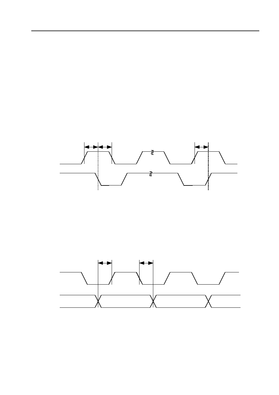
1. Start Condition
When the SCL line is "H," the SDA line changes from "H" to "L." This allows the device to go to the start
condition.
All operations begin from the start condition.
2. Stop Condition
When the SCL line is "H," the SDA line changes from "L" to "H." This allows the device to go to the stop
condition.
When the device receives the stop condition signal during a read sequence, the read operation is
interrupted, and the device goes to standby mode.
When the device receives the stop condition signal during write sequence, the retrieval of write data is
halted, and the EEPROM initiates rewrite
.
3. Data Transmission
Changing the SDA line while the SCL line is "L" allows the data to be transmitted. A start or stop condition
is recognized when the SDA line changes while the SCL line is "H."
Figure 6
Start/Stop Conditions
t
SU.STA
t
HD.STA
t
SU.STO
Start
Condition
Stop
Condition
SCL
SDA
Figure 7
Data Transmission Timing
t
SU.DAT
t
HD.DAT
SCL
SDA

CMOS 2-WIRED SERIAL EEPROM
S-24C08A/16A Series Rev. 1.3
_30
8
Seiko Instruments Inc.
4. Acknowledgment
The unit of data transmission is 8 bits. By turning the SDA line "L," the slave device mounted on the
system bus which receives the data during the 9th clock cycle outputs the acknowledgment signal
verifying the data reception.
When the EEPROM is rewriting, the device does not output the acknowledgment signal.
5. Device Addressing
To perform data communications, the master device mounted on the system outputs the start condition
signal to the slave device.
Next, the master device outputs 7-bit length device address and a 1-bit length
read/write instruction code onto the SDA bus.
Upper 4 bits of the device address are called the "Device Code," and set to "1010." Successive 3 bits (P2, P1, P0)
are called the "Page Address." (In the S-24C08A, P2 is Slave Address A2.) Any of memory blocks (the S-24C08A
has four 256-byte memory blocks and the S-24C16A has eight 256-byte memory blocks) can be selected at P2, P1,
and P0.
Figure 8 Acknowledgment Output Timing
1
8
9
Acknow-
ledgment
Output
t
AA
t
DH
Start
Condition
SCL
(EEPROM Input)
SDA
(Master Output)
SDA
(EEPROM Output)
Figure 9
Device Address
Page Address
1
0
1
0
A2
P1
P0
R/W
Device Code
S-24C08A
S-24C16A
MSB
LSB
1
0
1
0
P2
P1
P0
R/W
CMOS 2-WIRED SERIAL EEPROM
Rev. 1.3
_30
S-24C08A/16A Series
Seiko Instruments Inc.
9
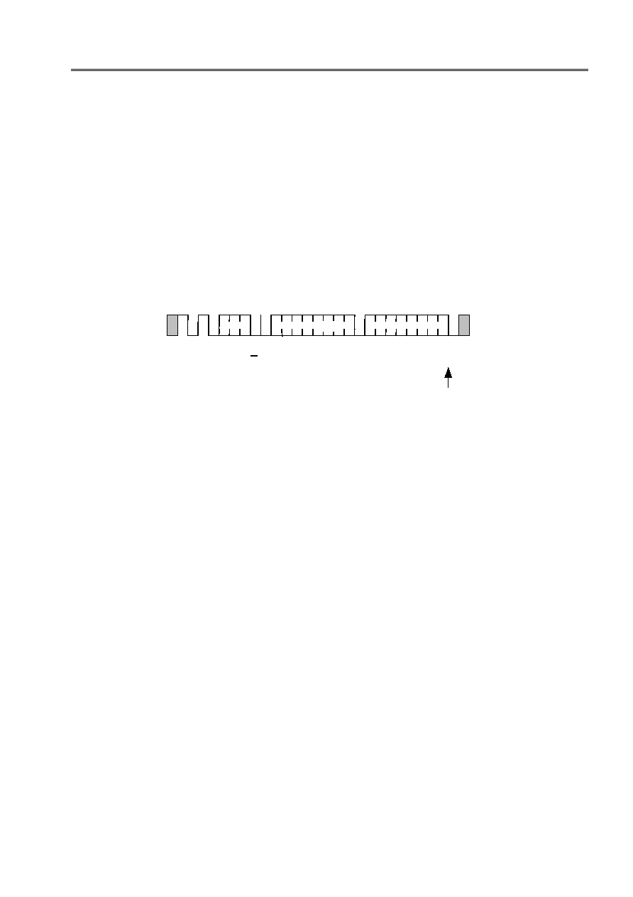
6. Write
6.1 Byte Write
When the EEPROM receives a 7-bit length device address and a 1-bit read/write instruction code
"0," following the start condition signal, it outputs the acknowledgment signal. Next, when the
EEPROM receives an 8-bit length word address, it outputs the acknowledgment signal.
After the EEPROM receives 8-bit write data and outputs the acknowledgment signal, it receives the
stop condition signal. Next, the EEPROM at the specified memory address starts to rewrite.
When the EEPROM is rewriting, all operations are prohibited and the acknowledgment signal is not
output.
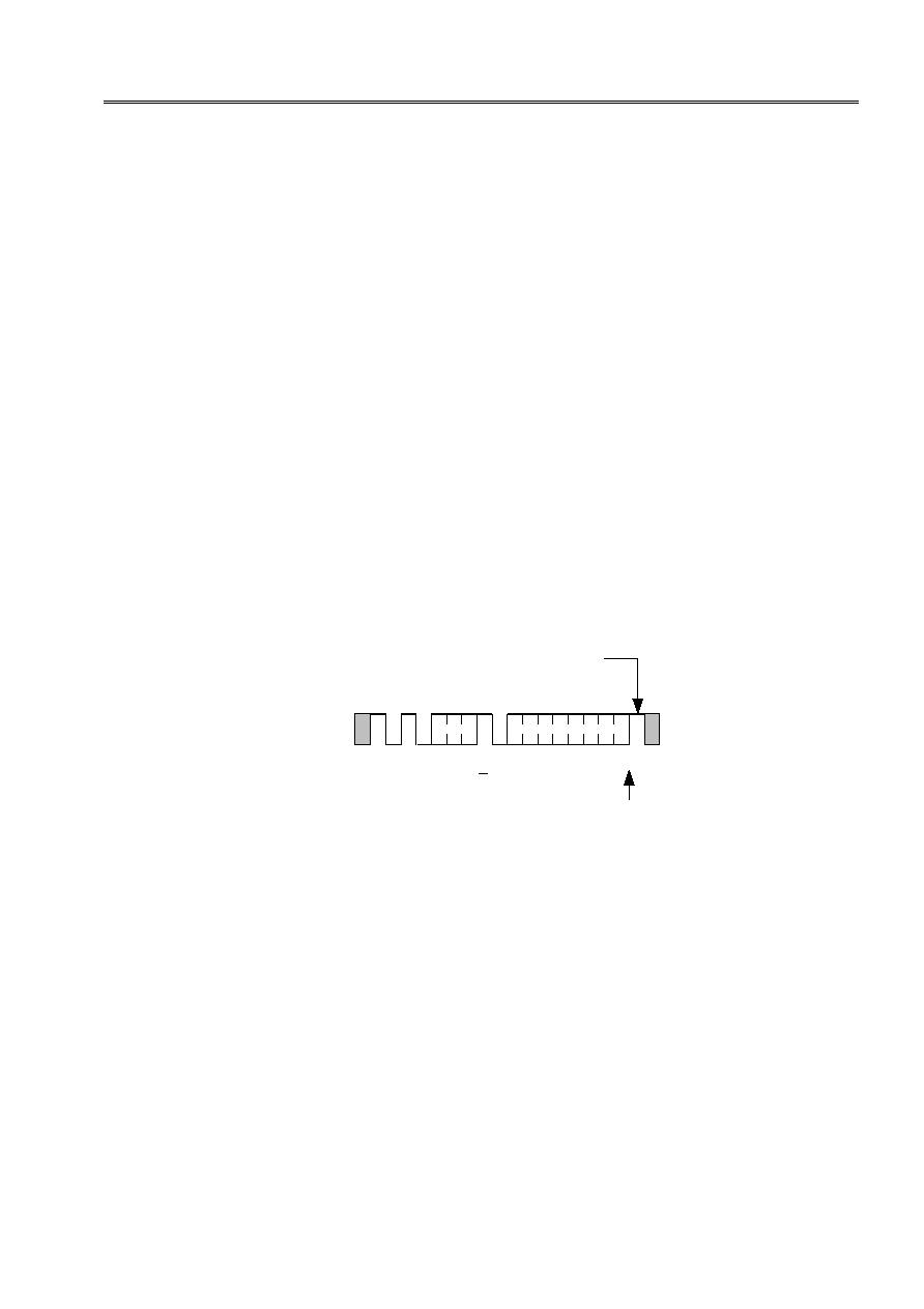
6.2 Page Write
Up to 16 bytes per page can be written in the S-24C08A and S-24C16A.
Basic data transmission procedures are the same as those in the "Byte Write." However, when the
EEPROM receives 8-bit write data which corresponds to the page size, the page can be written.
When the EEPROM receives a 7-bit length device address and a 1-bit read/write instruction code
"0," following the start condition signal, it outputs the acknowledgment signal. When the EEPROM
receives an 8-bit length word address, it outputs the acknowledgment signal.
After the EEPROM receives 8-bit write data and outputs the acknowledgment signal, it receives 8-
bit write data corresponding to the next word address, and outputs the acknowledgment signal. The
EEPROM repeats reception of 8-bit write data and output of the acknowledgment signal in
succession. It is capable of receiving write data corresponding to the maximum page size.
When the EEPROM receives the stop condition signal, it starts to rewrite, corresponding to the size
of the page, on which write data, starting from the specified memory address, is received.
Figure 10
Byte Write
S
T
A
R
T
1 0 1 0
W
R
I
T
E
S
T
O
P
DEVICE
ADDRESS
WORD ADDRESS
DATA
R
/
W
M
S
B
SDA LINE
ADR INC (ADDRESS INCREMENT)
P2 P1 P0
W7W6W5W4W3W2W1W0
D7 D6 D5 D4 D3 D2 D1 D0
A
C
K
L
S
B
A
C
K
A
C
K
0
(
P2 is A2 in the S-24C08A.)

CMOS 2-WIRED SERIAL EEPROM
S-24C08A/16A Series Rev. 1.3
_30
10
Seiko Instruments Inc.
Figure 11
Page Write
In the S-24C08A or S-24C16A, the lower 4 bits at the word address are automatically incremented
each when the EEPROM receives 8 bit write data.
Even when the write data exceeds 16 bytes, the upper 4 bits of the word address and page address
(P2, P1, P0) remain unchanged, and the lower 4 bits are rolled over and overwritten.
6.3 Acknowledgment Polling
Acknowledgment polling is used to know when the rewriting of the EEPROM is finished.
After the EEPROM receives the stop condition signal and once it starts to rewrite, all operations are
prohibited. Also, the EEPROM cannot respond to the signal transmitted by the master device.
Accordingly, the master device transmits the start condition signal and the device address read/write
instruction code to the EEPROM (namely, the slave device) to detect the response of the slave
device. This allows users to know when the rewriting of the EEPROM is finished.
That is, if the slave device does not output the acknowledgment signal, it means that the EEPROM is
rewriting; when the slave device outputs the acknowledgment signal, you can know that rewriting
has been completed. It is recommended to use read instruction "1" for the read/write instruction
code transmitted by the master device.
6.4 Write Protection
The S-24C08A and the S-24C16A are capable of protecting the memory. When the WP pin is
connected to V
CC
, writing to all memory area is prohibited.
When the WP pin is connected to GND, the write protection becomes invalid, and writing in all
memory area becomes available. However, when there is no need for using write protection, always
connect the WP pin to GND.
S
T
A
R
T
1 0 1 0
W
R
I
T
E
S
T
O
P
DEVICE
ADDRESS
WORD ADDRESS (n)
DATA (n)
R
/
W
M
S
B
SDA LINE
ADR INC
P2 P1 P0
W7W6W5W4W3W2W1W0
D7 D6 D5 D4 D3 D2 D1 D0
A
C
K
L
S
B
A
C
K
A
C
K
0
D7
D0
D7
D0
ADR INC
A
C
K
ADR INC
A
C
K
DATA (n+1)
DATA (n+x)
(P2 is A2 in the S-24C08A.)
CMOS 2-WIRED SERIAL EEPROM
Rev. 1.3
_30
S-24C08A/16A Series
Seiko Instruments Inc.
11
7.
Read
7.1 Current Address Read
The EEPROM is capable of storing the last accessed memory address during both writing and
reading. The memory address is stored as long as the power voltage is more than the retention
voltage V
AH
.
Accordingly, when the master device recognizes the position of the address pointer inside the
EEPROM, data can be read from the memory address of the current address pointer without
assigning a word address. This is called"Current Address Read"
"Current Address Rea" is explained for when the address counter inside the EEPROM is an "n"
address.
When the EEPROM receives a 7-bit length device address and a 1-bit read/write instruction code
"1," following the start condition signal, it outputs the acknowledgment signal. However, in the S-
24C08A/16A, page address (P1, P0)/(P2, P1, P0) becomes invalid, and the memory address of the
current address pointer becomes valid.
Next, 8-bit length data at an "n" address is output from the EEPROM, in synchronization with the
SCL clock.
The address counter is incremented at the falling edge of the SCL clock by which the 8th bit of data
is output, and the address counter goes to address n+1.
The master device does not output the acknowledgment signal and transmits the stop condition
signal to finish reading
.
For recognition of the address pointer inside the EEPROM, take into consideration the following:
The memory address counter inside the EEPROM is automatically incremented for every falling edge of the SCL
clock by which the 8th bit of data is output during the time of reading. During the time of writing, upper bits
of the memory address (upper 4 bits of the word address and page address) are left unchanged and are
not incremented.
Figure 12
Current Address Read
S
T
A
R
T
1 0 1 0
R
E
A
D
S
T
O
P
DEVICE
ADDRESS
R
/
W
M
S
B
SDA LINE
ADR INC
P2 P1 P0
D7 D6 D5 D4 D3 D2 D1 D0
A
C
K
L
S
B
1
DATA
NO ACK from
Master Device
(P2 is A2 in the S-24C08A)

CMOS 2-WIRED SERIAL EEPROM
S-24C08A/16A Series Rev. 1.3
_30
12
Seiko Instruments Inc.
7.2 Random Read
Random read is a mode used when the data is read from arbitrary memory addresses.
To load a memory address into the address counter inside the EEPROM, first perform a dummy write according to
the following procedures:
When the EEPROM receives a 7-bit length device address and a 1-bit read/write instruction code
"0," following the start condition signal, it outputs the acknowledgment signal.
Next, the EEPROM receives an 8-bit length word address and outputs the acknowledgment signal.
Last, the memory address is loaded into the address counter of the EEPROM.
the EEPROM receives the write data during byte or page writing. However, data reception is not performed during
dummy write.
The memory address is loaded into the memory address counter inside the EEPROM during dummy
write. After that, the master device can read the data starting from the arbitrary memory address by
transmitting a new start condition signal and performing the same operation as that in the "Current
Read."
That is, when the EEPROM receives a 7-bit length device address and a 1-bit read/write instruction
code "1," following the start condition signal, it outputs the acknowledgment signal.
Next, 8-bit length data is output from the EEPROM, in synchronization with the SCL clock. The
master device does not output an acknowledgment signal and transmits the stop condition signal to
finish reading.
Figure 13 Random Read
S
T
A
R
T
1 0 1 0
W
R
I
T
E
S
T
O
P
DEVICE
ADDRESS
WORD ADDRESS (n)
R
/
W
M
S
B
SDA LINE
P2 P1 P0
W7W6W5W4W3W2W1W0
A
C
K
L
S
B
A
C
K
A
C
K
0
1 0 1 0 P2 P1 P0 1
D7 D6 D5 D4 D3 D2 D1 D0
DATA (n)
DUMMY WRITE
DEVICE
ADDRESS
R
E
A
D
NO ACK from
Master Device
ADR INC
S
T
A
R
T
(P2 is A2 in the S-24C08A.)

CMOS 2-WIRED SERIAL EEPROM
Rev. 1.3
_30
S-24C08A/16A Series
Seiko Instruments Inc.
13
7.3 Sequential Read
When the EEPROM receives a 7-bit length device address and a 1-bit read/write instruction code "1" in
both current and random read operations, following the start condition signal, it outputs the
acknowledgment signal
When 8-bit length data is output from the EEPROM, in synchronization with the SCL clock, the memory address
counter inside the EEPROM is automatically incremented at the falling edge of the SCL clock, by which
the 8th data is output.
When the master device transmits the acknowledgment signal, the next memory address data is output.
When the master device transmits the acknowledgment signal, the memory address counter inside the
EEPROM is incremented and read data in succession. This is called "Sequential Read."
When the master device does not output an acknowledgement signal and transmits the stop condition
signal, the read operation is finished.
Data can be read in the "Sequential Read" mode in succession. When the memory address counter
reaches the last word address, it rolls over to the first memory address.
Figure 14
Sequential Read
R
E
A
D
S
T
O
P
DEVICE
ADDRESS
R
/
W
ADR INC
D7
D0
A
C
K
A
C
K
A
C
K
1
D7
D0
ADR INC
A
C
K
ADR INC
SDA LINE
DATA (n)
D7
D0
D7
D0
DATA (n+1)
DATA (n+2)
DATA (n+x)
NO ACK from
Master Device
ADR INC

CMOS 2-WIRED SERIAL EEPROM
S-24C08A/16A Series Rev. 1.3
_30
14
Seiko Instruments Inc.
8. Address Increment Timing
The address increment timing is as follows. See Figures 15 and 16. During reading operation, the memory
address counter is automatically incremented at the falling edge of the SCL clock (the 8th read data is
output).
During writing operation, the memory address counter is also automatically incremented at the
falling edge of the SCL clock when the 8th bit write data is fetched.
Figure 15
Address Increment Timing During Reading
SCL
SDA
R / W=1
Address Increment
8
9
1
8
9
D7 Output
D0 Output
ACK Output
Figure 16
Address Increment Timing During Writing
SCL
SDA
R / W=0
8
9
1
8
9
D7 Input
D0 Input
ACK Output
ACK Output
Address Increment
Purchase of I
2
C components of Seiko Instruments Inc. conveys a license under the Philips I
2
C
Patent Rights to use these components in an I
2
C system, provided that the system conforms to the
I
2
C Standard Specification as defined by Philips.
Please note that any product or system incorporating this IC may infringe upon the Philips I
2
C Bus
Patent Rights depending upon its configuration.
In the event that such product or system incorporating the I
2
C Bus infringes upon the Philips Patent
Rights, Seiko Instruments Inc. shall not bear any responsibility for any matters with regard to and
arising from such patent infringement.

CMOS 2-WIRED SERIAL EEPROM
Rev. 1.3
_30
S-24C08A/16A Series
Seiko Instruments Inc.
15
Characteristics
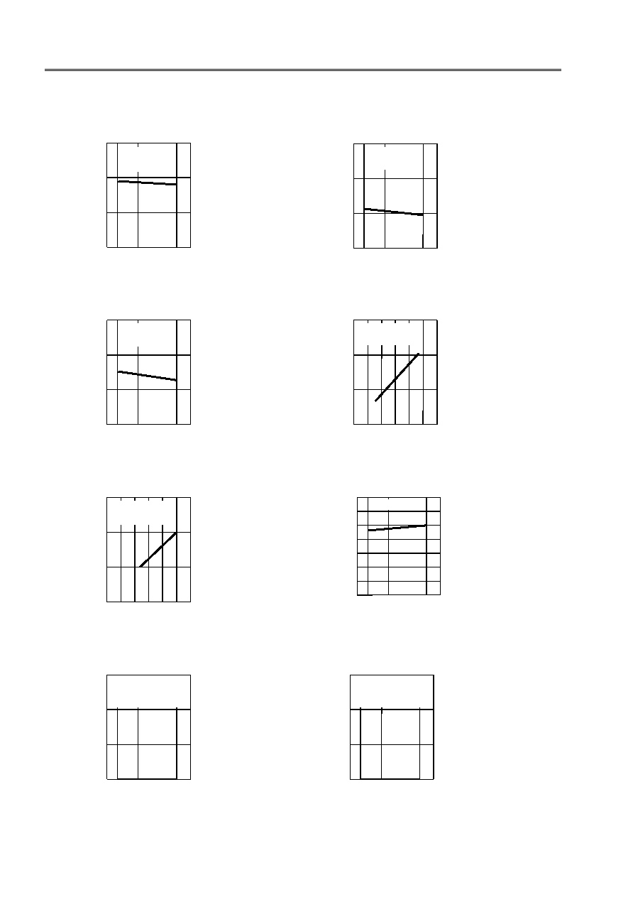
1. DC Characteristics
1.3 Current consumption (READ) I
CC1
--
Ambient temperature Ta
1.1 Current consumption (READ) I
CC1
--
Ambient temperature Ta
Ta (∞C)
200
100
V
CC
=5.5 V
fscl=100 KHz
DATA=0101
0
-40
0
85
I
CC1
(uA)
Ta (∞C)
200
100
V
CC
=3.3 V
fscl=100 KHz
DATA=0101
0
-40
0
85
I
CC1
(uA)
1.2 Current consumption (READ) I
CC1
--
Ambient temperature Ta
Ta (∞C)
400
200
V
CC
=5.5 V
fscl=400 KHz
DATA=0101
0
-40
0
85
I
CC1
(uA)
1.4 Current consumption (READ) I
CC1
--
Ambient temperature Ta
Ta (∞C)
60
40
V
CC
=1.8 V
fscl=100 KHz
DATA=0101
0
-40
0
85
I
CC1
(uA)
1.5 Current consumption (READ) I
CC1
--
Power supply voltage V
CC
200
100
0
2 3 4
5 6
7
Ta=25∞C
fscl=100 KHz
V
CC
(V)
I
CC1
(uA)
1.6 Current consumption (READ) I
CC1
--
Power supply voltage V
CC
400
200
0
2 3 4 5 6
7
Ta=25∞C
fscl=400 KHz
V
CC
(V)
I
CC1
(uA)
1.7 Current consumption (READ) I
CC1
-
Clock frequency
fscl
400
200
0
I
CC1
(
µ
A)
V
CC
=5.0 V
Ta=25∞C
100K 200K
fscl(Hz)
300K 400K
1.8 Current consumption (PROGRAM) I
CC2
--
Ambient temperature Ta
Ta (∞C)
1.0
0.5
V
CC
=5.5 V
fscl=100 KHz
0
-40
0
85
I
CC2
(mA)
CMOS 2-WIRED SERIAL EEPROM
S-24C08A/16A Series Rev. 1.3
_30
16
Seiko Instruments Inc.
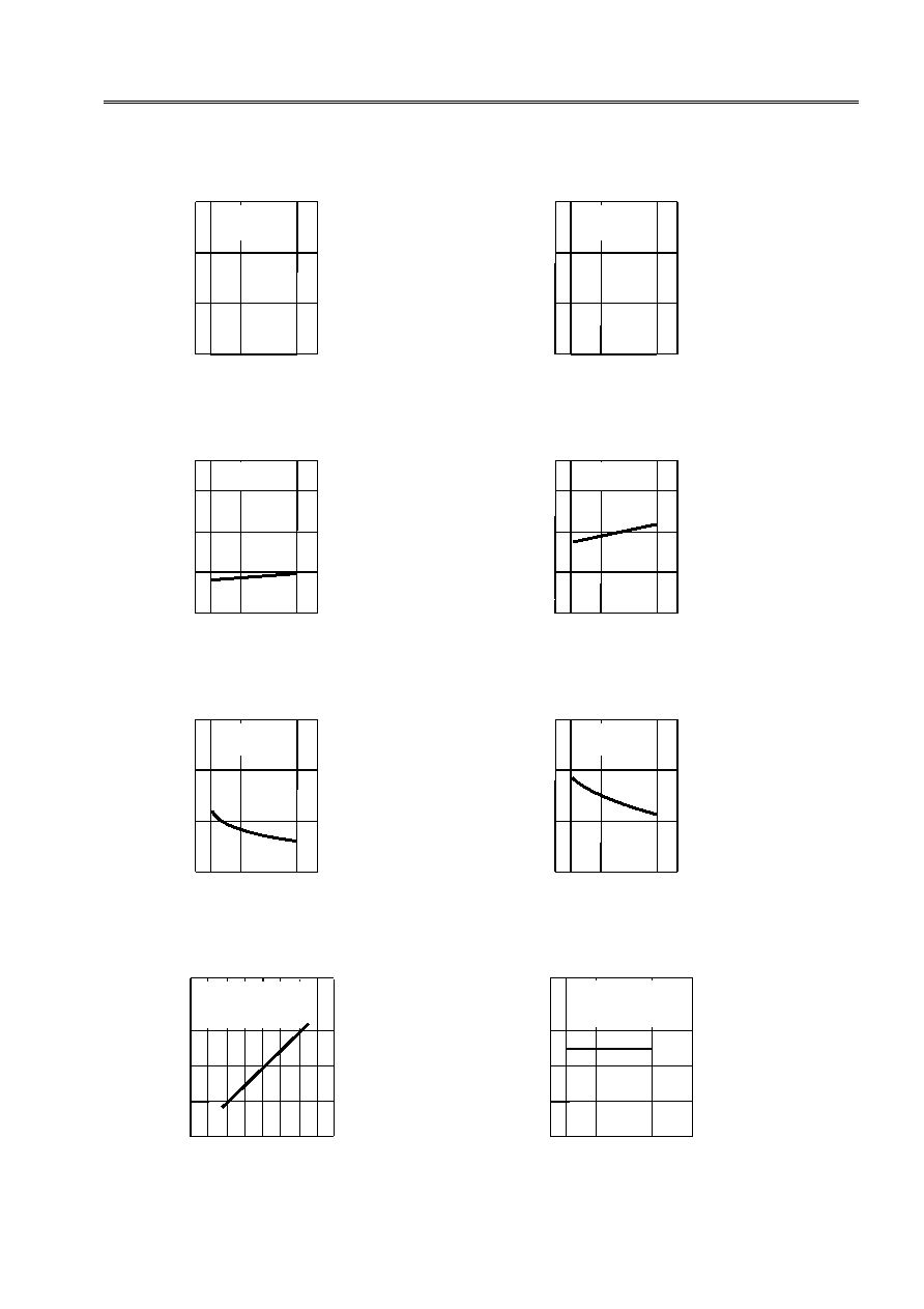
1.9 Current consumption (PROGRAM) I
CC2
--
Ambient temperature Ta
Ta (∞C)
3.0
1.5
V
CC
=5.5 V
fscl=400 KHz
0
-40
0
85
I
CC2
(mA)
1.10 Current consumption (PROGRAM) I
CC2
--
Ambient temperature Ta
Ta (∞C)
1.0
0.5
V
CC
=3.3 V
fscl=100 KHz
0
-40
0
85
I
CC2
(mA)
1.11 Current consumption (PROGRAM) I
CC2
--
Ambient temperature Ta
Ta (∞C)
1.0
0.5
V
CC
=2.5 V
fscl=100 KHz
0
-40
0
85
I
CC2
(mA)
1.12 Current consumption (PROGRAM) I
CC2
--
Power supply voltage V
CC
1.0
0.5
0
2 3 4 5 6
7
Ta=25∞C
fscl=100
KHz
V
CC
(V)
I
CC2
(mA)
1.13 Current consumption (PROGRAM) I
CC2
--
Power supply voltage V
CC
3.0
1.5
0
2 3 4 5 6
7
Ta=
25∞C
fscl=400
V
CC
(V)
I
CC2
(mA)
1.14 Standby current consumption I
SB
--
Ambient temperature Ta
10
-6
10
-7
10
-8
10
-9
10
-10
V
CC
=5.5 V
10
-11
Ta (∞C)
-40
0
85
I
SB
(A)
1.15 Input leakage current I
LI
--
Ambient temperature Ta
Ta (∞C)
1.0
0.5
V
CC
=5.5 V
A0, A1, A2, SDA
SCL,TEST/WP=0V
0
-40
0
85
I
LI
(
µ
A)
1.16 Input leakage current I
LI
--
Ambient temperature Ta
Ta (∞C)
1.0
0.5
0
-40
0
85
V
CC
=5.5 V
A0, A1, A2, SDA
SCL,TEST/WP=5.5
I
LI
(
µ
A)
CMOS 2-WIRED SERIAL EEPROM
Rev. 1.3
_30
S-24C08A/16A Series
Seiko Instruments Inc.
17
1.17 Output leakage current I
LO
--
Ambient temperature Ta
Ta (∞C)
1.0
0.5
V
CC
=5.5 V
SDA=0V
0
-40
0
85
I
LO
(
µ
A)
1.18 Output leakage current I
LO
--
Ambient temperature Ta
Ta (∞C)
1.0
0.5
V
CC
=5.5 V
SDA=5.5 V
0
-40
0
85
I
LO
(
µ
A)
1.19 Low level output voltage V
OL
--
Ambient temperature Ta
Ta (∞C)
0.3
0.2
V
CC
=4.5 V
I
OL
=2.3 mA
-40
0
85
V
OL
(V)
0.1
1.20 Low level output voltage V
OL
--
Ambient temperature Ta
Ta (∞C)
0.03
0.02
V
CC
=1.8 V
I
OL
=100
µ
A
-40
0
85
V
OL
(V)
0.01
1.21 Low level output current I
OL
--
Ambient temperature Ta
Ta (∞C)
20
10
V
CC
=4.5 V
V
OL
=0.45 V
0
-40
0
85
I
OL
(mA)
1.22 Low level output current I
OL
--
Ambient temperature Ta
Ta (∞C)
1.0
0.5
V
CC
=1.8 V
V
OL
=0.1 V
0
-40
0
85
I
OL
(mA)
Ta=25∞C
A0, A1, A2, SDA
SCL, TEST/WP
1.0
0
2.0
3.0
VIH
(V)
1 2 3 4 5 6 7
V
CC
(V)
1.23 High input inversion voltage VIH
--
Power supply voltageV
CC
V
CC
=5.0 V
A0, A1, A2, SDA
SCL, TEST/WP
1.0
0
2.0
3.0
VIH
(V)
Ta (∞C)
1.24 High input inversion voltage VIH
--
Ambient temperature Ta
-40
0
85

CMOS 2-WIRED SERIAL EEPROM
S-24C08A/16A Series Rev. 1.3
_30
18
Seiko Instruments Inc.
Ta=25∞C
A0, A1, A2,SDA
1.0
0
2.0
3.0
VIL
(V)
1 2 3 4 5 6 7
V
CC
(V)
1.25 Low input inversion voltage VIL
--
Power supply voltageV
CC
1.0
0
2.0
3.0
VIL
(V)
Ta (∞C)
1.26 Low input inversion voltage VIL
--
Ambient temperature Ta
-40
0
85
Ta=5.0V
A0, A1, A2,SDA
SCL, TEST/WP

CMOS 2-WIRED SERIAL EEPROM
Rev. 1.3
_30
S-24C08A/16A Series
Seiko Instruments Inc.
19
2. AC Characteristics
2.2
Write time t
WR
--
Power supply voltage V
CC
2.1
Maximum operating frequency f
max
--
Power supply voltage V
CC
2.4
Write time t
WR
--
Ambient temperature Ta
2.3
Write time t
WR
--
Ambient temperature Ta
10K
2 3 4
5
Ta=25∞C
V
CC
(V)
f
max
(Hz)
1
2
2 3 4 5 6
7
Ta=25∞C
V
CC
(V)
t
WR
(ms)
1
100K
1M
Ta (∞C)
1.5
1.0
V
CC
=4.5 V
-40
0
85
0.5
t
WR
(ms)
Ta (∞C)
4
3
V
CC
=2.5 V
-40
0
85
2
t
WR
(ms)
2.6
SDA output delay time t
PD
--
Ambient temperature Ta
2.5
SDA output delay time t
PD
--
Ambient temperature Ta
Ta (∞C)
1.5
1.0
V
CC
=4.5 V
-40
0
85
0.5
t
PD
(
µ
s)
Ta (∞C)
1.5
1.0
V
CC
=2.7 V
-40
0
85
0.5
t
PD
(
µ
s)
2.7
SDA output delay time t
PD
--
Ambient temperature Ta
Ta (∞C)
3.0
2.0
V
CC
=1.8 V
-40
0
85
1.0
t
PD
(
µ
s)
1
4
3
5
CMOS 2-WIRED SERIAL EEPROM
S-24C08A/16A Series Rev. 1.3
_30
20
Seiko Instruments Inc.
Ordering Information
S-24CxxA yyy - zz - uuw
P code (Distincion for package process)
None
S
Endurance code
01
: 10
5
cycles
Taping specification
None for DIP and SOP in magazine
TB
Package code
DPA
: DIP
FJA
: SOP
Product name
S-24C08A : 8k bits
S-24C16A : 16k bits
Product name
Package code
Taping specification
Endurance
code
P code
Package/Tape/Reel
drawings
None
DP008-A
DPA
None
-01
S
DP008-A
DP008-E
None
FJ008-D
S-24C08A
FJA
-TB
(None for magazine)
-01
S
FJ008-D
FJ008-E
DPA
None
-01
None
DP008-A
S-24C16A
FJA
-TB
(None for magazine)
-01
None
FJ008-D
Note
1)
Package dimensions of SOPs whose package code is FJA are the same in the range of deviation.
2)
Please contact an SII local office or a local representative for details.

DP008-A
011129
1
4
8
5
0.5±0.1
2.54
1.0
1.5
0∞~15∞
0.3
+0.1
-0.05
7.62
9.3(9.6max)
No.:DP008-A-P-SD-1.0
n 8-Pin DIP
Unit:mm
lDimensions
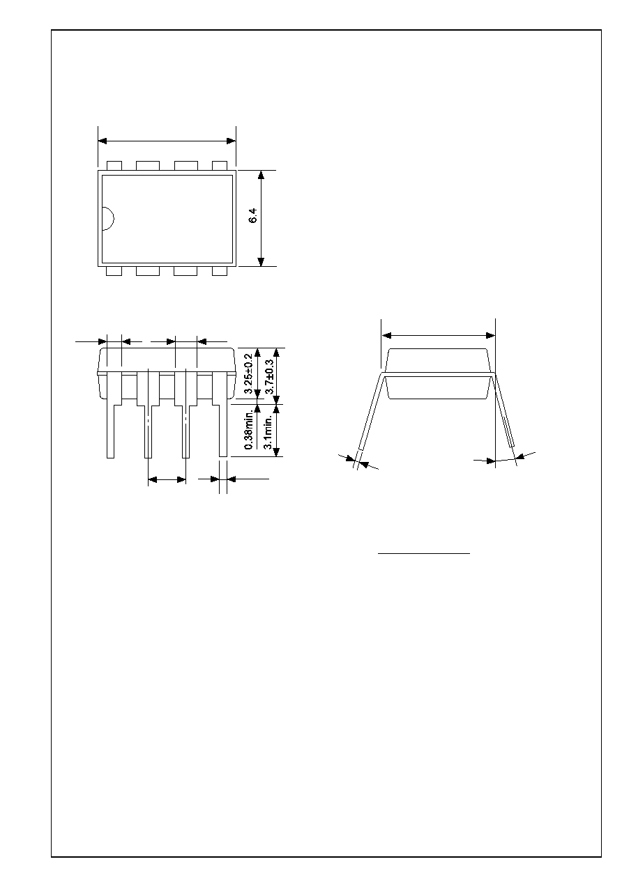
l Dimensions
n 8-Pin DIP
DP008-E
Rev.1.0
0111203
Unit : mm
No. : DP008-E-P-SD-2.0
0.5±0.1
2.54
1.0
1.5
0.25±0.05
7.62
9.3(9.6max.)
1
4
5
8
0∞ to 15∞

l Reel Specifications
l Tape Specifications
l Dimensions
n 8-Pin SOP
Unit : mm
¯2.0±0.05
¯1.55±0.05
4.0±0.1(10-pitches : total 40.0±0.2)
0.3±0.05
2.1±0.1
8.0±0.1
5∞max.
6.7±0.1
2.0±0.05
No. FJ008-D-R-SD-1 0
No. : FJ008-D-C-SD-1.0
0.4±0.05
1.27
1
4
8
5
No. : FJ008-A-P-SD-2.0
5.02±0.2
0.20±0.05
5
8
1
4
TB
Feed direction
2±0.5
13.5±0.5
60∞
2±0.5
¯13±0.2
¯21±0.8
Winding core
2000 pcs./reel
FJ008-D
Rev.1.0
011129

5
8
1
4
TB
Feed direction
l Reel Specifications
l Tape Specifications
l Dimensions
n 8-Pin SOP
FJ008-E
011204
Unit : mm
2000 pcs./reel
No.: FJ008-A-P-SD-2.0
¯1.6
¯1.5
0.3±0.05
2.1±0.1
8.0±0.1
6.4±0.1
2.0±0.05
+0.1
-0.0
+1.0
-0.1
5∞max.
4.0±0.1(10 pitches : total 40.0±0.2)
5.02±0.2
1
4
8
5
0.4±0.05
1.27
0.20±0.05
No.: FJ008-E-C-SD-1.0
No.: FJ008-E-R-SD-1.0
2±0.5
¯13
¯20.2min.
+0.5
-0.2
12.8
18.2
+0.6
-0.4
+0.6
-0.4
Winding core

∑
The information described herein is subject to change without notice.
∑
Seiko Instruments Inc. is not responsible for any problems caused by circuits or diagrams described herein
whose related industrial properties, patents, or other rights belong to third parties. The application circuit
examples explain typical applications of the products, and do not guarantee the success of any specific
mass-production design.
∑
When the products described herein are regulated products subject to the Wassenaar Arrangement or other
agreements, they may not be exported without authorization from the appropriate governmental authority.
∑
Use of the information described herein for other purposes and/or reproduction or copying without the
express permission of Seiko Instruments Inc. is strictly prohibited.
∑
The products described herein cannot be used as part of any device or equipment affecting the human
body, such as exercise equipment, medical equipment, security systems, gas equipment, or any apparatus
installed in airplanes and other vehicles, without prior written permission of Seiko Instruments Inc.
∑
Although Seiko Instruments Inc. exerts the greatest possible effort to ensure high quality and reliability, the
failure or malfunction of semiconductor products may occur. The user of these products should therefore
give thorough consideration to safety design, including redundancy, fire-prevention measures, and
malfunction prevention, to prevent any accidents, fires, or community damage that may ensue.