Document Outline
- S-24CS01A/02A/04A/08A
- Cover
- Features
- Packages
- Pin Assignments
- Block diagram
- Absolute Maximum Ratings
- Recommended Operating Conditions
- Pin Capacitance
- Endurance
- DC Electrical Characteristics
- AC Electrical Characteristics
- Pin Functions
- Operation
- Write inhibition function at low power voltage
- Precautions
- I 2 C Bus License
- Typical Characteristics
- Ordering Information
- PKG Drawings
- 8-Pin DIP
- 8-Pin SOP(JEDEC)
- 8-Pin TSSOP
Rev.2.0
_10
2-WIRE CMOS SERIAL E
2
PROM
S-24CS01A/02A/04A/08A
Seiko Instruments Inc.
1
The S-24CS01A/02A/04A/08A is a 2-wired, low power
and wide range operation 1k bit, 2k bit, 4k bit and 8k
bit E
2
PROM organized as 128 words
◊ 8 bits, 256
words
◊ 8 bits, 512 words ◊ 8 bits and 1024 words ◊
8 bits in each.
Page write and sequential read are available.
Features
∑ Low power consumption Standby : 2.0 µA Max. (V
CC
=5.5 V)
Read :
0.8 mA Max. (V
CC
=5.5 V)
∑ Operating voltage range Read :
1.8 to 5.5 V (at
-40 to +85∞C)
Write :
2.7 to 5.5 V (at
-40 to +85∞C)
∑ Page write :
8 bytes / page (S-24CS01A/02A)
16 bytes / page (S-24CS04A/08A)
∑ Sequential read
∑ Operating Frequency :
400 kHz (V
CC
=5 V
±10 %, at -40 to +85∞C)
∑ Write disable function when power supply voltage is low
∑ Endurance:
10
7
cycles/word (at +25∞C) write capable,
10
6
cycles/word (at +85∞C),
3
◊ 10
5
cycles/word (at +105∞C)
∑ Data retention:
10 years (after rewriting 10
6
cycles/word at +85∞C)
∑ S-24CS01A :
1k bit
∑ S-24CS02A :
2k bit
∑ S-24CS04A :
4k bit
∑ S-24CS08A :
8k bit
∑ High-temperature operation : +105∞C Max. supported
(Only
S-24CS0xAFJ-TBH)
∑ Write protection :
100 %
Packages
Package name
Drawing code
Package
Tape Reel
8-Pin DIP
DP008-F
8-Pin SOP(JEDEC)
FJ008-A
FJ008-D
FJ008-D
8-Pin TSSOP
FT008-A
FT008-D
FT008-D
Caution This product is intended to use in general electronic devices such as consumer electronics,
office equipment, and communications devices. Before using the product in medical
equipment or automobile equipment including car audio, keyless entry and engine control
unit, contact to SII is indispensable.
2-WIRE CMOS SERIAL E
2
PROM
S-24CS01A/02A/04A/08A
Rev.2.0
_10
Seiko Instruments Inc.
2
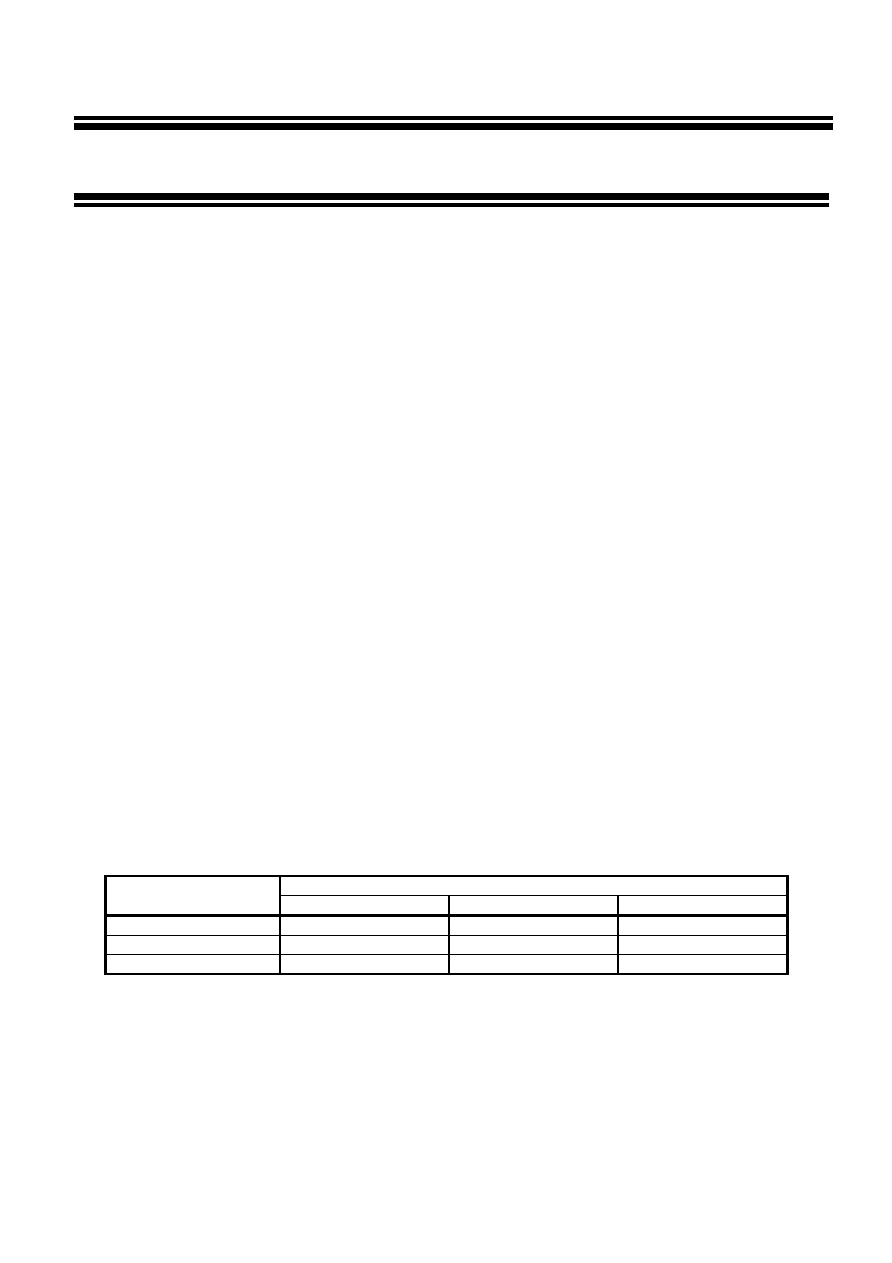
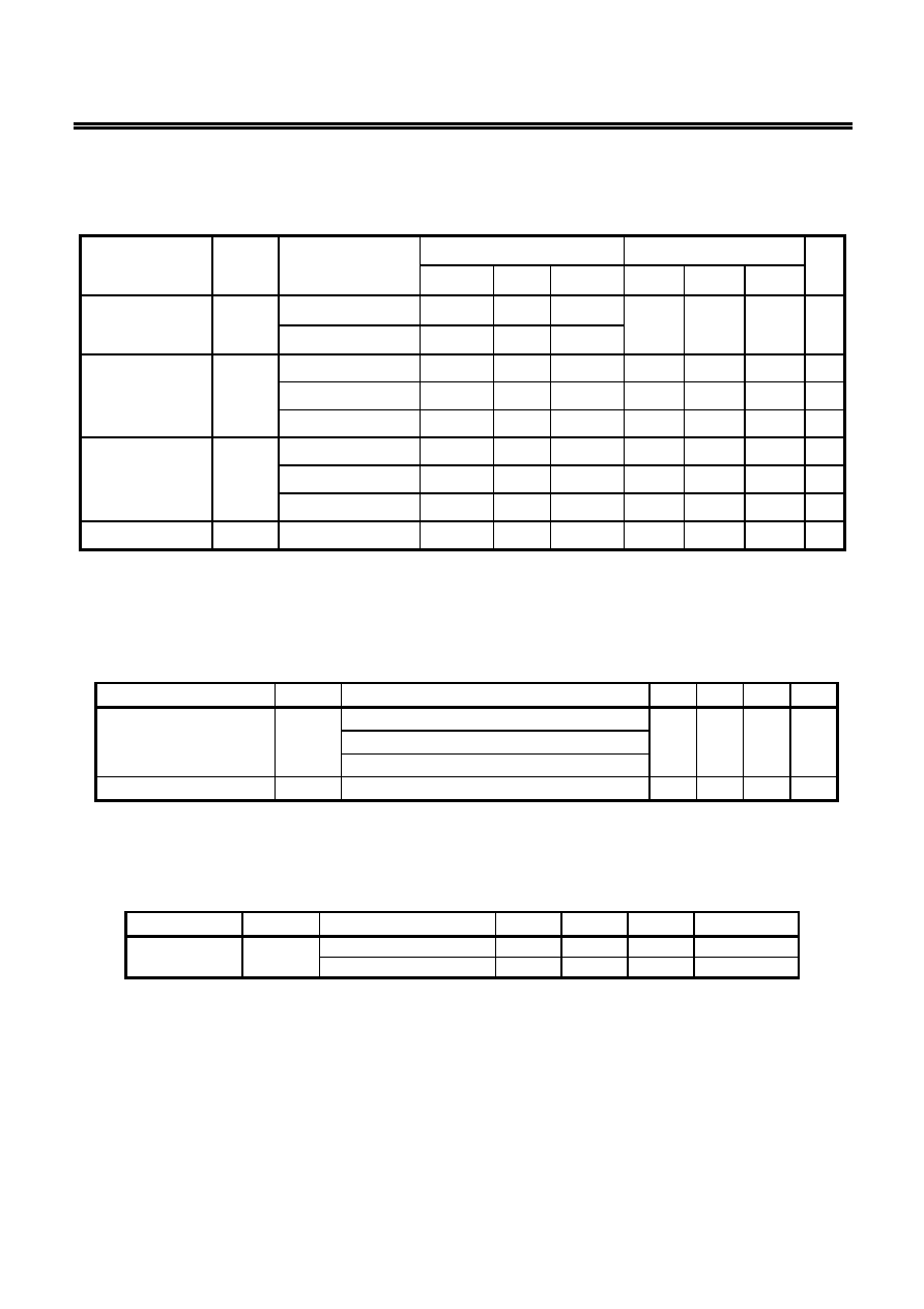
Pin Assignments
8-Pin DIP
Top view
Table 1
Pin
Number
Pin
Name
Function
1 A0
Address input (S-24CS04A/08A is no connect.
*1
)
2 A1
Address input (S-24CS08A is no connect.
*1
)
3 A2
Address
input
4 GND
Ground
5
SDA
Serial data input / output
6
SCL
Serial clock input
7 WP
Write protection input
Connected to V
CC
: Protection
valid
Connected to GND: Protection invalid
8 VCC
Power supply
*1. Connect to GND or V
CC
.
1
2
3
4
8
7
6
5
VCC
WP
SCL
SDA
A0
A1
GND
A2
Figure 1
S-24CS01ADP
S-24CS02ADP
S-24CS04ADP
S-24CS08ADP
Remark See Dimensions for details of the package drawings.
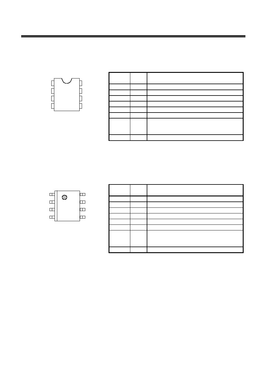
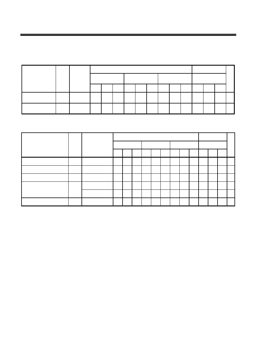
8-Pin SOP(JEDEC)
Top view
Table 2
Pin
Number
Pin
Name
Function
1 A0
Address input (S-24CS04A/08A is no connect.
*1
)
2 A1
Address input (S-24CS08A is no connect.
*1
)
3 A2
Address
input
4 GND
Ground
5
SDA
Serial data input / output
6
SCL
Serial clock input
7 WP
Write protection input
Connected to V
CC
: Protection
valid
Connected to GND: Protection invalid
8 VCC
Power supply
*1. Connect to GND or V
CC
.
1
2
3
4
8
7
6
5
VCC
WP
SCL
SDA
A0
A1
GND
A2
Figure 2
S-24CS01AFJ
S-24CS02AFJ
S-24CS04AFJ
S-24CS08AFJ
Remark See Dimensions for details of the package drawings.
2-WIRE CMOS SERIAL E
2
PROM
Rev.2.0
_10
S-24CS01A/02A/04A/08A
Seiko Instruments Inc.
3
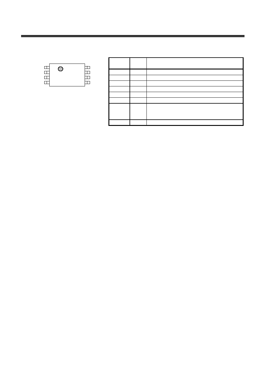
8-Pin TSSOP
Top view
Table 3
Pin
Number
Pin
Name
Function
1 A0
Address input (S-24CS04A/08A is no connect.
*1
)
2 A1
Address input (S-24CS08A is no connect.
*1
)
3 A2
Address
input
4 GND
Ground
5
SDA
Serial data input / output
6
SCL
Serial clock input
7 WP
Write protection input
Connected to V
CC
: Protection
valid
Connected to GND: Protection invalid
8 VCC
Power supply
*1. Connect to GND or V
CC
.
1
2
3
4
8
7
6
5
VCC
WP
SCL
SDA
A0
A1
GND
A2
Figure 3
S-24CS01AFT
S-24CS02AFT
S-24CS04AFT
S-24CS08AFT
Remark See Dimensions for details of the package drawings.
2-WIRE CMOS SERIAL E
2
PROM
S-24CS01A/02A/04A/08A
Rev.2.0
_10
Seiko Instruments Inc.
4
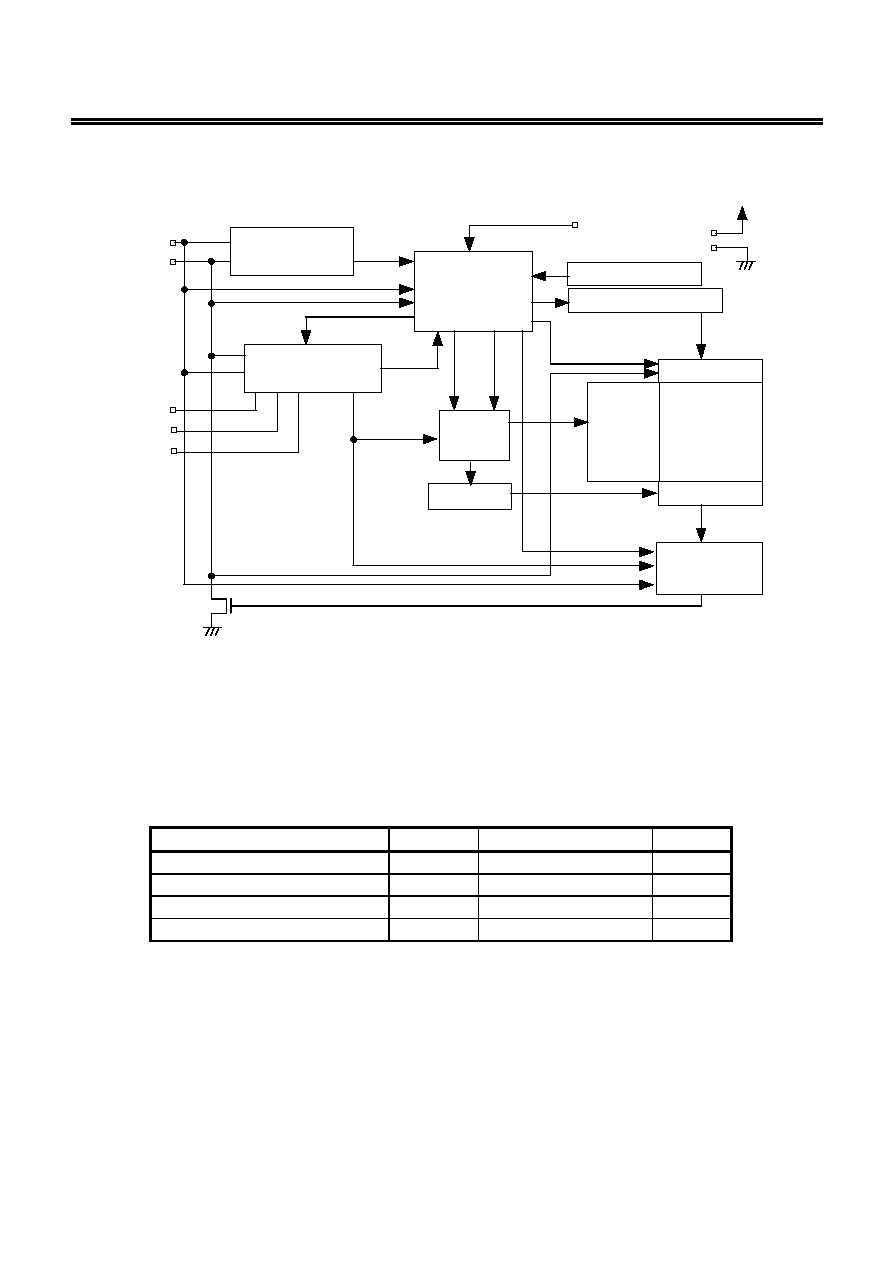
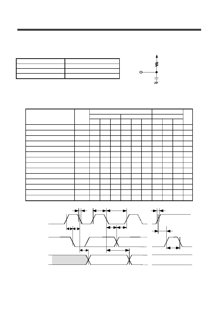
Block diagram
VCC
GND
Serial Clock
Controller
Device Address
Comparator
Address
Counter
Y Decoder
Data Output
ACK Output
Controller
Start / Stop
Detector
Data Register
E
2
PROM
X Decoder
Selector
High-Voltage Generator
SCL
SDA
A2
D
IN
D
OUT
R / W
LOAD
INC
COMP
LOAD
WP
A1
*1
A0
*2
Voltage Detector
*1. S-24CS08A is not available.
*2. S-24CS04A/08A are not available.
Figure 4
Absolute Maximum Ratings
Table 4
Parameter Symbol
Ratings
Unit
Power supply voltage
V
CC
-0.3 to +7.0 V
Input voltage
V
IN
-0.3 to V
CC
+0.3 V
Output voltage
V
OUT
-0.3 to V
CC
V
Storage temperature
T
stg
-65 to +150 ∞C
Caution The absolute maximum ratings are rated values exceeding which the
product could suffer physical damage. These values must therefore not be
exceeded under any conditions.
2-WIRE CMOS SERIAL E
2
PROM
Rev.2.0
_10
S-24CS01A/02A/04A/08A
Seiko Instruments Inc.
5
Recommended Operating Conditions
Table 5
Parameter
Symbol Conditions
-40 to +85∞C
-40 to +105∞C
Unit
Min.
Typ.
Max.
Min.
Typ.
Max.
Power supply voltage
V
CC
Read
Operation 1.8
5.5
Write
Operation
2.7
5.5
4.5
5.5 V
High level input voltage
V
IH
V
CC
=4.5 to 5.5 V
0.7
◊V
CC
V
CC
0.7
◊V
CC
V
CC
V
V
CC
=2.7 to 4.5 V
0.7
◊V
CC
V
CC
V
V
CC
=1.8 to 2.7 V
0.8
◊V
CC
V
CC
V
Low level input voltage
V
IL
V
CC
=4.5 to 5.5 V
0.0
0.3◊V
CC
0.0
0.3◊V
CC
V
V
CC
=2.7 to 4.5 V
0.0
0.3◊V
CC
V
V
CC
=1.8 to 2.7 V
0.0
0.2
◊V
CC
V
Operating temperature
T
opr
-40
+85
-40
+105
∞C
Pin Capacitance
Table 6
(Ta
=25∞C, f=1.0 MHz, V
CC
=5 V)
Parameter Symbol
Conditions
Min. Typ. Max. Unit
Input capacitance
C
IN
V
IN
=0 V (S-24CS01A/02A: SCL, A0, A1, A2, WP)
-- -- 10 pF
V
IN
=0 V (S-24CS04A: SCL, A1, A2, WP)
V
IN
=0 V (S-24CS08A: SCL, A2, WP)
Input/output capacitance
C
I / O
V
I / O
=0 V (SDA)
-- -- 10 pF
Endurance
Table 7
Parameter Symbol
Operation
temperature Min. Typ. Max.
Unit
Endurance N
W
-40 to +85∞C
10
6
--
--
cycles / word
-40 to +105∞C 3◊10
5
--
--
cycles / word
2-WIRE CMOS SERIAL E
2
PROM
S-24CS01A/02A/04A/08A
Rev.2.0
_10
Seiko Instruments Inc.
6
DC Electrical Characteristics
Table 8
Parameter Symbol
Conditions
-40 to +85∞C
-40 to +105∞C Unit
V
CC
=4.5 to 5.5 V
f = 400 kHz
V
CC
=2.7 to 4.5 V
f = 100 kHz
V
CC
=1.8 to 2.7 V
f = 100 kHz
V
CC
=4.5 to 5.5 V
f = 350 kHz
Min. Typ. Max. Min. Typ. Max. Min. Typ. Max. Min. Typ. Max.
Current consumption
(READ)
I
CC1
0.8
0.3
0.2
0.8
mA
Current consumption
(WRITE)
I
CC2
4.0
1.5
4.0
mA
Table 9
Parameter
Symbol
Conditions
-40 to +85∞C
-40 to +105∞C Unit
V
CC
=4.5 to 5.5 V V
CC
=2.7 to 4.5 V V
CC
=1.8 to 2.7 V V
CC
=4.5 to 5.5 V
Min. Typ. Max. Min. Typ. Max. Min. Typ. Max. Min. Typ. Max.
Standby current consumption
I
SB
V
IN
=V
CC
or GND
2.0 2.0 2.0 2.0 µA
Input leakage current
I
LI
V
IN
=GND to V
CC
0.1 1.0 0.1 1.0 0.1 1.0 0.1 1.0 µA
Output leakage current
I
LO
V
OUT
=GND to V
CC
0.1 1.0 0.1 1.0 0.1 1.0 0.1 1.0 µA
Low level output voltage
V
OL
I
OL
=3.2 mA
0.4 0.4 0.4 V
I
OL
=1.5 mA
0.3 0.3 0.5 0.3 V
Current address hold voltage
V
AH
1.5
5.5 1.5 4.5 1.5 2.7 1.5 5.5 V
2-WIRE CMOS SERIAL E
2
PROM
Rev.2.0
_10
S-24CS01A/02A/04A/08A
Seiko Instruments Inc.
7
AC Electrical Characteristics
Table 10 Measurement Conditions
Input pulse voltage
0.1
◊V
CC
to 0.9
◊V
CC
Input pulse rising / falling time
20 ns
Output judgment voltage
0.5
◊V
CC
Output load
100 pF
+ Pullup resistance 1.0 k
V
CC
R=1.0 k
SDA
C=100 pF
Figure 5 Output Load Circuit
Table 11
Parameter Symbol
-40 to +85∞C
-40 to +105∞C
Unit
V
CC
=4.5 to 5.5 V
V
CC
=1.8 to 4.5 V
V
CC
=4.5 to 5.5 V
Min. Typ. Max. Min. Typ. Max. Min. Typ. Max.
SCL clock frequency
f
SCL
0
400 0
100 0
350 kHz
SCL clock time "L"
t
LOW
1.0
4.7
1.1
µs
SCL clock time"H"
t
HIGH
0.9
4.0
1.0
µs
SDA output delay time
t
AA
0.1
0.9 0.1
3.5 0.1
1.0
µs
SDA output hold time
t
DH
50
100
50
ns
Start condition setup time
t
SU.STA
0.6
4.7
0.6
µs
Start condition hold time
t
HD.STA
0.6
4.0
0.6
µs
Data input setup time
t
SU.DAT
100
200
100
ns
Data input hold time
t
HD.DAT
0
0
0
ns
Stop condition setup time
t
SU.STO
0.6
4.7
0.6
µs
SCL SDA rising time
t
R
0.3
1.0
0.3
µs
SCL SDA falling time
t
F
0.3
0.3
0.3
µs
Bus release time
t
BUF
1.3
4.7
1.3
µs
Noise suppression time
t
I
50
100
50
ns
SCL
SDA IN
SDA OUT
t
BUF
t
R
t
SU.STO
t
SU.DAT
t
HD.DAT
t
DH
t
AA
t
HIGH
t
LOW
t
HD.STA
t
SU.STA
t
F
Figure 6 Bus Timing
2-WIRE CMOS SERIAL E
2
PROM
S-24CS01A/02A/04A/08A
Rev.2.0
_10
Seiko Instruments Inc.
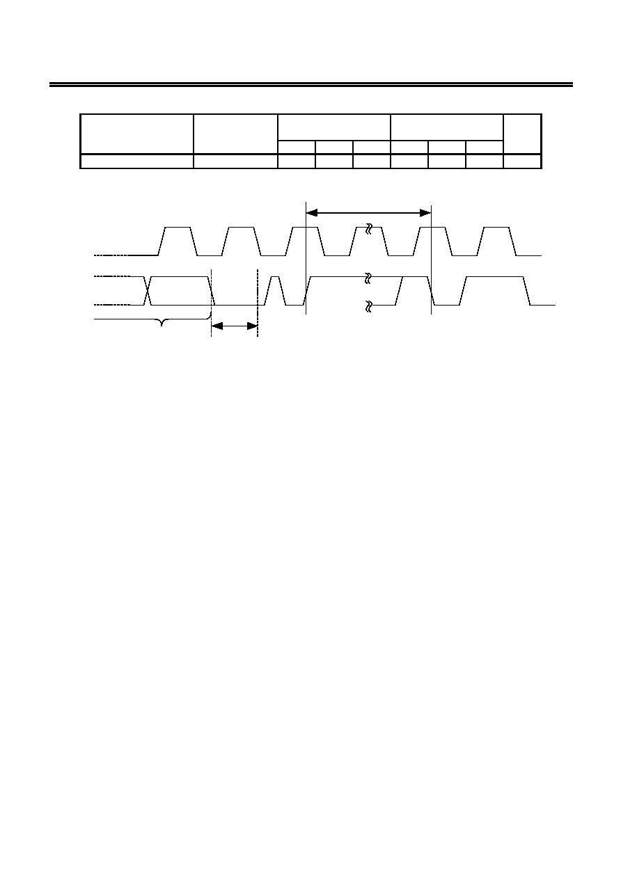
8
Table 12
Item Symbol
-40 to +85∞C
-40 to +105∞C
Unit
V
CC
=2.7 to 5.5 V
V
CC
=4.5 to 5.5 V
Min. Typ. Max. Min. Typ. Max.
Write time
t
WR
-- 4.0 10.0 -- 4.0 10.0 ms
SCL
SDA
D0
Write data
Acknowledge
Stop Condition
Start Condition
t
WR
Figure 7 Write Cycle Timing

2-WIRE CMOS SERIAL E
2
PROM
Rev.2.0
_10
S-24CS01A/02A/04A/08A
Seiko Instruments Inc.
9
Pin Functions
1. Address Input Pins (A0, A1 and A2)
The slave address is assigned by connecting pins A0, A1 and A2 to the GND or to the V
CC
respectively.
One of the eight different slave address can be assigned to the S-24CS01A/02A by the combination of pins
A0, A1 and A2.
The slave address is assigned by connecting pins A1 and A2 to the GND or to the V
CC
respectively. One of
the four different slave address can be assigned to the S-24CS04A by the combination of pins A1 and A2.
The slave address is assigned by connecting the A2 pin to the GND or to the V
CC
respectively. The two
different slave address can be assigned to the S-24CS08A by A2 pin.
The given slave address, which is compared with the slave address transmitted from the master device, is
used to select the one among the multiple devices connected to the bus. The address input pin should be
connected to the GND or to the V
CC
.
2. SDA (Serial Data Input / Output) Pin
The SDA pin is used for bi-directional transmission of serial data. It consists of a signal input pin and an
Nch open-drain output pin.
The SDA line is usually pulled up to the V
CC
, and OR-wired with other open-drain or open-collector output
devices.
3. SCL (Serial Clock Input) Pin
The SCL pin is used for serial clock input. Since signals are processed at the rising or falling edge of the
SCL clock input signal, attention should be paid to the rising time and falling time to conform to the
specifications.
4. WP Pin
The write protection is enabled by connecting the WP pin to the V
CC
. When there is no need for write
protection, connect the pin to the GND.
Remark Please refer to the Application Note "TIPS,TRICKS AND TRAPS WHEN USING THE S-24C/24CS
SERIES" for equivalent circuit of each pin.
2-WIRE CMOS SERIAL E
2
PROM
S-24CS01A/02A/04A/08A
Rev.2.0
_10
Seiko Instruments Inc.
10
Operation
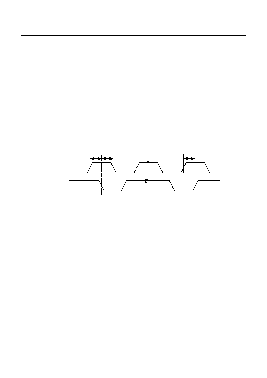
1. Start Condition
Start is identified by a high to low transition of the SDA line while the SCL line is stable at high.
Every operation begins from a start condition.
2. Stop Condition
Stop is identified by a low to high transition of the SDA line while the SCL line is stable at high.
When a device receives a stop condition during a read sequence, the read operation is interrupted, and the
device enters standby mode.
When a device receives a stop condition during a write sequence, the reception of the write data is halted,
and the E
2
PROM initiates a write cycle.
t
SU.STA
t
HD.STA
t
SU.STO
Start Condition
Stop Condition
SCL
SDA
Figure 8 Start / Stop Conditions
2-WIRE CMOS SERIAL E
2
PROM
Rev.2.0
_10
S-24CS01A/02A/04A/08A
Seiko Instruments Inc.
11
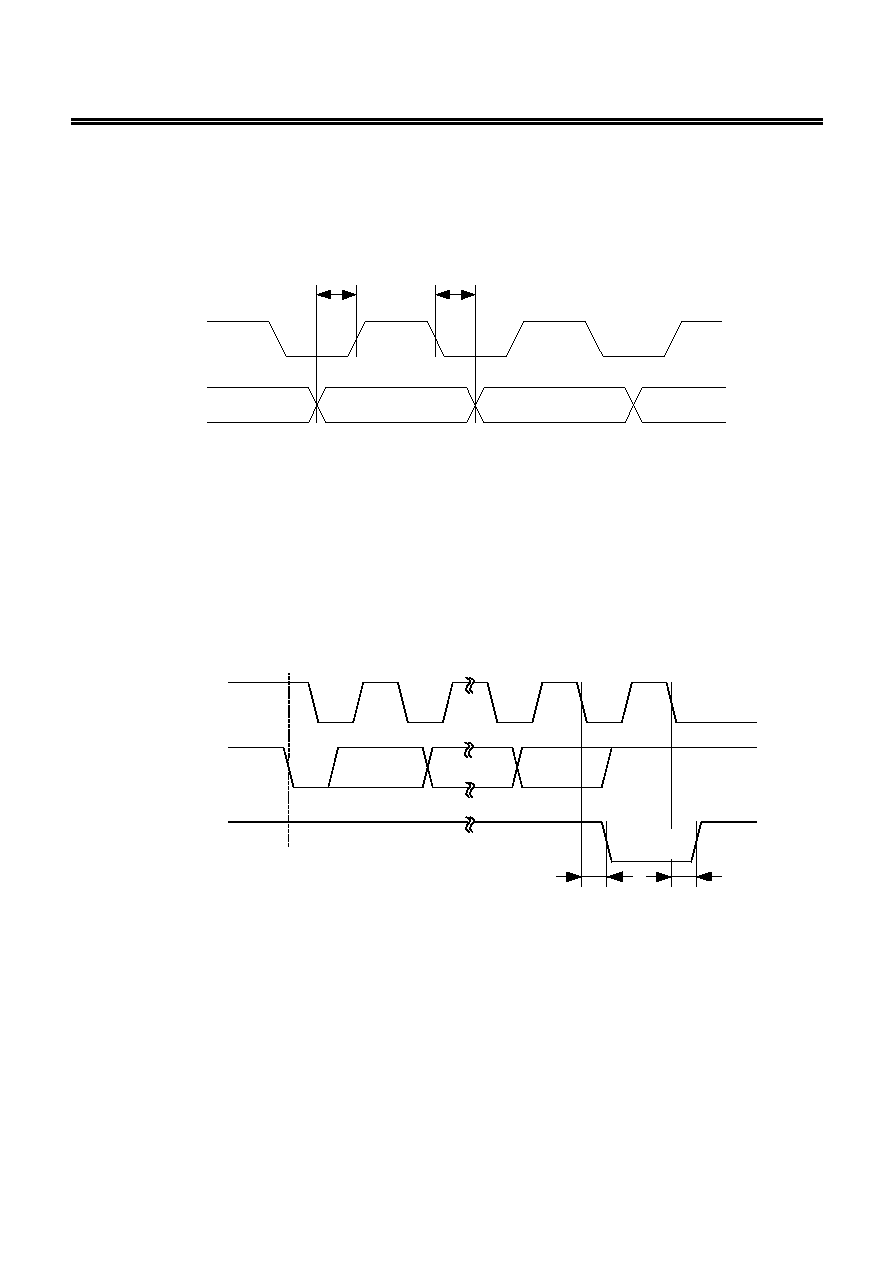
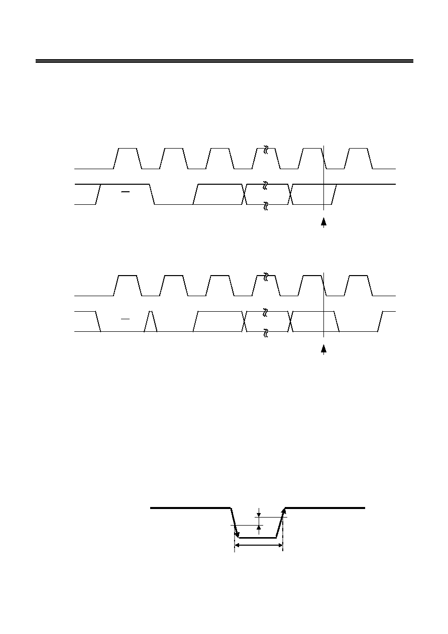
3. Data Transmission
Changing the SDA line while the SCL line is low, data is transmitted.
Changing the SDA line while the SCL line is high, a start or stop condition is recognized.
t
SU.DAT
t
HD.DAT
SCL
SDA
Figure 9 Data Transmission Timing
4. Acknowledge
The unit of data transmission is 8 bits. During the 9th clock cycle period the receiver on the bus pulls down
the SDA line to acknowledge the receipt of the 8-bit data.
When a internal write cycle is in progress, the device does not generate an acknowledge.
1
8
9
Acknowledge
Output
t
AA
t
DH
Start Condition
SCL
(E
2
PROM Input)
SDA
(Master Output)
SDA
(E
2
PROM Output)
Figure 10 Acknowledge Output Timing
2-WIRE CMOS SERIAL E
2
PROM
S-24CS01A/02A/04A/08A
Rev.2.0
_10
Seiko Instruments Inc.
12
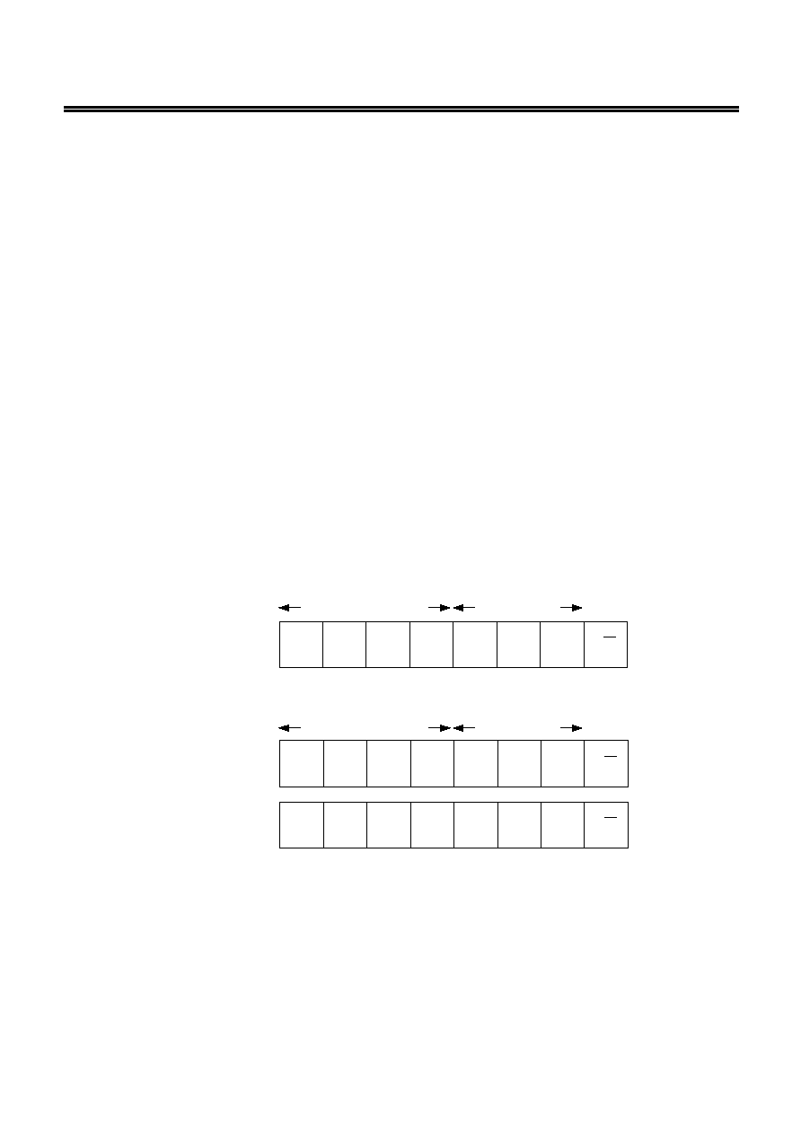
5. Device Addressing
To start communication, the master device on the system generates a start condition to the bus line. Next,
the master device sends 7-bit device address and a 1-bit read / write instruction code on to the SDA bus.
The 4 most significant bits of the device address are called the "Device Code", and are fixed to "1010".
In S-24CS01A/02A, successive 3 bits are called the "Slave Address". These 3 bits are used to identify a
device on the system bus and are compared with the predetermined value which is defined by the address
input pins (A0, A1 and A2). When the comparison result matches, the slave device responds with an
acknowledge during the 9th clock cycle.
In S-24CS04A, successive 2 bits are called the "Slave Address." These 2 bits are used to identify a device
on the system bus and are compared with the predetermined value which is defined by the address input
pins (A1 and A2). When the comparison result matches, the slave device responds with an acknowledge
during the 9th clock cycle.
The successive 1 bit (P0) is used to define a page address and choose the two 256-byte memory blocks
(Address 000h to 0FFh and 100h to 1FFh).
In S-24CS08A, successive 1 bit is called the "Slave Addrdess". This 1 bit is used to identify a device on the
system bus and is compared with the predetermined value which is defined by the address input pin (A2).
When the comparison result matches, the slave device responds with an acknowledge during the 9th
clocks cycle.
The successive 2 bits (P1 and P0) are used to define a page address and choose the four 256-byte
memory blocks (Address 000h to 0FFh, 100h to 1FFh, 200h to 2FFh and 300h to 3FFh).
Slave Address
1
0
1
0
A2
A1
A0
R/W
Device Code
LSB
MSB
S-24CS01A/02A
Slave / Page
Address
Device Code
S-24CS04A
1
0
1
0
A2
A1
P0
R/W
1
0
1
0
A2
P1
P0
R/W
LSB
MSB
S-24CS08A
Figure 11 Device Address
2-WIRE CMOS SERIAL E
2
PROM
Rev.2.0
_10
S-24CS01A/02A/04A/08A
Seiko Instruments Inc.
13
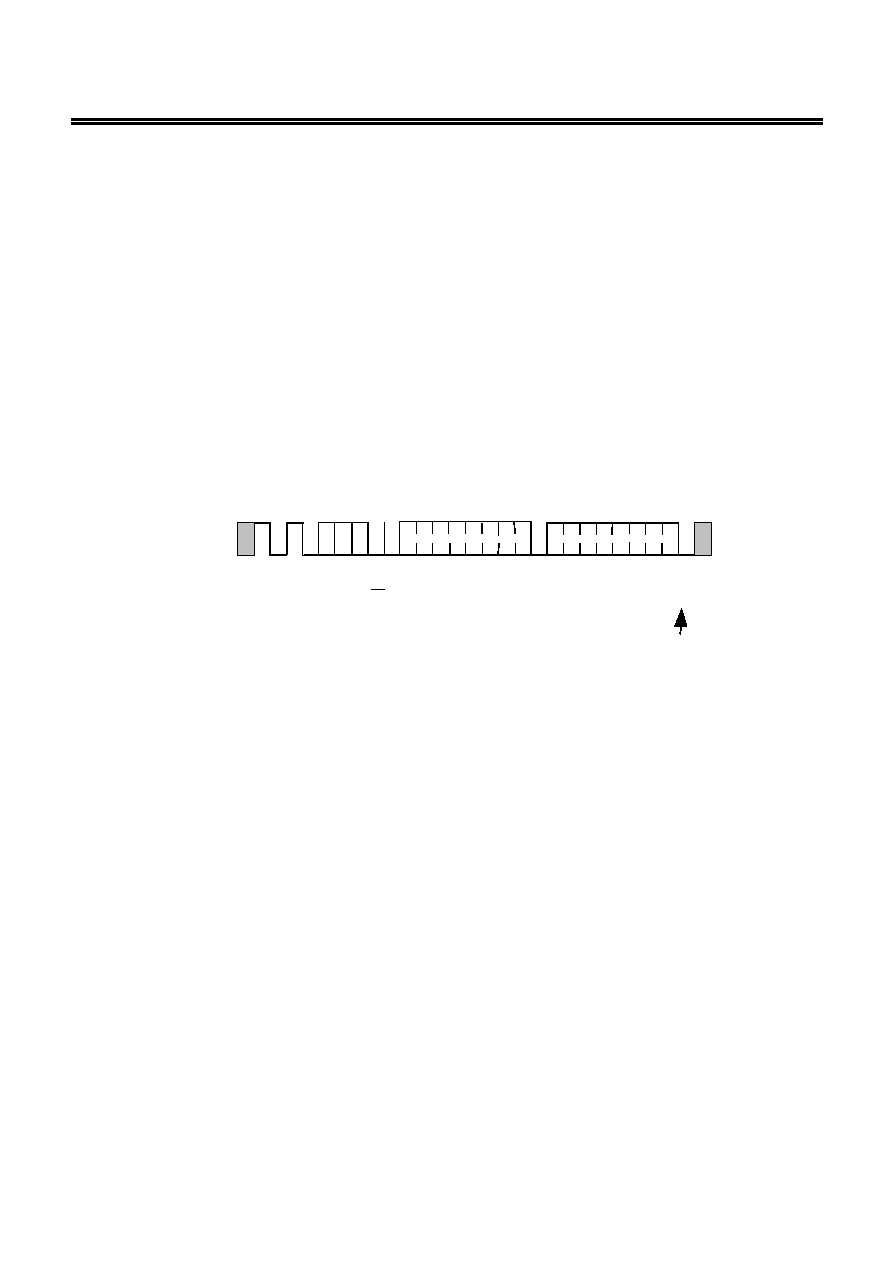
6. Write
6.1 Byte Write
When the master sends a 7-bit device address and a 1-bit read / write instruction code set to "0", following
a start condition, the E
2
PROM acknowledges it. The E
2
PROM then receives an 8-bit word address and
responds with an acknowledge. After the E
2
PROM receives 8-bit write data and responds with an
acknowledge, it receives a stop condition and that initiates the write cycle at the addressed memory.
During the write cycle all operations are forbidden and no acknowledge is generated.
A2 A1 A0
S
T
A
R
T
1
0 1 0
W
R
I
T
E
DEVICE
ADDRESS
R
/
W
M
S
B
SDA LINE
ADR INC
(ADDRESS INCREMENT)
A
C
K
L
S
B
0
WORD ADDRESS
S
T
O
P
DATA
W7 W6 W5 W4 W3 W2 W1 W0
D7 D6 D5 D4 D3 D2 D1 D0
A
C
K
A
C
K
Remark1. A1 is P1 in the S-24CS08A.
2. A0 is P0 in the S-24CS04A/08A.
3. W7 is optional in the S-24CS01A.
Figure 12 Byte Write
2-WIRE CMOS SERIAL E
2
PROM
S-24CS01A/02A/04A/08A
Rev.2.0
_10
Seiko Instruments Inc.
14
6.2 Page Write
The page write mode allows up to 8 bytes to be written in a single wire operation in the S-24CS01A/02A
and 16 bytes to be written in a single write operation in the S-24CS04A/08A.
Basic data transmission procedure is the same as that in the "Byte Write". But instead of generating a stop
condition, the master transmitts 8-bit write data up to 8 bytes before the page write.
When the E
2
PROM receives a 7-bit device address and a 1-bit read / write instruction code set to "0",
following a start condition, it generates an acknowledge. Then the E
2
PROM receives an 8-bit word
address, and responds with an acknowledge. After the E
2
PROM receives 8-bit write data and responds
with an acknowledge, it receives 8-bit write data corresponding to the next word address, and generates
an acknowledge. The E
2
PROM repeats reception of 8-bit write data and generation of acknowledge in
succession. The E
2
PROM can receive as many write data as the maximum page size.
Receiving a stop condition initiates a write cycle of the area starting from the designated memory address
and having the page size equal to the received write data.
S
T
A
R
T
1
0 1 0
W
R
I
T
E
S
T
O
P
DEVICE
ADDRESS
WORD ADDRESS (n)
R
/
W
M
S
B
SDA
LINE
A2 A1 A0
A
C
K
L
S
B
A
C
K
A
C
K
0
D7 D6 D5 D4 D3 D2 D1 D0
D7
D0
D7
D0
A
C
K
ADR INC
ADR INC
A
C
K
DATA (n) DATA
(n+1)
DATA (n+x)
W7 W6 W5 W4 W3 W2 W1 W0
ADR INC
Remark1. A1 is P1 in the S-24CS08A.
2. A0 is P0 in the S-24CS04A/08A.
3. W7 is optional in the S-24CS01A.
Figure 13 Page Write
In S-24CS01A/02A, the lower 3 bits of the word address are automatically incremented every time when
the E
2
PROM receives 8-bit write data. If the size of the write data exceeds 8 bytes, the upper 5 bits of the
word address remain unchanged, and the lower 3 bits are rolled over and previously received data will be
overwritten.
In S-24CS04A, the lower 4 bits of the word address are automatically incremented every time when the
E
2
PROM receives 8-bit write data. If the size of the write data exceeds 16 bytes, the upper 4 bits of the
word address and page address (P0) remain unchanged, and the lower 4 bits are rolled over and
previously received data will be overwritten.
In S-24CS08A, the lower 4 bits of the word address are automatically incremented every time when the
E
2
PROM receives 8-bit write data. If the size of the write data exceeds 16 bytes, the upper 4 bits of the
word address and page address (P1 and P0) remain unchanged, and the lower 4 bits are rolled over and
previously received data will be overwritten.

2-WIRE CMOS SERIAL E
2
PROM
Rev.2.0
_10
S-24CS01A/02A/04A/08A
Seiko Instruments Inc.
15
6.3 Acknowledge Polling
Acknowledge polling is used to know the completion of the write cycle in the E
2
PROM.
After the E
2
PROM receives a stop condition and once starts the write cycle, all operations are forbidden
and no response is made to the signal transmitted by the master device.
Accordingly the master device can recognize the completion of the write cycle in the E
2
PROM by detecting
a response from the slave device after transmitting the start condition, the device address and the
read/write instruction code to the E
2
PROM, namely to the slave devices.
That is, if the E
2
PROM does not generate an acknowledge, the write cycle is in progress and if the
E
2
PROM generates an acknowledge, the write cycle has been completed.
It is recommended to use the read instruction "1" as the read/write instruction code transmitted by the
master device.
6.4 Write Protection
Write protection is available in the S-24CS01A/02A/04A/08A. When the WP pin is connected to the V
CC
,
write operation to memory area is forbidden at all.
When the WP pin is connected to the GND, the write protection is invalid, and write operation in all memory
area is available. There is no need for using write protection, the WP pin should be connected to the GND.
The write protection is valid in the operating voltage range.
2-WIRE CMOS SERIAL E
2
PROM
S-24CS01A/02A/04A/08A
Rev.2.0
_10
Seiko Instruments Inc.
16
7. Read
7.1 Current Address Read
Either in writing or in reading the E
2
PROM holds the last accessed memory address, internally
incremented by one. The memory address is maintained as long as the power voltage is higher than the
current address hold voltage V
AH
.
The master device can read the data at the memory address of the current address pointer without
assigning the word address as a result, when it recognizes the position of the address pointer in the
E
2
PROM. This is called "Current Address Read".
In the following the address counter in the E
2
PROM is assumed to be "n".
When the E
2
PROM receives a 7-bit device address and a 1-bit read / write instruction code set to "1"
following a start condition, it responds with an acknowledge. However, the page address (P0) in S-
24CS04A and the page address (P1 and P0) in S-24CS08A become invalid and the memory address of
the current address pointer becoms valid.
Next an 8-bit data at the address "n" is sent from the E
2
PROM synchronous to the SCL clock. The address
counter is incremented at the falling edge of the SCL clock for the 8th bit data, and the content of the
address counter becomes n
+1.
The master device has to not acknowledge the 8-bit data and terminates the reading with a stop condition.
S
T
A
R
T
1 0 1 0
R
E
A
D
S
T
O
P
DEVICE
ADDRESS
R
/
W
M
S
B
SDA LINE
A2 A1 A0
D7 D6 D5 D4 D3 D2 D1 D0
A
C
K
L
S
B
ADR INC
1
DATA
NO ACK from
Master Device
Remark1. A1 is P1 in S-24CS08A.
2. A0 is P0 in S-24CS04A/08A.
Figure 14 Current Address Read
Attention should be paid to the following point on the recognition of the address pointer in the E
2
PROM.
In the read operation the memory address counter in the E
2
PROM is automatically incremented at every
falling edge of the SCL clock for the 8th bit of the output data. In the write operation, on the other hand, the
upper bits of the memory address (the upper bits of the word address and page address)
*1
are left
unchanged and are not incremented at the falling edge of the SCL clock for the 8th bit of the received
data.
*1. S-24CS01A/02A is the upper 5 bits of the word address.
S-24CS04A is the upper 4 bits of the word address and the page address P0.
S-24CS08A is the upper 4 bits of the word address and the page address P1 and P0.
2-WIRE CMOS SERIAL E
2
PROM
Rev.2.0
_10
S-24CS01A/02A/04A/08A
Seiko Instruments Inc.
17
7.2 Random Read
Random read is used to read the data at an arbitrary memory address.
A dummy write is performed to load the memory address into the address counter.
When the E
2
PROM receives a 7-bit device address and a 1-bit read / write instruction code set to "0"
following a start condition, it responds with an acknowledge. The E
2
PROM then receives an 8-bit word
address and responds with an acknowledge. The memory address is loaded to the address counter in the
E
2
PROM by these operations. Reception of write data does not follow in a dummy write whereas reception
of write data follows in a byte write and in a page write.
Since the memory address is loaded into the memory address counter by dummy write, the master device
can read the data starting from the arbitrary memory address by transmitting a new start condition and
performing the same operation in the current address read.
That is, when the E
2
PROM receives a 7-bit device address and a 1-bit read / write instruction code set to
"1", following a start condition signal, it responds with an acknowledge. Next, 8-bit data is transmitted from
the E
2
PROM in synchronous to the SCL clock. The master device has to not acknowledge and terminates
the reading with a stop condition.
SDA
LINE
S
T
A
R
T
W
R
I
T
E
DEVICE
ADDRESS
WORD
ADDRESS (n)
M
S
B
DUMMY WRITE
S
T
A
R
T
R
E
A
D
DEVICE
ADDRESS
M
S
B
A
C
K
L
S
B
NO ACK from
Master Device
S
T
O
P
ADR INC
DATA
A
C
K
A
C
K
L
S
B
R
/
W
R
/
W
Remark1. A1 is P1 in the S-24CS08A.
2. A0 is P0 in the S-24CS04A/08A.
3. W7 is optional in the S-24CS01A.
1 0 1 0 A2 A1 A0 0
W7 W6 W5 W4 W3 W2 W1 W0
1 0 1 0 A2 A1 A0 1
D7 D6 D5 D4 D3 D2 D1 D0
Figure 15 Random Read
2-WIRE CMOS SERIAL E
2
PROM
S-24CS01A/02A/04A/08A
Rev.2.0
_10
Seiko Instruments Inc.
18
7.3 Sequential Read
When the E
2
PROM receives a 7-bit device address and a 1-bit read / write instruction code set to "1"
following a start condition both in current and random read operations, it responds with an acknowledge.
An 8-bit data is then sent from the E
2
PROM synchronous to the SCL clock and the address counter is
automatically incremented at the falling edge of the SCL clock for the 8th bit data.
When the master device responds with an acknowledge, the data at the next memory address is
transmitted. Response with an acknowledge by the master device has the memory address counter in the
E
2
PROM incremented and makes it possible to read data in succession. This is called "Sequential Read".
The master device has not acknowledge and terminates the reading with a stop condition.
Data can be read in succession in the sequential read mode. When the memory address counter reaches
the last word address, it rolls over to the first memory address.
R
E
A
D
S
T
O
P
DEVICE
ADDRESS
R
/
W
ADR INC
A
C
K
A
C
K
A
C
K
1
ADR INC
A
C
K
ADR INC
SDA
LINE
DATA(n)
D7
D0
D7
D0
D7
D0
D7
D0
DATA (n+1)
DATA (n+2)
DATA (n+x)
NO ACK from
Master Device
ADR INC
Figure 16 Sequential Read
2-WIRE CMOS SERIAL E
2
PROM
Rev.2.0
_10
S-24CS01A/02A/04A/08A
Seiko Instruments Inc.
19
8. Address Increment Timing
The timing for the automatic address increment is the falling edge of the SCL clock for the 8th bit of the
read data in read operation and the the falling edge of the SCL clock for the 8th bit of the received data in
write operation.
SCL
SDA
R / W=1
Address Increment
8
9
1
8
9
D7 Output
D0 Output
ACK Output
Figure 17 Address Increment Timing in Reading
SCL
SDA
R / W=0
8
9
1
8
9
D7 Input
D0 Input
ACK Output
ACK Output
Address Increment
Figure 18 Address Increment Timing in Writing
Write inhibition function at low power voltage
The S-24CS01A/02A/04A/08A have a detection circuit for low power voltage. The detection circuit cancels a
write instruction when the power voltage is low or the power switch is on. The detection voltage is 1.75 V
typically and the release voltage is 2.05 V typically, the hysteresis of approximate 0.3 V thus exists. (See
Figure 19.)
When a low power voltage is detected, a write instruction is canceled at the reception of a stop condition.
When the power voltage lowers during a data transmission or a write operation, the date at the address of
the operation is not assured.
Power supply voltage
Write Instruction
cancel
Release voltage (+V
DET
)
2.05 V typ.
Detection voltage (-V
DET
)
1.75 V typ.
Hysteresis width
0.3 V approximately
Figure 19 Operation at low power voltage

2-WIRE CMOS SERIAL E
2
PROM
S-24CS01A/02A/04A/08A
Rev.2.0
_10
Seiko Instruments Inc.
20
Precautions
Generally, an E
2
PROM may cause a malfunction by the operation in low voltage range induced by power
ON/OFF. The S-24CS01A/02A/04A/08A initialize themselves by the power on clear circuit at power on.
Attention should be paid to the followings so as to operate the power on clear circuit correctly, otherwise
malfunction may occur.
1. All input and output pins should be connected to the V
CC
or the GND level so as not to be floating.
2. Raise the power voltage up to the operation voltage from 0 V without staying at middle range.
3. Raising speed of the power voltage should be faster than 40 ms/V.
4. Power off interval before power on should be longer than 100 ms.
Do not apply an electrostatic discharge to this IC that exceeds the performance ratings of the built-in
electrostatic protection circuit.
SII claims no responsibility for any and all disputes arising out of or in connection with any infringement of
the products including this IC upon patents owned by a third party.
I
2
C Bus License
Purchase of I
2
C components of Seiko Instruments Inc., conveys a license under the Philips I
2
C Patent.
Rights to use these components in an I
2
C system, is granted provided that the system conforms to the I
2
C
Standard Specification as defined by Philips.
Please note that a product or a system incorporating this IC may infringe upon the Philips I
2
C Patent Rights
depending upon its configuration. In the event of such infringement Seiko Instruments Inc., shall not bear
any responsibility for any matters with regard to and arising from such patent infringement.
2-WIRE CMOS SERIAL E
2
PROM
Rev.2.0
_10
S-24CS01A/02A/04A/08A
Seiko Instruments Inc.
21
Typical Characteristics
1. DC Characteristics
1.1 Current consumption (READ) I
CC1
1.2 Current consumption (READ) I
CC1
Ambient temperature Ta
Ambient temperature Ta
V
CC
=5.5 V
f
SCL
=100 kHz
DATA=0101
-40 0
85
300
100
200
0
I
CC1
(
µA)
Ta (
∞C)
Ta (
∞C)
V
CC
=3.3 V
f
SCL
=100 kHz
DATA=0101
-40 0
85
300
100
200
0
I
CC1
(
µA)
1.3 Current consumption (READ) I
CC1
1.4 Current consumption (READ) I
CC1
Ambient temperature Ta
Power supply voltage V
CC
VCC= 1.8 V
f
SCL
=100 kHz
DATA=0101
300
100
200
0
I
CC1
(
µA)
Ta (
∞C)
-40 0
85
Ta=25
∞C
2 3 4 5 6 7
V
CC
(V)
300
100
200
0
I
CC1
(
µA)
f
CSL
=100 kHz
DATA=0101
1.5 Current consumption (READ) I
CC1
1.6 Current consumption (READ) I
CC1
Power supply voltage V
CC
Clock frequency f
SCL
Ta=25
∞C
2 3 4 5 6 7
V
CC
(V)
300
100
200
0
I
CC1
(
µA)
f
SCL
=400 kHz
DATA=0101
V
CC
=5.0 V
Ta=25
∞C
100 k
f
SCL
(Hz)
400 k 1 M
300
200
100
I
CC1
(
µA)
2-WIRE CMOS SERIAL E
2
PROM
S-24CS01A/02A/04A/08A
Rev.2.0
_10
Seiko Instruments Inc.
22
1.7 Current consumption (PROGRAM) I
CC2
1.8 Current consumption (PROGRAM) I
CC2
Ambient temperature Ta
Ambient temperature Ta
V
CC
=5.5 V
Ta (
∞C)
-40 0
85
1.0
0.5
0
I
CC2
(mA)
V
CC
=3.3 V
Ta (
∞C)
-40 0
85
1.0
0.5
0
I
CC2
(mA)
1.9 Current consumption (PROGRAM) I
CC2
1.10 Current consumption (PROGRAM) I
CC2
Ambient temperature Ta
Power supply voltage V
CC
V
CC
=2.5 V
1.0
0.5
0
I
CC2
(mA)
Ta (
∞C)
-40 0
85
Ta=25
∞C
V
CC
(V)
1.0
0.5
0
I
CC2
(mA)
2
1
3 4 5 6
1.11 Standby current consumption I
SB
1.12 Input leakage current I
LI
Ambient temperature Ta
Ambient temperature Ta
2.0
1.0
V
CC
=5.5 V
0
I
SB
(
µA)
Ta (
∞C)
-40 0
85
1.0
0.5
V
CC
=5.5 V
A0, A1, A2
0
I
LI
(
µA)
Ta (
∞C)
-40 0
85
SDA, SCL, WP=0 V
2-WIRE CMOS SERIAL E
2
PROM
Rev.2.0
_10
S-24CS01A/02A/04A/08A
Seiko Instruments Inc.
23
1.13 Input leakage current I
LI
1.14 Output leakage current I
LO
Ambient temperature Ta
Ambient temperature Ta
1.0
0.5
V
CC
=5.5 V
0
I
LI
(
µA)
Ta (
∞C)
-40 0
85
A0, A1, A2
SDA, SCL, P=5.5 V
1.0
0.5
V
CC
=5.5 V
SDA=0 V
0
I
LO
(
µA)
Ta (
∞C)
-40
0
85
1.15 Output leakage current I
LO
1.16 Low level output voltage V
OL
Ambient temperature Ta
Low level output current I
OL
1.0
0.5
V
CC
=5.5 V
SDA=5.5 V
0
I
LO
(
µA)
Ta (
∞C)
-40 0
85
0.6
0.4
V
OL
(V)
0.2
0
2
1 3
4
5
6
Ta=-40
∞C
I
OL
(mA)
V
CC
=1.8 V
V
CC
=5.0 V
1.17 Low level output voltage V
OL
1.18 Low level output voltage V
OL
Low level output current I
OL
Low level output current I
OL
0.6
0.4
V
OL
(V)
0.2
0
2
1 3
4
5
6
Ta=25
∞C
I
OL
(mA)
V
CC
=1.8 V
V
CC
=5.0 V
0.6
0.4
V
OL
(V)
0.2
0
2
1 3
4
5
6
Ta=85
∞C
I
OL
(mA)
V
CC
=1.8 V
V
CC
=5.0 V
2-WIRE CMOS SERIAL E
2
PROM
S-24CS01A/02A/04A/08A
Rev.2.0
_10
Seiko Instruments Inc.
24
1.19 High input inversion voltage V
IH
1.20 High input inversion voltage V
IH
Power supply voltage V
CC
Ambient temperature Ta
Ta=25∞C
A0, A1, A2,
1.0
0
2.0
3.0
V
IH
(V)
V
CC
(V)
7
6
2 3 4 5
1
SDA, SCL, WP
V
CC
=5.0 V
A0, A1, A2
1.0
0
2.0
3.0
V
IH
(V)
Ta (
∞C)
-40 0
85
SDA, SCL, WP
1.21 Low input inversion voltage V
IL
1.22 Low input inversion voltage V
IL
Power supply voltage V
CC
Ambient temperature Ta
Ta=25∞C
A0, A1, A2,
1.0
0
2.0
3.0
V
IL
(V)
V
CC
(V)
7
6
2 3 4 5
1
SDA, SCL, WP
V
CC
=5.0 V
A0, A1, A2,
1.0
0
2.0
3.0
V
IL
(V)
Ta (
∞C)
-40 0
85
SDA, SCL, WP
1.23 Low power supply detection voltage
-V
DET
1.24 Low power supply release voltage
+V
DET
Ambient temperature Ta
Ambient temperature Ta
1.0
0
2.0
-V
DET
(V)
Ta (
∞C)
-40 0
85
1.0
0
2.0
+V
DET
(V)
Ta (
∞C)
-40 0
85
2-WIRE CMOS SERIAL E
2
PROM
Rev.2.0
_10
S-24CS01A/02A/04A/08A
Seiko Instruments Inc.
25
2. AC Characteristics
2.1 Maximum operating frequency f
max.
2.2 Write time t
WR
Power supply voltage V
CC
Power supply voltage V
CC
10 k
2 3 4 5
Ta=25
∞C
V
CC
(V)
f
max
(Hz)
1
100 k
1 M
V
CC
(V)
8
4
Ta=25
∞C
t
WR
(ms)
2
6
0
6
2 3 4 5
1
2.3 Write time t
WR
Ambient temperature Ta
2.4 Write time t
WR
Ambient temperature Ta
V
CC
=2.5 V
t
WR
(ms)
9
6
3
0
Ta (
∞C)
-40 0
85
V
CC
=2.5 V
t
WR
(ms)
9
6
3
0
Ta (
∞C)
-40 0
85
2.5 SDA output delay time t
AA
2.6 SDA output delay time t
AA
Ambient temperature Ta
Ambient temperature Ta
Ta (
∞C)
-40 0
85
V
CC
=4.5 V
1.0
0.5
t
AA
(
µs)
0
Ta (
∞C)
-40 0
85
V
CC
=2.7 V
1.0
0.5
t
AA
(
µs)
0
2-WIRE CMOS SERIAL E
2
PROM
S-24CS01A/02A/04A/08A
Rev.2.0
_10
Seiko Instruments Inc.
26
2.7 SDA output delay time t
AA
Ambient temperature Ta
Ta (
∞C)
-40 0
85
V
CC
=1.8 V
1.0
0.5
t
AA
(
µs)
0
Ordering Information
Operation temperature
none:
-40 to +85∞C
H:
-40 to +105∞C (Only 8-Pin SOP(JEDEC))
IC direction in tape specification (Except 8-Pin DIP)
Package name (abbreviation) and IC packing specifications
DP: 8-Pin DIP, Tube
FJ: 8-Pin SOP(JEDEC), Tape
FT: 8-Pin TSSOP, Tape
Product name
S-24CS01A : 1k bit
S-24CS02A : 2k bit
S-24CS04A : 4k bit
S-24CS08A : 8k bit
S-24CS0xA xx
- TB x
No.
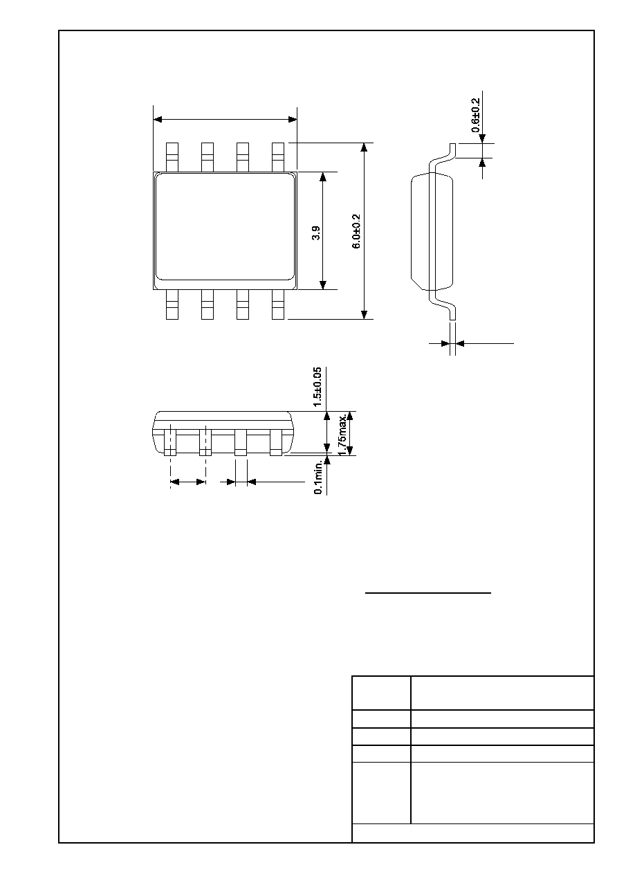
TITLE
SCALE
UNIT
mm
Seiko Instruments Inc.
DIP8-F-PKG Dimensions
No. DP008-F-P-SD-1.1
DP008-F-P-SD-1.1
0.48±0.1
2.54
0.89
1.3
0∞ to 15∞
0.25
+0.11
-0.05
7.62
9.6(10.6max.)
1
4
5
8
No. FJ008-A-P-SD-2.1
0.4±0.05
1.27
0.20±0.05
5.02±0.2
1
4
8
5
No.
TITLE
SCALE
UNIT
mm
SOP8J-A-PKG Dimensions
Seiko Instruments Inc.
FJ008-A-P-SD-2.1
No.
TITLE
SCALE
UNIT
mm
5
8
1
4
¯2.0±0.05
¯1.55±0.05
0.3±0.05
2.1±0.1
8.0±0.1
5∞max.
6.7±0.1
2.0±0.05
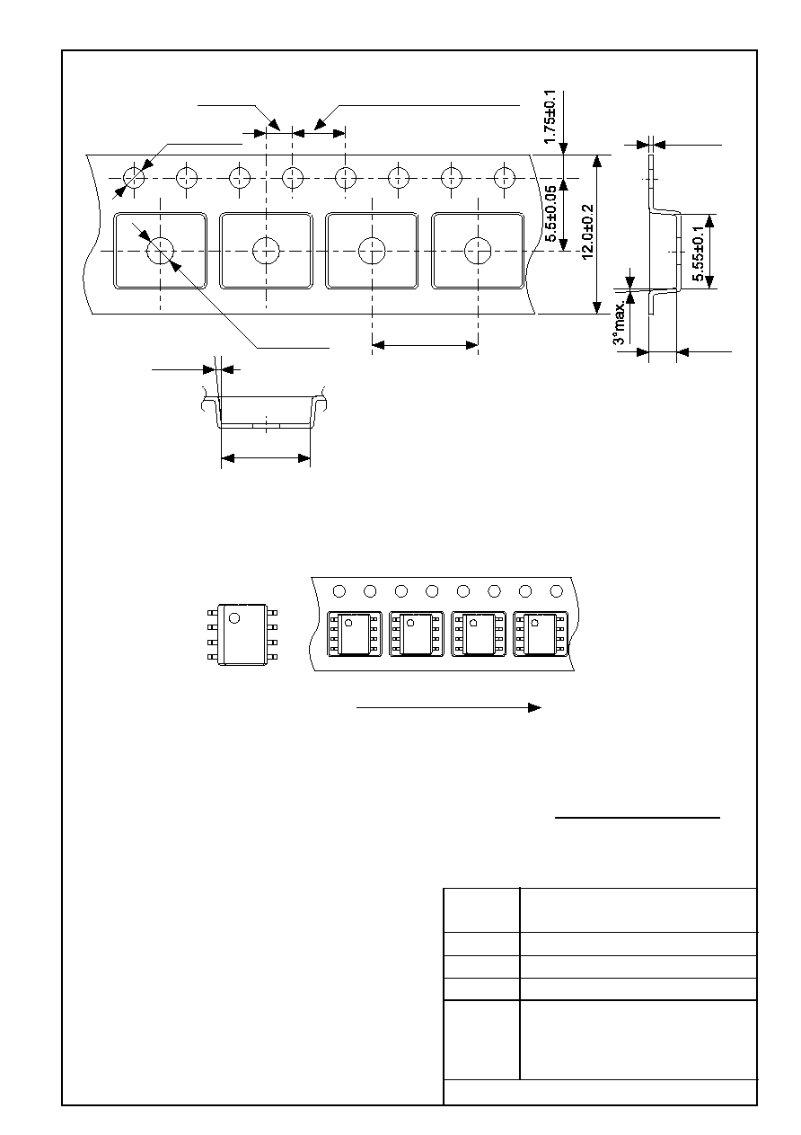
Seiko Instruments Inc.
Feed direction
4.0±0.1(10 pitches:40.0±0.2)
SOP8J-D-Carrier Tape
No. FJ008-D-C-SD-1.1
FJ008-D-C-SD-1.1
No.
TITLE
SCALE
UNIT
mm
QTY.
2,000
2±0.5
13.5±0.5
60∞
2±0.5
¯13±0.2
¯21±0.8
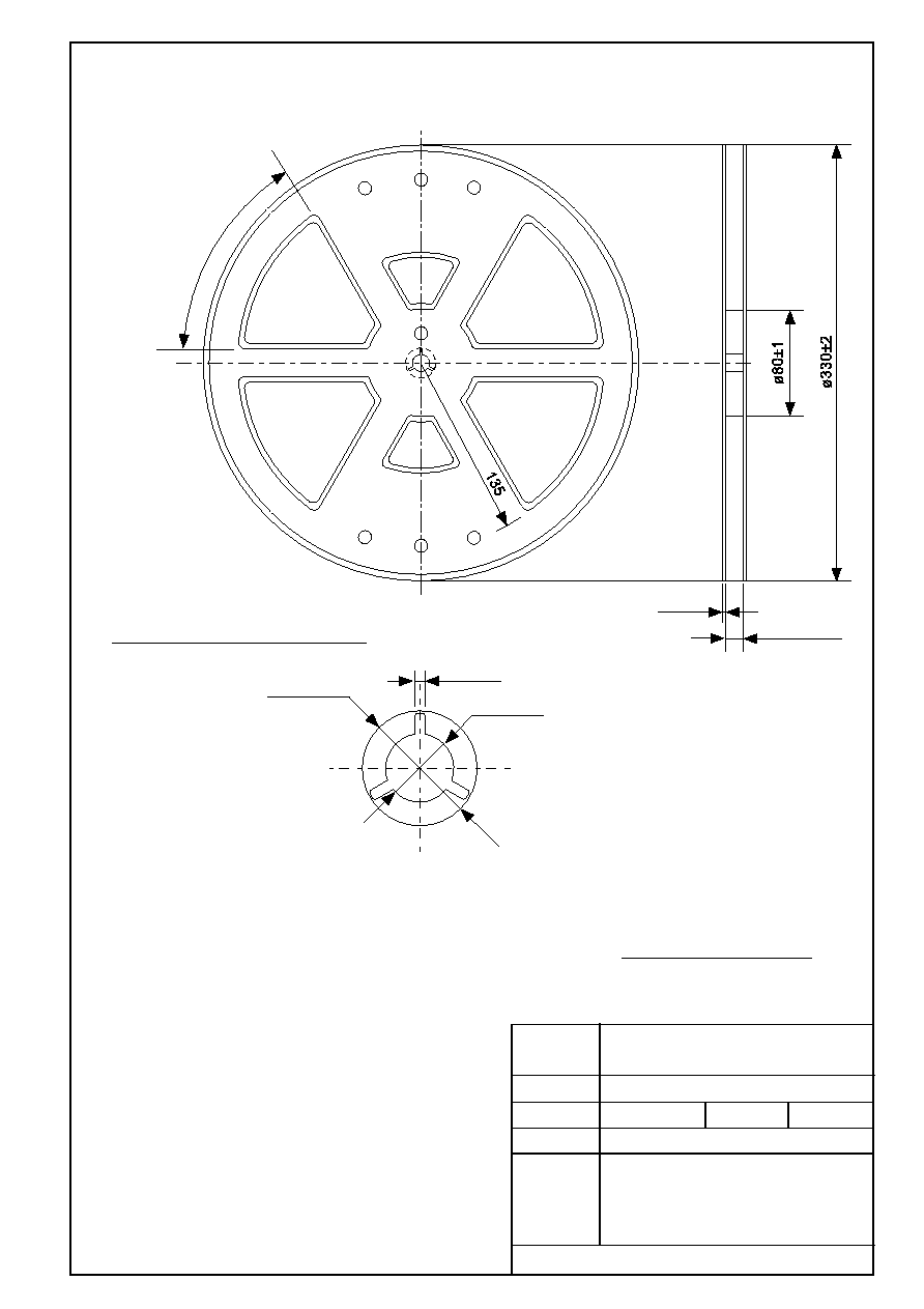
Seiko Instruments Inc.
Enlarged drawing in the central part
SOP8J-D-Reel
No. FJ008-D-R-SD-1.1
FJ008-D-R-SD-1.1
No.
TITLE
SCALE
UNIT
mm
Seiko Instruments Inc.
0.17±0.05
3.00
+0.3
-0.2
0.65
0.2±0.1
1
4
5
8
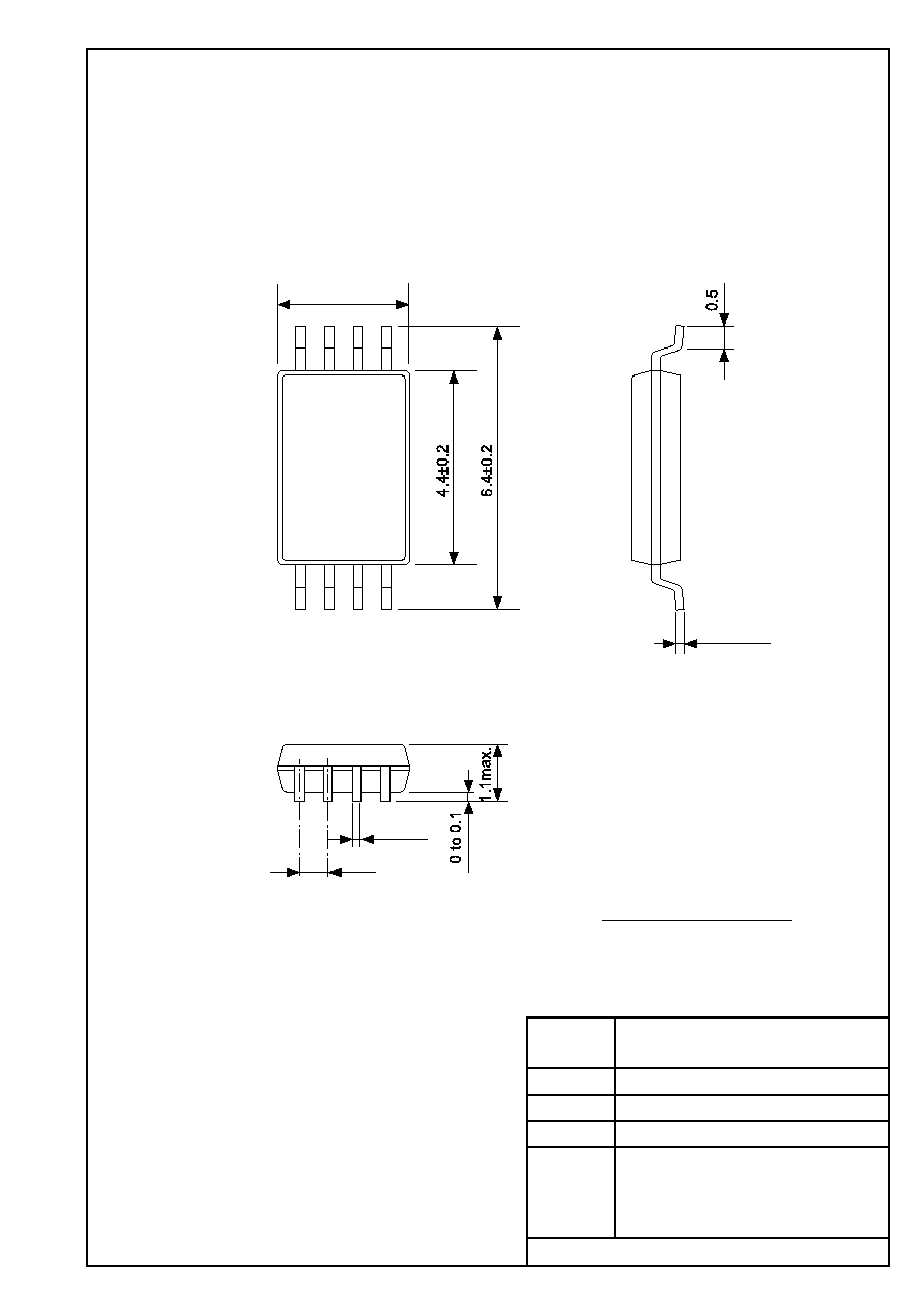
TSSOP8-A-PKG Dimensions
No. FT008-A-P-SD-1.1
FT008-A-P-SD-1.1
No.
TITLE
SCALE
UNIT
mm
Seiko Instruments Inc.
¯1.5
2.0±0.05
8.0±0.1
¯1.5
+0.1
-0
6.9±0.1
4.4±0.2
0.3±0.05
1
4
5
8
4.0±0.1
Feed direction
TSSOP8-D-Carrier Tape
No. FT008-D-C-SD-1.0
FT008-D-C-SD-1.0
+0.1
-0
No.
TITLE
SCALE
UNIT
mm
Seiko Instruments Inc.
QTY.
3,000
Enlarged drawing in the central part
TSSOP8-D-Reel
No. FT008-D-R-SD-1.0
FT008-D-R-SD-1.0
2±0.5
13.5±0.5
60∞
2±0.5
¯13±0.2
¯21±0.8

∑
The information described herein is subject to change without notice.
∑
Seiko Instruments Inc. is not responsible for any problems caused by circuits or diagrams described herein
whose related industrial properties, patents, or other rights belong to third parties. The application circuit
examples explain typical applications of the products, and do not guarantee the success of any specific
mass-production design.
∑
When the products described herein are regulated products subject to the Wassenaar Arrangement or other
agreements, they may not be exported without authorization from the appropriate governmental authority.
∑
Use of the information described herein for other purposes and/or reproduction or copying without the
express permission of Seiko Instruments Inc. is strictly prohibited.
∑
The products described herein cannot be used as part of any device or equipment affecting the human
body, such as exercise equipment, medical equipment, security systems, gas equipment, or any apparatus
installed in airplanes and other vehicles, without prior written permission of Seiko Instruments Inc.
∑
Although Seiko Instruments Inc. exerts the greatest possible effort to ensure high quality and reliability, the
failure or malfunction of semiconductor products may occur. The user of these products should therefore
give thorough consideration to safety design, including redundancy, fire-prevention measures, and
malfunction prevention, to prevent any accidents, fires, or community damage that may ensue.