
Contents
Features .................................................................................1
Pin Assignment......................................................................1
Pin Functions .........................................................................1
Block Diagram .......................................................................2
Instruction Set........................................................................2
Absolute Maximum Ratings ..................................................2
Recommended Operating Conditions....................................3
Pin Capacitance.....................................................................3
Endurance ..............................................................................3
DC Electrical Characteristics ................................................4
AC Electrical Characteristics.................................................5
Operation ................................................................................6
Receiving a Start-bit .......................................................... 13
Three-wire Interface (DI-DO direct connection ................... 13
Memory Protection................................................................13
Characteristics ......................................................................14
Ordering Information.............................................................19
Dimensions ...........................................................................20

Seiko Instruments Inc.
1
The S-29XX1A Series is high speed, low power 1K/2K/4K-bit E
2
PROM
with a wide operating voltage range. They are organized as 64-word
◊
16-bit, 128-word
◊
16-bit and 256-word
◊
16-bit, respectively. Each is
capable of sequential read, at which time addresses are automatically
incremented in 16-bit blocks. The instruction code is compatible with the
NM93CSXX Series.
The S-29XX1A Series is capable of protecting the memory, 50% of
which can be protected starting from address 00.
n
Pin Assignment
n
Pin Functions
Pin Number
Name
DIP
SOP1
Function
CS
1
3
Chip select input
SK
2
4
Serial clock input
DI
3
5
Serial data input
DO
4
6
Serial data output
GND
5
7
Ground
PROTECT
6
8
Memory Protection Control Input
Connected to GND or Open : Protection Valid
Connected to Vcc
: Protection Invalid
NC
7
1
No Connection
V
CC
8
2
Power supply
CMOS SERIAL E
2
PROM
S-29XX1A Series
n
Features
Low power consumption
Standby : 1.0
µ
A Max. (VCC=6.5 V)
Operating: 0.8 mA Max. (VCC=5.5 V)
: 0.4 mA Max. (VCC=2.5 V)
Wide operating voltage range
Write
: 2.5 to 6.5 V
Read
: 1.8 to 6.5 V
Memory Protection
Endurance : 10
5
cycles/word
Data retention : 10 years
S-29131A : 1K bits NM93CS46 instruction code compatible
S-29221A : 2K bits NM93CS56 instruction code compatible
S-29231A : 2K bits CAT35C102 instruction code compatible
S-29331A : 4K bits NM93CS66 instruction code compatible
Figure 1
NC
8-pin SOP1
Top view
PROTECT
GND
DO
DI
SK
6
5
8
7
V
CC
DO
NC
PROTECT
SK
DI
GND
CS
8-pin DIP
Top view
1
2
3
4
5
6
7
8
V
CC
CS
S-29131ADP
S-29221ADP
S-29231ADP
S-29331ADP
S-29131AFJ
S-29221AFJ
S-29231AFJ
S-29331AFJ
3
4
1
2
*
differs depending on the package type :
A : A type, (blank) : B type
See
n
Dimensions.
Table 1
Rev.1.1
CMOS SERIAL E
2
PROM
S-29XX1A Series
2
Seiko Instruments Inc.
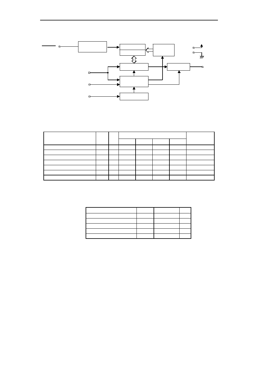
n
Block Diagram
n
Instruction Set
Table 2
Address
Instruction
Start
Bit
Op
code
S-29131A
S-29231A
S-29221A
S-29331A
Data
READ (Read data)
1
10
A
5
to A
0
A
6
to A
0
XA
6
to A
0
A
7
to A
0
D
15
to D
0
Output*
WRITE (Write data)
1
01
A
5
to A
0
A
6
to A
0
XA
6
to A
0
A
7
to A
0
D
15
to D
0
Input
ERASE (Erase data)
1
11
A
5
to A
0
A
6
to A
0
XA
6
to A
0
A
7
to A
0
--
WRAL (Write all)
1
00
01xxxx
01xxxxx
01xxxxxx
01xxxxxx
D
15
to D
0
Input
ERAL (Erase all)
1
00
10xxxx
10xxxxx
10xxxxxx
10xxxxxx
--
EWEN (Program enable)
1
00
11xxxx
11xxxxx
11xxxxxx
11xxxxxx
--
EWDS (Program disable)
1
00
00xxxx
00xxxxx
00xxxxxx
00xxxxxx
--
x : Doesn't matter.
* : Addresses are continuously incremented.
n
Absolute Maximum Ratings
Parameter
Symbol
Ratings
Unit
Power supply voltage
V
CC
-0.3 to +7.0
V
Input voltage
V
IN
-0.3 to V
CC
+0.3
V
Output voltage
V
OUT
-0.3 to V
CC
V
Storage temperature under bias
T
bias
-50 to +95
∞
C
Storage temperature
T
stg
-65 to +150
∞
C
Figure 2
Data register
Address
decoder
Mode decode
logic
Clock generator
Output buffer
V
CC
GND
DO
DI
CS
SK
Memory array
PROTECT
* 50% of the memory can be protected starting from address 00
Bank 1*
Bank 2
Write Protection
Circuit
Table 3

CMOS SERIAL E
2
PROM
S-29XX1A Series
Seiko Instruments Inc.
3
n
Recommended Operating Conditions
Table
4
Parameter
Symbol
Conditions
Min.
Typ.
Max.
Unit
Read Operation
Write Enable/Disable
1.8
--
6.5
V
Power supply voltage
V
CC
Write Operation
2.5
--
6.5
V
V
CC
=5.5 to 6.5 V
0.8
◊
Vcc
--
Vcc
V
V
CC
=4.5 to 5.5 V
2.0
--
Vcc
V
V
CC
=2.7 to 4.5 V
0.8
◊
Vcc
--
Vcc
V
High level input voltage
V
IH
V
CC
=1.8 to 2.7 V
0.8
◊
Vcc
--
Vcc
V
V
CC
=5.5 to 6.5 V
0.0
--
0.2
◊
Vcc
V
V
CC
=4.5 to 5.5 V
0.0
--
0.8
V
V
CC
=2.7 to 4.5 V
0.0
--
0.2
◊
Vcc
V
Low level input voltage
V
IL
V
CC
=1.8 to 2.7 V
0.0
--
0.15
◊
Vcc
V
Operating temperature
T
opr
-40
--
+85
∞
C
n
Pin Capacitance
Table 5
(Ta=25
∞
C, f=1.0 MHz, V
CC
=5 V)
Parameter
Symbol
Conditions
Min.
Typ.
Max.
Unit
Input Capacitance
C
IN
V
IN
=0 V
--
--
8
pF
Output Capacitance
C
OUT
V
OUT
=0 V
--
--
10
pF
n
Endurance
Table 6
Parameter
Symbol
Min.
Typ.
Max.
Unit
Endurance
N
W
10
5
--
--
cycles/word

CMOS SERIAL E
2
PROM
S-29XX1A Series
4
Seiko Instruments Inc.
n
DC Electrical Characteristics
V
CC
=5.5 V to 6.5
V
V
CC
=4.5 V to 5.5
V
V
CC
=2.5 to 4.5
V
VCC=1.8 to 2.5 V
Parameter
Smbl
Conditions
Min.
Typ.
Max.
Min.
Typ.
Max.
Min.
Typ.
Max.
Min.
Typ.
Max.
Unit
Current
consumption
(READ)
I
CC1
DO unloaded
--
--
1.0
--
--
0.8
--
--
0.6
--
--
0.4
mA
Current
consumption
(PROGRAM)
I
CC2
DO unloaded
--
--
2.5
--
--
2.0
--
--
1.5
mA
V
CC
=4.5 V to 6.5 V
V
CC
=2.5 to 4.5 V
V
CC
=1.8 to 2.5 V
Parameter
Smbl
Conditions
Min.
Typ. Max.
Min.
Typ. Max.
Min.
Typ. Max.
Unit
Standby current
consumption
I
SB
CS=GND DO=Open
Connected to V
CC
or GND
--
--
1.0
--
--
0.6
--
--
0.4
µ
A
Input leakage
current
I
LI
V
IN
=GND to V
CC
--
0.1
1.0
--
0.1
1.0
--
0.1
1.0
µ
A
Output leakage
current
I
LO
V
OUT
=GND to V
CC
--
0.1
1.0
--
0.1
1.0
--
0.1
1.0
µ
A
I
OL
=2.1 mA
--
--
0.45
V
Low level output
voltage
V
OL
I
OL
=100
µ
A
--
--
0.1
--
--
0.1
--
--
0.1
V
I
OH
=-400
µ
A
2.4
--
--
V
I
OH
=-100
µ
A
V
CC
-
0.7
--
--
V
CC
-
0.7
--
--
V
High level output
voltage
V
OH
I
OH
=-10
µ
A
V
CC
-
0.7
--
--
V
CC
-
0.7
--
--
V
CC
-
0.3
--
--
V
Write enable latch
data hold voltage
V
DH
Only when write disable
mode
1.5
--
--
1.5
--
--
1.5
--
--
V
Pull-Down Current
I
PD
PROTECT Terminal=V
CC
15
--
100
3
--
50
1
--
10
µ
A
Table
7
Table
8
CMOS SERIAL E
2
PROM
S-29XX1A Series
Seiko Instruments Inc.
5
n
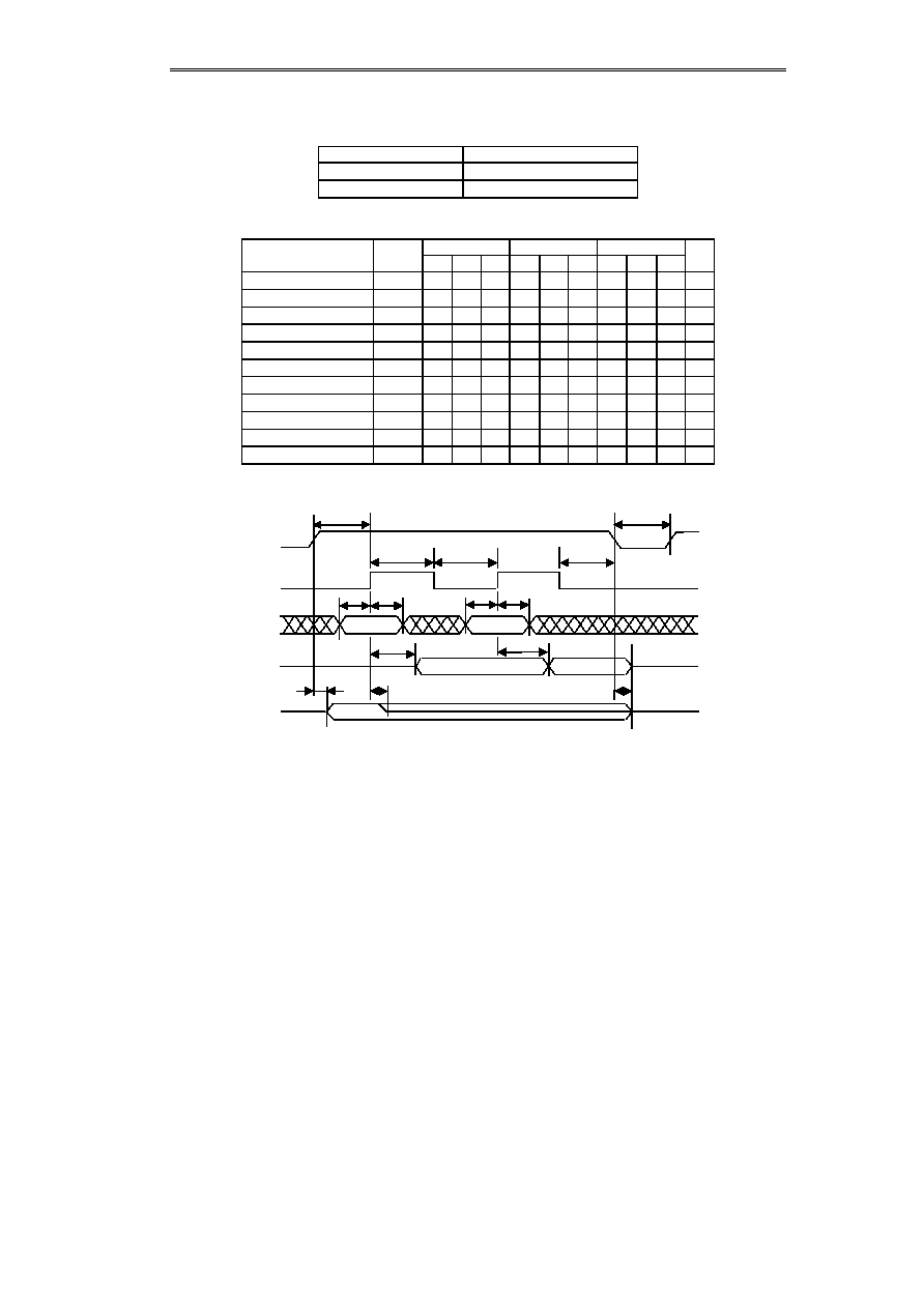
AC Electrical Characteristics
Table 9
Input pulse voltage
0.1
◊
V
CC
to 0.9
◊
V
CC
Output reference voltage
0.5
◊
V
CC
Output load
100pF
Table 10
V
CC
=4.5 to 6.5V
V
CC
=2.5 to 4.5 V
V
CC
=1.8 to 2.5V
Parameter
Smbl
Min. Typ. Max. Min. Typ. Max. Min.
Typ. Max.
Unit
CS setup time
t
CSS
0.2
--
--
0.4
--
--
1.0
--
--
µ
s
CS hold time
t
CSH
0.2
--
--
0.4
--
--
1.0
--
--
µ
s
CS deselect time
t
CDS
0.2
--
--
0.2
--
--
0.4
--
--
µ
s
Data setup time
t
DS
0.2
--
--
0.4
--
--
0.8
--
--
µ
s
Data hold time
t
DH
0.2
--
--
0.4
--
--
0.8
--
--
µ
s
Output delay
t
PD
--
--
0.4
--
--
1.0
--
--
2.0
µ
s
Clock frequency
f
SK
0
--
2.0
0
--
0.5
--
--
0.25 MHz
Clock pulse width
t
SKH,
t
SKL
0.25
--
--
1.0
--
--
2.0
--
--
µ
s
Output disable time
t
HZ1
,
t
HZ2
0
--
0.15
0
--
0.5
0
--
1.0
µ
s
Output enable time
t
SV
0
--
0.15
0
--
0.5
0
--
1.0
µ
s
Programming time
t
PR
--
4.0
10.0
--
4.0
10.0
ms
Figure 3
Timing Chart
t
SKH
t
CDS
t
CSS
CS
Valid data
Valid data
DI
t
SKL
SK
t
SV
t
HZ2
t
CSH
t
HZ1
t
PD
t
PD
t
DS
t
DH
t
DS
t
DH
Hi-Z
Hi-Z
Hi-Z
DO
DO
(READ)
(VERIFY)
Hi-Z

CMOS SERIAL E
2
PROM
S-29XX1A Series
6
Seiko Instruments Inc.
n
Operation
Instructions (in the order of start-bit, instruction, address, and data) are latched to DI in synchronization with the
rising edge of SK after CS goes high. A start-bit can only be recognized when the high of DI is latched to the rising
edge of SK when CS goes from low to high, it is impossible for it to be recognized as long as DI is low, even if there
are SK pulses after CS goes high. Any SK pulses input while DI is low are called "dummy clocks." Dummy clocks
can be used to adjust the number of clock cycles needed by the serial IC to match those sent out by the CPU.
Instruction input finishes when CS goes low, where it must be between commands during t
CDS
.
All input, including DI and SK signals, is ignored while CS is low, which is stand-by mode.
1.
Read
The READ instruction reads data from a specified address. After A0 is latched at the rising edge of SK, DO output
changes from a high-impedance state (Hi-Z) to low level output. Data is continuously output in synchronization with
the rise of SK.
When all of the data (D0) in the specified address has been read, the data in the next address can be read with the
input of another SK clock. Thus, it is possible for all of the data addresses to be read through the continuous input
of SK clocks as long as CS is high.
The last address (An ... A1 A0 = 1 ... 11) rolls over to the top address (An ... A0 = 0 ... 00).
Figure 4
Read Timing (S-29131A)
D
15
D
15
D
14
D
14
D
13
D
14
Hi
-
Z
A
5
A
4
A
3
A
2
A
1
A
0
+1
D
13
D
0
D
1
D
2
D
15
0
Hi-Z
A
0
A
1
A
2
A
3
A
4
A
5
0
1
1
28
27
26
25
24
23
12
11
10
9
8
7
6
5
4
3
2
1
44
43
42
41
40
39
A
5
A
4
A
3
A
2
A
1
A
0
+2
D
13
D
0
D
1
D
2
CS
SK
DI
DO
Figure 5
Read Timing
(S-29231A)
4
0
1
1
3
2
1
CS
SK
DI
DO
D
15
D
15
D
14
D
14
D
13
D
14
Hi
-
Z
A
6
A
5
A
4
A
3
A
2
A
1
A
0
+1
D
13
D
0
D
1
D
2
D
15
0
Hi-Z
A
0
A
1
A
2
A
3
A
4
A
5
29
28
27
26
25
24
13
12
11
10
9
8
7
6
5
45
44
43
42
41
40
A
6
A
5
A
4
A
3
A
2
A
1
A
0
+2
D
13
D
0
D
1
D
2
A
6

CMOS SERIAL E
2
PROM
S-29XX1A Series
Seiko Instruments Inc.
7
A
0
A
6
12
45
29
14
D
15
D
15
D
14
D
14
D
13
D
14
Hi
-
Z
A
6
A
5
A
4
A
3
A
2
A
1
A
0
+1
D
13
D
0
D
1
D
2
D
15
0
Hi-Z
A
1
A
2
A
3
A
4
A
5
X
0
1
1
28
27
26
25
24
11
10
9
8
7
6
5
4
3
2
1
44
43
42
41
40
A
6
A
5
A
4
A
3
A
2
A
1
A
0
+2
D
13
D
0
D
1
D
2
13
CS
SK
DI
DO
Figure 6
Read Timing
(S-29221A)
A
0
A
6
12
45
29
14
D
15
D
15
D
14
D
14
D
13
D
14
Hi
-
Z
A
7
A
6
A
5
A
4
A
3
A
2
A
1
A
0
+1
D
13
D
0
D
1
D
2
D
15
0
Hi-Z
A
1
A
2
A
3
A
4
A
5
A
7
0
1
1
28
27
26
25
24
11
10
9
8
7
6
5
4
3
2
1
44
43
42
41
40
A
7
A
6
A
5
A
4
A
3
A
2
A
1
A
0
+2
D
13
D
0
D
1
D
2
13
CS
SK
DI
DO
Figure 7
Read Timing
(S-29331A)
2. WRITE (WRITE, ERASE, WRAL, ERAL)
There are four write instructions, WRITE, ERASE, WRAL, and ERAL. Each automatically begins writing to the non-
volatile memory when CS goes low at the completion of the specified clock input.
The write operation is completed in 10 ms (t
PR
Max.), and the typical write period is less than 5 ms. In the S-
29XX1A Series, it is easy to VERIFY the completion of the write operation in order to minimize the write cycle by
setting CS to high and checking the DO pin, which is low during the write operation and high after its completion.
This VERIFY procedure can be executed over and over again.
Because all SK and DI inputs are ignored during the write operation, any input of instruction will also be
disregarded. When DO outputs high after completion of the write operation or if it is in the high-impedence state
(Hi-Z), the input of instructions is available. Even if the DO pin remains high, it will enter the high-impedence state
upon the recognition of a high of DI (start-bit) attached to the rising edge of an SK pulse. (see Figure 3).
DI input should be low during the VERIFY procedure.

CMOS SERIAL E
2
PROM
S-29XX1A Series
8
Seiko Instruments Inc.
2.1 WRITE
This instruction writes 16-bit data to a specified address.
After changing CS to high, input a start-bit, op-code (WRITE), address, and 16-bit data. If there is a data overflow of more than
16 bits, only the last 16-bits of the data is considered valid. Changing CS to low will start the WRITE operation. It is not
necessary to make the data "1" before initiating the WRITE operation.
Figure 8
WRITE Timing (S-29131A)
t
CDS
t
PR
busy
Hi-Z
t
SV
VERIFY
Hi-Z
1
CS
SK
DI
DO
t
HZ1
2
3
4
5
6
7
8
9
10
25
∑
0
1
D0
ready
A5
A4
A3
A2
A1
A0
D15
Figure 9
WRITE Timing (S-29231A)
Hi-Z
CS
DO
DI
∑
0
1
A6
t
CDS
t
PR
busy
Hi-Z
t
SV
VERIFY
t
HZ1
8
9
10
11
26
D0
ready
A3
A2
A1
A0
D15
6
7
1
SK
2
3
4
5
A5
A4
Figure 10
WRITE Timing (S-29221A)
t
CDS
t
PR
busy
Hi-Z
t
SV
VERIFY
Hi-Z
1
CS
SK
DI
DO
t
HZ1
2
3
4
5
6
7
8
9
10
11
12
27
∑
0
1
D0
ready
X
A6
A5
A4
A3
A2
A1
A0
D15
Figure 11
WRITE Timing (S-29331A)
t
CDS
t
PR
busy
Hi-Z
t
SV
VERIFY
Hi-Z
1
CS
SK
DI
DO
t
HZ1
2
3
4
5
6
7
8
9
10
11
12
27
∑
0
1
D0
ready
A7
A6
A5
A4
A3
A2
A1
A0
D15

CMOS SERIAL E
2
PROM
S-29XX1A Series
Seiko Instruments Inc.
9
2.2 ERASE
This command erases 16-bit data in a specified address.
After changing CS to high, input a start-bit, op-code (ERASE), and address. It is not necessary to input data.
Changing CS to low will start the ERASE operation, which changes every bit of the 16 bit data to "1."
Figure 12
ERASE Timing (S-29131A)
t
CDS
t
PR
busy
Hi-Z
t
SV
VERIFY
Hi-Z
1
CS
SK
DI
DO
t
HZ1
2
3
4
5
6
7
8
9
∑
1
A0
ready
1
A5
A4
A3
A2
A1
Figure 13
ERASE Timing (S-29231A)
Hi-Z
CS
DI
DO
1
∑
1
t
CDS
t
PR
busy
Hi-Z
t
SV
VERIFY
t
HZ1
5
6
7
8
9
10
A0
ready
A5
A4
A3
A2
A1
1
SK
2
3
4
A6
Figure 14
ERASE Timing (S-29221A)
t
CDS
t
PR
busy
Hi-Z
t
SV
VERIFY
Hi-Z
1
CS
SK
DI
DO
t
HZ1
2
3
4
5
6
7
8
9
10
11
¨
1
A0
ready
1
X
A6
A5
A4
A3
A2
A1
Figure 15
ERASE Timing (S-29331A)
t
CDS
t
PR
busy
Hi-Z
t
SV
VERIFY
Hi-Z
1
CS
SK
DI
DO
t
HZ1
2
3
4
5
6
7
8
9
10
11
∑
1
A0
ready
1
A7
A6
A5
A4
A3
A2
A1

CMOS SERIAL E
2
PROM
S-29XX1A Series
10
Seiko Instruments Inc.
2.3
WRAL
This instruction writes the same 16-bit data into every address.
After changing CS to high, input a start-bit, op-code (WRAL), address (optional), and 16-bit data. If there is a data
overflow of more than 16 bits, only the last 16-bits of the data is considered valid. Changing CS to low will start the
WRAL operation. It is not necessary to make the data "1" before initiating the WRAL operation.
Figure 16
WRAL Timing (S-29131A)
t
CDS
t
PR
busy
Hi-Z
t
SV
VERIFY
Hi-Z
1
CS
SK
DI
DO
t
HZ1
2
3
4
5
6
7
8
9
10
25
∑
0
D0
ready
0
0
1
4Xs
D15
Figure 17
WRAL Timing (S-29231A)
Hi-Z
1
CS
SK
DI
DO
2
3
4
5
6
7
8
9
∑
0
0
0
1
5Xs
t
CDS
t
PR
busy
Hi-Z
t
SV
t
HZ1
11
26
D0
ready
D15
10
VERIFY
Figure 18
WRAL Timing (S-29221A)
t
CDS
t
PR
busy
Hi-Z
t
SV
VERIFY
Hi-Z
1
CS
SK
DI
DO
t
HZ1
2
3
4
5
6
7
8
9
10
11
12
27
∑
0
D0
ready
0
0
1
6Xs
D15
Figure 19
WRAL Timing (S-29331A)
t
CDS
t
PR
busy
Hi-Z
t
SV
VERIFY
Hi-Z
1
CS
SK
DI
DO
t
HZ1
2
3
4
5
6
7
8
9
10
11
12
27
∑
0
D0
ready
0
0
1
6Xs
D15

CMOS SERIAL E
2
PROM
S-29XX1A Series
Seiko Instruments Inc.
11
2.4 ERAL
This instruction erases the data in every address.
After changing CS to high, input a start-bit, op-code (ERAL), and address (optional). It is not necessary to input data.
Changing CS to low will start the ERAL operation, which changes every bit of data to "1."
Figure 20
ERAL Timing (S-29131A)
t
CDS
4Xs
0
1
0
8
7
6
5
4
3
2
1
CS
SK
DI
DO
∑
0
t
PR
Hi-Z
t
HZ1
ready
busy
t
SV
VERIFY
9
Figure 21
ERAL Timing (S-29231A)
5Xs
0
1
0
8
7
6
5
4
3
2
1
CS
SK
DI
DO
∑
0
t
CDS
t
PR
Hi-Z
t
HZ1
ready
busy
t
SV
VERIFY
10
9
Figure 22
ERAL Timing (S-29221A)
11
t
CDS
6Xs
0
1
0
8
7
6
5
4
3
2
1
CS
SK
DI
DO
∑
0
t
PR
Hi-Z
t
HZ1
ready
busy
t
SV
VERIFY
10
9
Figure 23
ERAL Timing (S-29331A)
11
t
CDS
6Xs
0
1
0
8
7
6
5
4
3
2
1
CS
SK
DI
DO
∑
0
t
PR
Hi-Z
t
HZ1
ready
busy
t
SV
VERIFY
10
9

CMOS SERIAL E
2
PROM
S-29XX1A Series
12
Seiko Instruments Inc.
3.
Write enable (EWEN) and Write disable (EWDS)
The EWEN instruction puts the S-29XX1A Series into write enable mode, which accepts WRITE, ERASE, WRAL, and
ERAL instructions. The EWDS instruction puts the S-29XX1A Series into write disable mode, which refuses WRITE,
ERASE, WRAL, and ERAL instructions.
The S-29XX1A Series powers on in write disable mode, which protects data against unexpected, erroneous write
operations caused by noise and/or CPU malfunctions. It should be kept in write disable mode except when
performing write operations.
Figure 24
EWEN/EWDS Timing (S-29131A)
4Xs
11=EWEN
00=EWDS
0
8
7
6
5
4
3
2
1
SK
DI
∑
0
9
CS
Figure 25
EWEN/EWDS Timing (S-29231A)
5Xs
11=EWEN
00=EWDS
0
8
7
6
5
4
3
2
1
SK
DI
∑
0
CS
10
9
Figure 26
EWEN/EWDS Timing (S-29221A)
6Xs
11=EWEN
00=EWDS
0
8
7
6
5
4
3
2
1
SK
DI
∑
0
11
9
CS
10
Figure 27
EWEN/EWDS Timing (S-29331A)
6Xs
11=EWEN
00=EWDS
0
8
7
6
5
4
3
2
1
SK
DI
∑
0
11
9
CS
10

CMOS SERIAL E
2
PROM
S-29XX1A Series
Seiko Instruments Inc.
13
n
Receiving a Start-Bit
Both the recognition of a start-bit and the VERIFY procedure occur when CS is "high." Therefore, only after a write
operation, in order to accept the next command by having CS go high, will the DO pin switch from a state of high-
impedence to a state of data output; but if it recognizes a start-bit, the DO pin returns to a state of high-impedence.
n
Three-wire Interface (DI-DO direct connection)
Although the normal configuration of a serial interface is a 4-wire interface to CS, SK, DI, and DO, a 3-wire interface is
also a possibility by connecting DI and DO. However, since there is a possibility that the DO output from the serial
memory IC will interfere with the data output from the CPU with a 3-wire interface, install a resistor between DI and
DO in order to give preference to data output from the CPU to DI(See Figure 28).
n
Memory Protection
DI
SIO
Figure 28
DO
CPU
S-29XX1A
R : 10 to 100 k
Figure 29 PROTECT Terminal Input Signal Timing
The S-29XX1A Series is capable of protecting the memory. So, the contents of the memory will not be miswritten
due to error run or malfunction of the CPU. When the PROTECT terminal is connected to GND or OPEN, write to
Bank 1 in the memory array is prohibited (50% of the memory can be protected starting from address 00). Because
the pull-down resistance is connected to the PROTECT terminal internally, the memory can be automatically
protected when the PROTECT terminal is OPEN. When the protection is valid, the data in the memory of Bank 1
will not be rewritten. However, because the write control circuit inside the IC functions, the next instruction cannot
be executed during the time period of writing (t
PR
). While write instruction is being input and write is being
executed, always connect the PROTECT terminal to " H, " " L" or OPEN, and leave the input signal unchanged (see
Figure 29).
CS
Verify
Write Instruction Input
DO
busy
Hi-Z
Hi-Z
ready
t
PR
0.2
µ
s Min.
0.2
µ
s Min.
PROTECT
DI
SK

CMOS SERIAL E
2
PROM
S-29XX1A Series
14
Seiko Instruments Inc.
n
Characteristics
1. DC Characteristics
Ta (
∞
C)
0.4
0.2
V
CC
=5.5 V
f
SK
=2 MHz
DATA=0101
0
-40
0
85
I
CC1
(mA)
Ta (
∞
C)
0.4
0.2
V
CC
=3.3 V
f
SK
=500 KHz
DATA=0101
0
-40
0
85
I
CC1
(mA)
Ta (
∞
C)
0.4
0.2
V
CC
=1.8 V
f
SK
=10 KHz
DATA=0101
0
-40
0
85
I
CC1
(mA)
0.4
0.2
0
2
3
4
5 6
7
Ta=25
∞
C
f
SK
=1 MHz, 500 KHz
DATA=0101
V
CC
(V)
0.4
0.2
0
2
3
4
5 6
7
Ta=25
∞
C
f
SK
=100 KHz, 10 KHz
DATA=0101
V
CC
(V)
0.4
0.2
0
I
CC1
(mA)
V
CC
=5.0 V
Ta=25
∞
C
1M 2M
10K 100K
f
SK
(Hz)
Ta (
∞
C)
1.0
0.5
V
CC
=5.5 V
0
-40
0
85
I
CC2
(mA)
Ta (
∞
C)
1.0
0.5
V
CC
=3.3 V
0
-40
0
85
I
CC2
(mA)
I
CC1
(mA)
I
CC1
(mA)
100KHZ
~
10KH
Z
~
1MHZ
~
~
500KH
Z
1.1 Current consumption (READ) I
CC1
--
Ambient temperature Ta
1.2 Current consumption (READ) I
CC1
--
Ambient temperature Ta
1.3 Current consumption (READ) I
CC1
--
Ambient temperature Ta
1.4 Current consumption (READ) I
CC1
--
Power supply voltage V
CC
1.5 Current consumption (READ) I
CC1
--
Power supply voltage V
CC
1.6 Current consumption (READ) I
CC1
--
Clock frequency f
SK
1.7 Current consumption (PROGRAM) I
CC2
-
Ambient temperature Ta
1.8 Current consumption (PROGRAM) I
CC2
-
Ambient temperature Ta

CMOS SERIAL E
2
PROM
S-29XX1A Series
Seiko Instruments Inc.
15
40
20
0
2
3
4
5 6
7
Ta=25
∞
C
V
CC
(V)
Ta (
∞
C)
1.0
0.5
V
CC
=5.5 V
DO=0 V
0
-40
0
85
I
LO
(
µ
A)
Ta (
∞
C)
1.0
0.5
V
CC
=5.5 V
DO=5.5 V
0
-40
0
85
I
LO
(
µ
A)
I
PD
(
µ
A)
Ta (
∞
C)
1.0
0.5
V
CC
=5.5 V
CS, SK, DI,
TEST=0 V
0
-40
0
85
I
LI
(
µ
A)
Ta (
∞
C)
1.0
0.5
0
-40
0
85
V
CC
=5.5 V
CS, SK, DI,
TEST=5.5 V
I
LI
(
µ
A)
1.0
0.5
0
2
3
4
5 6
7
Ta=25
∞
C
V
CC
(V)
I
CC2
(mA)
10
-6
10
-7
10
-8
10
-9
10
-10
V
CC
=5.5 V
10
-11
Ta (
∞
C)
-40
0
85
I
SB
(A)
Ta (
∞
C)
4.6
4.4
V
CC
=4.5 V
I
OH
=-400
µ
A
-40
0
85
V
OH
(V)
4.2
1.9
Current consumption (PROGRAM) I
CC2
-
Power supply voltage V
CC
1.10 Standby current consumption I
SB
--
Ambient temperature Ta
1.11 Pull-Down current I
PD
--
Power supply voltageV
CC
1.12 Input leakage current I
LI
-
Ambient temperature Ta
1.13 Input leakage current I
LI
-
Ambient temperature Ta
1.14 Output leakage current I
LO
-
Ambient temperature Ta
1.15 Output leakage current I
LO
-
Ambient temperature Ta
1.16 High level output voltage V
OH
-
Ambient temperature Ta

CMOS SERIAL E
2
PROM
S-29XX1A Series
16
Seiko Instruments Inc.
Ta (
∞
C)
2.7
2.6
V
CC
=2.7 V
I
OH
=-100
µ
A
-40
0
85
V
OH
(V)
2.5
Ta (
∞
C)
2.5
2.4
V
CC
=2.5 V
I
OH
=-100
µ
A
-40
0
85
V
OH
(V)
2.3
Ta (
∞
C)
0.3
0.2
V
CC
=4.5 V
I
OL
=2.1 mA
-40
0
85
V
OL
(V)
0.1
Ta (
∞
C)
0.03
0.02
V
CC
=1.8 V
I
OL
=100
µ
A
-40
0
85
V
OL
(V)
0.01
Ta (
∞
C)
-10.0
-5.0
V
CC
=4.5 V
V
OH
=2.4 V
0
-40
0
85
I
OH
(mA)
Ta (
∞
C)
-4
-2
V
CC
=2.7 V
V
OH
=2.0 V
0
-40
0
85
I
OH
(mA)
Ta (
∞
C)
-4
-2
V
CC
=2.5 V
V
OH
=1.8 V
0
-40
0
85
I
OH
(mA)
Ta (
∞
C)
20
10
V
CC
=4.5 V
V
OL
=0.45 V
0
-40
0
85
I
OL
(mA)
1.17 High level output voltage V
OH
-
Ambient temperature Ta
1.18 High level output voltage V
OH
-
Ambient temperature Ta
1.19 Low level output voltage V
OL
-
Ambient temperature Ta
1.20 Low level output voltage V
OL
-
Ambient temperature Ta
1.21 High level output current I
OH
-
Ambient temperature Ta
1.22 High level output current I
OH
-
Ambient temperature Ta
1.23 High level output current I
OH
-
Ambient temperature Ta
1.24 Low level output current I
OL
-
Ambient temperature Ta

CMOS SERIAL E
2
PROM
S-29XX1A Series
Seiko Instruments Inc.
17
Ta (
∞
C)
1.0
0.5
V
CC
=1.8 V
V
OL
=0.1 V
0
-40
0
85
I
OL
(mA)
Ta (
∞
C)
3.0
2.0
0
-40
0
85
3.0
1.5
0
1
2
3
4 5
6
Ta=25
∞
C
CS, SK, DI,
PROT
V
CC
(V)
V
INV
(V)
7
V
INV
(V)
V
CC
=5.0 V
CS, SK, DI,
PROT
1.25 Low level output current I
OL
-
Ambient temperature Ta
1.26 Input voltage V
IN
(V
IL
, V
IH
) -
Power supply voltage V
CC
1.27 Input voltage V
IN
(V
IL
, V
IH
) -
Ambient temperature Ta

CMOS SERIAL E
2
PROM
S-29XX1A Series
18
Seiko Instruments Inc.
2.
AC Characteristics
10K
2
3
4
5
Ta=25
∞
C
V
CC
(V)
f
max
(Hz)
1
4
2
2
3
4
5 6
7
Ta=25
∞
C
V
CC
(V)
t
PR
(ms)
1
100K
1M
2M
Ta (
∞
C)
6
4
V
CC
=5.0 V
-40
0
85
2
t
PR
(ms)
Ta (
∞
C)
6
4
V
CC
=3.0 V
-40
0
85
2
t
PR
(ms)
Ta (
∞
C)
0.6
0.4
V
CC
=1.8 V
-40
0
85
0.2
t
PD
(
µ
s)
Ta (
∞
C)
0.3
0.2
V
CC
=4.5 V
-40
0
85
0.1
t
PD
(
µ
s)
Ta (
∞
C)
0.6
0.4
V
CC
=2.7 V
-40
0
85
0.2
t
PD
(
µ
s)
2.1 Maximum operating frequency fmax ≠
Power supply voltage V
CC
2.2 Program time t
PR
≠
Power supply voltage V
CC
2.3 Program time t
PR
≠
Ambient temperature Ta
2.4 Program time t
PR
≠
Ambient temperature Ta
2.5 Data output delay time t
PD
≠
Ambient temperature Ta
2.6 Data output delay time t
PD
≠
Ambient temperature Ta
2.7 Data output delay time t
PD
-
Ambient temperature Ta

CMOS SERIAL E
2
PROM
S-29XX1A Series
Seiko Instruments Inc.
19
n
Ordering Information
1. 8-pin DIP
There are two types of packages : A or B.
2.
8-pin SOP
There are two types of packages : A or B.
A type
S-29131ADPA
S-29221ADPA
S-29231ADPA
S-29331ADPA
B type
S-29131ADP
S-29221ADP
S-29231ADP
S-29331ADP
A type
S-29131AFJA
S-29221AFJA
S-29231AFJA
S-29331AFJA
B type
S-29131AFJ
S-29221AFJ
S-29231AFJ
S-29331AFJ
S-29XX1A
XX
Package type
A
: A type
(blank)
: B type
Package
DP
: DIP
FJ
: SOP1
Product name
S-29131A
: 1K-bit
S-29221A
: 2K-bit
S-29231A
: 2K-bit
S-29331A
: 4K-bit
See
n
Pin Assignment, (Figure 1)

0.4±0.05
1.27
0.20±0.05
4.90(4.95max)
1
4
8
5
8-pin SOP
FJ008-A 990531
¯2.0±0.05
¯1.55±0.05
4.0±0.1(10 pitches 40.0 0.2)
0.3±0.05
2.1±0.1
8.0±0.1
6.7±0.1
2.0±0.05
5 max.
5
8
1
4
Feed direction
2±0.5
13.5±0.5
2±0.5
¯13±0.2
¯21±0.8
60∞
Winding core
Unit:mm
Dimensions
Taping Specifications
Reel Specifications
A type

0.42±0.09
1.27
0.22±0.03
4.90(5.00max)
1
4
8
5
8-pin SOP
FJ008-B 990531
¯2.0±0.05
¯1.55±0.05
1.75±0.1
4.0±0.1(10 pitches 40.0±0.2)
0.3±0.05
2.1±0.1
8.0±0.1
6.7±0.1
2.0±0.05
5 max.
3 max.
5
8
1
4
Feed direction
12.0±0.2
5.5±0.05
5.55±0.1
135
2±0.5
13.5±0.5
2±0.5
¯13±0.2
¯21±0.8
60∞
¯80±1
¯330±2
Winding core
Unit:mm
Dimensions
Taping Specifications
Reel Specifications
B type

DP00 -A 990531
0.5±0.1
2.54
1.0
1.5
0∞~15∞
0.3
+0.1
-0.05
7.62
9.3(9.6max)
8-pin DIP
Unit:mm
Dimensions
A type

0.46±0.05
2.54
0.99
1.52
1∞~10∞
7.87
9.50(9.76max)
0.25±0.05
DP008-B 990531
8-pin DIP
Dimensions
Unit:mm
B type

8-pin DIP Both type A and B
Markings
990603
29/24C01/08
8-pin SOP Both type A snd B
Numbers 1, 2, 7, 8, and/or 12
include blanks depending on
product type.
Numbers 1, 6, 7, and/or 11 include
blanks depending on product type.

∑
The information herein is subject to change without notice.
∑
Seiko Instruments Inc. is not responsible for any problems caused by circuits or other diagrams
described herein whose industrial properties, patents or other rights belong to third parties. The
application circuit examples explain typical applications of the products, and do not guarantee any
mass-production design.
∑
When the products described herein include Strategic Products (or Service) subject to regulations,
they should not be exported without authorization from the appropriate governmental authorities.
∑
The products described herein cannot be used as part of any device or equipment which influences
the human body, such as physical exercise equipment, medical equipment, security system, gas
equipment, vehicle or airplane, without prior written permission of Seiko Instruments Inc.