
Seiko Instruments Inc.
1
The S-29X94A Series is high speed, low power 1K/2K/4K-bit serial
E
2
PROM with a wide operating voltage range. They are organized as
64-word
◊
16-bit, 128-word
◊
16-bit and 256-word
◊
16-bit, respectively.
Each is capable of sequential read, where addresses are automatically
incremented in 16-bit blocks.
The S-29X94A Series is capable of protecting the memory, 50
%
of which
can be protected starting from address 00.
Interface is structured so that this IC can be directly connected to the CPU
with serial ports. 8-bit instructions make it easy to prepare your own
software.
Package
8-Pin DIP (PKG drawing code : DP008-A)
8-Pin SOP (PKG drawing code : FJ008-A)
Pin
Assignment
Figure 1
CMOS SERIAL E
2
PROM
S-29X94A Series
Features
∑
Low power consumption
Standby :
1.0
Ķ
A Max. (V
CC
=
6.5 V)
Operating : 0.8 mA Max. (V
CC
=
5.5 V)
0.4 mA Max. (V
CC
=
2.5 V)
∑
Wide operating voltage range
Write
:2.5 to 6.5 V
Read
:1.8 to 6.5 V
∑
Sequential read capable
∑
Memory Protection
8-Pin SOP1
Top view
8-Pin DIP
Top view
VCC
DO
NC
SK
DI
GND
1
2
3
4
5
6
7
8
VCC
GND
DO
DI
6
5
8
7
SK
NC
CS
PROTECT
CS
PROTECT
S-29194ADPA
S-29294ADPA
S-29394ADPA
S-29194AFJA
S-29294AFJA
S-29394AFJA
3
4
1
2
Rev.1.2
_20
∑
Can be easily connected to the serial port
∑
CS Active "L"
∑
Endurance : 10
5
cycles/word
∑
Data retention : 10 years
∑
S-29194A : 1 Kbits
∑
S-29294A : 2 Kbits
∑
S-29394A : 4 Kbits

CMOS SERIAL E
2
PROM
S-29X94A Series
2
Seiko Instruments Inc.
Pin
Functions
Table 1
Pin Number
Name
DIP SOP1
Function
CS
1 3
Chip select input
SK
2 4
Serial clock input
DI
3 5
Serial data input
DO
4 6
Serial data output
GND
5 7
Ground
PROTECT
6 8
Memory Protection Control Input
Connected to GND or Open : Protection Valid
Connected to Vcc
: Protection Invalid
NC
7 1
No Connection
VCC
8 2
Power supply
Block
Diagram
Instruction
Set
Table 2
Address
Instruction
Start
Bit
Ope
code
S-29194A S-29294A S-29394A
Data
READ (Read data)
1
1000xxx
xx A5toA0
x A6toA0
A7toA0
D
15
to D
0
Output*
PROGRAM (Program data)
1
x100xxx
xx A5toA0
x A6toA0
A7toA0
D
15
to D
0
Input
WRAL (Write all)
1
0001xxx
xxxxxxxx xxxxxxxx xxxxxxxx D
15
to D
0
Input
ERAL (Erase all)
1
0010xxx
xxxxxxxx xxxxxxxx xxxxxxxx
--
PEN (Program
enable)
1
0011xxx
xxxxxxxx xxxxxxxx xxxxxxxx
--
PDS (Program
disable)
1
0000xxx
xxxxxxxx xxxxxxxx xxxxxxxx
--
x : Doesn't matter.
* : When 16-bit data of the specified address is output, the data of the next address is output.
Figure 2
Data register
Address
decoder
Mode decode
logic
Clock generator
Output buffer
VCC
GND
DO
DI
CS
SK
Memory array
PROTECT
*50
%
of the memory can be protected starting from address 00.
Bank 1*
Bank 2
Write Protection
Circuit
CMOS SERIAL E
2
PROM
S-29X94A Series
Seiko Instruments Inc.
3
Absolute
Maximum
Ratings
Caution The absolute maximum ratings are rated values exceeding which
the product could suffer physical damage. These values must
therefore not be exceeded under any conditions.
Recommended
Operating
Conditions
Table 4
Parameter Symbol
Conditions Min.
Typ.
Max.
Unit
Read Operation
Write Enable/Disable
1.8 -- 6.5 V
Power supply voltage
V
CC
Write Operation
2.5
--
6.5
V
High level input voltage
V
IH
V
CC
=
5.5 to 6.5 V
V
CC
=
4.5 to 5.5 V
V
CC
=
2.7 to 4.5 V
V
CC
=
1.8 to 2.7 V
0.8
◊
Vcc
2.0
0.8
◊
Vcc
0.8
◊
Vcc
--
--
--
--
Vcc
Vcc
Vcc
Vcc
V
V
V
V
Low level input voltage
V
IL
V
CC
=
5.5 to 6.5 V
V
CC
=
4.5 to 5.5 V
V
CC
=
2.7 to 4.5 V
V
CC
=
1.8 to 2.7 V
0.0
0.0
0.0
0.0
--
--
--
--
0.2
◊
Vcc
0.8
0.2
◊
Vcc
0.15
◊
Vcc
V
V
V
V
Operating temperature
T
opr
--
-
40 --
+
85 įC
Pin Capacitance
Table 5
(Ta
=
25įC, f
=
1.0 MHz, V
CC
=
5 V)
Parameter Symbol
Conditions
Min.
Typ.
Max.
Unit
Input Capacitance
C
IN
V
IN
=
0 V
--
--
8
pF
Output Capacitance
C
OUT
V
OUT
=
0 V
--
--
10
pF
Endurance
Table 6
Parameter Symbol
Min.
Typ.
Max. Unit
Endurance N
W
10
5
-- --
cycles/word
Table 3
Parameter Symbol
Ratings
Unit
Power supply voltage
V
CC
-
0.3 to
+
7.0 V
Input voltage
V
IN
-
0.3 to V
CC
+
0.3 V
Output voltage
V
OUT
-
0.3 to V
CC
V
Storage temperature under bias
T
bias
-
50 to
+
95 įC
Storage temperature
T
stg
-
65 to
+
150 įC

CMOS SERIAL E
2
PROM
S-29X94A Series
4
Seiko Instruments Inc.
DC
Characteristics
Table 7
V
CC
=
5.5 to 6.5
V V
CC
=
4.5 to 5.5 V
V
CC
=
2.5 to 4.5
V V
CC
=
1.8 to 2.5 V
Parameter Smbl
Conditions
Min. Typ. Max. Min.
Typ. Max. Min.
Typ. Max. Min. Typ. Max.
Unit
Current
consumption
(READ)
I
CC1
DO
unloaded
-- --
1.0
-- --
0.8
-- --
0.6
-- --
0.4
mA
Current
consumption
(PROGRAM)
I
CC2
DO
unloaded
-- --
2.5
-- --
2.0
-- --
1.5
--
--
--
mA
Table 8
V
CC
=
4.5 to 6.5 V
V
CC
=
2.5 to 4.5 V
V
CC
=
1.8 to 2.5 V
Parameter Smbl
Conditions
Min. Typ. Max.
Min. Typ. Max.
Min. Typ. Max.
Unit
Standby current
consumption
I
SB
CS
=
V
CC
DO
=
Open
Other input: Connected to
V
CC
or GND
-- --
1.0
-- --
0.6
-- --
0.4
Ķ
A
Input leakage current
I
LI
V
IN
=
GND to V
CC
--
0.1
1.0
--
0.1
1.0
--
0.1 1.0
Ķ
A
Output leakage
current
I
LO
V
OUT
=
GND to V
CC
--
0.1
1.0
--
0.1
1.0
--
0.1 1.0
Ķ
A
I
OL
=
2.1 mA
-- --
0.45
--
--
--
--
--
--
V
Low level output
voltag
V
OL
I
OL
=
100
Ķ
A
-- --
0.1
-- --
0.1
-- --
0.1
V
I
OH
=-
400
Ķ
A
2.4
--
--
--
--
--
--
--
--
V
I
OH
=-
100
Ķ
A
V
CC
-
0.7
--
--
V
CC
-
0.7
--
--
--
--
--
V
High level output
voltage
V
OH
I
OH
=-
10
Ķ
A
V
CC
-
0.7
--
--
V
CC
-
0.7
--
--
V
CC
-
0.3
-- --
V
Write enable latch
data hold voltage
V
DH
Only when program disable
mode
1.5
--
--
1.5
--
--
1.5
-- --
V
Pull-down current
I
PD
PROTECT terminal
=
Vcc
15
--
100
3
--
50
1
--
10
Ķ
A

CMOS SERIAL E
2
PROM
S-29X94A Series
Seiko Instruments Inc.
5
AC Characteristics
Table 9 Measuring conditions
Input pulse voltage
0.1
◊
V
CC
to 0.9
◊
V
CC
Output reference voltage
0.5
◊
V
CC
Output load
100 pF
Table 10
V
CC
=
4.5 to 6.5V
V
CC
=
2.5 to 4.5 V
V
CC
=
1.8 to 2.5V
Parameter Smbl
Min. Typ. Max. Min. Typ. Max. Min. Typ. Max.
Unit
CS setup time
t
CSS
0.2
--
--
0.4
--
--
1.0
--
--
Ķ
s
CS hold time
t
CSH
0.2
--
--
0.4
--
--
1.0
--
--
Ķ
s
CS deselect time
t
CDS
0.2
--
--
0.2
--
--
0.4
--
--
Ķ
s
Data setup time
t
DS
0.2
--
--
0.4
--
--
0.8
--
--
Ķ
s
Data hold time
t
DH
0.2
--
--
0.4
--
--
0.8
--
--
Ķ
s
Output delay time
t
PD
-- --
0.4
--
--
1.0
--
--
2.0
Ķ
s
Clock frequency
f
SK
0
--
2.0
0
--
0.5
--
--
0.25 MHz
Clock pulse width
t
SKH
t
SKL
0.25
--
--
1.0
--
--
2.0
--
--
Ķ
s
Output disable time
t
HZ1
t
HZ2
0
--
0.15
0
--
0.5
0
--
1.0
Ķ
s
Output enable time
t
SV
0
--
0.15
0
--
0.5
0
--
1.0
Ķ
s
Programming time
t
PR
--
4.0
10.0
--
4.0
10.0
--
--
--
ms
Figure 3 Timing Chart
t
SKH
t
CDS
t
CSS
CS
DI
t
SKL
SK
t
SV
t
HZ2
t
CSH
t
HZ1
t
PD
t
DS
t
DH
t
DS
t
DH
Hi-Z
Hi-Z
Hi-Z
DO
DO
Hi-Z
t
PD
Input data is retrieved on the rising edge of SK.
Output data is triggered on the falling edge of SK.
Valid data
Valid data
(READ)
(VERIFY)
t
CSS
SK
CS
t
CSH
Figure 4 Timing Chart for t
CSS
and t
CSH
when SK is "H"

CMOS SERIAL E
2
PROM
S-29X94A Series
6
Seiko Instruments Inc.
Operation
Instructions (in the order of start-bit, instruction, address, and data) are latched to DI in synchronization with the rising
edge of SK after CS goes low. A start-bit can only be recognized when the high of DI is latched at the rising edge of SK
after changing CS to low, it is impossible for it to be recognized as long as DI is low, even if there are SK pulses after CS
goes low. Instruction finishes when CS goes high, where it must be high between commands during t
CDS
.
All input, including DI and SK signals, is ignored while CS is high, which is stand-by mode. The start bit
+
instruction,
address, and data are 8-bit instructions. This makes it easy to prepare your own software using a serial interface
incorporated into the CPU.
1. READ
The READ instruction reads data from a specified address. After A0 is latched at the risig edge of SK, 16-bit data is
continuously output in synchronization with the falling edge of SK.
When all of the data (D
15
to D
0
) in the specified address has been read, data in the next address can be read with the
input of another SK clock. Thus, the data over whole area of the memory can be read by continuously inputting SK
clocks as long as CS is low.
The last address (An ∑∑∑ A1 A0
=
1 ∑∑∑ 11) rolls over to the top address (An ∑∑∑ A1 A0
=
0 ∑∑∑ 00).
A
0
A
6
17
50
34
19
D
15
D
15
D
14
D
14
D
13
D
14
Hi
-
Z
A
7
A
6
A
5
A
4
A
3
A
2
A
1
A
0
+1
D
13
D
0
D
1
D
2
D
15
Hi-Z
A
1
A
2
A
3
A
4
A
5
A
7
0
1
33
32
31
30
29
16
15
9
3
2
1
49
48
47
46
45
A
7
A
6
A
5
A
4
A
3
A
2
A
1
A
0
+2
D
13
D
0
D
1
D
2
18
CS
SK
DI
DO
8
7
6
5
4
12
14
11
10
13
X
X
X
0
0
*
*
FIgure 5 Read Timing (S-29394A)
* On the S-29194A, A
7
and A
6
are optional.
On the S-29294A, A
7
is optional.

CMOS SERIAL E
2
PROM
S-29X94A Series
Seiko Instruments Inc.
7
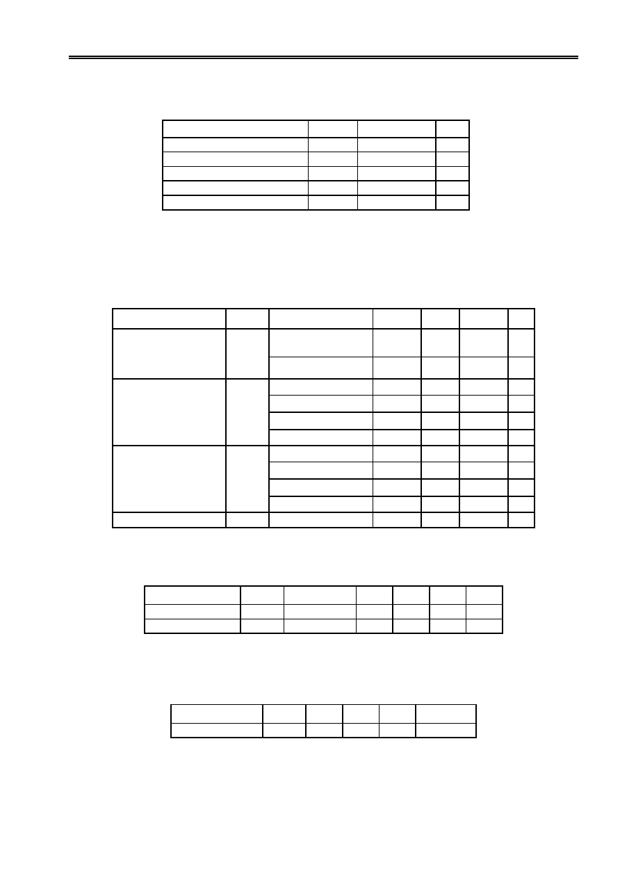
2. Write (PROGRAM ,WRAL, ERAL)
The write instructions (PROGRAM,WRAL,ERAL) automatically begins writing to the non-volatile memory when CS goes
high at the completion of the specified clock input.
The write operation is completed in 10 ms (t
PR
Max.), and the typical write period is less than 5 ms. In the S-29X94A
Series, it is easy to VERIFY the completion of the write operation in order to minimize the write cycle by setting CS to low
and checking the DO pin, which is low during the write operation and high after its completion. This VERIFY procedure
can be executed over and over again.
There are two methods to detect a change in the DO output. One is to detect a change from low to high setting CS to low,
and the other is to detect a change from low to high as a result of repetitous operations of returning the CS to high after
setting CS to low and checking the DO output.
Because all SK and DI inputs are ignored during the write operation, any input of instruction will also be disregarded.
When DO outputs high after completion of the write operation or if it is in the high-impedence state (Hi-Z), the input of
instructions is available. Even if the DO pin remains high, it will enter the high-impedence state upon the recognition of
a high of DI (start-bit) attached to the rising edge of an SK pulse.
DI input should be low during the VERIFY procedure.
2.1 PROGRAM
This instruction writes 16-bit data to a specified address.
After changing CS to low, input a start-bit, op-code (PROGRAM), address, and 16-bit data. If there is a data overflow of
more than 16 bits, only the last 16-bits of the data is considered valid. Changing CS to high will start the PROGRAM
operation. It is not necessary to make the data "1" before initiating the PROGRAM operation.
FIgure 6 WRITE Timing (S-29394A)
t
C D S
X
1 1
3 2
t
P R
b u s y
re a d y
D 1 5
H i-Z
t
S V
1 6
H i-Z
1 7
1 0
9
8
7
6
5
3
2
1
S K
D I
D O
A 0
D 0
4
t
H Z 1
0
A 5
A 6 *
A 7 *
X
0
X
X
1
re a d y
C S
V E R IF Y
* On the S-29194A, A
7
and A
6
are optional.
On the S-29294A, A
7
is optional.

CMOS SERIAL E
2
PROM
S-29X94A Series
8
Seiko Instruments Inc.
2.2 Write all (WRAL)
This instruction writes the same 16-bit data into every address.
After changing CS to low, input a start-bit, op-code (WRAL), address (optional), and 16-bit data. If there is a data
overflow of more than 16 bits, the write data is shifted for every clock in succession and only the last 16-bit data is valid.
Changing CS to high starts the WRAL operation. It is not necessary to make the data "1" before initiating the WRAL
operation.
Figure 7
WRAL Timing
2.3 Erase all (ERAL)
This instruction erases the data in every address. All data changes to "1".
After changing CS to low, input a start-bit, op-code (ERAL), and address (optional) . It is not necessary to input data.
Changing CS to high starts the ERAL operation.
Figure 8 ERAL Timing
3. Write enable (PEN) and Write disable (PDS)
The PEN instruction puts the S-29X94A Series into write enable mode, which accepts PROGRAM, WRAL, and ERAL
instruction. The PDS instruction puts the S-29X94A Series into write disable mode, which refuses PROGRAM, WRAL,
and ERAL instruction.
The S-29X94A Series powers on in write disable mode, which protects data against unexpected, erroneous write
operations caused by noise and/or CPU malfunctions. It should be kept in write disable mode except when performing
write operations.
Figure 9 PEN/PDS Timing
11
=
PEN
00
=
PDS
0
0
X
1
2
3
4
5
6
7
8
DI
CS
SK
X
X
16
X
Hi-Z
17
16
t
PR
1
t
SV
15
14
D15
0
0
8
7
6
5
4
3
2
1
SK
DI
DO
0
D0
Hi-Z
t
HZ1
ready
busy
9
32
X
X
X
X
X
X
X
t
CDS
VERIFY
CS
Standby
Hi-Z
16
t
PR
1
t
SV
15
14
X
0
0
8
7
6
5
4
3
2
1
SK
DI
DO
0
X
Hi-Z
t
HZ1
ready
busy
9
X
X
X
X
X
t
CDS
VERIFY
Standby
CS

CMOS SERIAL E
2
PROM
S-29X94A Series
Seiko Instruments Inc.
9
Receiving a Start-Bit
Three-Wire Interface (DI-DO direct connection)
∑
Please refer Application Note "S-29 & S-93C series EEPROMs Tips, Tricks & Traps" for equivalent circuit of each pin.
A start-bit can be recognized by latching the high level of DI at the rising edge of SK after changing CS to low (Start-Bit
Recognition). The write operation begins by inputting the write instruction and setting CS to high. The DO pin then
outputs low during the write operation and high at its completion by setting CS to low (Verify Operation). Therefore, only
after a write operation, in order to accept the next command by having CS go low, the DO pin is switched from a state of
high-impedence to a state of data output; but if it recognizes a start-bit, the DO pin returns to a state of high-impedence
(see Figure 3).
Make sure that data output from the CPU does not interfere with the data output from the serial memory IC when you
configure a 3-wire interface by connecting DI input pin and DO output pin. Such interference may cause a start-bit fetch
problem.
Although the normal configuration of a serial interface is a 4-wire interface to CS, SK, DI, and DO, a 3-wire interface is
also a possibility by connecting DI and DO. However, since there is a possibility that the DO output from the serial
memory IC will interfere with the data output from the CPU with a 3-wire interface, install a resistor between DI and DO
in order to give preference to data output from the CPU to DI(See Figure 10).
DI
SIO
Figure 10 3-wire interface
DO
CPU
S-29X94A
R : 10~100 k
CMOS SERIAL E
2
PROM
S-29X94A Series
10
Seiko Instruments Inc.
Connecting to the CPU with Serial Port
Memory
Protection
Precaution
Do not apply an electrostatic discharge to this IC that exceeds the performance ratings of the built-in electrostatic
protection circuit.
Figure 11
Connecting Example
Figure 12
Serial Shift Timing
S-29X94A
SO
DI
I/O
SK
SI
CPU
SK
DO
CS
DO
7
DO
6
DO
5
DO
4
DO
3
DO
2
DO
1
DO
0
DI
7
DI
6
DI
5
DI
4
DI
3
DI
2
DI
1
DI
0
SK
SI
SO
CPU data output
CPU data fetch
Figure 13 PROTECT Terminal Input Signal Timing
The S-29X94A Series is capable of protecting the memory. So, the contents of the memory will not be miswritten
due to error run or malfunction of the CPU. When the PROTECT terminal is connected to GND or OPEN, write to
Bank 1 in the memory array is prohibited (50
%
of the memory can be protected starting from address 00).
Because the pull-down resistance is connected to the PROTECT terminal internally, the memory can be
automatically protected when the PROTECT terminal is OPEN. When the protection is valid, the data in the
memory of Bank 1 will not be rewritten. However, because the write control circuit inside the IC functions, the next
instruction cannot be executed during the time period of writing (t
PR
). While write instruction is being input and
write is being executed, always connect the PROTECT terminal to "H", "L" or OPEN, and leave the input signal
unchanged (see Figure 13).
CS
VERIFY
Write Instruction Input
DO
busy
Hi-Z
Hi-Z
ready
t
PR
0.2
Ķ
s Min.
0.2
Ķ
s Min.
PROTECT
DI
SK
CMOS SERIAL E
2
PROM
S-29X94A Series
Seiko Instruments Inc.
11
Characteristics
1. DC Characteristics
Ta (įC)
0.4
0.2
V
CC
=
5.5 V
f
SK
=
2 MHz
DATA
=
0101
0
-
40
0
85
I
CC1
(mA)
Ta (įC)
0.4
0.2
V
CC
=
3.3 V
f
SK
=
500 KHz
DATA
=
0101
0
-
40
0
85
I
CC1
(mA)
Ta (įC)
0.4
0.2
V
CC
=
1.8 V
f
SK
=
10 KHz
DATA
=
0101
0
-
40
0
85
I
CC1
(mA)
0.4
0.2
0
2 3 4
5 6
7
Ta
=
25 įC
f
SK
=
1 MHz, 500 KHz
DATA
=
0101
V
CC
(V)
0.4
0.2
0
2
3
4
5 6
7
Ta
=
25 įC
f
SK
=
100 KHz, 10 KHz
DATA
=
0101
V
CC
(V)
0.4
0.2
0
I
CC1
(mA)
V
CC
=
5.0 V
Ta
=
25 įC
1M 2M
10K 100K
f
SK
(Hz)
Ta (įC)
1.0
0.5
V
CC
=
5.5 V
0
-
40
0
85
I
CC2
(mA)
Ta (
įC)
1.0
0.5
V
CC
=
3.3 V
0
-
40
0
85
I
CC2
(mA)
I
CC1
(mA)
I
CC1
(mA)
100 KH
Z
~
10 KH
Z
~
1MHZ
~
~
500 KH
Z
1.1 Current consumption (READ) I
CC1
--
Ambient temperature Ta
1.2 Current consumption (READ) I
CC1
--
Ambient temperature Ta
1.3 Current consumption (READ) I
CC1
--
Ambient temperature Ta
1.4 Current consumption (READ) I
CC1
--
Power supply voltage V
CC
1.5 Current consumption (READ) I
CC1
--
Power supply voltage V
CC
1.6 Current consumption (READ) I
CC1
≠
Clock frequency f
SK
1.7 Current consumption (PROGRAM) I
CC2
-
Ambient temperature Ta
1.8 Current consumption (PROGRAM) I
CC2
-
Ambient temperature Ta
CMOS SERIAL E
2
PROM
S-29X94A Series
12
Seiko Instruments Inc.
Ta (įC)
1.0
0.5
V
CC
=
5.5 V
DO
=
0 V
0
-
40
0
85
I
LO
(
Ķ
A)
Ta (įC)
1.0
0.5
V
CC
=
5.5 V
DO
=
5.5 V
0
-
40
0
85
I
LO
(
Ķ
A)
1.0
0.5
0
2
3
4
5
6
7
Ta
=
25 įC
V
CC
(V)
I
CC2
(mA)
10
-6
10
-7
10
-8
10
-9
10
-10
V
CC
=
5.5 V
10
-11
Ta (įC)
-
40
0
85
Ta (įC)
1.0
0.5
V
CC
=
5.5 V
CS, SK, DI,
TEST
=
0 V
0
-
40
0
85
I
LI
(
Ķ
A)
Ta (įC)
1.0
0.5
0
-
40
0
85
V
CC
=
5.5 V
CS, SK, DI,
TEST
=
5.5 V
I
SB
(A)
I
LI
(
Ķ
A)
Ta (įC)
4.6
4.4
V
CC
=
4.5 V
I
OH
=-
400
Ķ
A
-
40
0
85
V
OH
(V)
4.2
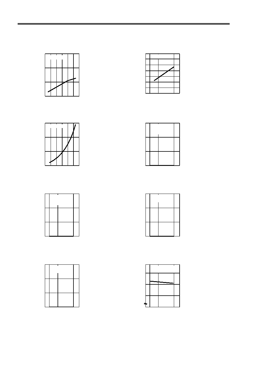
1.9 Current consumption (PROGRAM) I
CC2
-
Power supply voltage V
CC
1.10 Standby current consumption I
SB
--
Ambient temperature Ta
1.14 Output leakage current I
LO
-
Ambient temperature Ta
1.15 Output leakage current I
LO
-
Ambient temperature Ta
1.16 High level output voltage V
OH
-
Ambient temperature Ta
1.12 Input leakage current I
LI
-
Ambient temperature Ta
1.13 Input leakage current I
LI
-
Ambient temperature Ta
40
20
0
2
3
4
5
6
7
Ta
=
25 įC
V
CC
(V)
I
PD
(
Ķ
A)
1.11 Pull-Down current I
PD
-
Power supply voltage V
CC
CMOS SERIAL E
2
PROM
S-29X94A Series
Seiko Instruments Inc.
13
Ta (įC)
2.5
2.4
V
CC
=
2.5 V
I
OH
=-
100
Ķ
A
-
40
0
85
V
OH
(V)
2.3
Ta (įC)
0.3
0.2
V
CC
=
4.5 V
I
OL
=
2.1 mA
-
40
0
85
V
OL
(V)
0.1
Ta (įC)
0.03
0.02
V
CC
=
1.8 V
I
OL
=
100
Ķ
A
-
40
0
85
V
OL
(V)
0.01
Ta (įC)
-
10.0
-
5.0
V
CC
=
4.5 V
V
OH
=
2.4 V
0
-
40
0
85
I
OH
(mA)
Ta (įC)
-
4
-
2
V
CC
=
2.7 V
V
OH
=
2.0 V
0
-
40
0
85
I
OH
(mA)
Ta (
įC)
-
4
-
2
V
CC
=
2.5 V
V
OH
=
1.8 V
0
-
40
0
85
I
OH
(mA)
Ta (įC)
20
10
V
CC
=
4.5 V
V
OL
=
0.45 V
0
-
40
0
85
I
OL
(mA)
1.18 High level output voltage V
OH
-
Ambient temperature Ta
1.19 Low level output voltage V
OL
-
Ambient temperature Ta
1.20 Low level output voltage V
OL
-
Ambient temperature Ta
1.21 High level output current I
OH
-
Ambient temperature Ta
1.22 High level output current I
OH
-
Ambient temperature Ta
1.23 High level output current I
OH
-
Ambient temperature Ta
1.24 Low level output current I
OL
-
Ambient temperature Ta
Ta (įC)
2.7
2.6
V
CC
=
2.7 V
I
OH
=-
100
Ķ
A
-
40
0
85
V
OH
(V)
2.5
1.17 High level output voltage V
OH
-
Ambient temperature Ta
CMOS SERIAL E
2
PROM
S-29X94A Series
14
Seiko Instruments Inc.
Ta (įC)
3.0
2.0
0
-
40
0
85
3.0
1.5
0
1 2 3
4 5
6
Ta
=
25 įC
CS, SK, DI,
PROT
V
CC
(V)
V
INV
(V)
7
V
INV
(V)
V
CC
=
5.0 V
CS, SK, DI
PROT
1.27 Input inversion voltage V
INV
-
Ambient temperature Ta
1.26 Input inversion voltage V
INV
-
Power supply voltage V
CC
Ta (įC)
1.0
0.5
V
CC
=
1.8 V
V
OL
=
0.1 V
0
-
40
0
85
I
OL
(mA)
1.25 Low level output current I
OL
-
Ambient temperature Ta

CMOS SERIAL E
2
PROM
S-29X94A Series
Seiko Instruments Inc.
15
2. AC Characteristics
10 K
2
3
4
5
Ta
=
25 įC
V
CC
(V)
f
max
(Hz)
1
4
2
2 3 4
5 6
7
Ta
=
25 įC
V
CC
(V)
t
PR
(ms)
1
100 K
1 M
2 M
Ta (įC)
6
4
V
CC
=
5.0 V
-
40
0
85
2
t
PR
(ms)
Ta (įC)
6
4
V
CC
=
3.0 V
-
40
0
85
2
t
PR
(ms)
Ta (įC)
0.6
0.4
V
CC
=
2.7 V
-
40
0
85
0.2
t
PD
(
Ķ
s)
Ta (įC)
0.3
0.2
V
CC
=
4.5 V
-
40
0
85
0.1
t
PD
(
Ķ
s)
Ta (įC)
0.6
0.4
V
CC
=
1.8 V
-
40
0
85
0.2
t
PD
(
Ķ
s)
2.7 Data output delay time t
PD
-
Ambient temperature Ta
2.6 Data output delay time t
PD
-
Ambient temperature Ta
2.5 Data output delay time t
PD
-
Ambient temperature Ta
2.3 Program time t
PR
-
Ambient temperature Ta
2.4 Program time t
PR
-
Ambient temperature Ta
2.1 Maximum operating frequency f
max
-
Power supply voltage V
CC
2.2 Program time t
PR
-
Power supply voltage V
CC

CMOS SERIAL E
2
PROM
S-29X94A Series
16
Seiko Instruments Inc.
Ordering Information
1. 8-pin DIP
2.
8-pin SOP
S-29194AFJA
S-29294AFJA
S-29394AFJA
S-29X94A
XX X
Package type
A
Package DP:
DIP
FJ
:
SOP1
Product name
S-29194A : 1K-bit
S-29294A
:
2K-bit
S-29394A
:
4K-bit
See Pin Assignment, (Figure 1)
S-29194ADPA
S-29294ADPA
S-29394ADPA

DP008-A
011129
1
4
8
5
0.5Ī0.1
2.54
1.0
1.5
0į~15į
0.3
+0.1
-0.05
7.62
9.3(9.6max)
No.:DP008-A-P-SD-1.0
n 8-Pin DIP
Unit:mm
lDimensions
l Reel Specifications
l Tape Specifications
l Dimensions
n 8-pin SOP
Unit : mm
Ý2.0Ī0.05
Ý1.55Ī0.05
4.0Ī0.1(10-pitches : total 40.0Ī0.2)
0.3Ī0.05
2.1Ī0.1
8.0Ī0.1
5įmax.
6.7Ī0.1
2.0Ī0.05
0.4Ī0.05
1.27
1
4
8
5
5.02Ī0.2
0.20Ī0.05
5
8
1
4
TB
Feed direction
2Ī0.5
13.5Ī0.5
60į
2Ī0.5
Ý13Ī0.2
Ý21Ī0.8
Winding core
2000 pcs./reel
FJ008-D
Rev.4.0
011113

∑
The information described herein is subject to change without notice.
∑
Seiko Instruments Inc. is not responsible for any problems caused by circuits or diagrams described herein
whose related industrial properties, patents, or other rights belong to third parties. The application circuit
examples explain typical applications of the products, and do not guarantee the success of any specific
mass-production design.
∑
When the products described herein are regulated products subject to the Wassenaar Arrangement or other
agreements, they may not be exported without authorization from the appropriate governmental authority.
∑
Use of the information described herein for other purposes and/or reproduction or copying without the
express permission of Seiko Instruments Inc. is strictly prohibited.
∑
The products described herein cannot be used as part of any device or equipment affecting the human
body, such as exercise equipment, medical equipment, security systems, gas equipment, or any apparatus
installed in airplanes and other vehicles, without prior written permission of Seiko Instruments Inc.
∑
Although Seiko Instruments Inc. exerts the greatest possible effort to ensure high quality and reliability, the
failure or malfunction of semiconductor products may occur. The user of these products should therefore
give thorough consideration to safety design, including redundancy, fire-prevention measures, and
malfunction prevention, to prevent any accidents, fires, or community damage that may ensue.