Document Outline
- S-3510 Series
- Cover
- Features
- Applications
- Package
- Block Diagram
- Pin Assignment
- Pin Function
- Command Configuration
- Data Configuration
- Ordering Information
- Absolute Maximum Ratings
- Recommended Operating Conditions
- Oscillation Characteristics
- DC Characteristics
- AC Characteristics 1
- AC Characteristics 2
- AC Characteristics 3
- Timing Charts
- Operation
- Application Circuit Examples
- Characteristics
- Package Drawing

Rev. 1.2
_00
REAL-TIME CLOCK
S-3510 Series
Seiko Instruments Inc.
1
The S-3510 is a series of CMOS real-time clock ICs that inputs/
outputs serial clock or calendar data into/from the CPU.
Features
∑ Operating power supply:
1.7 V to 5.5 V
∑ Low current consumption: 1.2 ĶA typ. at 3.0 V
(S-3510AFFJA:
2.0
ĶA typ. at 3.0 V)
∑ BCD output of second, minute, hour, day, date, month and year
∑ Easy serial interface to CPU with 3 lines (SIO, SCK, and CS)
∑ Built-in automatic calendar, automatic leap-year calculation up to 2099.
∑ Built-in voltage detector
∑ Built-in constant voltage circuit
∑ Built-in 32 kHz oscillation circuit (Built-in Cg/Cd, or Cd only)
I Applications
∑ Video cameras
∑ FAXes
∑ Cellular phones
∑ Printers
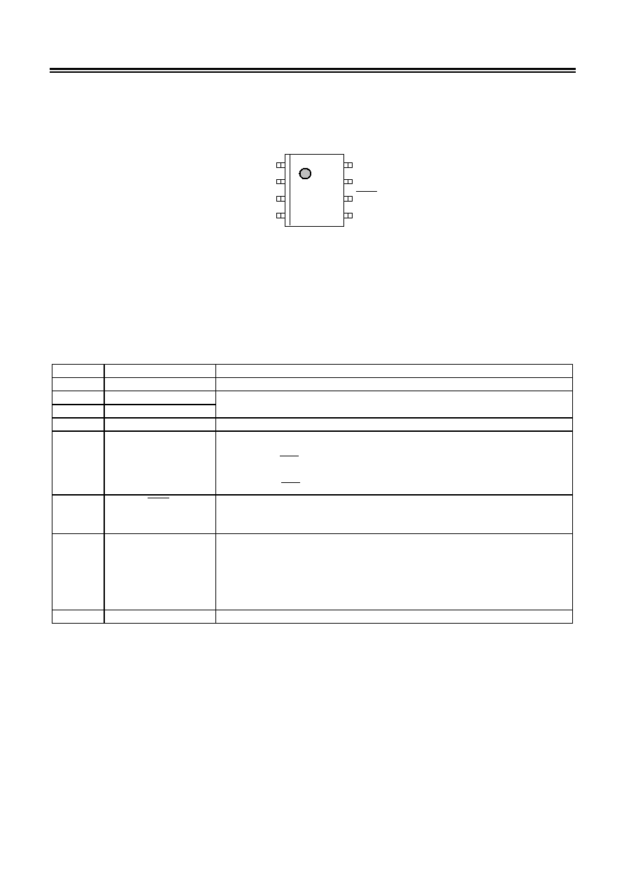
I Package
∑ 8-Pin SOP (Pin pitch : 1.27 mm) (Package drawing code: FJ008-D)

REAL-TIME CLOCK
S-3510 Series
Rev. 1.2
_00
2
Seiko Instruments Inc.
I Block Diagram
Figure 1
SIO
Sec.
Min.
Hr.
Day
Date
Mon.
Year
Counter
Sec.
Min.
Hr.
Day
Date Mon.
Year
Shift Register
Status Register
Serial Interface
&
Controller
SCK
CS
OSC
&
Divider
XIN
XOUT
TPOUT
Voltage
Detector
VDD
VSS
REAL-TIME CLOCK
Rev. 1.2
_00
S-3510 Series
Seiko Instruments Inc.
3
I Pin Assignment
Figure 2
I Pin Function
Table 1
No. Name
Function
1
TPOUT
Standard signal output (Nch open-drain output or CMOS output)
2 XOUT
3 XIN
Connects to the X'ftal resonator (f
=32,768 Hz)
Built-in Cg/Cd, or Cd only
4
VSS
Power supply (GND)
5
CS
Chip select input (Built-in pull-down resistance) :
"H": The SIO pin is capable of inputting/outputting data.
The SCK pin is capable of accepting the input.
"L": The SIO pin is at Hi-Z.
The SCK pin is not capable of accepting the input.
6 SCK
Clock
input
:
Inputs and outputs data from the SIO pin in synchronization with the
clock. The clock cannot be accepted when the CS pin is "L".
7
SIO
Serial data input/output :
When the CS is "L", the SIO pin is at "Hi-Z". When the CS pin changes
from "L" to "H", it serves as the input pin. The SIO pin is assigned to the
input or output pin according to the next command data. The type of
output is either Nch open-drain or CMOS depending upon the model of
the IC you use.
8
VDD
Positive power supply
8
7
6
5
1
2
3
4
TPOUT
XOUT
XIN
VSS
8-Pin SOP
Top view
VDD
SIO
SCK
CS
REAL-TIME CLOCK
S-3510 Series
Rev. 1.2
_00
4
Seiko Instruments Inc.
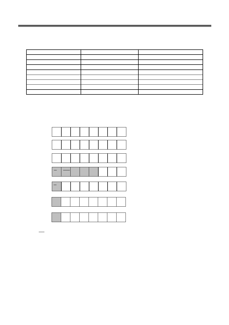
I Command Configuration
Table 2
Command Code
Note
READ 1(Data Read)
1 1 1 0
◊ ◊ ◊ ◊
Output from the year data
READ 2(Data Read)
1 1 1 1
◊ ◊ ◊ ◊
Output from the day data
WRITE 1(Data Write)
1 0 0 1
◊ ◊ ◊ ◊
Input from the year data
WRITE 2(Data Write)
1 0 0 0
◊ ◊ ◊ ◊
Input from the day data
STATUS WRITE
1 0 1 1 D3 D2 D1 D0
Status write
RESET
1 0 1 0 1 0 1 0
Initialization
TEST START
1 1 0 1 0 1 0 1
Test mode start
TEST END
1 1 0 1 1 0 1 0
Test mode end
I Data Configuration
The S-3510 series is provided with a timer data BCD (Binary Coded Decimal) display
*1
device and an
automatic calendar. A set of flags are configured as follows:
*1.
AM/PM Flag :
When writing in 12-hour display mode, always input 0 for AM and 1 for PM.
In 24-hour display mode, it is unnecessary as both 1 and 0 are ignorged.
However, when reading the time in either display mode 0 is read as AM 1 as PM.
BLD Flag :
When a decrease in the voltage is detected, it is set to 1. This is valid during
reading and is invalid during writing.
POW Flag :
1 is set at the power on, and cleared through the RESET command.
This flag is ingored during writing.
TEST Flag
When the test mode is set, it is set to 1. When the bit is 1, always use the TEST
END or RESET command to set to 0. This bit is valid for reading and ignored
during writing.
Hour data (0 to 23 or 0 to 11) and flags
12/24
Y4
Y5
Y6
Y7
0
0
0
M0
M1
M2
M3
M4
POW
S0
S1
S2
S3
S4
S5
S6
BLD
H0
H1
H2
H3
H4
H5
0
AM/PM
TPF FRE
TPEN
Y3
Y2
Y1
Y0
0
0
D5
D4
D3
D2
D1
D0
W2
W1
W0
m6
m5
m4
m3
m2
m1
m0
Year data (0 to
99)
Month data (1 to 12)
Date data (1 to 31)
Status and day data (1 to 7)
Minute data (0 to 59) and flags
Second data (0 to 59) and
flags
TEST

REAL-TIME CLOCK
Rev. 1.2
_00
S-3510 Series
Seiko Instruments Inc.
5
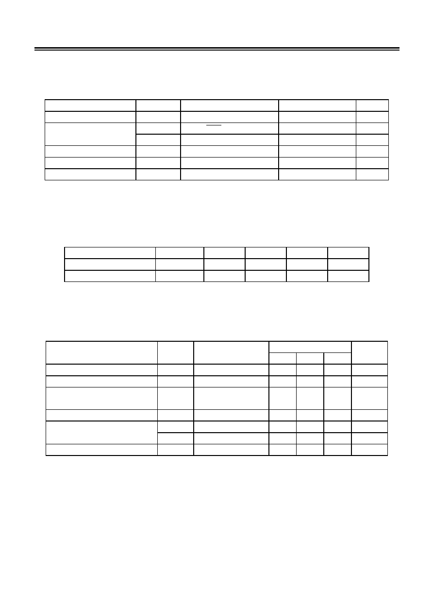
I Ordering Information
Table 3
Model No.
SIO output
TPOUT output
TPOUT
output form
Oscillation
circuit capacity
S-3510ANFJA
Nch open-drain
Selection of 1 H
Z
/
32,768 H
Z
by command
Nch open-drain
Internal Cg, Cd
S-3510ACFJA
CMOS
Selection of 1 H
Z
/
32,768 H
Z
by command
Nch open-drain
Internal Cg, Cd
S-3510ADFJ CMOS
32,768
H
Z
Nch open-drain
External Cg,
Internal Cd
S-3510AEFJ
Nch open-drain
32,768 H
Z
Nch open-drain
Internal Cg, Cd
S-3510AFFJ CMOS
32,768
H
Z
CMOS External
Cg,
Internal Cd
REAL-TIME CLOCK
S-3510 Series
Rev. 1.2
_00
6
Seiko Instruments Inc.
I Absolute Maximum Ratings
Table 4
(Unless otherwise specified : Ta
=25įC)
Parameter Symbol Conditions
Ratings Unit
Power supply voltage
V
DD
-
V
SS
-0.3 to V
SS
+7.0 V
V
IN1
SCK, CS, SIO
V
SS
-0.3 to V
SS
+7.0 V
Input Voltage
V
IN2
SIO (CMOS output)
V
SS
-0.3 to V
DD
+0.3 V
Output voltage
V
OUT
TPOUT, SIO
V
SS
-0.3 to V
SS
+7.0 V
Operating temperature
T
opr
V
DD
=3.0 V
-30 to +80
įC
Storage temperature
T
stg
-
-55 to +125
įC
Caution The absolute maximum ratings are rated values exceeding which the product could suffer
physical damage. These values must therefore not be exceeded under any conditions.
Recommended
Operating
Conditions
Table 5
Parameter Symbol
Min.
Typ.
Max.
Unit
Power supply voltage
V
DD
1.7 3.0 5.5 V
Operating temperature
T
opr
-20
-
+70
įC
I Oscillation Characteristics
Table 6
(Unless otherwise specified : Ta
=25įC, V
DD
=3.0 V, X'ftal resonator: SII Quartz Techno Ltd., DS-VT-200 (R
1
=30 k, C
L
*1
=6 pF, 32,768 Hz))
Standard
Parameter Symbol
Conditions
Min. Typ. Max.
Unit
Oscillation start voltage
V
STA
Within 10 s
1.7
- 5.5 V
Oscillation start time
T
STA
-
-
- 3.0 s
Frequency deviation between
ICs
IC
-
-10
-
+10 ppm
Frequency voltage deviation
V V
DD
=1.7 V to 5.5 V
-3
-
+3 ppm/V
C
IN1
*2
Applied to X
IN
- 12 - pF
Input capacitance
C
IN2
*3
Applied to X
IN
- 8 - pF
Output capacitance
C
OUT
*4
Applied to X
OUT
- 12 - pF
*1. The load capacitance (C
L
) changes depending upon the capacitance of the PCB mounted onto the IC.
Adjust the load capacitance.
*2 Applied to S-3510ANFJx, S-3510ACFJx, S-3510AEFJA (Internal)
*3 Applied to S-3510ADFJA, S-3510AFFJA (External)
*4 Applied to S-3510ANFJx, S-3510ACFJx, S-3510AEFJA, S-3510ADFJA, S-3510AFFJA (Internal)
REAL-TIME CLOCK
Rev. 1.2
_00
S-3510 Series
Seiko Instruments Inc.
7
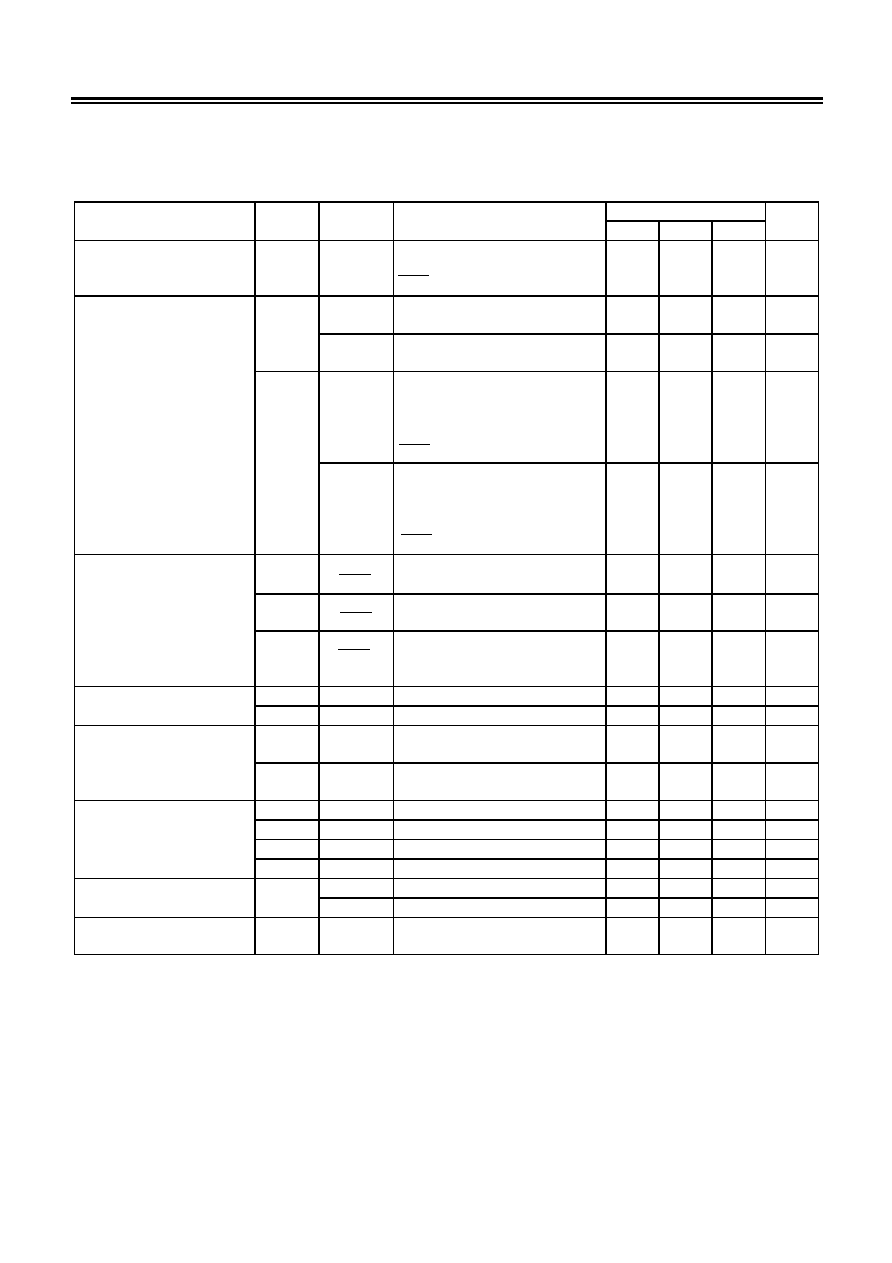
I DC Characteristics
Table 7
Unless otherwise specified:
Ta
=25 įC,V
DD
=3.0 V, X'tal resonator:SII Quartz Techno Ltd.,
DS-VT-200 (R
1
=30 k, C
L
=6 pF, 32,768 Hz)
Standard
Parameter Symbol
Applicable
pin
Conditions
Min. Typ. Max.
Unit
Operating voltage range
V
DD
- Ta=-20įC to +70įC,
Communications when
SCK
=100 kHz
1.7 3.0 5.5 V
- CS=0 V. No output load.
Communication inhibit
*1
-
1.2 2.0
ĶA
I
DD1
- CS=0 V. No output load.
Communication inhibit
*2
-
2.0 3.5
ĶA
-
The current which flows
through the CS is not
included. No output load.
Communications when
SCK
=100 kHz
*3
-
10 30
ĶA
Power current
consumption
I
DD2
-
The current which flows
through the CS is not
included. No output load.
Communications when
SCK
=100 kHz
*4
-
30 60
ĶA
I
IHL1
SIO,
SCK
V
IN
=5.5 V
*5
-0.5
-
0.5
ĶA
I
IHL2
SIO,
SCK
V
IN
=V
DD
*6
-0.5
-
0.5
ĶA
Input leak current
I
ILL
SIO,
SCK,
CS
V
IN
=0 V
-0.5
-
0.5
ĶA
I
IH2
CS
V
IN
=5.5 V
-
10 30
ĶA
Input current
I
IH3
CS
V
IN
=0.4 V
30 100 300
ĶA
V
IH
-
-
0.8
◊V
DD
-
-
V
Input voltage
V
IL
-
-
-
-
0.2
◊V
DD
V
I
OL1
TPOUT
V
IN
=0.4 V
200
-
-
ĶA
I
OL2
SIO
V
IN
=0.4 V
500
-
-
ĶA
I
OH1
TPOUT
V
IN
=2.6 V
*7
-
-
-200
ĶA
Output current
I
OH2
SIO
V
IN
=2.6 V
*8
-
-
-500
ĶA
- Ta=25įC
1.8 2.0 2.2 V
Voltage detection
voltage
V
DET
- Ta=-20įC to +70įC
1.72
-
2.3 V
BLD current
consumption
I
BLD
- Ta=-20įC to +70įC
-
0.3 1.0
ĶA
*1. Applied to the products except S-3510AFFJA
*2. Applied to S-3510AFFJA
*3. Applied to 3510ANFJx, S-3510ADFJA, S-3510AFFJA
*4. Applied to S-3510ACFJx, S-3510ADFJA, S-3510AFFJA
*5. Applied to S-3510ANJFx, S-3510AEFJA
*6. Applied to S-3510ACFJx, S-3510ADFJA, S-3510AFFJA
*7. Applied to S-3510AFFJA
*8. Applied to S-3510ACFJx, S-3510ADFJA, S-3510AFFJA

REAL-TIME CLOCK
S-3510 Series
Rev. 1.2
_00
8
Seiko Instruments Inc.
I AC Characteristics 1
(S-3510ANFJx, S-3510AEFJA, R
L1
=30 k, C
L1
=50 pF)
Conditions: V
DD
=1.7 V to 5.5 V, Ta=-20įC to 70įC, Interface voltage Vcc=5.0 V
Input: V
IH
=0.8◊V
DD
, V
IL
=0.2◊V
DD
, Output: V
OH
=0.8◊V
CC
, V
OL
=0.2◊V
CC
Table 8
Parameter Symbol
Min.
Typ.
Max.
Unit
Clock pulse width
t
SCK
5
-
250000
Ķs
Setup time prior to the rising of the CS
t
DS
1
-
-
Ķs
Hold time after the rising of the CS
t
CSH
1
-
-
Ķs
Input data setup time
t
ISU
1
-
-
Ķs
Input data hold time
t
IHO
1
-
-
Ķs
Output data determination time
t
ACC
-
-
3.5
Ķs
Setup time prior to the falling of the CS
t
CSS
1
-
-
Ķs
Hold time after the falling of the CS
t
DH
1
-
-
Ķs
Input rising/falling time
t
R
, t
F
-
-
0.1
Ķs
I AC Characteristics 2
(S-3510ACFJx, S-3510ADFJA, S-3510AFFJA, C
L1
=50 pF)
Conditions : V
DD
=5.0Ī0.5 V, Ta=-20įC to 70įC
Input: V
IH
=0.8◊V
DD
, V
IL
=0.2◊V
DD
, Output: V
OH
=0.8◊V
DD
, V
OL
=0.2◊V
DD
Table 9
Parameter Symbol
Min.
Typ.
Max.
Unit
Clock pulse width
t
SCK
0.5
-
250000
Ķs
Setup time prior to the rising of the CS
t
DS
0.1
-
-
Ķs
Hold time after the rising of the CS
t
CSH
0.1
-
-
Ķs
Input data setup time
t
ISU
0.1
-
-
Ķs
Input data hold time
t
IHO
0.1
-
-
Ķs
Output data determination time
t
ACC
-
-
0.3
Ķs
Setup time prior to the falling of the CS
t
CSS
0.1
-
-
Ķs
Hold time after the falling of the CS
t
DH
0.1
-
-
Ķs
Input rising/falling time
t
R
, t
F
-
-
0.05
Ķs
I AC Characteristics 3
(S-3510ACFJx, S-3510ADFJA, S-3510AFFJA, C
L1
=50 pF)
Conditions : V
DD
=3.0Ī0.6 V, Ta=-20įC to 70įC
Input: V
IH
=0.8◊V
DD
, V
IL
=0.2◊V
DD
, Output: V
OH
=0.8◊V
DD
, V
OL
=0.2◊V
DD
Table 10
Parameter Symbol
Min.
Typ.
Max.
Unit
Clock pulse width
t
SCK
1.0
-
250000
Ķs
Setup time prior to the rising of the CS
t
DS
0.2
-
-
Ķs
Hold time after the rising of the CS
t
CSH
0.2
-
-
Ķs
Input data setup time
t
ISU
0.2
-
-
Ķs
Input data hold time
t
IHO
0.2
-
-
Ķs
Output data determination time
t
ACC
-
-
0.6
Ķs
Setup time prior to the falling of the CS
t
CSS
0.2
-
-
Ķs
Hold time after the falling of the CS
t
DH
0.2
-
-
Ķs
Input rising/falling time
t
R
, t
F
-
-
0.05
Ķs

REAL-TIME CLOCK
Rev. 1.2
_00
S-3510 Series
Seiko Instruments Inc.
9
I Timing Charts
t
CSH
t
DS
t
DH
t
DH
t
CSS
t
DS
CS
SCK
SIO
Figure 3
Figure 5
80
%
80
%
20
%
20
%
50
%
20
%
80
%
20
%
20
%
80
%
t
ACC
t
SCK
t
SCK
t
R
,t
F
t
F
t
R
t
ISU
SCK
Input data
t
IHO
50
%
SCK
Output data
Figure 4
REAL-TIME CLOCK
S-3510 Series
Rev. 1.2
_00
10
Seiko Instruments Inc.
I Operation
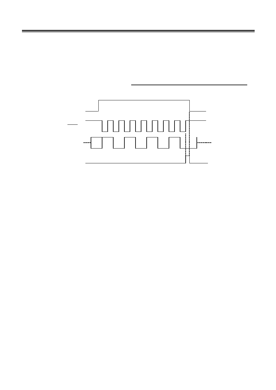
(1) Initialization
When the power is switched on, the POW flag is assigned via the power-on detector. Always turn the CS
to"L". Regardless of the logic of the POW flag, initialization must be executed, therefore always send the
RESET command (10101010) from the CPU.
This allows the divider, counter and status register of the S-3510 series to be reset. Namely, the
second, minute, hour, day, date, month, and year (00 s, 00 min., 00 hr., Sunday (1), January (01), 00 year)
are set, and the counter starts to operate upon the falling edge of the CS.
Figure 6
SIO
CS
SCK
Input
X
1
0
1
0
1
0
1
0
Reset
REAL-TIME CLOCK
Rev. 1.2
_00
S-3510 Series
Seiko Instruments Inc.
11
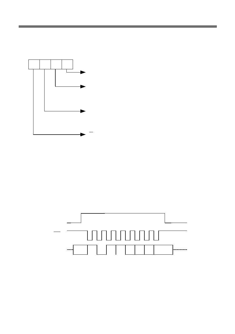
(2) Write to the Status Register
The S-3510 series is provided with a 4-bit status register. To write the data in the register, send the
STATUS WRITE command (1011D3D2D1D0). This data is retrieved in synchronization with the falling edge
of the CS.
*1. When the frequency-select bit is rewritten during operation, the first pulse generated immediately after
the CS is turned to "L" cannot be output at the correct frequency
Upon initialization, (D3, D2, D1, D0) is set to (1, 0, 1, 0). In other words,
(a) In the S-3510ANFJx, the S-3510ACFJA, 1 Hz is output from TPOUT
, and the status is set to the
24-hour display mode.
(b) In the S-3510AEFJx, the S-3510ADFJA, the S-3510AFFJA, 32768 Hz is output from TPOUT
, and
the status is set to the 24-hour display mode.
When initialization is not executed, the data of the status register is not specified. Always execute
initialization when switching on the power.
Figure 7
Free bit: Stores the information according to a user-specified memory
bit. It does not affect the function of the timer. Reset to"0"
during initialization.
TPOUT output frequency-select bit
*1
. In the S-3510ANFJA, the S-3510ACFJx
0: 32768 Hz
1: 1 Hz
In the S-3510AEFJA, the S-3510ADFJA, the S-3510AFFJA
0, 1: 32768 Hz (It can be used as Free bit)
TPOUT enable bit
In the S-3510ANFJx, the S-3510ACFJx
0: Output
1: High impedance
In the S-3510AEFJA, the S-3510ADFJA, the S-3510AFFJA
0, 1: Output (It can be used as Free bit)
12/24-hour display change bit 0: 12-hour display
1: 24-hour display
D3
D2
D1
D0
D1
D2
CS
X
1
0
1
D3
1
D0
SIO
SCK

REAL-TIME CLOCK
S-3510 Series
Rev. 1.2
_00
12
Seiko Instruments Inc.
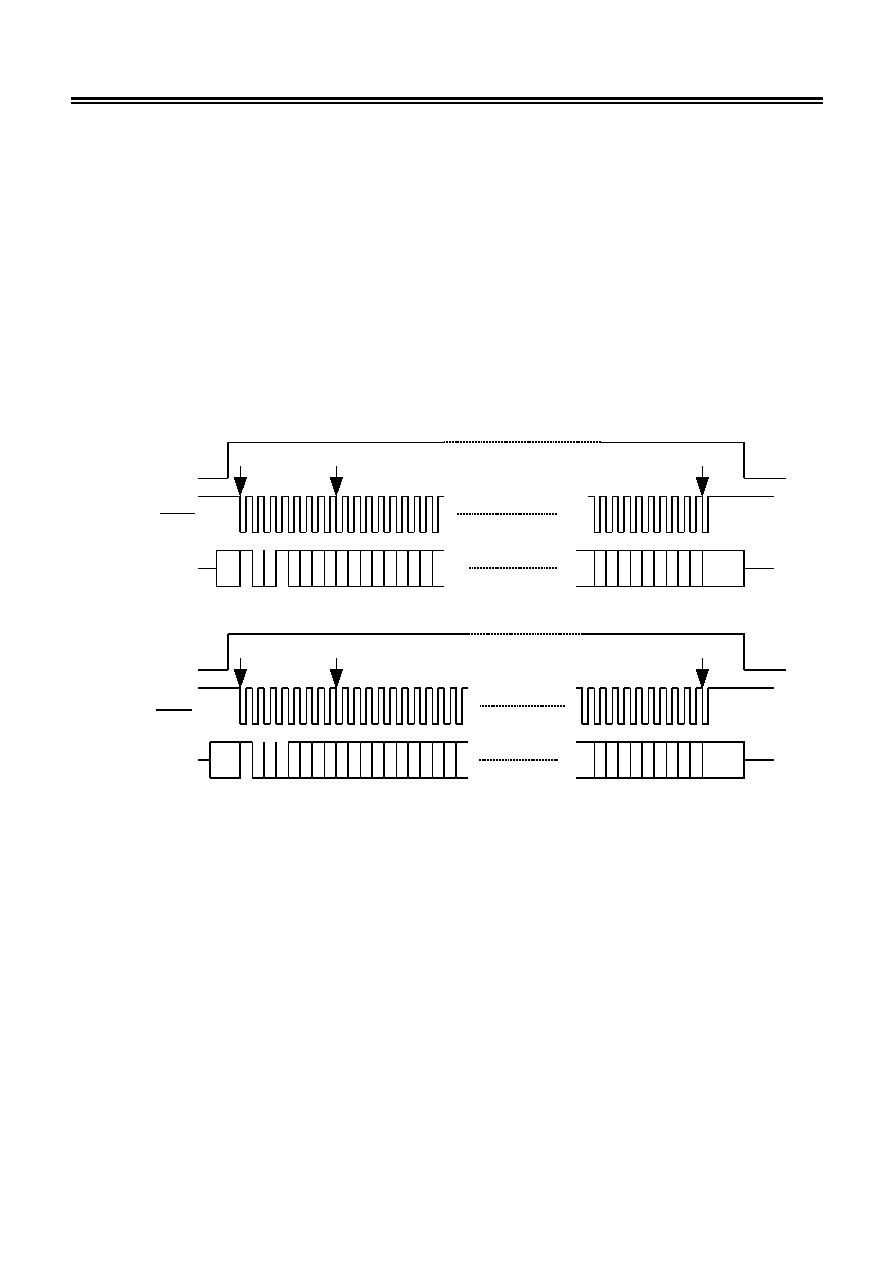
(3) Data Read
The time data can be read by sending the READ command after the CS goes "H". The data is output in
order of the LSB of the day or year.
After the READ command is interpreted, the time data is transmitted from the counter to the shift register.
In synchronization with the falling edge of the 9th clock, the SIO status changes from input to output, and
the LSB of the timer register is output. After then, in synchronization with the falling edge of the clock, the
time data is output from the shift register.
If the power supply voltage detector activates, the MSB (BLD bit) is set to"1", which allows the power
supply voltage to be monitored. For more details, refer to the "(6) Voltage Detector".
Figure 8
WWW
0 1 2
m
6
m
5
12
24
m
6
BLD
T
P
E
N
T
P
F
F
R
E
6
9
1
S S S S S S
1 2 3 4 5 6
S
0
P
O
C
Y
7
Y
6
Y
5
Y
4
Y
3
Y
2
Y
1
Y
0
X
X
X
X
0
1
1
1
X
M
0
Output Mode Change
READ1
mode
CS
SCK
SIO
READ2
mode
4
9
1
S S S S S S
1 2 3 4 5 6
S
0
P
O
C
X
X
X
X
1
1
1
1
X
BLD
H
0
m
5
CS
SCK
SIO
T
e
s
t
Output Mode Change
REAL-TIME CLOCK
Rev. 1.2
_00
S-3510 Series
Seiko Instruments Inc.
13
(4) Data Write
Sending the WRITE command after the CS changes from "L" to"H" halts the update operation and resets
the frequency divider. This allows the time data to be written. The data is input in order of the LSB of the
day or year. The time data transmitted from the SIO is written in the shift register in synchronization with the
rising edge of the clock. After transmission of the minute data has been completed, the currently-stored
data is transmitted to the counter during the period of the transmission of the second data, and the month-
end correction is executed. The second data is transmitted from the shift register to the second counter in
synchronization with the point where the CS changes from "H" to"L". Accordingly, the second data error
processing is not performed. Turning the CS to "L" allows the divider to run and update operation to start.
One second after, the carry-up signal is transmitted to the second counter. If non-existent data is written in
the second counter, the second counter is set to "00", and the carry-up signal is transmitted to the minute
counter.
Caution When the CS is turned to "L", correct data cannot be written. Never turn the CS to "L"
before WRITE is completed. Refer to the timing chart shown below.
Figure 9
CS
SCK
SIO
WRITE 2 mode
CS
SCK
SIO
W W W
0 1 2
S S S S S S
1 2 3 4 5 6
S
0
H H H
0 1 2
S S S S S S
1 2 3 4 5 6
X
m
6 X
m
5
6
9
1
Y
7
Y
6
Y
5
Y
4
Y
3
Y
2
Y
1
Y
0
X
X
X
X
1
0
0
1
X
M
0
WRITE1 mode
X
X
X X X
m
6 X
4
9
1
S
0
X
X
X
0
0
0
1
X
m
5
X

REAL-TIME CLOCK
S-3510 Series
Rev. 1.2
_00
14
Seiko Instruments Inc.
<1> Dividing steps are reset at "H".
<2> All bits of the minute, hour and day (date, month, and year) counter are zero cleared at "H".
<3> With respect to the bit where the data written in the minute, hour and day (date, month, and year)
counter is 1, 1 is set at "H".
<4> Invalid data processing is performed at "H".
<5> Month-end processing is performed at "H".
<6> The second data is written at "H".
Figure 10
X
1
CS
SCK
SIO
<6>
<4>
<3>
<2>
<1>
S
0
m
6
X X X X
8 9
Y
1
Y
0
0
0
1
S S S S S
2 3 4 5 6
S
1
<5>
X
X

REAL-TIME CLOCK
Rev. 1.2
_00
S-3510 Series
Seiko Instruments Inc.
15
(5) Month-End Correction
When the time data is written in the counter, its validity is checked and either invalid data or month-end
processing is performed.
[Data Processing]
Table 11
Normal data
Error data
Result
Year data
00 to 99
XA to XF, AX to FX
00
Month data
01 to 12
00, 13 to 19, XAto XF
01
Day data
1 to 7
0
1
Date data
01 to 31
00, 32 to 39, XA to XF
01
Hour data (24-hour)
*1
(12-hour)
0 to 23
0 to 11
24 to 29, 3X, XA to XF
12 to 19, XA to XF
00
00
Minute data
00 to 59
60 to 79, XA to XF
00
Second data
*2
00 to 59
60 to 79, XA to XF
00
*1.
Invalid data processing for the second data is performed through the carry pulse 1 second after
the completion of writing. The carry pulse is sent to the minute counter.
*2.
Write 0 or 1 into the AM/PM flag using the 12-hour display.
For the 24-hour display, 0 or 1 is neglected when writing into the AM/PM flag. When reading,
however, 0 is read during 0 to 11 o'clock, and 1 is read during 12 to 23 o'clock.
[Month-End Processing]
Non-existent days at the end of the month are automatically processed as the 1st day of the following
month. For example, April 31 is automatically set to May 1. Leap years are allso adjusted.
(6) Voltage Detector
The S-3510 series incorporates a voltage detector that performs sampling once a second for 62.5 ms.
When the supply voltage goes below the detection voltage, the BLD latch-up circuit latches "H", and
stops sampling.
When the CS is turned to "H", the output of the latch-up circuit is transmitted to the shift register only
when the subsequent command is the READ command.
Reading the BLD bit allows the decrease in the voltage to be monitored.
If the CS is turned to "L" after completing the read, sampling restarts. That is, once a decrease in the
voltage is detected, detection is not performed and the status is kept "H" as long as an initialization is not
performed or a READ command is not sent.
Caution The BLD flag can read 1 when the supply voltage increases and the first read is executed.
After that, however, sampling is permitted. Therefore, when the next read is performed after
sampling of the detector, the BLD flag is reset. Refer to the timing charts shown next:

REAL-TIME CLOCK
S-3510 Series
Rev. 1.2
_00
16
Seiko Instruments Inc.
Figure 12
Sampling
pulse
Carry pulse
(0)
1 s
1 s
Halt
Halt
(1)
(1)
(1) (1)
(1) (1) (0)
V
CC
CS
Latch circuit output
BLD flag
[Timing of Sampling Pulse]
1 Hz
V
DET
Sampling
pulse
0.5 s
0.5 s
7.8 ms
Carry-up timing
Latch timing
62.5 ms
31.25 ms
31.25 ms
62.5 ms
Latch pulse
Figure 11
Halt
REAL-TIME CLOCK
Rev. 1.2
_00
S-3510 Series
Seiko Instruments Inc.
17
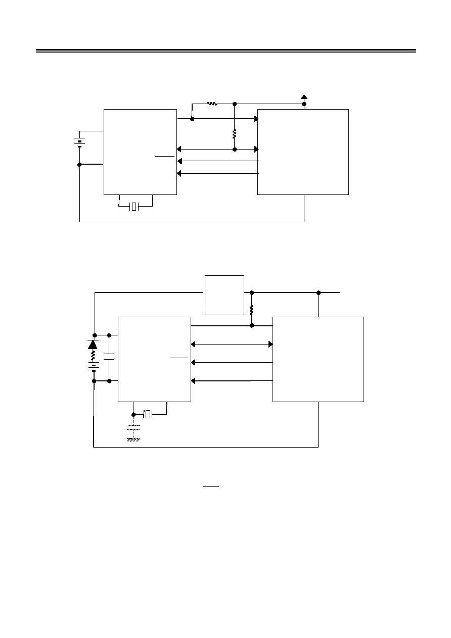
I Application Circuit Examples
(1) S-3510ANFJx, S-3510AEFJx (Nch open-drain output)
Figure 13
(2) S-3510ACFJx, S-3510ADFJx (CMOS output)
Figure 14
Caution In the case of (2) or (3), the voltage of more than V
DD
cannot be
applied to the SIO,CS,SCK. For communication purpose, switch
the system power supply (V
CC
) on, and turn the CS to "H" after the
system power supply stabilizes. Always turn the CS to "L" and
switch the system power supply off.
Vcc
XOUT
XIN
S-3510ANFJx/AEFJA
SCK
SIO
TPOUT
VSS
VDD
CS
VSS
VCC
External CPU
S-3510ACFJx/ADFJA
CS
XOUT
XIN
SCK
SIO
TPOUT
VSS
VDD
VSS
VCC
External CPU
Power
supply
change
circuit

REAL-TIME CLOCK
S-3510 Series
Rev. 1.2
_00
18
Seiko Instruments Inc.
(3) S-3510AFFJ (SIO:CMOS output, TPout:CMOS output)
Figure 15
Caution In the case of (2) or (3), the voltage of more than V
DD
cannot be
applied to the SIO,CS,SCK. For communication purpose, switch
the system power supply (V
CC
) on, and turn the CS to "H" after the
system power supply stabilizes. Always turn the CS to "L" and
switch the system power supply off.
When V
DD
<V
CC
, the SCK and CS terminals can be directly connected to the CPU because there is no flow
of current from the CPU.
I Precautions
∑
The oscillation which uses a quartz crystal resonator is sensitive to external noise which may have an
effect on the accuracy of the watch. Make sure to design your oscillation circuit with this in mind.
A) Configure the quartz crystal resonator as close to the IC as possible.
B) Take measures for sufficient insulation between pins XIN and XOUT.
C) Do not design a circuit where signal lines or the power lines pass close to the oscillation circuit.
∑
When using other resonators, not specified herein or other than the DS-VT-200, always check the accuracy
and stability of the oscillation by changing conditions such as the power supply voltage and temperature on
the actual PCB you use.
∑
The load capacitance (C
L
) of the quartz crystal resonator visibly changes depending upon the capacitance
of the PCB mounted onto the IC. Adjust the load capacitance.
∑
Do not apply an electrostatic discharge to this IC that exceeds the performance ratings of the built-in
electrostatic protection circuit.
∑
SII claims no responsibility for any disputes arising out of or in connection with any infringement by
products including this IC of patents owned by a third party.
S-3510AFFJA
CS
XOUT
XIN
SCK
SIO
TPOUT
VSS
VDD
VSS
VCC
External CPU
REAL-TIME CLOCK
Rev. 1.2
_00
S-3510 Series
Seiko Instruments Inc.
19
I Characteristics
0
1
2
3
4
5
6
0
1
2
3
4
V
DD
(V)
Ta
=25įC
1.1 I
DD1
- V
DD
(The products except S-3510AFFJA)
V
DD
(V)
0
1
2
3
4
5
6
0
2
5
I
DD1
(
ĶA)
Ta
=25įC
(S-3510AFFJA)
1.2 I
DD1
- Ta
4
0
1
2
3
4
5
6
0
10
25
2.1 I
DD2
- V
DD
(S-3510ANFJx,S-3510AEFJA)
2.2 I
DD2
- Ta
(S-3510ANFJx,S-3510AEFJA)
-50
0
50
100
0
10
25
I
DD1
(
ĶA)
I
DD2
(
ĶA)
V
DD
(V)
I
DD2
(
ĶA)
Ta(
įC)
Ta(
įC)
-50
0
50
100
0
1
2
3
V
DD
=5.0 V
V
DD
=5.5 V
V
DD
=3.0 V
V
DD
=1.7 V
I
DD1
(
ĶA)
SCK
=100 kHz
interface 5 V
SCK
=100 kHz
interface 5 V
Ta
=25
įC
V
DD
=3.0 V
V
DD
=5.0 V

REAL-TIME CLOCK
S-3510 Series
Rev. 1.2
_00
20
Seiko Instruments Inc.
2.3 I
DD2
- Ta
(S-3510ACFJx,S-3510ADFJA,S-3510AFFJA)
-50
0
50
100
0
20
40
60
2.4 I
DD2
- f
SCK
(S-3510ACFJx,S-3510ADFJA,S3510AFFJA)
0
400
1,000
0
30
60
90
120
0
1
2
3
4
5
6
0
0.2
0.4
0.6
V
DD
(V)
Ta
=25įC
3.1 I
BLD
- V
DD
Ta (
įC)
I
BLD
(
ĶA)
3.2 I
BLD
- Ta
-50
0
50
100
0
0.2
0.4
0.6
V
DD
=5.0 V
V
DD
=5.5 V
V
DD
=3.0 V
V
DD
=1.7 V
V
DET
(V)
3.3 BLD detection voltage temperature characteristics
-50
0
50
100
1.6
1.8
2
2.2
Ta
(
įC)
I
DD2
(
ĶA)
I
DD2
(
ĶA)
Ta (
įC)
f
SCK
(kHz)
I
BLD
(
ĶA)
SCK
=500 kHz
V
DD
=3.0 V
V
DD
=3.0 V
V
DD
=5.0 V
V
DD
=5.0 V
REAL-TIME CLOCK
Rev. 1.2
_00
S-3510 Series
Seiko Instruments Inc.
21
4.1 TPOUT pin output transistor characteristics
0
1
2
3
4
5
6
0
1
2
3
4
I
OL1
(mA)
TPOUT pin voltage (V)
V
DD
=5.0 V
V
DD
=3.0 V
Ta
=25įC
Nch
I
OL2
(mA)
0
1
2
3
4
5
6
-8
-6
-4
-2
0
I
OH2
(mA)
4.3 SIO pin output transistor characteristics
V
DD
=5.0 V
V
DD
=3.0 V
SIO pin voltage
(V)
Ta
=25įC
Pch
0
1
2
3
4
5
6
0
2
4
6
4.2 SIO pin output transistor characteristics
V
DD
=5.0 V
V
DD
=3.0 V
SIO pin voltage (V)
Ta
=25įC
Nch
0
1
2
3
4
5
6
0
0.4
1
CS
pin voltage (V)
I
IH
(mA)
Ta
=25įC
5.1 CS pin input current characteristics
V
DD
=5.0V
V
DD
=3.0V
REAL-TIME CLOCK
S-3510 Series
Rev. 1.2
_00
22
Seiko Instruments Inc.
f
V
=
f(V
DD
) - f(3V)
f(3V)
V
DD
(V)
f
V
(ppm)
6.1 Oscillation frequency deviation
0
1
2
3
4
5
6
-4
-2
0
2
4
Ta
=25įC
◊10
6
(ppm)
7.1 Power-on detector characteristics
t
3
t
2
t
1
V
DD
(V)
t
1
=Condition where power-on is detected:
t
2
1 ms.
t
2
=Condition where the data is retained and the IC functions normally when
the power supply voltage falls:
t
2
1 ms.
t
3
=Condition where the data is retained and the IC functions normally when
the power supply voltage rises:
t
3
1 ms.
5.5
1.7
Ta
=-20ļC to +70ļC
f
Ta
=
6.2 Oscillation frequeny temperature deviation
Ta (
įC)
f(Ta)
-f(25įC)
f(25
įC)
◊10
6
(ppm)
10
5
0
-50
-120
-80
-40
0
V
DD
=3.0 V
f
Ta

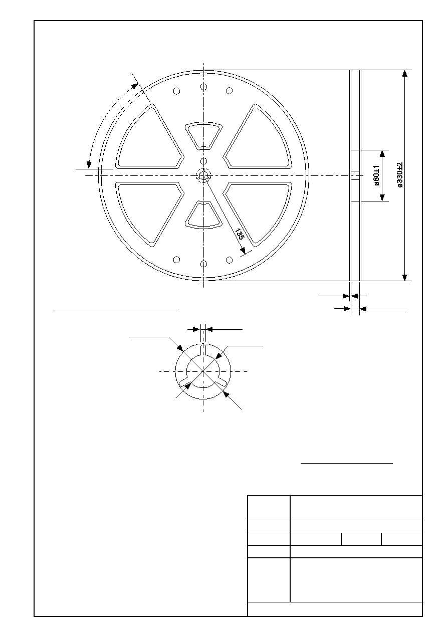
No. FJ008-A-P-SD-2.1
0.4Ī0.05
1.27
0.20Ī0.05
5.02Ī0.2
1
4
8
5
No.
TITLE
SCALE
UNIT
mm
SOP8J-A-PKG Dimensions
Seiko Instruments Inc.
FJ008-A-P-SD-2.1

No.
TITLE
SCALE
UNIT
mm
5
8
1
4
Ý2.0Ī0.05
Ý1.55Ī0.05
0.3Ī0.05
2.1Ī0.1
8.0Ī0.1
5įmax.
6.7Ī0.1
2.0Ī0.05
Seiko Instruments Inc.
Feed direction
4.0Ī0.1(10 pitches:40.0Ī0.2)
SOP8J-D-Carrier Tape
No. FJ008-D-C-SD-1.1
FJ008-D-C-SD-1.1
No.
TITLE
SCALE
UNIT
mm
QTY.
2,000
2Ī0.5
13.5Ī0.5
60į
2Ī0.5
Ý13Ī0.2
Ý21Ī0.8
Seiko Instruments Inc.
Enlarged drawing in the central part
SOP8J-D-Reel
No. FJ008-D-R-SD-1.1
FJ008-D-R-SD-1.1

∑
The information described herein is subject to change without notice.
∑
Seiko Instruments Inc. is not responsible for any problems caused by circuits or diagrams described herein
whose related industrial properties, patents, or other rights belong to third parties. The application circuit
examples explain typical applications of the products, and do not guarantee the success of any specific
mass-production design.
∑
When the products described herein are regulated products subject to the Wassenaar Arrangement or other
agreements, they may not be exported without authorization from the appropriate governmental authority.
∑
Use of the information described herein for other purposes and/or reproduction or copying without the
express permission of Seiko Instruments Inc. is strictly prohibited.
∑
The products described herein cannot be used as part of any device or equipment affecting the human
body, such as exercise equipment, medical equipment, security systems, gas equipment, or any apparatus
installed in airplanes and other vehicles, without prior written permission of Seiko Instruments Inc.
∑
Although Seiko Instruments Inc. exerts the greatest possible effort to ensure high quality and reliability, the
failure or malfunction of semiconductor products may occur. The user of these products should therefore
give thorough consideration to safety design, including redundancy, fire-prevention measures, and
malfunction prevention, to prevent any accidents, fires, or community damage that may ensue.