
Contents
Features .............................................................. 1
Applications ......................................................... 1
Block Diagram ..................................................... 1
Pin Assignment ................................................... 2
Description of Terminals ...................................... 2
Description of Operation ...................................... 3
Samples of Applied Circuits................................. 15
Dimensional Outline Diagram (Unit:mm).............. 16
Order Specification .............................................. 16
Adjastment of Oscillating Frequency ................... 17
Absolute Maximum Ratings ................................. 19
Recommended Operating Conditions .................. 19
Oscillation Characteristics ................................... 19
DC Electrical Characteristics ............................... 20
AC Electrical Characteristics ............................... 22
Sample of Properties (Reference values) ............ 25
Frequently Asked Questions.................................27

Seiko Instruments Inc.
1
S-3511A is a CMOS real-time clock IC , which is designed to transfer or
set each data of a clock and calender as requested by a CPU. It
provides connection with a CPU via three wires and has an
interrupt/alarm feature, allowing the alleviation of software treatment on
the side of a host.
It also works on lower power with the oscillating circuit operated at a
constant voltage. Its package uses an extremely small and thin type of
eight-pin SSOP.
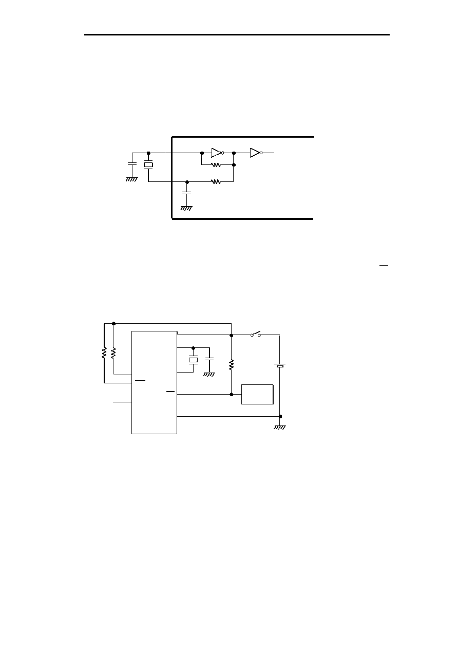
Block Diagram
Figure 1 Block diagram
Real-Time Clock
S-3511A
Features
Low power consumption
: 0.7
A typ. (V
DD
=3.0 V)
Wide area of operating voltage : 1.7 to 5.5 V
BCD input/output of year, month, day, day of a week, hour, minute and
second
CPU interface via three wires
Auto calender till the year of 2,099 (automatic leap year arithmetic feature
included)
Built-in power voltage detecting circuit
Built-in constant voltage circuit
Built-in flag generating circuit on power on/off
Built-in alarm interrupter
Steady-state interrupt frequency/duty setting feature
Built-in 32 KHZ crystal oscillating circuit (Internal Cd, External Cg)
8-pin SSOP package (terminal pitch: 0.65 mm)
Block Diagram
Applications
Cellular phone
PHS
A variety of pagers
TV set and VCR
Camera
INT Register
Status register
Oscillating
circuit
SCK
CS
Timing
generation
Power voltage
detecting
circuit
Constant
voltage
circuit
V
DD
V
SS
Comparator
Second
Minute
Hour
Day of
week
Day
Month
Year
Shift register
Serial
Interface
INT
XIN
XOUT
Clock
generating
circuit
SIO
Real-Time Clock
S-3511A
2
Seiko Instruments Inc.
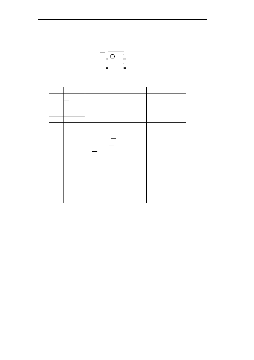
Pin Assignment
Description of Terminals
Terminal
Num.
Abbreviation
Description
Configuration
1
INT
Alarm interrupt output terminal.
Depending on the mode set by the INT
register and status register, it outputs low
or Clock when time is reached. It is
disabled by rewriting the status register.
N-channel open drain output
(No protective diode on the
side of VDD)
2
XIN
3
XOUT
Crystal oscillator connect terminal (32,768 HZ)
(Internal Cd, External Cg)
�
4
VSS
Negative power supply terminal (GND)
�
5
CS
Chip select input terminal.
During "H": The SIO terminal allows data
input/output.
The SCK terminal allows data
input.
During "L": The SIO terminal is in the High-Z
state.
The SCK terminal is in the input-disabled state.
CMOS input (Included pull-
down resistance. No
protective diode on the side
of VDD)
6
SCK
Serial clock input terminal.
The input/output of data from the SIO
terminal is performed in synchronization with
this clock. However, the clock is not accepted
while the CD terminal is "L."
CMOS input (No protective
diode on the side of VDD)
7
SIO
Serial data input/output terminal.
It is normally in the High-Z state while the
CS terminal is "L." When the CS terminal
changes from "L" to "H", the SIO terminal
is set to an input terminal. It will be set to
an input or output terminal, depending on
an subsequently input command.
N channel open drain output
(No protective diode aon the
side of VDD)
CMOS input
8
VDD
Positive power supply terminal.
�
Table 1 Description of terminals
Figure 2
Pin assignment
8-Pin SSOP
Top view
XOUT
VSS
6
5
8
7
3
4
1
2
SIO
VDD
SCK
CS
XIN
INT
Real-Time Clock
S-3511A
Seiko Instruments Inc.
3
Description of Operation
1.
Serial interface
S-3511A receives various commands via a three-wire serial interface to read/write data. This section covers the transfer methods of
this product.
1-1. Data reading
When you input data from the SIO terminal in synchronization with the falling of the SCK terminal after turning the CS
terminal to "H", the data is included into the inside of S-3511A at the eighth rising of the SCK clock and the state of data
reading is reached when the R/W bit has "1". The state leads to output of data corresponding each command in
synchronization with the falling of subsequent SCK clock input.
[Note] When the number of SCK clocks is less than eight, the state of clock waiting is reached and no processing is done.
When SCK clocks are more than required, they are processed in order from the first and the clocks other than
those required are ignored.
TEST
64
9
1
1
0
1
0
0
1
1
0
X
Output mode switching
(1) Real-time data reading 1
CS
SCK
SIO
9
1
CS
SCK
(3) Status register reading
Year data
Second data
1
1
0
0
0
1
1
0
X
Output mode switching
SIO
Status data
Input mode switching
LSB
MSB
Figure 3 Read communication
TEST
32
9
1
1
1
1
0
0
1
1
0
X
Output mode switching
(2) Real-time data reading 2
CS
SCK
SIO
Hour data
Second data
LSB
MSB
LSB
MSB
LSB
MSB
LSB
MSB
Input mode switching
Input mode switching
Command
Command
Command
LSB
MSB
LSB
MSB
LSB
MSB
POWER

Real-Time Clock
S-3511A
4
Seiko Instruments Inc.
1-2. Data writing
When you input data from the SIO terminal in synchronization with the falling of the SCK terminal after turning the CS
terminal to "H", the data is included into the inside of S-3511A at the eighth rising of the SCK clock and the state of data
reading is reached when the R/W bit has "0". In the state, the data is written to registers according each command in
synchronization with the falling of subsequent SCK clock input.
TEST
64
9
1
0
0
1
0
0
1
1
0
X
(1) Real-time data writing 1
CS
SCK
SIO
9
1
CS
SCK
(3) Status register writing
Year data
Second data
0
1
0
0
0
1
1
0
X
SIO
Status data
LSB
MSB
Figure 4 Write communication
TEST
32
9
1
0
1
1
0
0
1
1
0
X
(2) Real-time data writing 2
CS
SCK
SIO
Hour data
Second data
LSB
MSB
LSB
MSB
LSB
MSB
LSB
MSB
Command
Command
Command
MSB
LSB
MSB
LSB
MSB
LSB
POWER
Real-Time Clock
S-3511A
Seiko Instruments Inc.
5
1-3.Communication data configuration
After turning the CS terminal to "H", send four-bit fixed code "0110" and succeedingly transfer the command of a 3-bit
length and read/write command of a one-bit length.
2.
Command configuration
There are seven types of commands which read from and write to various registers. The table below lists them. Any
command that is not listed in the table provides no operation.
C2
C1
C0
Description
0
0
0
Reset (00 (year), 01 (month), 01 (day), 0 (day of week),
00 (minute), 00 (second)) (*1)
0
0
1
Status register access
0
1
0
Real-time data access 1 (year data to)
0
1
1
Real-time data access 2 (hour data to)
1
0
0
Alarm time/frequency duty setting 1
1
0
1
Alarm time/frequency duty setting 2
1
1
0
Test mode start (*2)
1
1
1
Test mode end (*2)
(*1) Don't care the R/W bit of this command.
(*2) This command is access-disabled due to specific use for the IC test.
Table 2 Command list
Figure 5 Communication data
Command
0
1
1
0
C2
C1
C0
R/W
Fixed code
MSB
LSB
Read/Write bit
Real-Time Clock
S-3511A
6
Seiko Instruments Inc.
2-1. Real-time data register
The real-time data register is a fifty-six-bit register which stores the BCD code of the data of year, month, day, day of week,
hour, minute and second. Any read/write operation performed by the real-time data access command sends or receives the
data from LSB on the first digit of the year data.
AM/
PM
Y80
Y40
Y20
Y10
Y8
Y4
Y2
Y1
MSB
LSB
Year data (00 to 99)
0
0
0
M10
M8
M4
M2
M1
MSB
LSB
Month data (01 to 12)
0
0
D20
D10
D8
D4
D2
D1
MSB
LSB
Day data (01 to 31)
0
0
0
0
0
W4
W2
W1
MSB
LSB
Day of week data (00 to 06)
A septenary counter. Set it so that it corresponds to the day
of the week.
0
H20
H10
H8
H4
H2
H1
MSB
LSB
Hour data (00 to 23 or 00 to 11)
0
MSB
LSB
Minute data (00 to 59)
TE
ST
S40
S20
S10
S8
S4
S2
S1
MSB
LSB
Second data (00 to 59) and test flag
m10
m8
m4
m2
m1
AM/PM : For 12-hour expression, 0:AM and 1:PM.
For 24-hour expression, this flag has no meaning
but either "0" or "1" must be written.
Sets the lower two digits of the Christian era (00 to 99) and
links together with the auto calender feature till 2,099.
The count value is automatically changed by the auto
calender feature:
1 to 31 :
1, 3, 5, 7, 8, 10, 12
1 to 30 :
4, 6, 9, 11
1 to 29 :
2 (leap year)
1 to 28 :
2 (common year)
TEST : Turns to "1" during the test mode.
Figure 6
Real-time data register
m20
m40

Real-Time Clock
S-3511A
Seiko Instruments Inc.
7
2-2. Status register
The status register is an eight-bit register which allows you to display and set various modes. The POWER flag is read-only
and others are read/write-enabled.
B7:POWER
This flag turns to "1" if the power voltage detecting circuit operates during power-on or changes in power
voltage (below VDET). Once turning to "1", this flag does not turns back to "0" even when the power
voltage reaches or exceeds the detected voltage. When the flag is "1", you must send the reset command
and turn it to "0". It is a read-only flag.
B6:12/24
This flag is used to set 12-hour or 24-hour expression.
0 : 12-hour expression
1 : 24-hour expression
B5:INTAE
This flag is used to choose the state of INT terminal output with interrupt output set. Enable this flag after
setting alarm time that forms a meeting condition in the INT register:
0 : Alarm interrupt output is disabled.
1 : Alarm interrupt output is enabled.
B3:INTME
This flag is used to make the output of the INT terminal per-minute edge interrupt or per-minute steady
interrupt. To make the output per-minute steady interrupt, set "1" at INTME and INTFE .
0 : Alarm interrupt or selected frequency steady interrupt output
1 : Per-minute edge interrupt or per-minute steady interrupt output
B1:INTFE
This flag is used to make the output of the INT terminal per-minute steady interrupt output (a period of one
minute, 50% of duty) or selected frequency steady interrupt. Note that the INT register is considered as the
data of frequency/duty if selected frequency steady interrupt is chosen.
0 : Alarm interrupt or selected frequency steady interrupt output
1 : Per-minute edge interrupt or per-minute steady interrupt output
B4, B2 and B0: If having written contents, they are ignored. When they are read, "0" can be read from them.
B7
LSB
POWER
12/24
INTAE
R
R/W
R/W
R/W
R/W
�
INTME
MSB
B6
B5
B4
B3
B2
B1
B0
�
INTFE
�
Figure 7 Status register

Real-Time Clock
S-3511A
8
Seiko Instruments Inc.
2-3. Alarm time/Frequency duty setting register
The alarm time/frequency duty setting register is a sixteen-bit register which sets alarm time or frequency duty. They are
switched by INTAE or INTFE register. AM/PM flag to be set must be in accordance with 12-hour or 24-hour expression. If
AM/PM flag is not rightly then set hour data is not met to alarm data.The alarm time/frequency duty setting register is a
write-only register.
(1)
When INTAE = 1
INT register is considered as alarm time data. Having the same configuration as the time and minutes registers of real-time
register configuration, they represent hours and minutes with BCD codes. When setting them, do not set any none-existent
day. Data to be set must be in accordance with 12-hour or 24-hour expression that is set at the status register.
(2) When INTFE = 1
INT register is considered as frequency duty data. By turning each bit of the registers to "1", a frequency corresponding to
each bit is chosen in an ANDed form.
AM/
PM
0
H8
H4
H2
H1
MSB
LSB
INT register
0
m8
m4
m2
m1
MSB
LSB
H20
H10
Figure 8 INT register (alarm)
m10
m20
m40
f0
MSB
LSB
INT register
MSB
LSB
f1
f2
f3
f4
f5
f6
f7
f8
f9
f10
f11
f12
f13
f14
f15
f0
f1
32768HZ
f2
f3
f4
f5
f6
f7
f8
f9
f10
f11
f12
f13
f14
f15
16384HZ
8192HZ
4096HZ
2048HZ
1024HZ
512HZ
256HZ
128HZ
8HZ
4HZ
2HZ
1HZ
64HZ
32HZ
16HZ
Figure 9 INT register (frequency duty)

Real-Time Clock
S-3511A
Seiko Instruments Inc.
9
2-4. Test flag
The test flag is a one-bit register which is assigned to MSB of the second data of the real-time data register. If a transferred
data is considered as the test mode starting data due to the receiving of the test mode starting data or noises, "1" is set.
When "1" is set, you must send the test mode ending command or reset command.
3.
Initialization
Note that S-3511A has different initializing operations, depending on states.
3-1. When power is turned on
Real-time data register :
00 (year), 01 (month), 01 (day), 0 (day of week), 00 (hour), 00 (minute), 00 (second)
Status register
:
"82h"
INT register
:
"8000h"
3-2. When the power voltage detecting circuits operates
The power voltage detecting circuit included in S-3511A operates and sets "1" at the bit 7 (POWER flag) of the internal
status register when power is turned on or power voltage is reduced. Once "1" is set, it is held even after the power voltage
gets equal to or higher than the detected power voltage. When the flag has "1", you must send the reset command from
CPU and initialize the flag. At this point, other registers does not change.
However, if the POWER flag has "0" during the power-on reset of CPU (S-3511A does not reach any indefinite area during
backup), you do not have to send the reset command.
3-3. When the reset command is received
When the reset command is received, each register turns as follows:
Real-time data register :
00 (year), 01 (month), 01 (day), 0 (day of week), 00 (hour), 00 (minute), 00 (second)
Status register
:
"00h"
INT register
:
"0000h"
32KHZ
Example
If f15 to f0 = 000AH
16KHZ
8KHZ
4KHZ
2KHZ
INT terminal output
Figure 10 Clock output
Set to frequency
duty mode
When power is turned on, the status register is set to "82h" and the INT register to "8000h" by the power-on detecting
circuit. In other words, "1" is sets at the bit 7 (POWER flag) of the status register and the clock of 1HZ is output from the INT
terminal. This is provided to adjust oscillating frequencies. In normal use, the reset command must be sent when power is
turned on.
Real-Time Clock
S-3511A
10
Seiko Instruments Inc.
4.
Processing of none-existent data and end-of-month
When writing real-time data, validate it and treat any invalid data and end-of-month correction.
[None-existent data processing]
Table 3 None-existent data processing
[End-of-month correction]
Any none-existent day is corrected to the first day of the next month. For example, February 30 is changed to March 1. Leap-
year correction is also performed here.
Register
Normal data
Error data
Result
Year data
00 to 99
XA to XF, AX to FX
00
Month data
01 to 12
00, 13 to 19, XA to XF
01
Day data
01 to 31
00, 32 to 39, XA to XF
01
Day of week data
0 to 6
7
0
Hour data (24-hour)
(*)
(12-hour)
0 to 23
0 to 11
24 to 29, 3X, XA to XF
12 to 19, XA to XF
00
00
Minute data
00 to 59
60 to 79, XA to XF
00
Second data (**)
00 to 59
60 to 79, XA to XF
00
Figure 11
Initializing
0
1 1
0
R
/
W
M
S
B
SIO LINE
0 0
1
L
S
B
1
command
status access command
VDD
POWER
flag
0
1 1
0
R
/
W
M
S
B
SIO LINE
0 0
1
L
S
B
1
command
VDD
POWER
flag
0
1
1
0
R
/
W
M
S
B
0 0
L
S
B
1
1
0 0
0 0 0
POWER flag
0
Don't care
backup state (S-3511A does not reach any indefinite area)
0
1 1
0
R
/
W
M
S
B
0 1
L
S
B
0
0 0
0 0 0
0
POWER flag
0
CPU down
reset command
status data
1
1
0
data
0
data
status access command
status data
command
command
real-time data access command
(*)
For 12-hour expression, write the AM/PM flag.
The AM/PM flag is ignored in 24-hour expression, but "0" for 0 to 11 o'clock and "1" for
12 to 23 o'clock are read in a read operation.
(**) None-existent data processing for second data is performed by a carry pulse one second
after the end of writing. At this point, the carry pulse is sent to the minute counter.
Real-Time Clock
S-3511A
Seiko Instruments Inc.
11
5.
Interrupt
Note 1 : If changing an output mode, give care to the state of the INT register and output.
Note 2 : If per-minute edge interrupt output or per-minute steady interrupt output is chosen, the INT register have no meaning.
NO.
INTAE
INTME
INTFE
Description
0
0
0
0
Output disabled
1
*
0
1
Selected frequency steady interrupt output
2
*
1
0
Per-minute edge interrupt output
3
*
1
1
Per-minute steady interrupt output
4
1
0
0
Alarm interrupt output
Note * : Don't care.
Table 4 Interrupt description
There are five types of output format from the INT terminal, which are selected by the INTAE, INTME and INTFE bits of the
status register.
(1) Alarm interrupt output
Alarm interrupt is enabled by setting hour and minute data to the INT register and turning the status register's INTAE to "1"
and INTME and INTFE to "0". When set hour data is met, low is output from the INT terminal. Since the output is held,
rewrite INTAE of the status register to "0" through serial communication to turn the output to high (OFF state).
(2) Selected frequency steady interrupt output
When you set frequency/duty data to the INT register and turn the status register's INTME to "0" and INTFE to "1" , clock set
at the INT register is output from the INT terminal.
(3) Per-minute edge interrupt output
When a first minute carry is performed after the status register's INTME is set with "1" and INTFE with "0", low is output from
the INT terminal. Since the output is held, rewrite INTAE, INTME and INTFE of the status register through a serial
communication. When you perform DISABLE or ENABLE communication while the minute carry processing signal is being
retained (for 10 msec), "Low" signal is output from the INT terminal again.
(4) Per-minute steady interrupt output
When a first carry is performed after the status register's INTME and INTFE are set with "1" , clock is output from the INT
terminal with a period of one minute (50% duty). When you perform DISABLE or ENABLE communication while the INT
terminal is at "L", "Low" signal is output from the INT terminal again.

Real-Time Clock
S-3511A
12
Seiko Instruments Inc.
Figure 12 Output mode
INTAE
INT terminal
INTME=INTFE=0
Alarm time corresponds
change by program
(1) Alarm interrupt output
INTFE
INT terminal
INTAE=INTME=0
Free run output starts
change by program
(2) Selected frequency steady interrupt output
INTME
INT terminal
INTAE=INTFE=0
(3) Per-minute edge interrupt output
INTFE,INTME
INT terminal
INTAE=0
(4) Per-minute steady interrupt output
OFF
OFF
INTFE
INT terminal
INTAE=INTME=0
Change by the reset command
(5 ) During power-on detecting circuit operation
OFF
0.5 second 0.5 second
OFF
"Low" signal is output again in case of
10 mSEC or less
Minute-carry processing
Minute-carry processing
Change by program
OFF
Change by program
Minute-carry
processing
Minute-carry processing
Minute-carry
processing
30 seconds
30 seconds
30 seconds
30 seconds
30 seconds
30 seconds
Real-Time Clock
S-3511A
Seiko Instruments Inc.
13
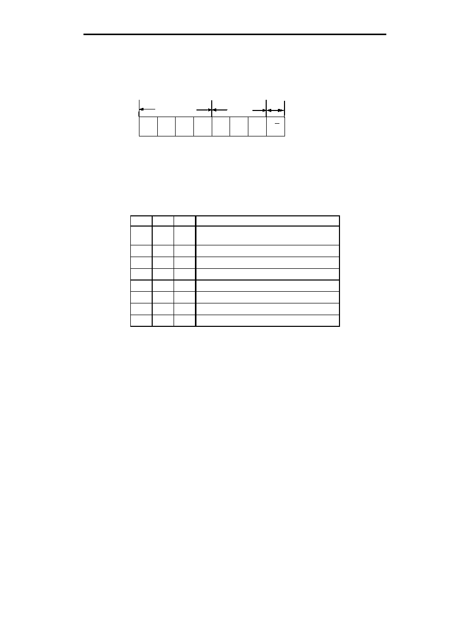
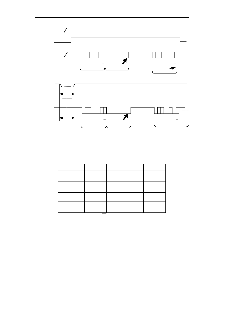
6.
Power voltage detecting circuit
S-3511A has an internal power voltage detecting circuit. This circuit gives sampling movement for only 15.6msec. once a second.
If the power voltage decreases below the detected voltage (VDET), sampling movement stops. Only when subsequent
communication is of the status read command, the output of the latch circuit is transferred to the sift register and the sampling
movement is resumed.
Decrease in power voltage can be monitored by reading the POWER flag.
That is to say, once decrease in power voltage is detected, any detecting operation is not performed and "H" is held unless you
perform initialization or send the status read command.
[Note]
When power voltage is increased and the first read operation is performed after decrease in power voltage occurs and the latch
circuit latches "H", "1" can be read on the POWER flag. However, if the next read operation is performed after the sampling of the
detecting circuit, the POWER flag is reset since sampling is subsequently allowed. See the timing diagram below.
Latch circuit
output
Sampling pulse
(0)
1sec
1sec
Stop
Stop
Stop
(1)
(1)
(1) (1)
(1) (1)
(0)
VDD
POWER flag
V
DET
Communication
Communication
Sampling pulse
Carry pulse
1sec
1sec
(1)
(0)
Latch circuit
output
POWER flag
[Timing of sampling pulse]
0.5sec
0.5sec
7.8mse
Carry-up timing
15.6mse
Latch timing
1Hz
V
DET
Sampling pulse
Stop
Stop
Stop
Stop
(1)
(0)
Figure 13 Timing of the power voltage detecting circuit
VDD

Real-Time Clock
S-3511A
14
Seiko Instruments Inc.
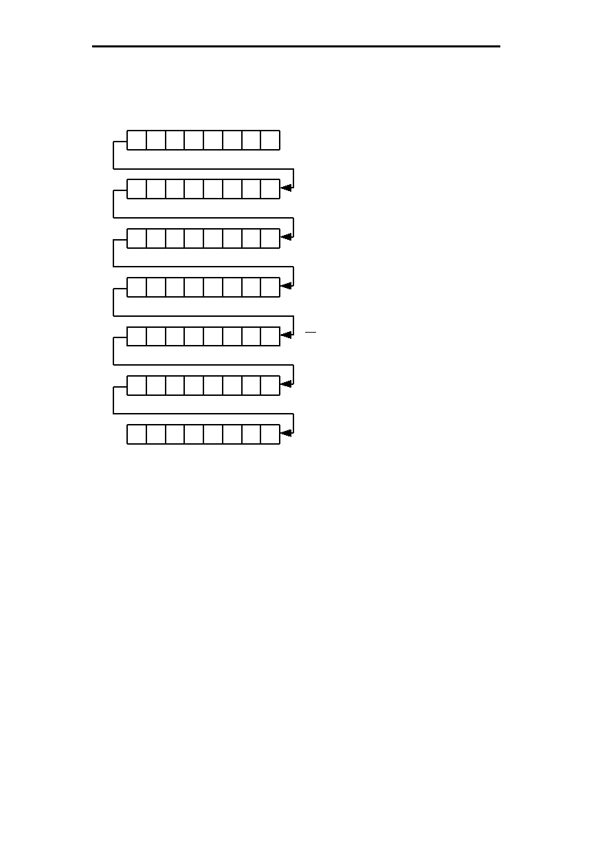
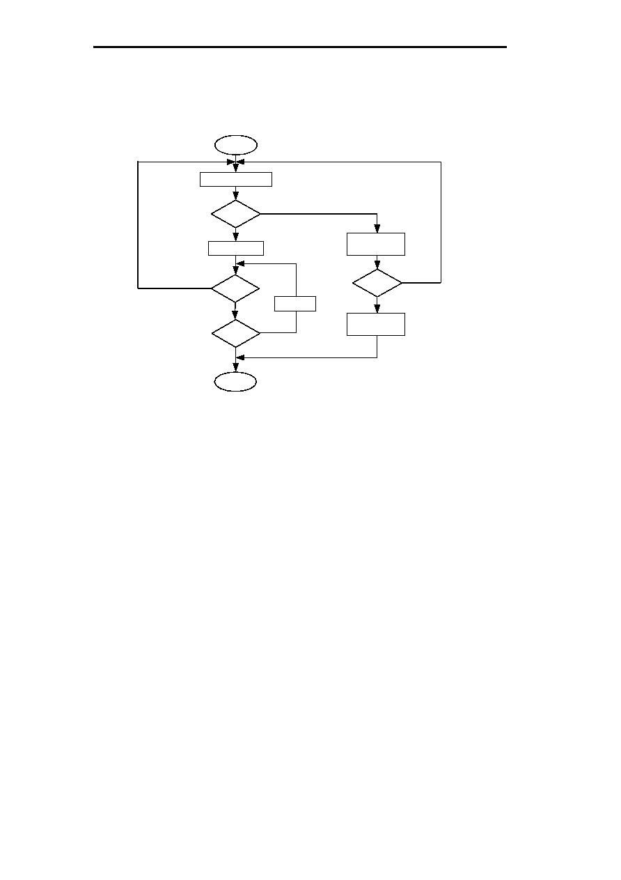
7.
Example of software treatment
(1 ) Initialization flow at power-on
NO
YES
START
END
POWER=1
(*1) If S-3511 is back-up and power is turned on only
on the CPU side, the reset command does not
need transferring.
(*2) If conditions are no good (e.g., noise) and probable
changes in commands occurs via serial
communications, it is recommended to make sure
the TEST flag.
(*3) The test ending command may be used alternately
Power on
Reset command
transfer
NO
YES
TEST=1
Reset command
transfer
Status register setting
command transfer
Real-time data setting
command transfer
INT register setting
command transfer
(*1)
(*2)
(*3)
Figure 14 Initialization flow

Real-Time Clock
S-3511A
Seiko Instruments Inc.
15
Samples of Applied Circuits
Vcc
X
OUT
X
IN
S-3511AEFS
SIO
Vss
V
DD
SCK
Vss
Vcc
External CPU
INT
System
power
Cg
Due to the I/O terminal with no protective diode on the VDD side, the relation of VCC
VDD has
no problem. But give great care to the standard.
Make communications after the system power is turned on and a stable state is obtained.
Figure 15 Applied circuit 1
CS
Make communications after the system power is turned on and a stable state is obtained.
Vss
Vcc
External CPU
Power
switching
circuit
X
OUT
X
IN
S-3511AEFS
Vss
V
DD
System
power
Figure 16 Applied circuit 2
Cg
INT
SIO
SCK
CS
Real-Time Clock
S-3511A
16
Seiko Instruments Inc.
Dimensional Outline Diagram (Unit: mm)
Eight-pin SSOP
Order Specification
4.4
3.12 (3.42 max.)
6.4
0.3
Figure 17 Dimensional outline diagram
0.65
0.22
0.10
1.15
0.05
1.30max.
0.05
0.05
0.15
+0.10
�0.05
0.5
0.2
S-3511AE
FS
Package (fixed)
: Eight-pin SSOP
Description (fixed)
Real-Time Clock
S-3511A
Seiko Instruments Inc.
17
Adjustment of Oscillating Frequency
1.
Configuration of the oscillating circuit
Since crystal oscillation is sensitive to external noises (clock accuracy is affected), the fallowing measures must be taken in configuring
the oscillating circuit:
(1) S-3511A, crystal oscillator and external capacitor (Cg) are placed as close to each other as possible.
(2) Make high the insulation resistance between terminals and the board between XIN and XOUT.
(3) Do not place any signal or power lines close to the oscillating circuit.
2.
Measurement of oscillating frequencies
(*) If the error range is �1ppm in relation to 1HZ, time is shifted by approximately 2.6 seconds a month:
10
-6(1ppm)
60 seconds
60 minutes
24 hours
30 days = 2.592 seconds
XIN
XOUT
Cg
S-3511A
Figure 18 Connection diagram
Cd
Rd
Rf
Crystal oscillator:32.768KHZ
CL=6pf
Cg=3 to 35pf
Oscillating circuit internal constant standard values:
Rf=20M
Rd=220K
Cd=12pf
When power is turned on, S-3511A has the internal power-on detecting circuit operating and outputs a signal of 1HZ from the INT
terminal to select the crystal oscillator and optimize the Cg value. Turn power on and measure the signal with a frequency counter
following the circuit configuration shown in Figure 22. Refer to 9 and 12 pages in this document for further information.
INT
Frequency
counter
VDD
XIN
XOUT
SIO
VSS
CS
SCK
Cg
Open
S-3511A
Note 1: Use a high-accuracy frequency
counter (1ppm order).
Note 2: Since the 1HZ signal continues
to be output, you must send the
reset command in normal
operation.
Note 3: Determine Cg with its
frequency slow/fast range
property referred.
Figure 19 Connection diagram
Real-Time Clock
S-3511A
18
Seiko Instruments Inc.
3.
Adjustment of oscillating frequencies
Matching of a crystal oscillator with the nominal frequency must be performed with suspended capacity on the board included. Select a
crystal oscillator and optimize the Cg value in accordance with the flow chart below.
(*1)
For making matching adjustment of the IC with a crystal, contact an appropriate crystal maker to determine the CL value
(load capacity) and RI value (equivalent serial capacity). The CL value = 6pf and RI value = 30K
TYP. are recommended
values.
(*2)
Cg value selection must be performed on the actual PCB since suspended capacity affects it. Select the Cg value in a
range from 3pf to 35pf. If the frequency does not match, change the CL value of the crystal.
(*3)
Adjust the rotation angle of the variable capacity so that the capacity value is somewhat smaller than the center, and
confirm the oscillating frequency and the center value of the variable capacity. This is done in order to make the capacity of
the center value smaller than one half of the actual capacity value because a smaller capacity value makes a greater
quantity of changes in a frequency. If the frequency does not match, change the CL value of the crystal.
Note 1 : Oscillating frequencies are changed by ambient temperature and power voltage. Refer to property samples.
Note 2 : The 32KHZ crystal oscillator operates slower at higher or lower ambient temperature than 20 to 25�C. Therefore, it is
recommended to adjust or set the oscillator to operate somewhat faster at normal temperature.
NO
YES
START
Variable
capacity
Select a crystal oscillator.
NO
Is Cg in the
specification
?
(*1)
(*2)
Cg set
NO
Is it an
optimal
value ?
YES
Change Cg.
END
YES
Set to the center of
variable capacitor.
Does
the frequency
match ?
NO
YES
Make fine adjustment of the
frequency in variable capacity.
(*3)
(*3)
<Trimer capacitor>
<Fixed capacitor>
Real-Time Clock
S-3511A
Seiko Instruments Inc.
19
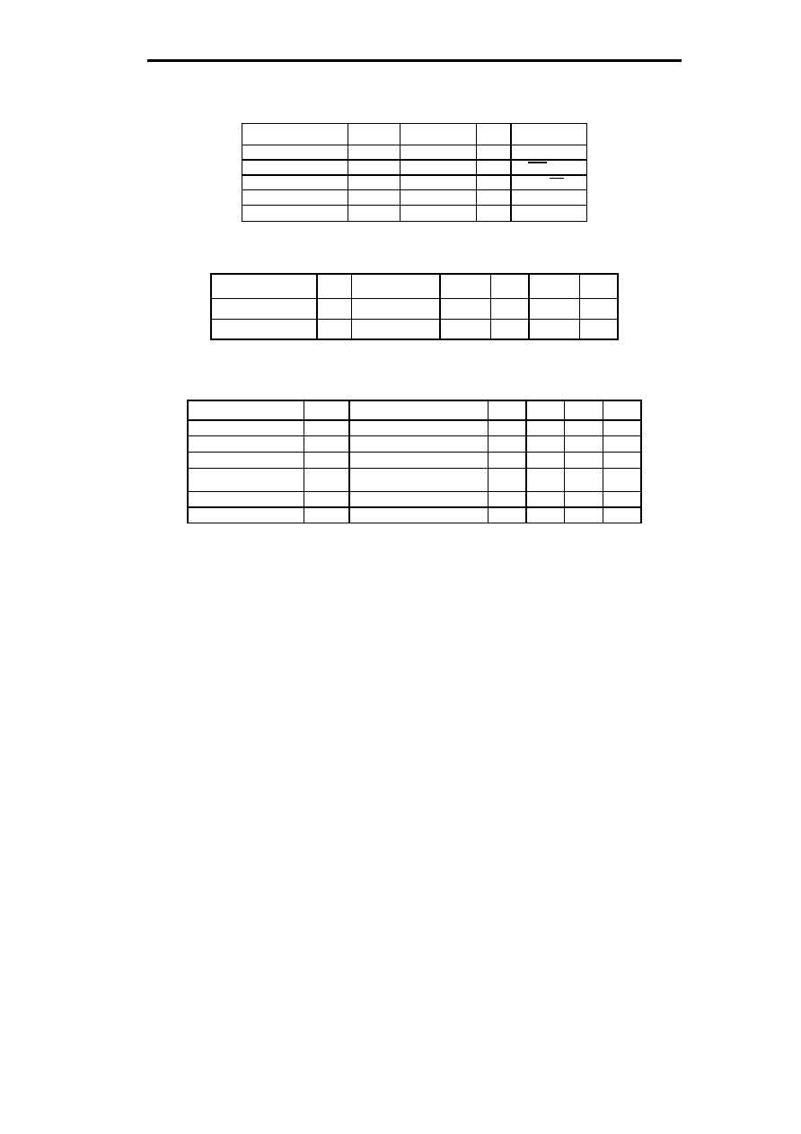
Absolute Maximum Ratings
Table 5 Absolute maximum ratings
Item
Symbol
Rating
Unit
Applicable terminal,
conditions
Power voltage
VDD
�0.3 to +6.5
V
--
Input voltage
V
IN
�0.3 to +6.5
V
SCK, SIO
Output voltage
V
OUT
�0.3 to +6.5
V
SIO, INT
Operating temperature
T
opr
�40 to +85
�C
VDD=3.0V
Retention temperature
T
stg
�55 to + 25
�C
--
Recommended Operating Conditions
Table 6 Recommended operating conditions
Item
Symbol
Condition
Min.
Typ.
Max.
Unit
Power voltage
VDD
--
1.7
3.0
5.5
V
Operating temperature
T
opr
--
�20
+25
+70
�C
Oscillation Characteristics
Table 7 Oscillation characteristics
(Ta=25�C, VDD=3V, DS-VT-200 (crystal oscillator, CL=6pF, 32,768HZ) manufactured by Seiko Electronic Part Co., Ltd.)
Item
Symbol
Condition
Min.
Typ.
Max.
Unit
Oscillation start voltage
V
STA
Within ten seconds
1.7
--
5.5
V
Oscillation start time
T
STA
--
--
--
1
SEC
IC-to-IC frequency diversity
IC
--
�10
--
+10
ppm
Frequency voltage
diversity
V
VDD=1.7 to 5.5V
�3
--
+3
ppm/V
Input capacity
Cg
Applied to the XIN terminal
3
--
35
pF
Output capacity
Cd
Applied to the XOUT terminal
---
12
--
pF
Real-Time Clock
S-3511A
20
Seiko Instruments Inc.
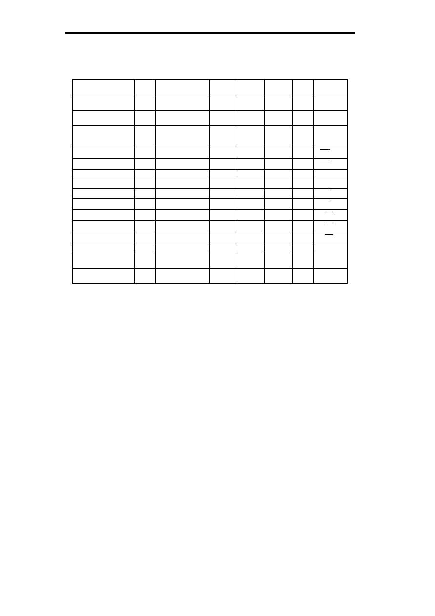
DC Electrical Characteristics
Table 8 DC characteristics (3V)
Item
Symbol
Condition
Min.
Typ.
Max.
Unit
Applicable
terminal
Range of operating
voltage
VDD
Ta = �20 to+70�C
1.7
3.0
5.5
V
--
Drain current 1
I
DD1
During no
communications
--
0.7
1.5
A
--
Drain current 2
I
DD2
During
communications
(SCL=100KHZ)
--
5.5
10
A
--
Input leak current 1
I
ILL1
V
IN
= VDD
�0.5
--
0.5
A
SCK,SIO
Input leak current 2
I
ILL2
V
IN
= VSS
�0.5
--
0.5
A
SCK,SIO
Input current 1
I
IL1
V
IN
=5.5V
2
6
20
A
CS
Input current 2
I
IL2
V
IN
=0.4V
40
110
300
A
CS
Output leak current1
I
OZH
V
OUT
=VDD
�0.5
--
0.5
A
INT, SIO
Output leak current2
I
OZL
V
OUT
=VSS
�0.5
--
0.5
A
INT, SIO
Input voltage 1
V
IH
--
0.8xVDD
--
--
V
SIO, SCK, CS
Input voltage 2
V
IL
--
--
--
0.2xVDD
V
SIO, SCK, CS
Output current 1
I
OL1
V
OUT
=0.4V
1.5
2.5
--
mA
INT
Output current 2
I
OL2
V
OUT
=0.4V
5
10
--
mA
SIO
Power voltage detecting
voltage 1
V
DET1
Ta=+25�C
1.8
2.0
2.2
V
--
Power voltage detecting
voltage 2
V
DET2
Ta= �20 to+70�C
1.72
--
2.3
V
--
(Ta=25�C,VDD=3V,DS-VT-200 (crystal oscillator, CL=6pF, 32,768HZ) manufactured by Seiko Electronic Part Co., Ltd.)
Real-Time Clock
S-3511A
Seiko Instruments Inc.
21
Table 9 DC characteristics (5V)
Item
Symbol
Condition
Min.
Typ.
Max.
Unit
Applicable
terminal
Range of operating
voltage
VDD
Ta = �20 to+70�C
1.7
3.0
5.5
V
--
Drain current 1
I
DD1
During no
communications
--
1.6
3.0
A
--
Drain current 2
I
DD2
During
communications
(SCL=100KHZ)
--
12
20
A
--
Input leak current 1
I
ILL1
V
IN
= VDD
� 0.5
--
0.5
A
SCK,SIO
Input leak current 2
I
ILL2
V
IN
= VSS
� 0.5
--
0.5
A
SCK,SIO
Input current 1
I
IL1
V
IN
=5.5V
10
25
50
A
CS
Input current 2
I
IL2
V
IN
=0.4V
100
175
400
A
CS
Output leak current1
I
OZH
V
OUT
=VDD
� 0.5
--
0.5
A
INT, SIO
Output leak current2
I
OZL
V
OUT
=VSS
� 0.5
--
0.5
A
INT, SIO
Input voltage 1
V
IH
--
0.8xVDD
--
--
V
SIO, SCK, CS
Input voltage 2
V
IL
--
--
--
0.2xVDD
V
SIO, SCK, CS
Output current 1
I
OL1
V
OUT
=0.4V
2.0
3.5
--
mA
INT
Output current 2
I
OL2
V
OUT
=0.4V
6
12
--
mA
SIO
Power voltage detecting
voltage 1
V
DET1
Ta=+25�C
1.8
2.0
2.2
V
--
Power voltage detecting
voltage 2
V
DET2
Ta= �20 to+70�C
1.72
--
2.3
V
--
(Ta=25�C, VDD=3V, DS-VT-200 (crystal oscillator, CL=6pF, 32,768HZ) manufactured by Seiko Electronic Part Co., Ltd.)

Real-Time Clock
S-3511A
22
Seiko Instruments Inc.
AC Electrical Characteristics
Table 10 AC characteristics 1
(S-3511A, RL=10K
, CL=80pF)
Conditions: VDD = 1.7V to 5.5V, Ta = �20 to 70�C
Input; V
IH
=0.8
VDD, V
IL
=0.2
VDD, Output; V
OH
=0.8
VDD, V
OL
=0.2
VDD
Item
Symbol
Min.
Typ.
Max.
Unit
Clock pulse width
t
SCK
5
--
250000
s
Setup time before CS rising
t
DS
1
--
--
s
Hold time after CS rising
t
CSH
1
--
--
s
Input data setup time
t
ISU
1
--
--
s
Input data hold time
t
IHO
1
--
--
s
Output data definition time
t
ACC
--
--
3.5
s
Setup time before CS falling
t
CSS
1
--
--
s
Hold time after CS falling
t
DH
1
--
--
s
Input rising/falling time
t
R
,
t
F
--
--
0.1
s
Note:
Since the output form of the SIO terminal is N-channel open drain output, the rising time of t
ACC
is
determined by the values of load resistance (RL) and load capacity (CL) outside the IC. Use this as
a reference value.
Table 11
AC characteristics 2
(S-3511A, RL=10K
, CL=80pF)
Conditions ; VDD=3.0
0.3V, Ta=-20~70�C
Input ; V
IH
=0.8
VDD, V
IL
=0.2
VDD, Output ; V
OH
=0.8
VCC, V
OL
=0.2
VCC(VCC=5.0V)
Item
Symbol
Min.
Typ.
Max.
Unit
Clock pulse width
t
SCK
1
--
250000
s
Setup time before CS rising
t
DS
0.2
--
--
s
Hold time after CS rising
t
CSH
0.2
--
--
s
Input data setup time
t
ISU
0.2
--
--
s
Input data hold time
t
IHO
0.2
--
--
s
Output data definition time
t
ACC
--
--
1.0
s
Setup time before CS falling
t
CSS
0.2
--
--
s
Hold time after CS falling
t
DH
0.2
--
--
s
Input rising/falling time
t
R
,
t
F
--
--
0.05
s
Note:
Since the output form of the SIO terminal is N-channel open drain output, the rising time of t
ACC
is
determined by the values of load resistance (RL) and load capacity (CL) outside the IC. Use this as
a reference value
.

Real-Time Clock
S-3511A
Seiko Instruments Inc.
23
Table 12
AC characteristics 3
(S-3511A,RL=10K
, C
L
=80pF)
Conditions: VDD=5.0
0.5V, Ta=-20 to 70�C
Input; V
IH
=0.8
VDD, V
IL
=0.2
VDD, Output; V
OH
=0.8
VDD, V
OL
=0.2
VDD
Item
Symbol
Min.
Typ.
Max.
Unit
Clock pulse width
t
SCK
0.5
--
250000
s
Setup time before CS rising
t
DS
0.1
--
--
s
Hold time after CS rising
t
CSH
0.1
--
--
s
Input data setup time
t
ISU
0.1
--
--
s
Input data hold time
t
IHO
0.1
--
--
s
Output data definition time
t
ACC
--
--
0.3
s
Setup time before CS falling
t
CSS
0.1
--
--
s
Hold time after CS falling
t
DH
0.1
--
--
s
Input rising/falling time
t
R
,
t
F
--
--
0.05
s
Note:
Since the output form of the SIO terminal is N-channel open drain output, the rising time of t
ACC
is
determined by the values of load resistance (RL) and load capacity (CL) outside the IC. Use this as
a reference value.
Real-Time Clock
S-3511A
24
Seiko Instruments Inc.
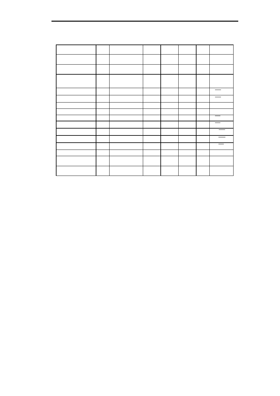
t
DH
t
DH
t
CSS
t
DS
CS
SCK
SIO
t
DS
t
CSH
80%
80%
20%
20%
50%
20%
80%
20%
20%
80%
t
ACC
t
SCK
t
SCK
t
R
,
t
F
t
F
t
R
t
ISU
SCK
Input data
t
IHO
50%
SCK
Output data

Real-Time Clock
S-3511A
Seiko Instruments Inc.
25
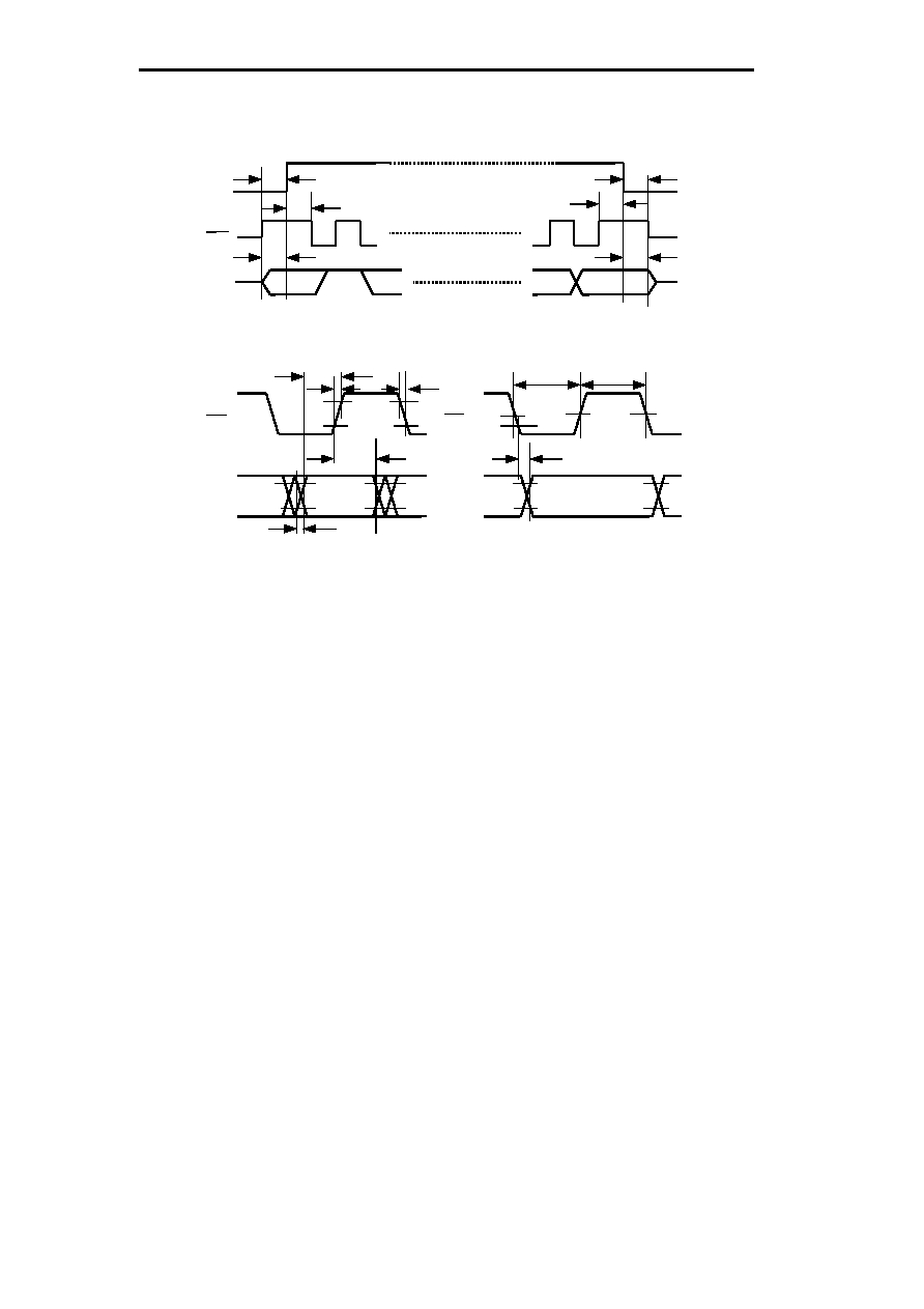
Sample of Properties (Reference values)
(1) Standby current versus Cg
Ta=25�C
(2) Standby current versus VDD
Ta=25�C
(3) Operating drain current versus Input clock
Ta=25�C
(4) Standby current versus temperature
(5) Oscillating frequency versus Cg
Ta=25�C
(6) Oscillating frequency versus VDD
SCK frequency
0
5
10
15
0
0.5
1
1.5
2
Cg
[pf]
IDD1
[uA]
0
1
2
3
4
5
6
0
0.5
1
1.5
2
2.5
3
IDD1
[uA]
VDD
[V]
Ta
[�C]
-30
-10
10
30
50
80
0
0.5
1
1.5
2
IDD1
[uA]
0
400
1,000
0
50
100
150
IDD2
[uA]
Ta=25�C
VDD
[V]
0
2
4
6
-4
-2
0
2
4
f/f
[ppm]
Cg
[pf]
f/f
[ppm]
0
5
10
15
-20
0
20
40
60
80
VDD=5V
VDD=3V
VDD=5V
VDD=3V
VDD=5V
VDD=3V
VDD=3V
VDD=5V
Real-Time Clock
S-3511A
26
Seiko Instruments Inc.
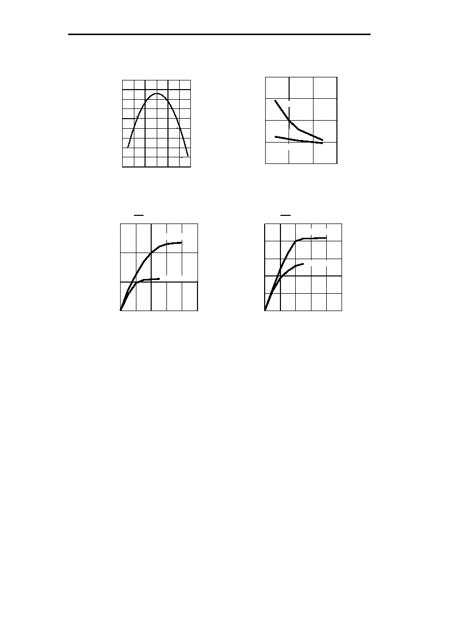
(8) Oscillation start time versus Cg
(9) Output current 1 (VDS versus IDS)
INT terminals,Ta=25
�C
(7) Oscillating frequency versus temperature
(10) Output current 2 (VDS versus IDS)
SIO terminal,Ta=25
�C
Ta=25
�C
Cg
[pf]
T
STA
[mS]
0
5
10
15
0
200
400
600
800
-50
0
50
100
-160
-120
-80
-40
20
Ta=25
�C,VDD=3V
Ta
[�C]
f/f
[ppm]
VDS
[V]
IDS
[mA]
0
1
2
3
4
5
0
10
20
30
40
50
VDS
[V]
0
1
2
3
4
5
0
5
10
15
IDS
[mA]
VDD=5V
VDD=3V
VDD=5V
VDD=3V
VDD=5V
VDD=3V

27
Collection of Product FAQs
Author: Shirai Masaaki
Date: 99/04/16 (Friday) 18:20 (modified: 99/04/16(Friday))
<Information level>
A:
Public (Printing O.K.)
Index:
B: General
<Product>
Division name: 01 IC
Category 1:
17 ASSP
Category 2:
2. Real-Time Clock
Product name: Overall
Related documents:
Question:
What are the notes for time settings (S3511/S3530/S3531)?
Answer:
If time data is rewritten in a product with an alarm interrupt (S-3511/S-3530/S-3531), be sure to disable
the alarm interrupt before the time is set.
Reason: When data is written using real-time data access 2, registers for hours, minutes, and seconds
are reset (all "0"'s), and arbitrary hours, minutes, and seconds are then set. If the alarm is set for 0:00
a.m. and the alarm interrupt is enabled, when the time data is rewritten the registers are reset (all "0"'s)
to 0:00 a.m., the set alarm time, thereby causing an interrupt (INT).
<Remarks>
FAQ No.: 17S35004

28
Collection of Product FAQs
Author: Shirai Masaaki
Date: 99/04/14 (Wednesday) 11:34 (modified: 99/05/18)
<Information level>
A:
Public (Printing O.K.)
Index:
B: Technical
<Product>
Division name: 01 IC
Category 1:
17 ASSP
Category 2:
2. Real-Time Clock
Cal No.:
Overall
Related documents:
Question:
What about the write/read errors (notes)?
Answer:
To continuously write or read data in a 3-wire RTC (S-3511/S-3513/S-35L12/S-3510), be sure to change
"CS" to "L" after the first command has been executed and before the next command is executed. If
commands are continuously executed without changing "CS" to "L," the second command is
disregarded.
Be sure to change
"CS" to "L."
CS
SCK
0
1
0
0
0
1
1
0
X
SIO
Status data
LSB
MSB
Command
MSB
LSB
POWER
9
1
0
1
1
0
0
1
1
0
X
Time data
LSB
MSB
Command
MSB
LSB
<Remarks>
FAQ No.: 17S35003

29
Collection of Product FAQs
Author: Shirai Masaaki
Date: 99/04/13 (Tuesday) 15:40 (modified: 99/05/18)
<Information level>
A:
Public (Printing O.K.)
Index:
A: General
<Product>
Division name: 01 IC
Category 1:
17 ASSP
Category 2:
2. Real-Time Clock
Cal No.:
Overall
Related documents:
Question:
What about the Y2K problem?
Answer:
Our Real-Time Clock outputs information consisting of the last two digits of the year. The S-35L12/L32
can use the register bits in its RTC to determine whether the year is 1900 or 2000 when the last two
digits change from 99 to 00. Most other RTCs, however, cannot determine whether the year is 1900 or
2000 when the last two digits change from 99 to 00. Thus, when this microcomputer is used, the user
must load year information for the RTC in a microcomputer to determine whether the year is 1900 or
2000. Accordingly, when the year reaches 2000, our RTC allows year information to operate normally
and be output as "00," thereby preventing malfunctions.
There is no problem with the operation of the IC. If, however, peripheral circuits and software
developed by a client manage year information using the last two digits of the year, they may
malfunction. Thus, such devices should be checked.
<reference>
http://www.sii.co.jp/sii2000.htm
<Remarks>
FAQ No.: 17S35002

30
Collection of Product FAQs
Author: Shirai Masaaki
Date: 99/04/13 (Tuesday) 14:26 (modified: 99/04/13)
<Information level>
A:
Public (Printing O.K.)
Index:
A: General
<Product>
Division name: 01 IC
Category 1:
17 ASSP
Category 2:
2. Real-Time Clock
Cal No.:
Overall
Related documents:
Question:
Why is an auto calendar available through the year 2099?
Answer:
The SII's RTC denotes the year using its last two digits. These digits are then divided by four, and if
they are divisible the year is determined to be a leap year (the auto calendar determines both 1996 and
2000 to be leap years). The actual calendar, however, does not treat a year with "00" as its last two
digits as a leap year (except for the year 2000; see the following). Accordingly, although 2100 is not a
leap year, the RTC treats it as one. Therefore, this auto calendar is available through 2099.
(Note) A year is defined as a leap year when its last two digits are "00" and its first two digits are
divisible by four.
<Remarks>
FAQ No.: 17S35001