 | –≠–ª–µ–∫—Ç—Ä–æ–Ω–Ω—ã–π –∫–æ–º–ø–æ–Ω–µ–Ω—Ç: S-35L32A | –°–∫–∞—á–∞—Ç—å:  PDF PDF  ZIP ZIP |
Document Outline
- S-35L32A
- Cover
- Features
- Applications
- Package
- Block Diagram
- Product Code Structure
- Pin Assignment
- Description of Pins
- Absolute Maximum Ratings
- Recommended Operating Conditions
- Oscillation Characteristics
- DC Electrical Characteristics
- AC Electrical Characteristics
- Description of Operation
- Samples of Application Circuits
- Adjustment of Oscillating Frequency
- Precautions
- Characteristics (Reference Data)
- Package Drawing

Rev. 1.3
_00
REAL-TIME CLOCK
S-35L32A
Seiko
Instruments
Inc.
1
S-35L32A is a CMOS real-time clock IC supporting an
I
2
C-BUS, which is designed to transfer or set each data of
a clock and calendar as requested by a CPU.
The S-35L32A is interfaced with a CPU via two wires (I
2
C-
BUS). Two systems of an interrupt/alarm function and 32
kHz-fixed clock output make it easy to develop and
process software at the side of a host computer. It also
works on lower power with the oscillating circuit operated
at a constant voltage.
Features
∑ Low power consumption
:0.55
µA typ. (V
DD
=3.0 V)
∑ Wide area of operating voltage :1.3 to 3.6 V
(1.65 to 3.6 V with the power voltage detection circuit built-in)
∑ BCD input/output of year, month, day, day of a week, hour, minute and second
∑ CPU interface via two wires (I
2
C-BUS)
∑ Auto calender till the year of 2,099
(automatic leap year arithmetic feature included)
∑ Built-in power voltage detecting circuit
∑ Built-in constant voltage circuit
∑ Built-in flag generating circuit on power on/off
∑ Built-in alarm interrupter (two systems)
∑ 32 kHz-fixed clock output
∑ Steady-state interrupt frequency/duty setting feature
∑ Built-in 32 kHz crystal oscillating circuit (Internal Cd, External Cg)
Applications
∑ Cellular phone
∑ PHS
∑ A variety of pagers
∑ TV set and VCR
∑ Camera
Package
∑ 10-Pin SSOP (pin pitch : 0.5 mm) (Package drawing code : FS010-A)
∑ Die
REAL-TIME CLOCK
S-35L32A
Rev.1.3
_00
2
Seiko Instruments Inc.
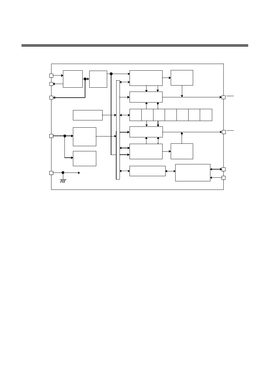
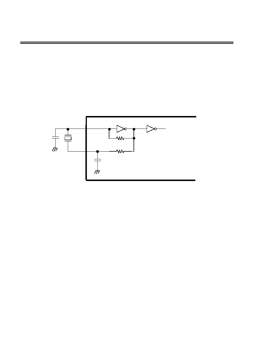
Block Diagram
INT1 Register
Status register
Oscillating
circuit
SCL
SDA
Timing
generation
Power
voltage
detecting
circuit
Constant
voltage
circuit
F32K
VDD
VSS
Comparator 1
Second
Minute
Hour
Day of
week
Day
Month
Year
Shift register
I
2
C-BUS
Interface
INT1
XIN
XOUT
Clock
generating
circuit
Comparator 2
INT2
INT2 Register
Clock
generating
circuit
Figure 1

REAL-TIME
CLOCK
Rev.1.3
_00
S-35L32A
Seiko
Instruments
Inc.
3
Product Code Structure
S-35L32AE
xx
Package name (abbreviation)
FS: 10-Pin SSOP10
CA: Die
Description (fixed)
REAL-TIME CLOCK
S-35L32A
Rev.1.3
_00
4
Seiko Instruments Inc.
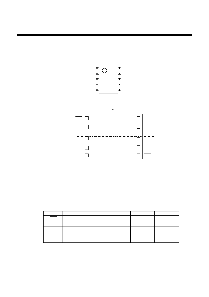
Pin Assignment
(1) Package: S-35L12AEFS
10-Pin SSOP
Top view
XOUT
VSS
F32K
8
7
6
10
9
3
4
5
1
2
SDA
VDD
SCL
INT2
N.C
INT1
XIN
Figure 2
(2) Die : S-35L12AECA
INT2
SCL
N.C
SDA
VDD
VSS
F32k
XOUT
XIN
INT1
X
S
-
35L32A
Y
0
Remark
Die size : 1.94
◊ 1.58 mm
Sizes shown are for design purposes only.
The corners of the die shrink by approximately 30
µm after dicing.
Pad size : 100
◊ 100 µm
Chip rear area potential : VSS
Do not wire-bonding to the N.C. pin.
Pad Coordinates
Symbol X-Coordinate Y-Coordinate Symbol X-Coordinate Y-Coordinate
INT1
-811 631
VDD
811 631
XIN
-811 330 SDA 811 393
XOUT
-811 29 SCL
811
-29
VSS
-811
-375 NC 811 -209
F32k
-811
-631 INT2 811 -631
Figure 3
REAL-TIME
CLOCK
Rev.1.3
_00
S-35L32A
Seiko
Instruments
Inc.
5
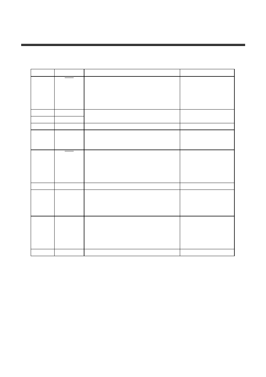
Description of Pins
Table 1
Pin No.
Symbol
Description
Configuration
1 INT1
Alarm interrupt 1 output pin.
Depending on the mode set by the INT1
register and status register, it outputs low or
Clock when time is reached. It is disabled by
rewriting the status register.
Nch open drain output (No
protective diode at the side
of VDD)
2 XIN
3 XOUT
Crystal oscillator connect pin (32,768 Hz)
(Internal Cd, External Cg)
-
4
VSS
Negative power supply pin (GND)
-
5 F32K
32,768 Hz clock output pin
Nch open drain output (No
protective diode at the side
of VDD)
6 INT2
Alarm interrupt 2 output pin.
Depending on the mode set by the INT2
register and status register, it outputs low or
Clock when time is reached. It is disabled by
rewriting of the status register.
Nch open drain output (No
protective diode at the side
of VDD)
7
NC
*1
No connection
-
8
SCL
Serial clock input pin.
Follow the specification with great care to the
rising/falling time of the SCL signal because
the signal is treated at its rising/falling edge.
CMOS input (No protective
diode at the side of VDD)
9 SDA
Serial data input/output pin.
This pin is usually pulled up to VDD via a
resistor, and connected to other open-drain or
open-collector output devices in wired OR
configuration.
Nch open drain output (No
protective diode at the side
of VDD)
CMOS input
10
VDD
Positive power supply pin.
-
*1. NC indicates that the pin is electrically open, therefore the pin can be connected to VDD or VSS.
REAL-TIME CLOCK
S-35L32A
Rev.1.3
_00
6
Seiko Instruments Inc.
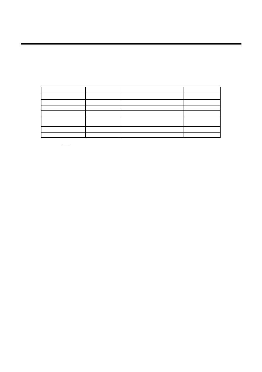
Absolute Maximum Ratings
Table 2
Item
Symbol
Applicable pin, conditions
Rating
Unit
Power voltage
V
DD
-
V
SS
-0.3 to V
SS
+4.0 V
Input voltage
V
IN
Applied
to
SCL,SDA V
SS
-0.3 to V
SS
+4.0 V
Output voltage
V
OUT
Applied to SDA,INT1, INT2
V
SS
-0.3 to V
SS
+4.0 V
Storage temperature
T
stg
-
-55 to +125
∞C
Caution The absolute maximum ratings are rated values exceeding which the product
could suffer physical damage. These values must therefore not be exceeded
under any conditions.
Recommended Operating Conditions
Table 3
Item
Symbol
Condition Min.
Typ.
Max.
Unit
Power voltage
V
DD
- 1.3
3.0
3.6
V
Operating temperature
T
opr
-
-20
+25
+70
∞C
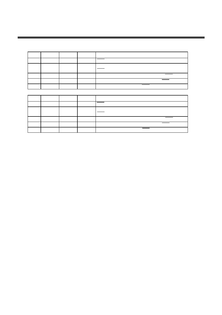
Oscillation Characteristics
Table 4
(Unless otherwise specified : Ta
=25∞C, V
DD
=3 V, DS-VT-200 (crystal oscillator, C
L
=6 pF, 32,768 Hz) manufactured by SII Quartz Techno Ltd.)
Item Symbol
Condition
Min.
Typ.
Max.
Unit
Oscillation start voltage
V
STA
Within ten seconds
1.3
- 3.6 V
Oscillation start time
T
STA
V
DD
=3 V
-
- 1 s
IC-to-IC frequency diversity
IC
-
-10
-
+10 ppm
Frequency voltage diversity
V V
DD
=1.3 to 3.6 V
-3
-
+3 ppm/V
Input capacity
C
g
Applied to the XIN pin
3
- 35 pF
Output capacity
C
d
Applied to the XOUT pin
- 12 - pF

REAL-TIME
CLOCK
Rev.1.3
_00
S-35L32A
Seiko
Instruments
Inc.
7
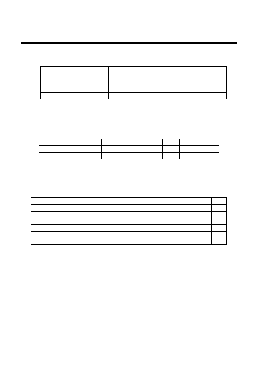
DC Electrical Characteristics
Table 5 DC characteristics (3 V)
(Unless otherwise specified : Ta
=25∞C, V
DD
=3 V, DS-VT-200 (crystal oscillator, C
L
=6 pF, 32,768 Hz) manufactured by SII Quartz Techno Ltd.)
Item Symbol
Applicable
pin Condition Min.
Typ.
Max.
Unit
Operating voltage range
V
DD
-
Ta
= -20 to +70∞C 1.3
3.0
3.6
V
Current consumption 1
I
DD1
-
During no communications
- 0.55
0.85
µA
Current consumption 2
I
DD2
-
During communications
(SCK
=100 kHz)
- 12 20 µA
Input leak current 1
I
IZH
SCL,
SDA
V
IN
=V
DD
-0.5
- 0.5 µA
Input leak current 2
I
IZL
SCL,
SDA
V
IN
=V
SS
-0.5
- 0.5 µA
Output leak current1
I
OZH
INT1, INT2 SDA
V
OUT
=V
DD
-0.5
- 0.5 µA
Output leak current2
I
OZL
INT1, INT2 SDA
V
OUT
=V
SS
-0.5
- 0.5 µA
Input voltage 1
V
IH
SDA,
SCL
- 0.8◊V
DD
-
- V
Input voltage 2
V
IL
SDA, SCL,
-
-
- 0.2◊V
DD
V
Output current 1
I
OL1
INT1,
INT2
V
OUT
=0.4 V
1.5
2.5
- mA
Output current 2
I
OL2
SDA
V
OUT
=0.4 V
5
10
- mA
Power voltage detection
voltage 1
V
DET1
-
Ta
=+25∞C
- 1.45 - V
Power voltage detection
voltage 2
V
DET2
-
Ta
= -20 to +70∞C 1.15
- 1.65 V
REAL-TIME CLOCK
S-35L32A
Rev.1.3
_00
8
Seiko Instruments Inc.
AC Electrical Characteristics
Table 6 Measurement conditions
Input pulse voltage
0.1
◊V
DD
to 0.9
◊V
DD
Input pulse
rising/falling time
20 ns
Output judgement
voltage
0.5
◊V
DD
Output load
100 pF
+pull-up resistance 1.0 k
V
DD
R=1.0 k
SDA
C
=100 pF
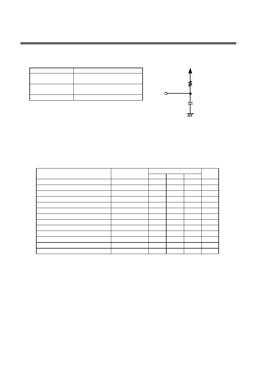
Caution Both IC and load powers are
the same V
DD
Figure 4 Output load circut
Table 7 AC properties
V
DD
=1.7 V to 5.5 V
Item Symbol
Min. Typ. Max.
Unit
SCL clock frequency
f
SCL
0
-
100
kHz
SCL clock "L" time
t
LOW
4.7
-
-
µs
SCL clock "H" time
t
HIGH
4.0
-
-
µs
SDA output delay time
t
PD
-
-
3.5
µs
Start condition setup time
t
SU
, t
STA
4.7
-
-
µs
Start condition holding time
t
HD
, t
STA
4.0
-
-
µs
Data input setup time
t
SU
, t
DAT
250
-
-
ns
Data input holding time
t
HD
, t
DAT
150
-
-
ns
Stop condition setup time
t
SU
, t
STO
4.7
-
-
µs
SCL, SDA rising time
t
R
-
-
1.0
µs
SCL, SDA falling time
t
F
-
-
0.3
µs
Bus release time
t
BUF
4.7
-
-
µs
Noise suppression time
t
I
-
-
100
ns
REAL-TIME
CLOCK
Rev.1.3
_00
S-35L32A
Seiko
Instruments
Inc.
9
SCL
SDA IN
SDA OUT
t
BUF
t
R
t
SU
, t
STO
t
SU
, t
DAT
t
HD
, t
DAT
t
DH
t
PD
t
HIGH
t
LOW
t
HD
, t
STA
t
SU
, t
STA
t
F
Figure 5 Bus timing
REAL-TIME CLOCK
S-35L32A
Rev.1.3
_00
10
Seiko Instruments Inc.
Description of Operation
1. Serial
interface
S-35L32A receives various commands through the I
2
C-BUS-based serial interface to read/write data. The
method of I
2
C-BUS-based transfer is described here.
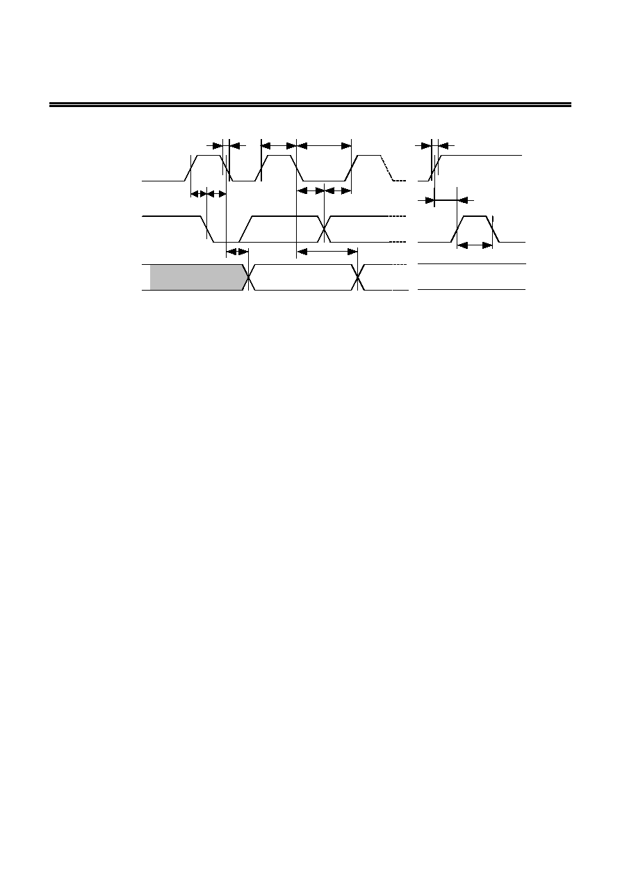
1.1 Start condition
Changing the SDA line from "H" to "L" when the SCL line is "H" activates the start condition.
All the operations begin at the start condition.
1.2 Stop condition
Changing the SDA line from "L" to "H" when the SCL line is "H" activates the stop condition.
During a read sequence, any read operation is stopped and a device enters its stand-by mode when
a stop condition is received.
t
SU.
t
STA
t
HD.
t
STA
t
SU.
t
STO
Start condition
Stop condition
SCL
SDA
Figure 6 Start/Stop condition
1.3 Data transfer
When the SDA line is changed while the SCL line is on "L", data transfer is performed.
When the SDA line is changed while the SCL line is on "H", a start or stop condition is recognized.
t
SU,
t
DAT
t
HD,
t
DAT
SCL
SDA
Figure 7 Data transfer timing
REAL-TIME
CLOCK
Rev.1.3
_00
S-35L32A
Seiko
Instruments
Inc.
11
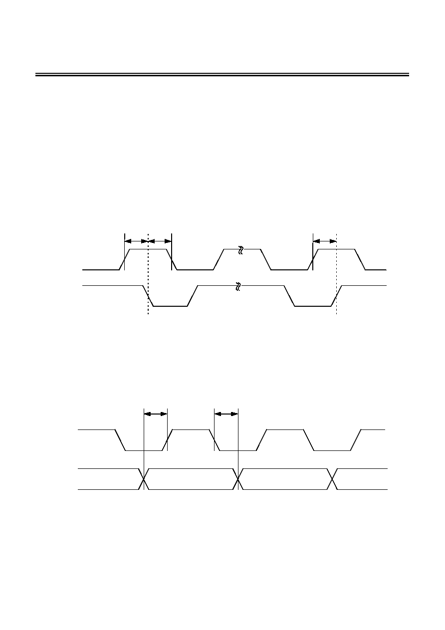
1.4 Acknowledge
Data transfer is performed in 8-bit sequence. A device on the system bus, which succeedingly
receives data during a period of a ninth clock cycle, puts the SDA line on "L" and returns an
acknowledge signal meaning that the data has been received.
Acknowledge
output
1
8
9
t
PD
t
DH
Start condition
SCL
(S-35L32A input)
SDA
(Master output)
SDA
(S-35L32A output)
Figure 8 Acknowledge output timing
REAL-TIME CLOCK
S-35L32A
Rev.1.3
_00
12
Seiko Instruments Inc.
1.5 Device addressing
The master device on the system generates a start condition to its slave device to make
communication. It continuously issues the device address of a 4-bit length, the command of a 3-bit
length and the read/write command of a 1-bit length over the SDA bus.
The upper four bits, called a device code, represent a device address and are fixed at "0110".
Command
0
1
1
0
C2
C1
C0
R/W
Device code
MSB
LSB
Read/Write bit
Figure 9 Communication data
1.6 Command configuration
There are eight commands by which the read/write operation of various registers is performed. The
table below lists them.
Table 8 Command list
C2
C1
C0
Description
Number of ACK
0
0
0
Reset (00 (year), 01 (month), 01 (day), 0 (day of week),
00 (minute), 00 (second))
*1
1
0 0 1
Status
register
access
2
0
1
0
Real-time data access 1 (year data to)
8
0
1
1
Real-time data access 2 (hour data to)
4
1
0
0
Alarm time/frequency duty setting 1 (for INT1 pin)
3
1
0
1
Alarm time/frequency duty setting 2 (for INT2 pin)
3
1 1 0
Test
mode
start
*2
1
1 1 1
Test
mode
end
*2
1
*1. Don't care the R/W bit of this command.
*2. This command is access-disabled due to specific use for the IC test.
REAL-TIME
CLOCK
Rev.1.3
_00
S-35L32A
Seiko
Instruments
Inc.
13
1.7 Data reading
After a start condition is detected from the outside, the device code and command are received. At
this point, the real-time reading mode or status register reading mode is entered when the read/write bit
is "1". In either the real-time reading mode or status register reading mode, data are output in the order
from LSB.
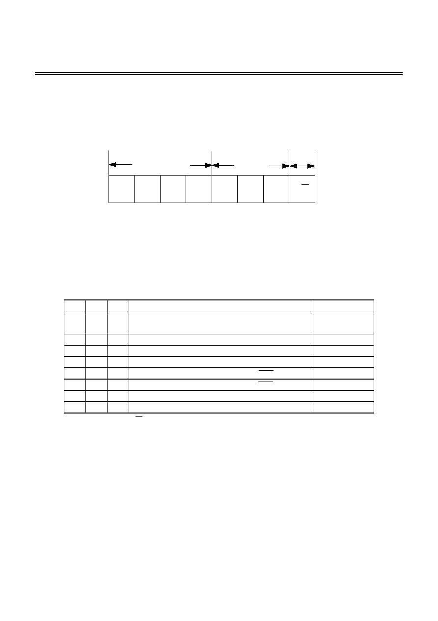
(1) Real-time data reading 1
Command
S
T
A
R
T
0
1
1
0
R
E
A
D
S
T
O
P
DEVICE
ADDRESS
R
/
W
M
S
B
SDA LINE
0
1
0
A
C
K
L
S
B
A
C
K
1
Real-time data
access 1 command
Year data
L
S
B
M
S
B
L
S
B
M
S
B
Second data
A
C
K
NO ACK from
Master Device
(2) Real-time data reading 2
S
T
A
R
T
0 1 1 0
R
E
A
D
S
T
O
P
DEVICE
ADDRESS
R
/
W
M
S
B
SDA LINE
0
1 1
A
C
K
L
S
B
A
C
K
1
Command
Real-time data
access 2 command
Hour data
L
S
B
M
S
B
L
S
B
M
S
B
Second data
A
C
K
NO ACK from
Master Device
(3) Status register reading
S
T
A
R
T
0 1 1 0
R
E
A
D
DEVICE
ADDRESS
R
/
W
M
S
B
SDA LINE
0
1
A
C
K
L
S
B
1
Command
Status register
access command
Status data
L
S
B
M
S
B
0
S
T
O
P
NO ACK from
Master Device
Figure 10 Read communication
Caution
ACK Upside:
Generate from the master device
ACK Downside: Generate from the S-35L32A
REAL-TIME CLOCK
S-35L32A
Rev.1.3
_00
14
Seiko Instruments Inc.
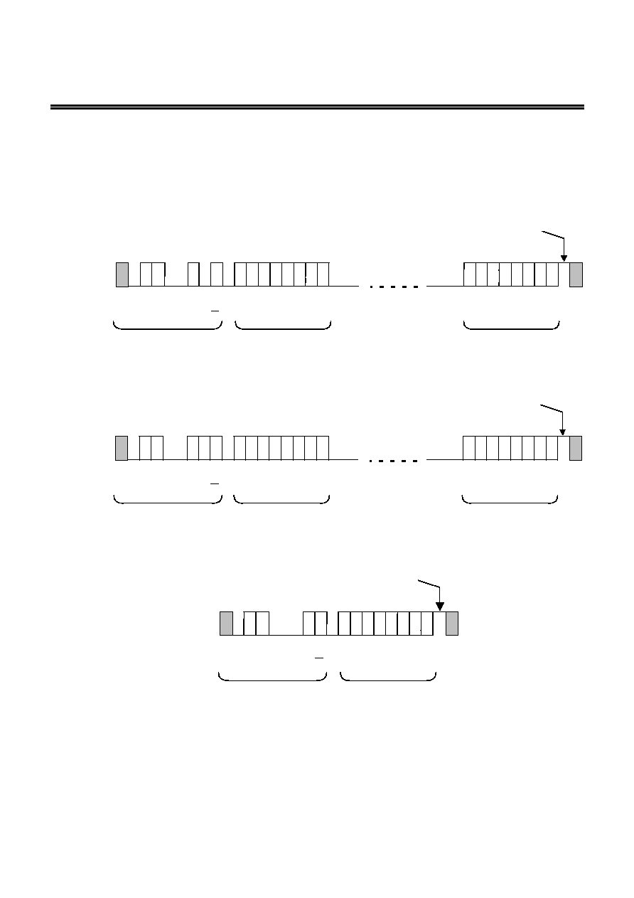
1.8 Data writing
After a start condition is detected from the outside, the device code and command are received. At
this point, the real-time-data-writing mode or other register-writing mode is entered when the read/write
bit is "0". Data must be entered in the order from LSB of the real-time data writing mode or status
register-writing mode. In real-time data writing, the counter of a calendar and time is reset when the
ACK signal rises following the real-time writing command, and any update operation is disabled. After a
minute data is received, the end of a month is corrected while a second data is imported. Then, the
count-up is started when the ACK signal rises after the second data is received.
(1) Real-time data writing 1
S
T
A
R
T
0 1 1 0
W
R
I
T
E
S
T
O
P
DEVICE
ADDRESS
R
/
W
M
S
B
SDA LINE
0
1 0
A
C
K
L
S
B
A
C
K
A
C
K
0
Command
Real-time data
access 1 command
Year data
L
S
B
M
S
B
L
S
B
M
S
B
Second data
(2) Real-time data writing 2
S
T
A
R
T
0 1 1 0
S
T
O
P
DEVICE
ADDRESS
R
/
W
M
S
B
SDA LINE
0
1 1
A
C
K
L
S
B
A
C
K
A
C
K
0
Command
Real-time data
access 2 command
Hour data
L
S
B
M
S
B
L
S
B
M
S
B
Second data
W
R
I
T
E
(3) Status register writing
S
T
A
R
T
0 1 1 0
DEVICE
ADDRESS
R
/
W
M
S
B
SDA LINE
0
1
A
C
K
L
S
B
A
C
K
0
Command
Status register
access command
Status data
L
S
B
M
S
B
0
S
T
O
P
W
R
I
T
E
Figure 11 Write communication
REAL-TIME
CLOCK
Rev.1.3
_00
S-35L32A
Seiko
Instruments
Inc.
15
2. Register configuration
2.1 Real-time data register
The real-time data register is a 56-bit register which stores the BCD code of the data of year, month,
day, day of week, hour, minute and second. Any read/write operation performed by the real-time data
access command sends or receives the data from LSB on the first digit of the year data.
Y80 Y40 Y20 Y10 Y8
Y4
Y2
Y1
MSB
LSB
Year data (00 to 99)
YF
0
0
M10 M8
M4
M2
M1
MSB
LSB
Month data (01 to 12)
Sets the lower two digits of the year (00 to 99)
and links together with the auto calendar feature
until 2,099.
The count value is automatically changed by the
auto calender feature:
1, 3, 5, 7, 8, 10, 12: 1 to 31
4, 6, 9, 11: 1 to 30
2 (leap year): 1 to 29
2 (common year): 1 to 28
AM/
PM
0
0
D20 D10 D8
D4
D2
D1
MSB
LSB
Day data (01 to 31)
0
0
0
0
0
W4
W2
W1
MSB
LSB
Day of week data (00 to 06)
A septenary counter. Set it so that it
corresponds to the day of the week.
0
H20 H10 H8
H4
H2
H1
MSB
LSB
Hour data (00 to 23 or 00 to 11)
0
MSB
LSB
Minute data (00 to 59)
TEST S40 S20 S10 S8
S4
S2
S1
MSB
LSB
Second data (00 to 59) and test flag
m10 m8
m4
m2
m1
AM/PM : For 12-hour expression, 0:AM and 1:PM.
For 24-hour expression, this flag has no
meaning but either 0 or 1 must be written.
TEST : Turns to "1" during the test mode.
m20
m40
Year Flag (YF)
The count value is set to 0 when changing date from 59:
59:23, Dec. 31, 1999 to 00: 00:00, Jan. 1, 2000. At
reset, it is set to 1. Set the year data to 0 for 2000s and
for 1900s because it is not automatically set or reset.
Figure 12

REAL-TIME CLOCK
S-35L32A
Rev.1.3
_00
16
Seiko Instruments Inc.
2.2 Status
register
The status register is an 8-bit register of which allows you to display and set various modes. The
POWER flag is read-only and others are read/write-enabled.
B7
LSB
POWER
12/24
R
R/W
R/W
R/W
R/W
R/W
R/W
R/W
INT1AE
INT2AE
INT2ME
INT1ME
MSB
B6
B5
B4
B3
B2
B1
B0
INT2FE
INT1FE
Figure 13
B7:POWER
This flag turns to "1" if the power voltage detecting circuit operates during power-
on or changes in power voltage (below V
DET
). Once turning to "1", this flag does
not turns back to "0" even when the power voltage reaches or exceeds the
detection voltage. When the flag is "1", you must send the reset command (or
status register read command) and turn it to "0". It is a read-only flag.
B6:12/24
This flag is used to set 12-hour or 24-hour expression.
0 : 12-hour expression
1 : 24-hour expression
B5:INT1AE, B4:INT2AE
This flag is used to choose the state of INT1 pin (or INT2 pin) output with alarm
interrupt output set. Enable this flag after setting alarm time that forms a meeting
condition in the INT1 register (or INT2 register):
0 : Alarm interrupt output is disabled.
1 : Alarm interrupt output is enabled.
B3:INT1ME, B2:INT2ME
This flag is used to make the output of the INT1 pin (or INT2 pin) per-minute edge
interrupt or per-minute steady interrupt. To make the output per-minute steady
interrupt, set "1" at INT1ME and INT1FE (or INT2ME and INT2FE).
0 : Alarm interrupt or selected frequency steady interrupt output
1 : Per-minute edge interrupt or per-minute steady interrupt output
B1:INT1FE, B0:INT2FE
This flag is used to make the output of the INT1 pin (or INT2 pin) per-minute
steady interrupt output (a period of one minute, 50% of duty) or selected
frequency steady interrupt. Note that the INT1 register (INT2 register) is
considered as the data of frequency/duty if selected frequency steady interrupt is
chosen.
0 : Alarm interrupt or per-minute edge interrupt output
1 : Per-minute steady interrupt or selected frequency steady
interrupt output
REAL-TIME
CLOCK
Rev.1.3
_00
S-35L32A
Seiko
Instruments
Inc.
17
2.3 Alarm time/Frequency duty setting register
There are two types of alarm time/frequency duty setting registers, 16-bit registers, which set alarm
time or frequency duty. They are switched by INTxAE or INTxFE register. AM/PM flag to be set must be
in accordance with 12-hour or 24-hour expression. If AM/PM flag is not rightly then set hour data is not
met to alarm data. The alarm time/frequency duty setting register is a write-only register.
(1) When INTxAE
=
=
=
= 1
AM/
PM
0
H8
H4
H2
H1
MSB
LSB
0
m8
m4
m2
m1
MSB
LSB
H20
H10
m10
m20
m40
INT1 register
AM/
PM
0
H8
H4
H2
H1
MSB
LSB
0
m8
m4
m2
m1
MSB
LSB
H20
H10
m10
m20
m40
INT2 register
Figure 14 INT1 register (alarm)
Figure 15 INT2 register (alarm)
INT1 and INT2 registers are considered as alarm time data. Having the same configuration as the
time and minutes registers of real-time data register configuration, they represent hours and minutes
with BCD codes. When setting them, do not set any none-existent day. Data to be set must be in
accordance with 12-hour or 24-hour expression that is set at the status register.

REAL-TIME CLOCK
S-35L32A
Rev.1.3
_00
18
Seiko Instruments Inc.
(2) When INTxFE
=
=
=
= 1
INT1 and INT2 registers are considered as frequency duty data. By turning each bit of the registers
to "1", a frequency corresponding to each bit is chosen in an ANDed form.
f0
MSB
LSB
INT1 register
MSB
LSB
f1
f2
f3
f4
f5
f6
f7
f8
f9
f10
f11
f12
f13
f14
f15
f0
MSB
LSB
INT2 register
MSB
LSB
f1
f2
f3
f4
f5
f6
f7
f8
f9
f10
f11
f12
f13
f14
f15
f0 32768
Hz f4 2048
Hz f8 128
Hz f12 8
Hz
f1 16384
Hz f5 1024
Hz f9 64
Hz f13 4
Hz
f2 8192
Hz f6 512
Hz f10 32
Hz f14 2
Hz
f3 4096
Hz f7 256
Hz f11 16
Hz f15 1
Hz
Figure 16 INT1 and INT2 registers (frequency/duty)
REAL-TIME
CLOCK
Rev.1.3
_00
S-35L32A
Seiko
Instruments
Inc.
19
32 kHz
Example
If f15 to f0
= 000A H
16 kHz
8 kHz
4 kHz
2 kHz
Set to selected frequency steady
interrupt output
INT1 or INT2
terminal output
Figure 17 Clock output
2.4 Test flag
The test flag is a 1-bit register to which assigned MSB of the second data of the real-time data
register. If a transferred data is considered as the test mode starting command due to the receiving of
the test mode starting command or noises, "1" is set. When "1" is set, you must send the test mode
ending command or reset command.
3. Initialization
Note that S-35L32A has different initializing operations, depending on states.
3.1 When power
is turned on
When power is turned on, the status register is set to "82h" and the INT1 register to "8000h" by the
power-on detecting circuit. In other words, "1" is set at the bit 7 (POWER flag) of the status register and
the clock of 1 Hz is output from the INT1 pin. This is provided to adjust oscillating frequencies. In
normal use, the reset command must be sent when power is turned on.
Real-time data register : 00 (year), 01 (month), 01 (day), 0 (day of week), 00 (hour), 00
(minute), 00 (second) (year flag: "1")
Status register
: "82h"
INT1 register
: "8000h"
INT2 register
: "0000h"
3.2 When the power voltage detecting circuits operates
The power voltage detecting circuit included in S-35L32A operates and sets "1" at the bit 7 (POWER
flag) of the internal status register when power is turned on or power voltage is reduced. Once "1" is set,
it is held even after the power voltage gets equal to or higher than the detection voltage, i.e., power
voltage detector threshold. When the flag has "1", you must send the reset command from CPU and
initialize the flag. At this point, other registers do not change, however, if the POWER flag has "0" during
the power-on reset of CPU (S-35L32A does not reach any indefinite area during backup), you do not
have to send the reset command.

REAL-TIME CLOCK
S-35L32A
Rev.1.3
_00
20
Seiko Instruments Inc.
3.3 When the reset command is received
When the reset command is received, each register turns as follows:
Real-time data register : 00 (year), 01 (month), 01 (day), 0 (day of week), 00 (hour), 00
(minute), 00 (second) (year flag : "1")
Status register
: "00h"
INT1 register
: "0000h"
INT2 register
: "000h"
0
1
1
0
DEVICE
ADDRESS
R
/
W
M
S
B
SDA LINE
0
0
1
A
C
K
L
S
B
1
command
status access command
V
DD
POWER
flag
0
1
1
0
DEVICE
ADDRESS
R
/
W
M
S
B
SDA
LINE
0
0
1
A
C
K
L
S
B
1
command
status access command
V
DD
POWER
flag
0
1
1
0
DEVICE
ADDRESS
R
/
W
M
S
B
0
0
A
C
K
L
S
B
command
1
1
0
1
0
0
0
0
A
C
K
S
T
O
P
S
T
A
R
T
0
POWER flag
0
Don't care
backup state (S-35L32A does not reach any indefinite
S
T
A
R
T
0
1
1
0
R
/
W
M
S
B
0
1
A
C
K
L
S
B
1
0
0
0
0
0
0
0
A
C
K
S
T
O
P
0
POWER flag
0
S
T
A
R
T
S
T
A
R
T
S
T
O
P
L
S
B
real-time data access
CPU down
reset command
status data
1
status data
DEVICE
ADDRESS
command
1
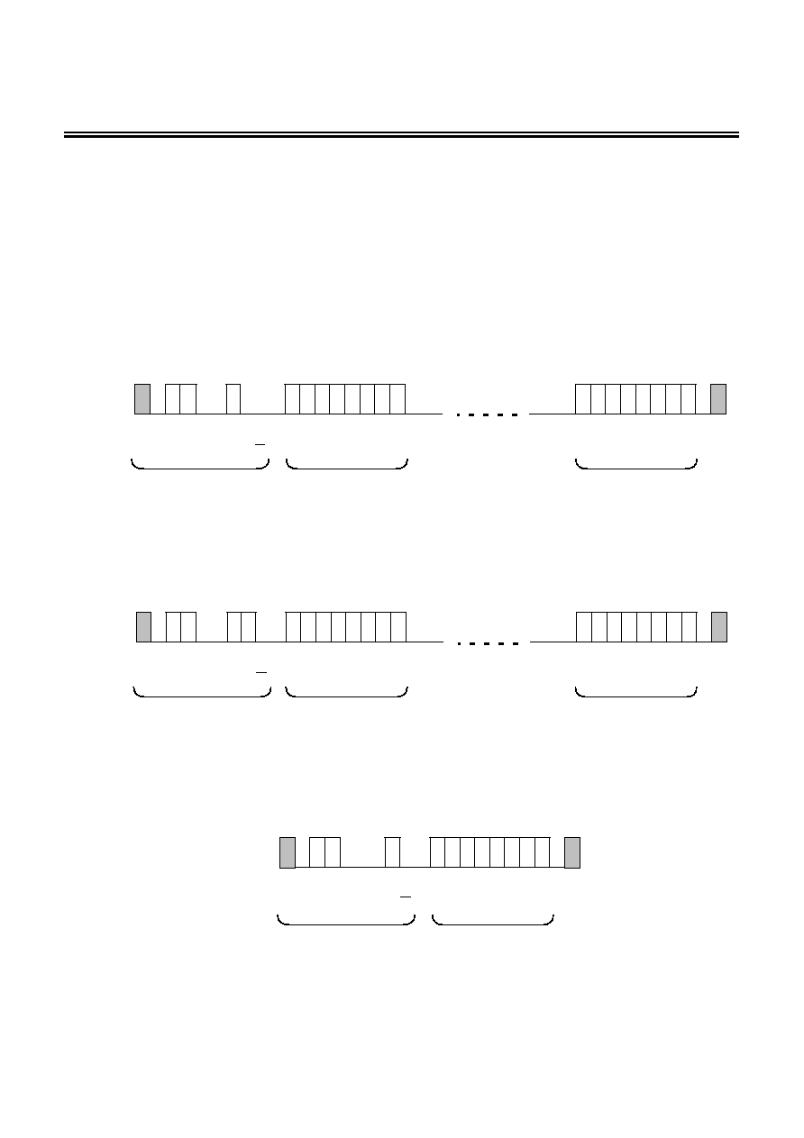
Figure 18 Initializing
REAL-TIME
CLOCK
Rev.1.3
_00
S-35L32A
Seiko
Instruments
Inc.
21
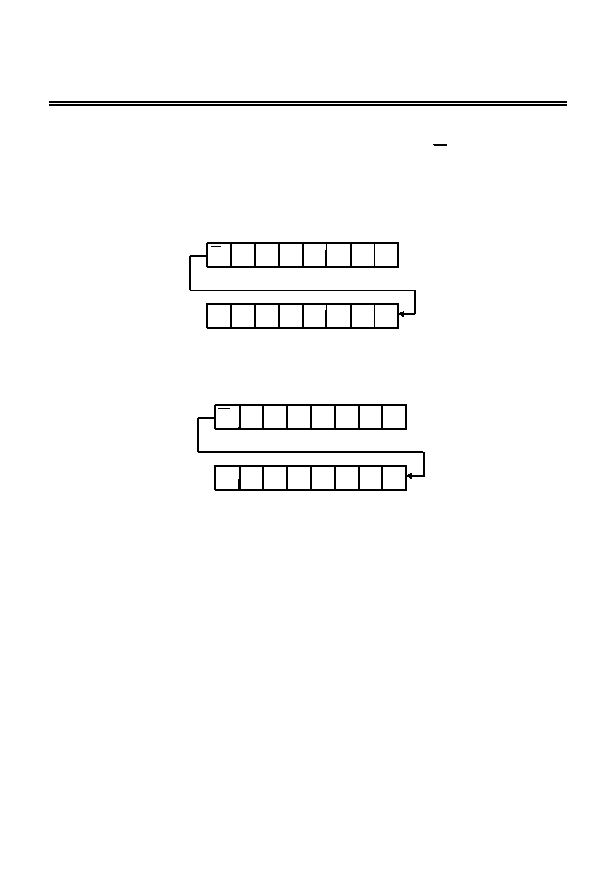
4. Processing of none-existent data and end-of-month
When writing real-time data, validate it and treat any invalid data and end-of-month correction.
[None-existent data processing]
Table 9
Register Normal
data
Error
data
Result
Year data
00 to 99
XA to XF, AX to FX
00
Month data
01 to 12
00, 13 to 19, XA to XF
01
Day data
01 to 31
00, 32 to 39, XA to XF
01
Day of week data
0 to 6
7
0
Hour data
*1
(24-hour)
(12-hour)
0 to 23
0 to 11
24 to 29, 3X, XA to XF
12 to 19, XA to XF
00
00
Minute data
00 to 59
60 to 79, XA to XF
00
Second data
*2
00 to 59
60 to 79, XA to XF
00
*1.
For 12-hour expression, write the AM/PM flag.
The AM/PM flag is ignored in 24-hour expression, but "0" for 0 to 11 o'clock and "1" for 12 to
23 o'clock are read in a read operation.
*2.
None-existent data processing for second data is performed by a carry pulse one second
after the end of writing. At this point, the carry pulse is sent to the minute counter.
[End-of-month correction]
Any none-existent day is corrected to the first day of the next month. For example, February 30 is
changed to March 1. Leap-year correction is also performed here.

REAL-TIME CLOCK
S-35L32A
Rev.1.3
_00
22
Seiko Instruments Inc.
5. Interrupt
There are different five output formats from the INT1 and INT2 pin, which are chosen by the INTxAE,
INTxME and INTxFE bits of the status register (x: 1 or 2).
(1) Alarm interrupt output
Alarm interrupt is enabled by setting hour and minute data to the INT1 register (or INT2 register)
and turning the status register's INT1AE to "1" and INT1ME and INT1FE to "0" (or INT2AE to "1" and
INT2ME and INT2FE to "0"). When set hour data is met, "K" is output from the INT1 pin (or INT2 pin).
Since the output is held, rewrite INT1AE (or INT2AE) of the status register to "0" through serial
communication to turn the output to high (OFF state).
The coincidence signal is set when minute changes from 59 seconds to 0 second and outputs the
"L" signal from the INT1 pin (or INT2 pin). When you perform disable or enable communication within
the coincidence period (1 minute), pay attention that INT1 pin (or INT2 pin) remains "H" level (OFF
state).
(2) Selected frequency steady interrupt output
When you set frequency/duty data to the INT1 register (or INT2 register) and turn the status
register's INT1ME to "0" and INT1FE to "1" (or INT2ME to "0" and INT2FE to "1"), clock set at the INT1
register (or INT2 register) is output from the INT1 pin (or INT2 pin).
(3) Per-minute edge interrupt output
When a first minute carry is performed after the status register's INT1ME is set with "1" and INT1FE
with "0" (or INT2ME with "1" and INT2FE with "0"), "L" is output from the INT1 pin (or INT2 pin). Since
the output is held, rewrite INT1AE, INT1ME and INT1FE (or INT2AE, INT1ME and INT2FE) of the
status register to "0" through serial communication to turn the output to high (OFF state). When you
perform disable or enable communication while the minute carry processing signal is being retained
(for 123
µs), "L" signal is output from the INT1 pin (or INT2 pin) again.
(4) Per-minute steady interrupt output
When a first minute carry is performed after the status register's INT1ME and INT1FE are set with
"1" (or INT2ME and INT2FE with "1"), clock is output from the INT1 pin (or INT2 pin) with a period of
one minute (50% duty).
When you perform disable or enable communication while the INT1 pin (or INT2 pin) is at "L," "L"
signal is output from the INT1 pin (or INT2 pin) again.
Caution 1. If changing an output mode, give care to the state of the INT1and INT2 registers and
output.
2. If per-minute-edge-interrupt-output or per-minute-steady-interrupt-output is chosen, the
INT1 and INT2 registers have no meaning.
REAL-TIME
CLOCK
Rev.1.3
_00
S-35L32A
Seiko
Instruments
Inc.
23
Table 10 Interrupt description
NO. INT1AE INT1ME INT1FE
Description
0
0
0
0
INT1 pin output disabled (No interrupt output)
1
*
0
1
Selected frequency steady interrupt output from the
INT1 pin
2
*
1
0
Per-minute edge interrupt output from the INT1 pin
3
*
1
1
Per-minute steady interrupt output from INT1 pin
4
1
0
0
Alarm interrupt output from INT1 pin
NO. INT2AE INT2ME INT2FE
Description
5
0
0
0
INT2 pin output disabled (No interrupt output)
6
*
0
1
Selected frequency steady interrupt output from the
INT2 pin
7
*
1
0
Per-minute edge interrupt output from the INT2 pin
8
*
1
1
Per-minute steady interrupt output from INT2 pin
9
1
0
0
Alarm interrupt output from INT2 pin
Note * Don't care (both 0 and 1 are available)
REAL-TIME CLOCK
S-35L32A
Rev.1.3
_00
24
Seiko Instruments Inc.
(1)
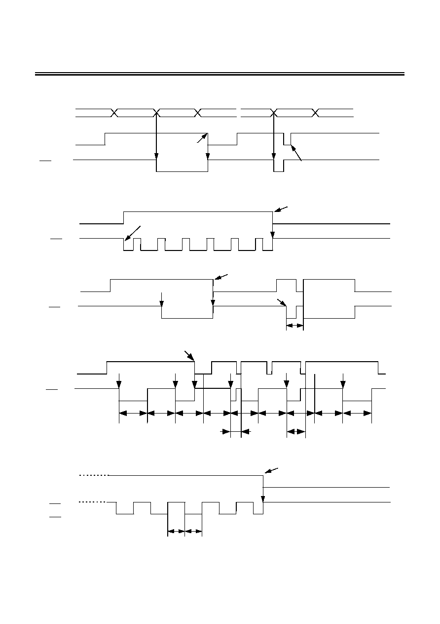
Alarm interrupt output
hour
minute
INTxAE
INTx pin
INTxME
=INTxFE=0
OFF
Once the alarm time is reset, no "L" signal
generates even when you enable it within the
conincidence time.
Alarm time corresponds
Alarm time corresponds
Change by program
h (n-2)
h (n-1)
h (n)
h (n+1)
K (m-1)
K (m)
K (m+1)
(2) Selected frequency steady interrupt output
INTxFE
INTx pin
INTxAE
=INTxME=0
Free run output starts
Change by program
OFF
(3) Per-minute edge interrupt output
INTxME
INTx pin
INTxAE
=INTxFE=0
OFF
Minute-carry processing
Change by program
"L" signal is output again in case of
123
µs or less
Minute-carry processing
(4) Per-minute steady interrupt output
INTxFE,INTxME
INTx pin
INTxAE
=0
Minute-carry
processing
Minute-carry
processing
Change by program (OFF)
30 s
30 s
30 s
30 s
30 s
30 s
30 s
Minute-carry
processing
Minute-carry
processing
30 s
Minute-carry
processing
"L" signal is output again in case of 123
µs or less.
"H" signal is output in case of 123
µs or more.
"L" signal is output by the next minute-carry processing.
30 s
(5) During power-on detecting circuit operation
INTxFE
INT2 pin is in
OFF state
INT1 pin
INTxAE
=INTxME=0
Change by the reset command
OFF
0.5 s
0.5 s
Figure 19 Output mode
REAL-TIME
CLOCK
Rev.1.3
_00
S-35L32A
Seiko
Instruments
Inc.
25
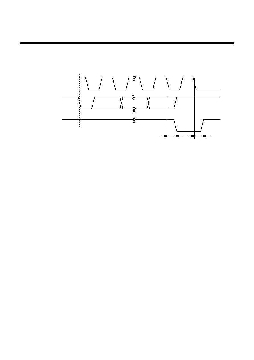
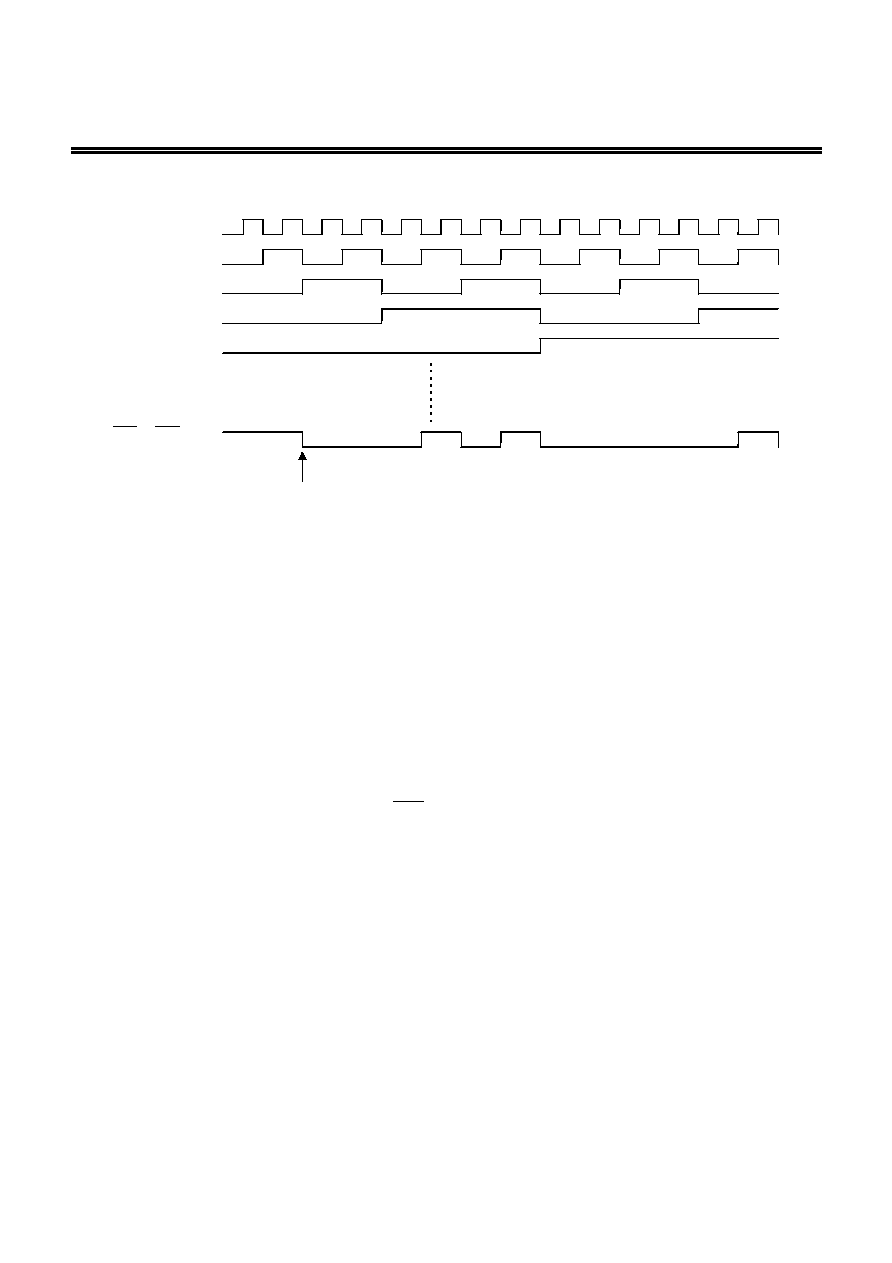
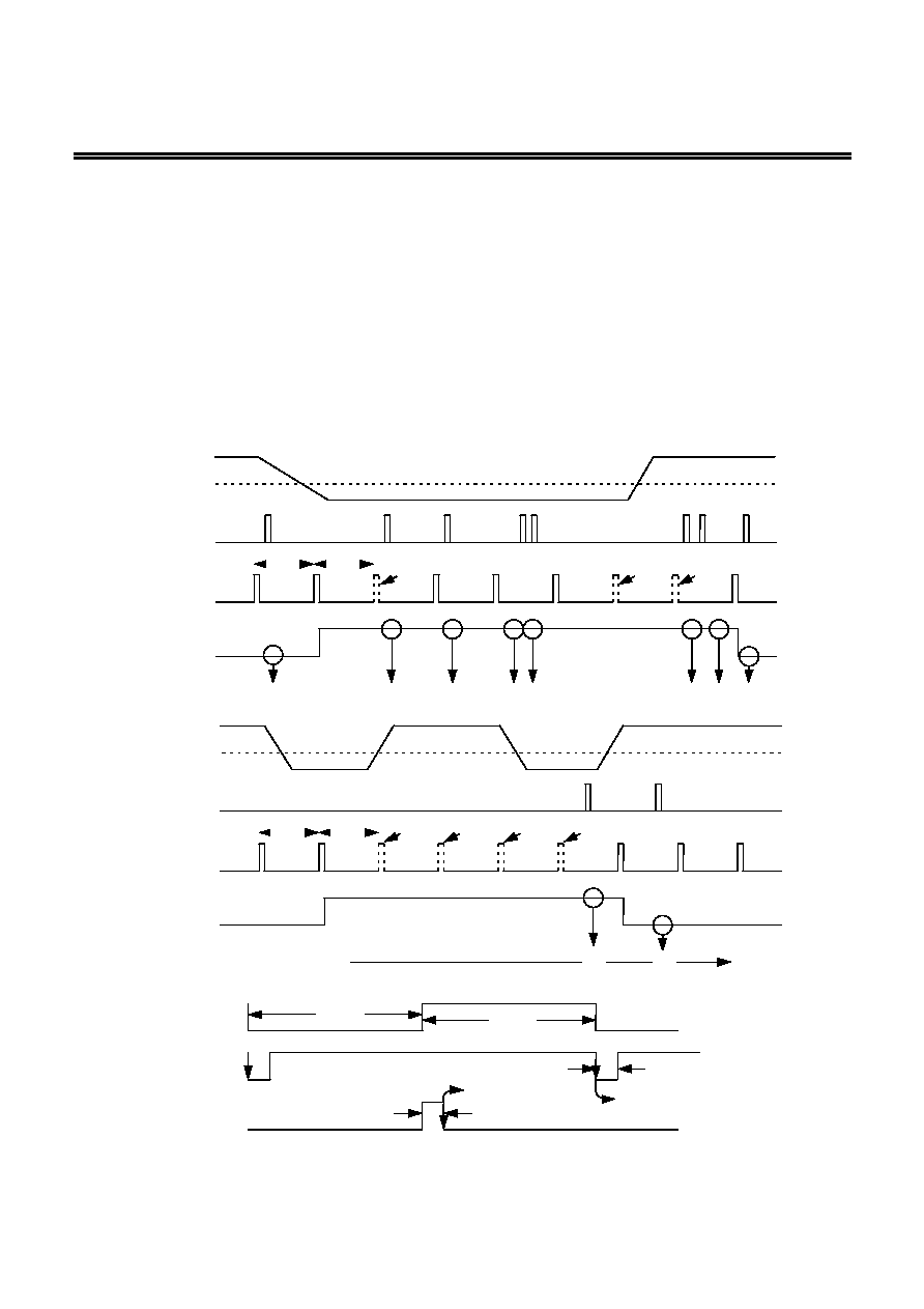
6. Power voltage detecting circuit
S-35L32A has an internal power voltage detecting circuit. This circuit gives sampling movement for only
15.6 ms once a second. If the power voltage decreases below the detection voltage (V
DET
), the BLD latch
circuit latches the "H" level, and sampling movement stops. Only when subsequent communication is of the
status read command, the output of the latch circuit is transferred to the sift register and the sampling
movement is resumed. The decrease in power voltage can be monitored in reading the POWER flag. That is
to say, once it is detected, any detecting operation is not performed and "H" is held unless you perform
initialization or send the status read command.
Caution When power voltage is increased and the first read operation is performed after decrease in
power voltage occurs and the latch circuit latches "H", "1" can be read on the POWER flag,
however, if the next read operation is performed after the sampling of the detecting circuit,
the POWER flag is reset since sampling is subsequently allowed. See the timing diagram
below.
Latch circuit output
Sampling pulse
(0)
1s
1s
Stop
Stop
Stop
(1)
(1)
(1)
(1)
(1)
(1)
(0)
POWER flag
V
DD
V
DET
Communication
Latch circuit
output
Sampling pulse
1 s
1 s
(1)
(0)
Communication
POWER flag
Carry pulse
[Timing of sampling pulse]
0.5 s
0.5 s
7.8 ms
Carry-up timing
1 Hz
15.6 ms
Latch timing
Sampling pulse
(1)
(0)
V
DET
V
DD
Stop
Stop
Stop
Stop
Figure 20 Timing of the power voltage detecting circuit
REAL-TIME CLOCK
S-35L32A
Rev.1.3
_00
26
Seiko Instruments Inc.
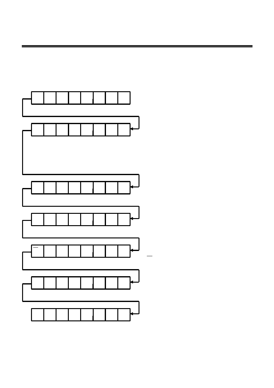
7. Example of software treatment
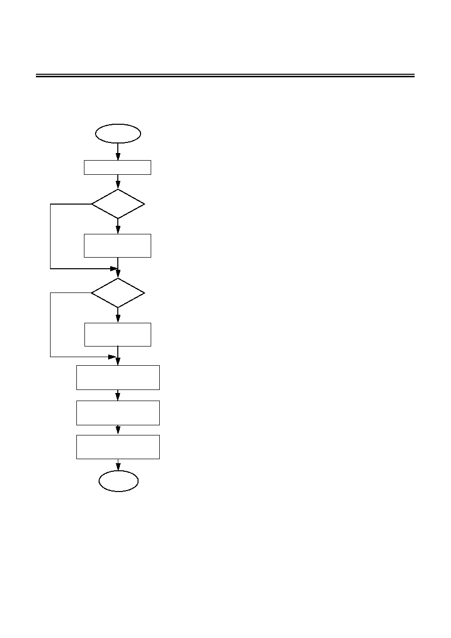
(1) Initialization flow at power-on
NO
YES
START
END
POWER
1
*1.
If S-35L32A is back-up and power is turned on only
on the CPU side, the reset command does not need
transferring.
*2.
If conditions are no good (e.g., noise)
and probable
changes in commands occurs via
serial
communications, it is recommended to
make sure the
TEST
flag.
*3.
The test ending command may be used alternately.
Power on
Reset command
transfer
NO
YES
TEST
=1
Reset command
transfer
Status register setting
command transfer
Real-time data setting
command transfer
INTx register setting
command transfer
*1
*2
*3
Figure 21 Initialization flow
REAL-TIME
CLOCK
Rev.1.3
_00
S-35L32A
Seiko
Instruments
Inc.
27
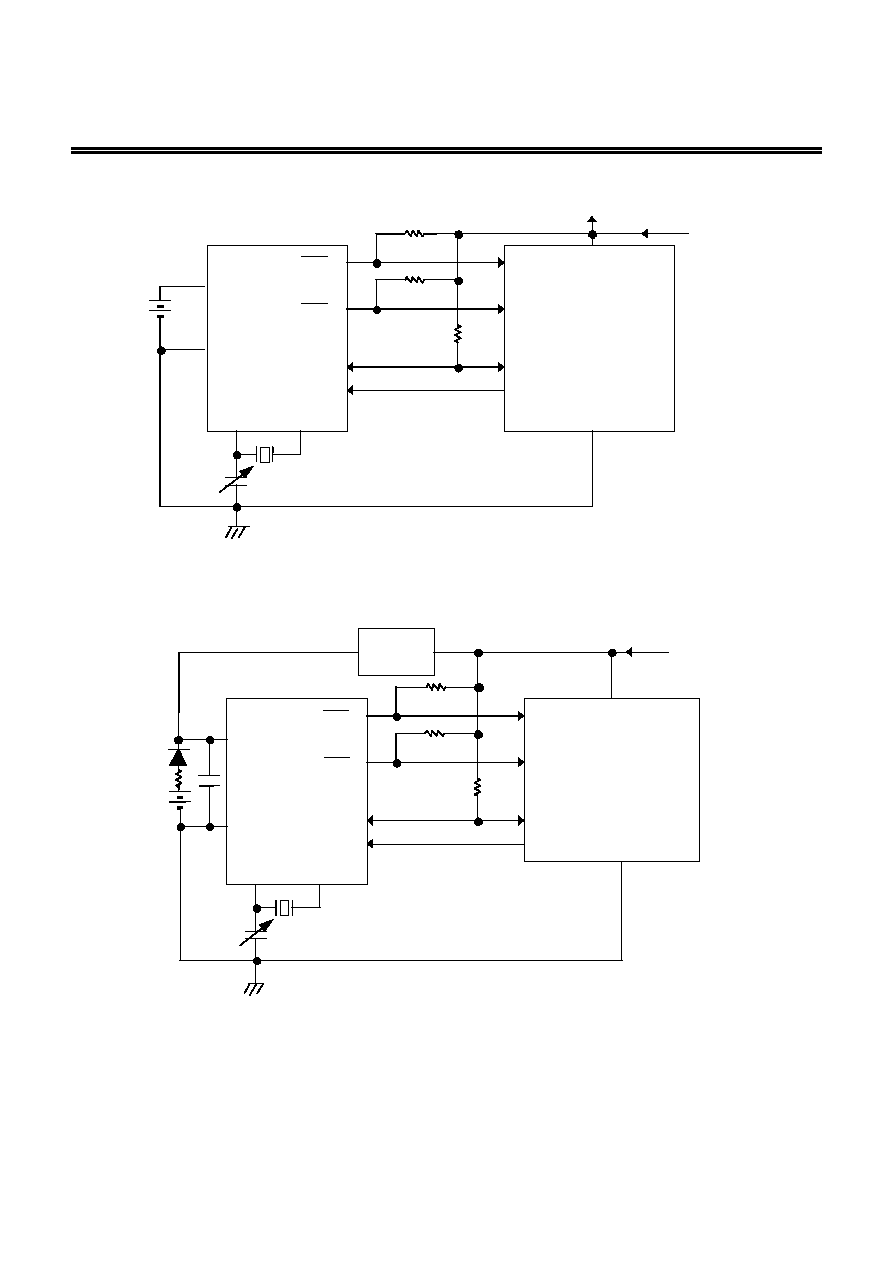
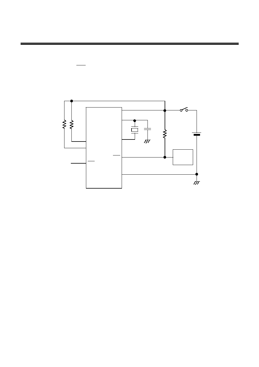
Samples of Application Circuits
Vcc
XOUT
XIN
S-35L32A
SDA
VSS
VDD
SCL
VSS
VCC
External CPU
INT2
INT1
System
power
C
g
Due to the I/O pin with no protective diode on the VDD side, the relation of VCC
VDD has no
problem but give great care to the standard. Make communications after the system power is turned on
and a stable state is obtained.
Figure 22 Application circuit 1
VSS
VCC
External CPU
Power
switching
circuit
XOUT
XIN
S-35L32A
SDA
VSS
VDD
SCL
INT2
INT1
System
power
C
g
Make communications after the system power is turned on and a stable state is obtained.
Figure 23 Application circuit 2
Caution The application circuits above do not guarantee proper operation.
Evaluate in the actual application to determine the correct constants
.
REAL-TIME CLOCK
S-35L32A
Rev.1.3
_00
28
Seiko Instruments Inc.
Adjustment of Oscillating Frequency
1. Configuration of the oscillating circuit
Since crystal oscillation is sensitive to external noises (clock accuracy is affected), the following measures
are essential for optimizing your oscillating circuit configuration:
(1) Place S-35L32A, crystal oscillator and external capacitor (C
g
) as close to each other as possible.
(2) Make high the insulation resistance between pins and the substrate wiring patterns of XIN and XOUT.
(3) Do not place any signal or power lines close to the oscillating circuit.
XIN
XOUT
C
g
S-35L32A
C
d
R
d
R
f
Crystal oscillator:32.768 Hz
C
L
=6 pF
C
g
=3 to 35pF
Oscillating circuit internal constant standard
values:
R
f
=20 M
R
d
=220 k
C
d
=12 pF
Figure 24 Connection diagram
REAL-TIME
CLOCK
Rev.1.3
_00
S-35L32A
Seiko
Instruments
Inc.
29
2. Measurement of oscillating frequencies
When power is turned on, S-35L32A has the internal power-on detecting circuit operating and outputs a
signal of 1 Hz from the INT1 pin to select the crystal oscillator and optimize the C
g
value. Turn power on and
measure the signal with a frequency counter following the circuit configuration shown in Figure 25.
Remark If the error range is
±1 ppm in relation to 1 Hz, time is shifted by approximately 2.6 seconds a
month (as calculated using the following expression)
10
-6
(1ppm)
◊60 seconds ◊60 minutes ◊24 hours ◊ 30 days = 2.592 seconds
Open or
pull-up
Frequency
counter
VDD
XIN
XOUT
SDA
INT2
INT1
VSS
SCL
C
g
S-35L32A
Figure 25 Connection diagram
Caution 1. Use a high-accuracy frequency counter (1 ppm order).
2. Since the 1 Hz signal continues to be output, you must send the reset command in
normal operation.
3. Determine
C
g
with its frequency slow/fast range property referred.
REAL-TIME CLOCK
S-35L32A
Rev.1.3
_00
30
Seiko Instruments Inc.
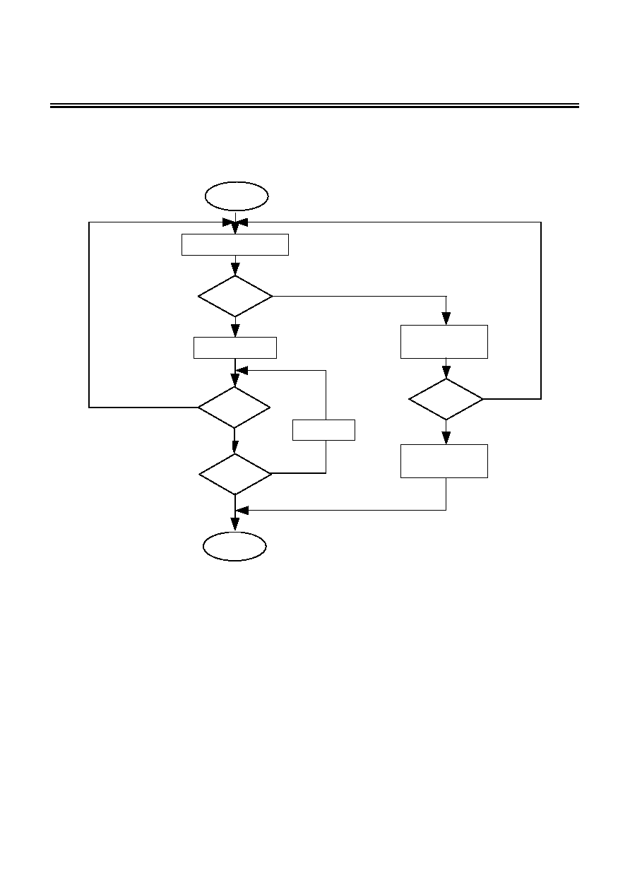
3. Adjustment of oscillating frequencies
Matching of a crystal oscillator with the nominal frequency must be performed with parasitic capacitance
on the board included. Select a crystal oscillator and optimize the C
g
value in accordance with the flow chart
below.
NO
YES
START
Variable
capacity
Select a crystal oscillator.
NO
Is C
g
in the
specification ?
*1
*2
Set C
g
NO
Is it an
optimal
value ?
YES
Change C
g
END
YES
Set to the center of
variable capacitor.
Does
the frequency
match ?
NO
YES
Make fine adjustment
of the frequency in
variable capacity.
*3
*3
<Trimer capacitor>
<Fixed capacitor>
Figure 26 Crystal oscillation setting flow
*1. For making matching adjustment of the IC with a crystal, contact an appropriate crystal maker to
determine the C
L
value (load capacity) and R
I
value (equivalent serial resistance). The C
L
value
= 6 pF
and R
I
value
= 30 k Typ. are recommended values.
*2. C
g
value selection must be performed on the actual PCB since parasitic capacitance affects it. Select the
C
g
value in a range from 3 pF to 35 pF. If the frequency does not match, change the C
L
value of the
crystal.
*3. Adjust the rotation angle of the variable capacity so that the capacity value is somewhat smaller than the
center, and confirm the oscillating frequency and the center value of the variable capacity. This is done
in order to make the capacity of the center value smaller than one half of the actual capacity value
because a smaller capacity value makes a greater quantity of changes in a frequency. If the frequency
does not match, change the C
L
value of the crystal.
Caution 1. Oscillating frequencies are changed by ambient temperature and power voltage. Refer to
property samples.
2. The 32 kHz crystal oscillator operates slower at higher or lower ambient temperature than
20 to 25
∞
∞
∞
∞C. Therefore, it is recommended to adjust or set the oscillator to operate
somewhat faster at normal temperature.

REAL-TIME
CLOCK
Rev.1.3
_00
S-35L32A
Seiko
Instruments
Inc.
31
Precautions
∑ Do not apply an electrostatic discharge to this IC that exceeds the performance ratings of the built-in
electrostatic protection circuit.
∑ SII claims no responsibility for any disputes arising out of or in connection with any infringement by products
including this IC of patents owned by a third party.

REAL-TIME CLOCK
S-35L32A
Rev.1.3
_00
32
Seiko Instruments Inc.
Characteristics (Reference Data)
(1) Standby current vs. C
g
(2) Standby current vs. V
DD
C
g
[pF]
0
10
20
30
C
g
[pF]
0
1
2
3
4
V
DD
[V]
0
0.25
0.5
0.75
1
Ta
=25∞C
I
DD1
[
µA]
V
DD
=3 V
Ta
=25∞C
I
DD1
[
µA]
0
0.25
0.5
0.75
1
1.25
1.5
C
g
=7 pF
(3) Operating current consumption vs. Input clock
(4) Standby current vs. temperature
(5) Oscillating frequency vs. C
g
(6) Oscillating frequency vs. V
DD
V
DD
[V]
0
2
4
6
0
5
10
15
Ta
=25∞C
-4
-2
0
2
4
f/f
[ppm]
Ta
=25∞C
f/f
[ppm]
-40
-20
0
20
40
60
V
DD
=3 V
SCK frequency
[kHz]
0
400
1,000
Ta [
∞C]
-40
0
40
80
Ta
=25∞C
0
10
20
30
40
50
I
DD2
[
µA]
V
DD
=3 V
0
0.25
0.5
0.75
1
V
DD
=3 V, C
g
=7 pF
I
DD1
[
µA]
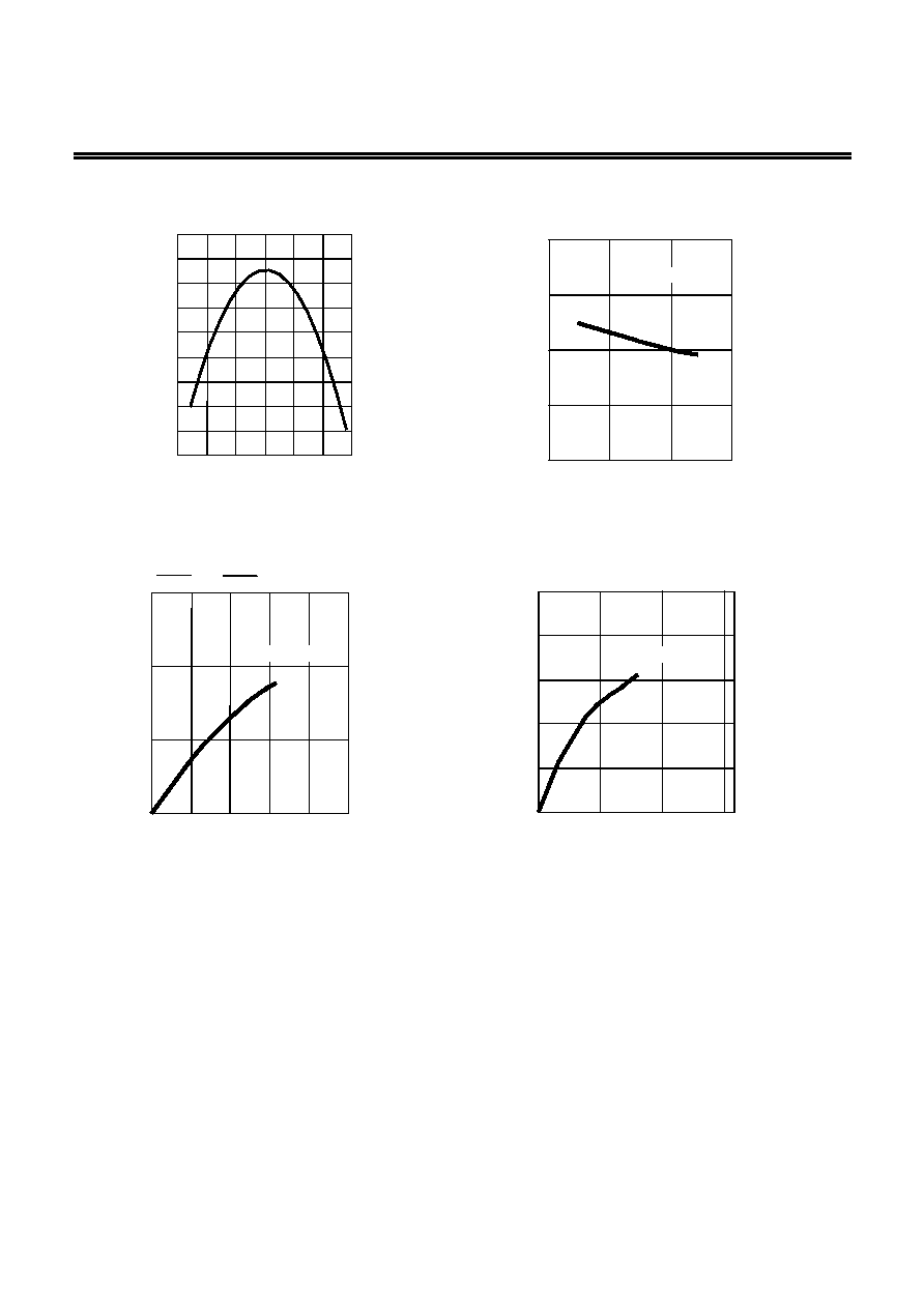
REAL-TIME
CLOCK
Rev.1.3
_00
S-35L32A
Seiko
Instruments
Inc.
33
(8) Oscillation start time vs. C
g
Ta
=25∞C
(9) Output current 1 (V
OUT
vs. I
OL1
)
(7) Oscillating frequency vs. temperature
(10) Output current 2 (V
OUT
vs. I
OL2
)
C
g
[pF]
T
STA
[ms]
0
5
10
15
0
100
200
300
400
V
DD
=3 V
INT1 and INT2 pin, Ta
=25∞C
SIO pin, Ta
=25∞C
V
OUT
[V]
0
0.5
1
1.5
2
2.5
0
5
10
15
0
1
2
3
0
10
20
30
40
50
I
OL1
[mA]
V
DD
=3 V
V
DD
=3 V
V
OUT
[V]
I
OL2
[mA]
f/f
[ppm]
-50
0
50
100
-160
-120
-80
-40
20
Ta
=25∞C, V
DD
=3 V
Ta [
∞C]
No.
TITLE
SCALE
UNIT
mm
0.2±0.1
0.50
3.1±0.3
10
0.15
+0.1
-0.05
6
5
1
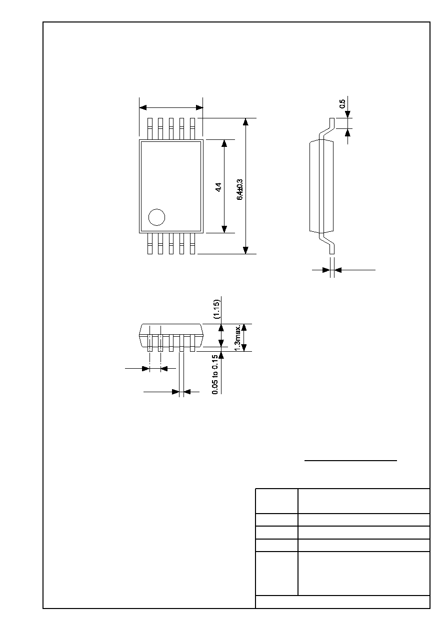
SSOP10-A-PKG Dimensions
Seiko Instruments Inc.
No. FS010-A-P-SD-1.1
FS010-A-P-SD-1.1

1
10
5
6
6.9±0.1
No.
TITLE
SCALE
UNIT
mm
8.0±0.1
1.55±0.05
1.4±0.1
(4.0)
1.55±0.05
4.0±0.1
2.0±0.05
0.3±0.05
Seiko Instruments Inc.
Feed direction
SSOP10-A-Carrier Tape
No. FS010-A-C-SD-1.1
FS010-A-C-SD-1.1
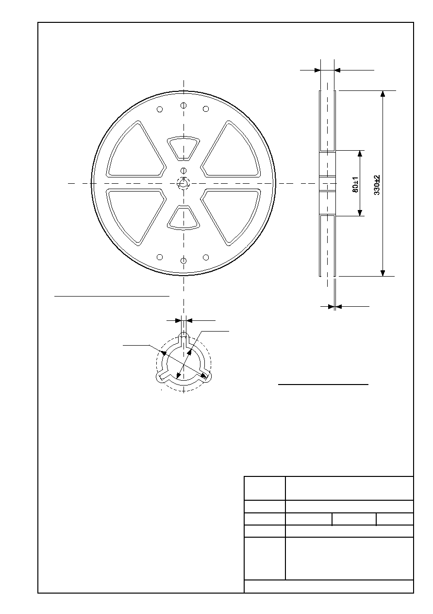
2±0.5
13±0.2
21±0.8
2±0.5
13.5±0.5
QTY.
2,000
No.
TITLE
SCALE
UNIT
mm
Seiko Instruments Inc.
Enlarged drawing in the central part
SSOP10-A-Reel
No. FS010-A-R-SD-1.1
FS010-A-R-SD-1.1

∑
The information described herein is subject to change without notice.
∑
Seiko Instruments Inc. is not responsible for any problems caused by circuits or diagrams described herein
whose related industrial properties, patents, or other rights belong to third parties. The application circuit
examples explain typical applications of the products, and do not guarantee the success of any specific
mass-production design.
∑
When the products described herein are regulated products subject to the Wassenaar Arrangement or other
agreements, they may not be exported without authorization from the appropriate governmental authority.
∑
Use of the information described herein for other purposes and/or reproduction or copying without the
express permission of Seiko Instruments Inc. is strictly prohibited.
∑
The products described herein cannot be used as part of any device or equipment affecting the human
body, such as exercise equipment, medical equipment, security systems, gas equipment, or any apparatus
installed in airplanes and other vehicles, without prior written permission of Seiko Instruments Inc.
∑
Although Seiko Instruments Inc. exerts the greatest possible effort to ensure high quality and reliability, the
failure or malfunction of semiconductor products may occur. The user of these products should therefore
give thorough consideration to safety design, including redundancy, fire-prevention measures, and
malfunction prevention, to prevent any accidents, fires, or community damage that may ensue.