 | –≠–ª–µ–∫—Ç—Ä–æ–Ω–Ω—ã–π –∫–æ–º–ø–æ–Ω–µ–Ω—Ç: S-4543A | –°–∫–∞—á–∞—Ç—å:  PDF PDF  ZIP ZIP |

Contents
Features.............................................................. 1
Block Diagram..................................................... 1
Pin Assignment ................................................... 2
Operating Frequency .......................................... 2
Pad Assignment.................................................. 3
Absolute Maximum Ratings................................. 6
DC Characteristics .............................................. 6
AC Characteristics .............................................. 7
Operation ............................................................ 10
Commands.......................................................... 17
Frequency Characteristics................................... 23
Application Circuit Examples ............................... 24
Examples of Connetction to LCD Panel .............. 25

Seiko Instruments Inc.
1
The S-4543A is a dot matrix liquid crystal display driver IC having an 8-
bit MPU interface, serial interface, display RAM, CR oscillator, 120
segment driver outputs, and 33 common driver outputs. Since it
operates at a low voltage and low current, it is optimum for the LCD
drivers for the portable equipment.
Dot Matrix LCD Driver
S-4543A
Figure 1 Block Diagram
FEATURES
∑
Wide operating voltage range
Logic power supply voltage: -2.4 to -5.5 V
LCD drive voltage: -2.7 to -11.5 V
∑
Built-in CR oscillation circuit: 18 kHz
∑
120 segments, 32 common driver outputs, one common
output for icon
∑
8-bit
◊
120-segment
◊
4-page
+120 segments for Icon
∑
1/32 duty or 1/33 duty selectable
∑
68 family MPU interface
∑
Serial interface
∑
Shipping:
TCP
Bare chip with gold bumps
LCD drive circuit
Common decoder
Display data RAM
4026 bit
Input/o
utput
Line
address
decoder
Column address decoder
Column address counter
Column address register
Common counter
Display line
register
Display timing
generator
Status
Bus
holder
Command
decoder
Row address
decoder
Display data latch
CR OSC
COM
0
to COM
31
SEG
0
to SEG
119
V
1
to V
5
OSC
2
OSC
1
Counter
line
COMICN
P/SX
R/WX
E2
E1
C3/2X
MPU interface
A
0
D
0
to D
7
BLOCK DIAGRAM

Dot Matrix LCD Driver
S-4543A
2
Seiko Instruments Inc.
PIN ASSIGNMENT
OPERATING FREQUENCY
Table 2 Operating Frequency
Operating Frequency
Internal oscillation
External clock
18 kHz
18 kHz
Pin No.
Pin name
Description
36, 37
V
SS
Power supply, negative
53, 54
V
DD
Power supply, positive
57, 59, 61,
64, 65
V
1
to V
5
Power supply pins for driving the liquid crystal. The voltage levels applied must be in
the order shown below:
V
DD
V
1
V
2
V
3
V
4
V
5
25
A
0
Switching signal input between data display and control command display. Normally,
the least significant bit of the address bus of MPU is connected.
A
0
="0"
: D
0
to D
7
are provided for control command input and status output.
A
0
="1"
: D
0
to D
7
are provided for displayed data I/O.
27
OSC
1
CR oscillator input. An oscillator resister R
f
is connected.
An external clock can be input.
29
OSC
2
CR oscillator output. An oscillator resister R
f
is connected.
When an external clock is input, the OSC
2
pin is open.
31
E1
Enable input pin 1.
Enables displayed data RAM corresponding to SEG0 to SEG60 both for the parallel
interface and serial interface.
Active "L".
33
E2
Enable input pin 2.
Enables displayed data RAM corresponding to SEG61 to SEG119 both for the parallel
interface and serial interface.
Active "L".
35
R/WX
Read/write signal input
R/WX="H"
: Read
R/WX="L"
: Write
D
0
to D
7
P/SX : "H" 8-bit data bus connection
tri-state I/O configuration
P/SX : "L" serial interface connection
D0
Serial data input
D1
Clock input
D2
Serial data input
D3 to D7
Open
51
TEST
Test pin. This pin must be connected to V
DD
because "Low" setting of this pin enters to
test mode.
3
C3/2X
Duty selection.
C3/2X="H"
: 1/33 duty. Can be displayed by icon.
C3/2X="L"
: 1/32 duty
58
P/SX
Parallel interface/serial interface switching
P/SX="H" : 8-bit interface
P/SX="L"
: Serial interface
SEG
0
to SEG
119
Segment drive output
COM
0
to COM
31
Common drive output.
Output in the order COM
0
to COM
31
.
66
COMICN
Common drive output for icon.
Output when 1/33 duty is selected.
DUMMY
Insulated from the inside of the IC.
Table 1 Pin Assignment
Dot Matrix LCD Driver
S-4543A
Seiko Instruments Inc.
3
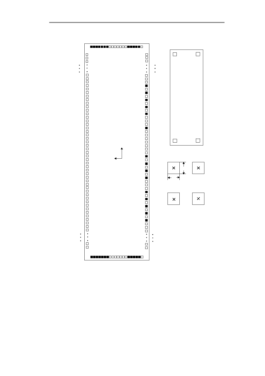
PAD ASSIGNMENT
Figure 2 Pad Configuration
COM outputs:
29
27
25
30
28
26
24
Y
∑
Chip size:
9.3
◊
2.94 mm
∑
Pad pitch:
100
µ
m
∑
Gold bump size:
70
◊
110
µ
m
∑
Gold bump height:
22
±
7
µ
m
∑
Chip thickness:
400
±
30
µ
m
Note: Connect TEST pin to V
DD.
A
C
B
D
Chip Identification Marks
(The identification marks are
larger than the actual scaling.)
(4356, 1356)
X
(0, 0)
23
29
31
33
35
30
32
34
SEG output
(4356,- 1356)
(-4356, 1356)
(-4356,- 1356)
Unit:
µ
m
100
100
108
109
90
89
1
216
198
197
36
COM31
COM22
COM21
COM20
COM0
COMICN
V1
DUMMY
V4
DUMMY
V2
DUMMY
V3
DUMMY
V5
DUMMY
PSX
VDD
VDD
DUMMY
TEST
D7
D6
D5
D4
D3
D2
DUMMY
D1
DUMMY
D0
DUMMY
C32X
DUMMY
RWX
VSS
VSS
DUMMY
ENB2
DUMMY
ENB1
DUMMY
OSC2
DUMMY
OSC1
DUMMY
AO
SEG60
SEG59
SEG38
SEG37
SEG61
SEG62
SEG82
SEG83
SEG84
SEG85
SEG86
SEG87
SEG88
SEG89
SEG90
SEG91
SEG92
SEG93
SEG94
SEG95
SEG96
SEG97
SEG98
SEG99
SEG100
SEG101
SEG102
SEG103
SEG104
SEG105
SEG106
SEG107
SEG108
SEG109
SEG110
SEG111
SEG112
SEG113
SEG114
SEG115
SEG116
SEG117
SEG118
SEG119
SEG0
SEG1
SEG2
SEG3
SEG4
SEG5
SEG6
SEG27
SEG28

Dot Matrix LCD Driver
S-4543A
4
Seiko Instruments Inc.
Table 3 Pin Coordinates
Pin No.
Pin name
X
Y
Pin No.
Pin name
X
Y
1
SEG37
-4400
-1329
55
P/SX
1000
-1329
2
SEG38
-4300
-1329
56
Dummy
1100
-1329
3
SEG39
-4200
-1329
57
V5
1200
-1329
4
SEG40
-4100
-1329
58
Dummy
1300
-1329
5
SEG41
-4000
-1329
59
V3
1400
-1329
6
SEG42
-3900
-1329
60
Dummy
1500
-1329
7
SEG43
-3800
-1329
61
V2
1600
-1329
8
SEG44
-3700
-1329
62
Dummy
1700
-1329
9
SEG45
-3600
-1329
63
V4
1800
-1329
10
SEG46
-3500
-1329
64
Dummy
1900
-1329
11
SEG47
-3400
-1329
65
V1
2000
-1329
12
SEG48
-3300
-1329
66
COMICN
2100
-1329
13
SEG49
-3200
-1329
67
COM0
2200
-1329
14
SEG50
-3100
-1329
68
COM1
2300
-1329
15
SEG51
-3000
-1329
69
COM2
2400
-1329
16
SEG52
-2900
-1329
70
COM3
2500
-1329
17
SEG53
-2800
-1329
71
COM4
2600
-1329
18
SEG54
-2700
-1329
72
COM5
2700
-1329
19
SEG55
-2600
-1329
73
COM6
2800
-1329
20
SEG56
-2500
-1329
74
COM7
2900
-1329
21
SEG57
-2400
-1329
75
COM8
3000
-1329
22
SEG58
-2300
-1329
76
COM9
3100
-1329
23
SEG59
-2200
-1329
77
COM10
3200
-1329
24
SEG60
-2100
-1329
78
COM11
3300
-1329
25
AO
-2000
-1329
79
COM12
3400
-1329
26
Dummy
-1900
-1329
80
COM13
3500
-1329
27
OSC1
-1800
-1329
81
COM14
3600
-1329
28
Dummy
-1700
-1329
82
COM15
3700
-1329
29
OSC2
-1600
-1329
83
COM16
3800
-1329
30
Dummy
-1500
-1329
84
COM17
3900
-1329
31
E1
-1400
-1329
85
COM18
4000
-1329
32
Dummy
-1300
-1329
86
COM19
4100
-1329
33
E2
-1200
-1329
87
COM20
4200
-1329
34
Dummy
-1100
-1329
88
COM21
4300
-1329
35
R/WX
-1000
-1329
89
COM22
4400
-1329
36
VSS
-900
-1329
90
COM23
4509
-900
37
VSS
-800
-1329
91
Dummy
4509
-800
38
Dummy
-700
-1329
92
Dummy
4509
-700
39
C3/2X
-600
-1329
93
Dummy
4509
-600
40
Dummy
-500
-1329
94
Dummy
4509
-500
41
D0
-400
-1329
95
Dummy
4509
-400
42
Dummy
-300
-1329
96
COM24
4509
-300
43
D1
-200
-1329
97
COM25
4509
-200
44
Dummy
-100
-1329
98
COM26
4509
-100
45
D2
0
-1329
99
COM27
4509
0
46
D3
100
-1329
100
COM28
4509
100
47
D4
200
-1329
101
COM29
4509
200
48
D5
300
-1329
102
COM30
4509
300
49
D6
400
-1329
103
Dummy
4509
400
50
D7
500
-1329
104
Dummy
4509
500
51
TEST
600
-1329
105
Dummy
4509
600
52
Dummy
700
-1329
106
Dummy
4509
700
53
VDD
800
-1329
107
Dummy
4509
800
54
VDD
900
-1329
108
Dummy
4509
900

Dot Matrix LCD Driver
S-4543A
Seiko Instruments Inc.
5
Pin No.
Pin name
X
Y
Pin No.
Pin name
X
Y
109
COM31
4400
1329
163
SEG114
-1000
1329
110
SEG61
4300
1329
164
SEG115
-1100
1329
111
SEG62
4200
1329
165
SEG116
-1200
1329
112
SEG63
4100
1329
166
SEG117
-1300
1329
113
SEG64
4000
1329
167
SEG118
-1400
1329
114
SEG65
3900
1329
168
SEG119
-1500
1329
115
SEG66
3800
1329
169
SEG0
-1600
1329
116
SEG67
3700
1329
170
SEG1
-1700
1329
117
SEG68
3600
1329
171
SEG2
-1800
1329
118
SEG69
3500
1329
172
SEG3
-1900
1329
119
SEG70
3400
1329
173
SEG4
-2000
1329
120
SEG71
3300
1329
174
SEG5
-2100
1329
121
SEG72
3200
1329
175
SEG6
-2200
1329
122
SEG73
3100
1329
176
SEG7
-2300
1329
123
SEG74
3000
1329
177
SEG8
-2400
1329
124
SEG75
2900
1329
178
SEG9
-2500
1329
125
SEG76
2800
1329
179
SEG10
-2600
1329
126
SEG77
2700
1329
180
SEG11
-2700
1329
127
SEG78
2600
1329
181
SEG12
-2800
1329
128
SEG79
2500
1329
182
SEG13
-2900
1329
129
SEG80
2400
1329
183
SEG14
-3000
1329
130
SEG81
2300
1329
184
SEG15
-3100
1329
131
SEG82
2200
1329
185
SEG16
-3200
1329
132
SEG83
2100
1329
186
SEG17
-3300
1329
133
SEG84
2000
1329
187
SEG18
-3400
1329
134
SEG85
1900
1329
188
SEG19
-3500
1329
135
SEG86
1800
1329
189
SEG20
-3600
1329
136
SEG87
1700
1329
190
SEG21
-3700
1329
137
SEG88
1600
1329
191
SEG22
-3800
1329
138
SEG89
1500
1329
192
SEG23
-3900
1329
139
SEG90
1400
1329
193
SEG24
-4000
1329
140
SEG91
1300
1329
194
SEG25
-4100
1329
141
SEG92
1200
1329
195
SEG26
-4200
1329
142
SEG93
1100
1329
196
SEG27
-4300
1329
143
SEG94
1000
1329
197
SEG28
-4400
1329
144
SEG95
900
1329
198
Dummy
-4509
900
145
SEG96
800
1329
199
Dummy
-4509
800
146
SEG97
700
1329
200
Dummy
-4509
700
147
SEG98
600
1329
201
Dummy
-4509
600
148
SEG99
500
1329
202
Dummy
-4509
500
149
SEG100
400
1329
203
Dummy
-4509
400
150
SEG101
300
1329
204
SEG29
-4509
300
151
SEG102
200
1329
205
SEG30
-4509
200
152
SEG103
100
1329
206
SEG31
-4509
100
153
SEG104
0
1329
207
SEG32
-4509
0
154
SEG105
-100
1329
208
SEG33
-4509
-100
155
SEG106
-200
1329
209
SEG34
-4509
-200
156
SEG107
-300
1329
210
SEG35
-4509
-300
157
SEG108
-400
1329
211
Dummy
-4509
-400
158
SEG109
-500
1329
212
Dummy
-4509
-500
159
SEG110
-600
1329
213
Dummy
-4509
-600
160
SEG111
-700
1329
214
Dummy
-4509
-700
161
SEG112
-800
1329
215
Dummy
-4509
-800
162
SEG113
-900
1329
216
SEG36
-4509
-900
Table 3 Pin Coordinates (continued)

Dot Matrix LCD Driver
S-4543A
6
Seiko Instruments Inc.
ABSOLUTE MAXIMUM RATINGS
Table 4 Absolute Maximum Ratings
Parameter
Symbol
Ratings
Unit
Supply voltage
V
SS
-
6.0 to +0.4
V
LCD drive voltage 1
V
5
-
13.5 to +0.4
V
LCD drive voltage 2
V
1
, V
2
, V
3
, V
4
V
5
to +0.4
V
Input voltage
V
IN
V
SS
-
0.4 to +0.4
V
Output voltage
V
OUT
V
SS
-
0.4 to +0.4
V
Power dissipation
P
D
250
mW
Operating temperature
T
opr
-
30 to +85
∞
C
Storage temperature
T
stg
-
65 to +150
∞
C
Note 1: When a voltage over the absolute maximum rating is applied, the characteristics of the device may be drastically
aggravated or the chip may be broken.
Note 2: It is recommended to use the device within the range of electrical characteristics. When it is used out of the range, the
operations and the reliability of the device cannot be guaranteed.
DC CHARACTERISTICS
Note 1
V
DD
V
1
V
2
V
3
V
4
V
5
.
Note 2
Drastic fluctuation by power supply voltage, input signal voltage noise, etc. causes malfunction and normal operation
can not be guaranteed. In any case, avoid intentionally changing the power supply voltage during operation.
Note 3
TTL input pins: A
0
, D
0
to D
7
, R/WX, E1, E2.
Note 4
CMOS input pins: C3/2X, P/SX
Note 5
D
0
to D
7
Note 6
Input pins: A
0
, E1, E2, R/WX, OSC
1
, C3/2X
Note 7
Input and output pins at high impedance: D
0
to D
7
.
Note 8
This is the resistance when applying 0.1 V between the LCD drive output pins (SEG
0
to SEG
119
,
COM
0
to
COM
31
,
COMICN) and the LCD drive power pins (V
1
, V
2
,V
3
, and V
4
pins). R
ON
is measured between the LCD drive power pins
and the LCD drive output pins whose electric potential is the same as that of the LCD drive power pins.
Parameter
Symbol
Conditions
Min.
Typ.
Max.
Unit
Note
Operating voltage
V
SS
-
5.5
-
-
2.4
V
Note 1, 2
Recommended
operating voltage
V
SS
-
5.5
-
5.0
-
4.5
V
Note 14
V
5
-
11.5
-
-
2.7
V
Note 1, 2
LCD drive voltage
V
1
, V
2
0.6
◊
V
5
-
V
DD
V
V
3
, V
4
V
5
-
0.4
◊
V
5
V
V
IHT
V
SS
+2.0
-
V
DD
V
Note 3, 13
V
IHC
0.2
◊
V
SS
-
V
DD
V
Note 4, 13
V
ILT
V
SS
-
V
SS
+0.8
V
Note 3, 13
V
ILC
V
SS
-
0.8
◊
V
SS
V
Note 4, 13
V
OH1
I
OH
=-0.5 mA
V
SS
+2.4
-
-
V
Note 5
V
OH2
I
OH
=-120
µ
A
0.2
◊
V
SS
-
-
V
OSC
2
V
OL1
I
OL
=0.5 mA
-
-
V
SS
+0.4
V
Note 5
V
OL2
I
OL
=120
µ
A
-
-
0.8
◊
V
SS
V
OSC
2
Input leakage current
I
IL
-
1.0
-
1.0
µ
A
Note 6
Output leakage current
I
OL
-
3.0
-
3.0
µ
A
Note 7
LCD driver ON
resistance
R
ON
Ta=25
∞
C
V
5
=
-
8.0 V
-
5.0
7.5
k
SEG
0
to SEG
119
COM
0
to COM
31
Note 8
Standby current
I
S
CSX=CL=V
DD
-
0.05
1.0
µ
A
Note 9
I
DD1
During display,
V
5
=
-
5.0V
R
f
=1 M
-
20.0
30.0
µ
A
Note 10
I
DD2
During access, t
CYC
=200
kHz
-
300
500
µ
A
Note 11
R
f
=1.0 M
, V
SS
=
-
5.0 V
15
18
21
kHz
R
f
=1.0 M
, V
SS
=
-
3.0 V
11
16
21
kHz
Wait time
t
w
1000
-
-
µ
s
Note 12
Table 5 DC Characteristics
(Unless otherwise specified : V
DD
=0 V, V
SS
=
-
5.0
±
0.5 V, Ta=
-
20 to 75
∞
C)
High level input
voltage
Low level input voltage
High level output
voltage
Low level output
voltage
Current consumption
Oscillating frequency
f
OSC

Dot Matrix LCD Driver
S-4543A
Seiko Instruments Inc.
7
Note 9
Current consumption when circuits, e.g. the oscillation circuit, the MPU interface, etc, are not operating.
Note 10 Current consumption by LCD panel and parasitic capacitance is not included.
Note 11 Current consumption when writing vertically-striped display data at t
CYC
=200 kHz. After the termination of command,
the current consumption value is I
DD1
.
Note 12 Shows the wait time from when the power voltage rise to 80% of the specfied voltage to when the command input
becomes available.
Note 13 Indicates the inversion level of input signal. The input signal must fully swing in the supply voltage range.
Note 14 When using a power supply voltage other than
-
5.0
±
0.5 V, the value is different. Check the power supply voltage.
AC CHARACTERISTICS
1. Parallel Interface Read/Write
∑
V
SS
=
-
5 V
∑
V
SS
=
-
3 V
Parameter
Sym.
Signal
Conditions
Min.
Max.
Unit
System cycle time
t
CYC6
1000
ns
Address hold time
t
AH6
20
ns
Address setup time
t
AW6
60
ns
Data setup time
t
DS6
100
ns
Data hold time
t
DH6
20
ns
Access time
t
ACC6
CL=15pF
110
ns
Output disable time
t
OH6
CL=15pF
10
130
ns
READ
120
ns
WRITE
120
ns
READ
120
ns
WRITE
120
ns
Parameter
Sym.
Signal
Conditions
Min.
Max.
Unit
System cycle time
t
CYC6
2000
ns
Address hold time
t
AH6
40
ns
Address setup time
t
AW6
120
ns
Data setup time
t
DS6
220
ns
Data hold time
t
DH6
40
ns
Access time
t
ACC6
CL=15pF
220
ns
Output disable time
t
OH6
CL=15pF
10
260
ns
READ
240
ns
WRITE
240
ns
READ
240
ns
WRITE
240
ns
Table 6 AC Characteristics at VSS=
-
5 V
(Ta=
-
20 to 75
∞
C, V
SS
=
-
5 V
±
10%)
A
0
, RWX
(R/W)
E1, E2
D
0
to D
7
Enable pulse width (H)
E1, E2
Table 7 AC Characteristics at VSS=
-
3 V
(Ta=
-
20 to 75
∞
C, V
SS
=
-
3 V
±
10%)
A
0
, RWX
(R/W)
E1, E2
D
0
to D
7
Enable pulse width (H)
t
EWH
Enable pulse width (L)
t
EWL
E1, E2
t
AW6
t
DS6
t
ACC6
t
OH6
A
0
RWX
(R/W)
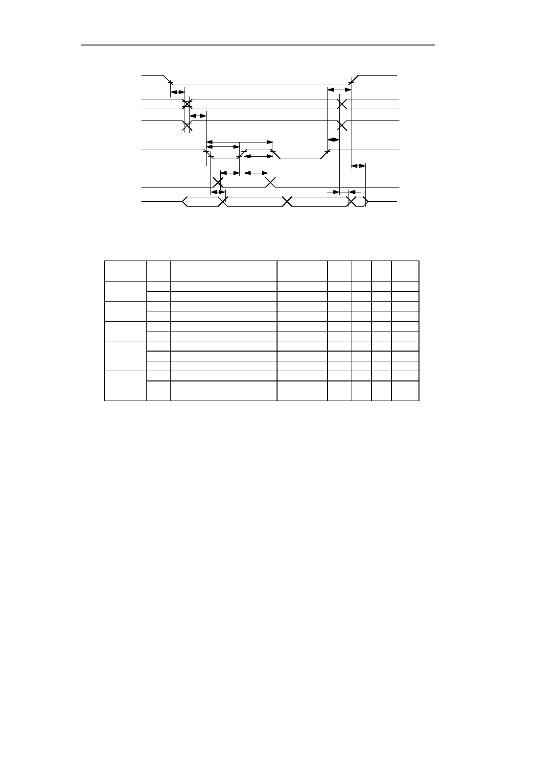
Figure 3 Read/Write Timing with 68-Family MPU
t
EWH
D
0
to D
7
(WRITE)
D
0
to D
7
Enable pulse width (L)
(READ)
t
EWL
t
EW
t
AH6
t
DH6
t
EWL
E1, E2
Dot Matrix LCD Driver
S-4543A
8
Seiko Instruments Inc.
2. Serial Interface
Signal
Symbol
Name
Conditions
Min.
Max.
Unit Remark
s
t
ESS
Enable set-up time
100
ns
t
EHS
Enable hold time
400
ns
t
ASS
Address set-up time
120
ns
t
AHS
Address hold time
200
ns
t
DSS
Data set-up time
120
ns
t
DHS
Data hold time
50
ns
t
CYCS
Clock cycle time
500
ns
t
CLLS
Clock L time
200
ns
t
CLHS
Clock H time
200
ns
t
DDS
Data delay time
CL=15 pF
110
ns
t
OHS1
Data disable time 1
CL=15 pF
0
50
ns
Note 1
t
OHS2
Data disable time 2
CL=15 pF
0
50
ns
Note 2
Figure 4 Serial Interface Read/Write Timing Characteristics
t
ESS
t
ASS
t
CLLS
t
CYCS
t
EHS
t
AHS
t
CLHS
t
DHS
t
DSS
t
DDS
t
OHS1
t
OHS2
E1, E2
D1
(SCLK)
D0
(SDI)
A0
R/WX
D2
(SDO)
Table 8 VSS=-5V Serial Interface Timing Characteristics
(Ta=-30 to 85
∞
C, V
SS
=-5V
±
10%)
E1, E2
D1
(SCLK)
A0, R/WX
D0
(SDI)
D2
(SDO)

Dot Matrix LCD Driver
S-4543A
Seiko Instruments Inc.
9
Note 1: D2(SDO) is uncertain when AO and R/WX change.
Note 2: D2(SDO) enters the high-impedance state at the positive edge of E1 and E2.
Important
* The rise time and decay time of input signal is 15 nsec or less.
* The timing is stipulated by the 20% and 80% of signal waveform.
Signal
Symbol
Name
Conditions
Min.
Max.
Unit Remark
s
t
ESS
Enable set-up time
200
ns
t
EHS
Enable hold time
800
ns
t
ASS
Address set-up time
240
ns
t
AHS
Address hold time
400
ns
t
DSS
Data set-up time
240
ns
t
DHS
Data hold time
100
ns
t
CYCS
Clock cycle time
1000
ns
t
CLLS
Clock L time
400
ns
t
CLHS
Clock H time
400
ns
t
DDS
Data delay time
CL=15 pF
220
ns
t
OHS1
Data disable time 1
CL=15 pF
0
100
ns
Note 1
t
OHS2
Data disable time 2
CL=15 pF
0
100
ns
Note 2
Table 9 VSS=-3V serial interface timing characteristics
(Ta=-30 to 85
∞
C, V
SS
=-3V
±
10%)
E1, E2
D1
(SCLK)
A0, R/WX
D0
(SDI)
D2
(SDO)

Dot Matrix LCD Driver
S-4543A
10
Seiko Instruments Inc.
OPERATION
1. Power-on and off
1.1 Power-on
After power-on, set the default parameters through command input. Input the display off command immediately
after the CPU starts. Set other parameters in order until the display starts. The C3/2X pin must be connected to
V
DD
or V
SS
for use. The recommended procedures after power-on, are as follows:
1. Display ON/OFF
D0: 0
Display OFF
2. Full display ON/OFF
D0: 0
Full display OFF (start of oscilation)
3. End command input
4. ADC selection
5. Display start line
6. Page address "0000"
7. Column address "0000000"
8. Write display data *
9. Display ON
D0: 1
Display ON (start of display)
* After power-on, write display data to all addresses of the display RAM before setting the display to ON because
display RAM is not defined at start up.
1.2 Power-off
Power-off after setting display OFF through a CPU command. The recommended procedures at power-off are
as follows:
1. Display ON/OFF
D0: 0
Display OFF
Note:
After power-on, the parameters except display data RAM are initialized by the operation of the
internal reset circuit. The reset circuit operates at the positive edge of the power-on from ground
voltage level. The operation of the reset circuit can not be guaranteed when the power does not rise
from ground voltage level because of residual voltage from a momentary power failure or continuous
power-on operations.
2. MPU Interface Select
In the S-4543A series, the 8-bit interface or serial interface can be selected.
Table 10 MPU Interface Select
P/SX pin logic
MPU interface
H
68-family interface
L
Serial interface
Note: The displayed data write instruction and displayed data read instruction cannot be executed with E1 and E2
active at the same time.

Dot Matrix LCD Driver
S-4543A
Seiko Instruments Inc.
11
2.1 Parallel Interface
P/S
:
"H" Parallel Interface (Connected to VDD)
E1, E2 :
Operation at the Falling Edge
R/WX
:
"L"WRITE Command, "H"READ Command
A0
:
"L" Command Data, "H" Display Data
D0 to D7:
Date Bus
Note : When reading the command or display data, NEVER input a signal to E1 and E2 simultaneously.
Names of Pins of the S4543A
A0
E1, E2 R / WX
D0 to D7
Names of Signals of 68 Family MPU
A0
E
R / W
D0 to D7
Table 11 Pin Connection for MPU Interface
Figure 5 Read/Write Timings of Parallel Interface Display Data
A0
R/WX
E1, E2
Data bus
MP
Bus holder
Internal
timing
Address Data
Address Set
N Address
Dummy
Read
Display Data
Read
N Address
Display Data
Read
N+2 Address
Display Data Read
Dummy Data
Display Data n
Display Data n+1
Dummy
Data
Display Data n
Display Data n+1
Internal operation
(busy)
A0
R/WX
E1, E2
Data bus
MP
Bus holder
Internal operation
(busy)
Internal
timing
Address N
Display Data n
Display Data n+1
Display Data n+2
Address Set
N addres
s
Display Data
Write
N Address
Display Data
Write
N+1 Address
Display Data
Write
N+2 Address
Display Data Write

Dot Matrix LCD Driver
S-4543A
12
Seiko Instruments Inc.
2.2 Serial Interface
P / SX
: Serial interface (Connected to VSS).
E1, E2
: "L" active.
"H" is reset.
R / WX
: "L" write instruction.
"H" read instruction.
A0
: "L" command data.
"H" displayed data.
D0
: Serial data input pin (SDI)
D1
: Serial clock input pin (SCLK)
D2
: Serial data output pin (SDO)
D3
D7
: Open
Note: The displayed data write instruction and read instruction cannot activate E1 and E2 at the same time.
By setting P/SX to "L", the serial interface is selected.
The instruction code is the same as for the parallel interface.
By setting E1, and E2 to "H", the serial interface circuit is reset and the counter is initialized. Either E1 or E2 is
set to "L", the serial interface enters an operating state.
The commands and displayed data are written at the rising edge of serial clock. Data is input in the order D0 to
D7 in 8-bit data. The status and displayed data are read at the falling edge of the serial clock.
Further, displayed data reading needs dummy reading.
E1 and E2 cannot be set to "L" at the same time when displayed data is written or read out.
Status reading in a reset operation is invalidated at the time the serial interface is selected. However, "H" is
output to the D2 pin (SD0: serial data output pin).
Serial clock wiring must be made by considering external noise and reflecting noise. Be sure to check the
operation of the equipment.
A0
RWX
D0 (SDI)
D2 (SDO)
0
0
Command write
Status read
0
1
Invalid
Status read
1
0
Data write
Status read
1
1
Invalid
Data read (Note)
A0
R / WX
Operation
L
L
Command input
H
H
Displayed data reading
L
H
Status reading
H
L
Displayed data writing
Figure 6 Read/Write Timings of Serial Interface Display Data
D0
D1
D2
D3
D4
D5
D6
D7
A0
R/WX
D1
(SCLK)
D0
(SDI)
E1, E2
D0
D1
D2
D3
D4
D5
D6
D7
D2
(SDO)
Note: Data reading needs dummy reading.
D0
D0

Dot Matrix LCD Driver
S-4543A
Seiko Instruments Inc.
13
3. Status
The internal operation status of S-4543A is monitored for four kinds of status. The status is output in D
4
through
D
7
. For the monitoring method and function, refer to the Command functions section.
E1 and E2 cannot be activated at the same time during status reading.
Table 12 Internal Operation Status
Item
Output pin
Status
Busy flag
D
7
"1": Command operation, Reset operation "0": Command ready
ADC select
D
6
"1":
Forward
"0": Reverse
Display
ON/OFF
D
5
"1": Display all-lit
"0": Normal display status
Reset
D
4
"1": Resetting
"0": Normal operation status
4. Busy Flag
During internal operation, for example command operation, the busy flag is "1", and commands other than Status
Read are not received. The Busy flag is output in D7 through the Status Read command. When accessing the
S-4543A by the signal which specifies the value of read cycle and write cycle timing, the busy flag "0" is not
required to be confirmed. Since busy flag check is not necessary, the load on MPU can be reduced.
5. Data Bus
Table 13 Data Bus
A
0
68 family
R/WX
Operation
1
1
Read from Display Data RAM
1
0
Write to Display Data RAM
0
1
Status Read
0
0
Command Read to internal register
6. Display Data RAM
The S-4543A has Display Data RAM (8 bits X 4 pages X 122 columns + 120 columns for icon =4026 bits). It is
possible to use the not-used area for display as normal SRAM. The Display Data RAM is in dual port RAM and
enables access from the MPU through Page address and Column address. To the LCD driver side, the one line's
common output is read by Line address. The correlation between Page address, Column address, and Line
address is shown in Figure 7.
The displayed data RAM is made of dual-port RAM. The read/write access from the MPU interface is performed
independently of the read access to the liquid display. The read/write access to displayed data from the MPU is
done by a command. Data is read out to the liquid crystal display in synchronism with the liquid crystal display
clock.
At the moment power is turned on, the contents of the displayed data RAM are uncertain. Following turning on
power, clear the display RAM or write the displayed data with display OFF and then turn ON the display.
The displayed data RAM is divided into two parts by E1 and E2. The displayed data can be written into the
column address corresponding to SEG0-SEG60 by E1. E2 enables data writing into the column address
corresponding to SEG61-SEG119.

Dot Matrix LCD Driver
S-4543A
14
Seiko Instruments Inc.
7. Reading and Writing of Display Data
The S-4543A reads and writes the display data through the internal bus holder. The display data is read to the
bus holder from the display data RAM, and in the next read cycle on the data bus. Therefore, a dummy read
cycle is needed before the first read cycle. When reading the display data after the address set and the data write
cycle, a dummy read is needed. Since the reading of the display data is executed using this bus holder, it is
possible to read the data at high speed.
Display data is written to the display data RAM through the bus holder within a write cycle. Therefore, writing the
display data does not need a dummy cycle.
The displayed data is lit and unlit in the states "1" and "0", respectively.
8. Column Address
The column address of the Display Data RAM is used for reading/writing displayed data from/to the MPU. The
column address is set by a command. When the displayed data RAM is accessed by the MPU, the address
increments by one. When the most significant address of the column address is read/written, an invalid address
is selected and it does not increment.
9. Page Address
The display RAM is composed of five pages. When accessing the display data RAM from MPU, the page of the
display data RAM is set a command.
10. CR Oscillation Circuit
It incorporates a CR oscillator which generates the clock for display.
Oscillation frequency is approximately 18 kHz at R
f
1 M
.
11. LCD Driving Circuit
The S-4543A generates a liquid crystal drive waveform of 2-frame AC drive system (type B). See Figure 8, "
Liquid Crystal Drive Output Waveform."
12. Display Timing Circuit
It generates the clock by the CR oscillator circuit or an external input for the timings of the liquid crystal drive. See
Figure 8.
The frame frequency differs depending upon the selection of 1/32 or 1/33 duty ratio.
Table 15 Frame Frequency
Duty
Frame Frequency f
OSC
=18 kHz
1/32 duty
70.31 Hz
1/33 duty
68.18 Hz
13
.
Line Address
This is the address for reading the LCD RAM data to the LCD data latch. The line address is incremented
synchronizing with the common output. Further, the display start line which is output to COM0 can be set by a
command.
14. Display Data Latch
The display data latch is the circuit for latching one line's display data from the display RAM. The display data is
output from this latch to the LCD drive circuit. Since the display ON/OFF and the display All-Lit ON/OFF control
the display data latch, it has no effect on the display RAM data.

Dot Matrix LCD Driver
S-4543A
Seiko Instruments Inc.
15
Figure 7 Relationship between Display Data RAM and Addresses
D
0
D
1
D
2
D
3
D
4
D
5
D
6
D
7
0, 0, 0
Page
address
D
3
,D
2
,D
1
page 0
Line
address
00
H
01
02
03
04
05
06
07
D
0
D
1
D
2
D
3
D
4
D
5
D
6
D
7
0, 0,1
D
0
D
1
D
2
D
3
D
4
D
5
D
6
D
7
0, 1, 0
D
0
D
1
D
2
D
3
D
4
D
5
D
6
D
7
0, 1, 1
08
09
0A
0B
0C
0D
0E
0F
10
11
12
13
14
15
16
17
18
19
1A
1B
1C
1D
1E
1F
page 1
page 2
page 3
SEG terminal
A common output example when
executing the display starting from
08
H
at 1/33 duty:
Display
start
Note:
For the display data RAM of the S-4543A Series, the memory area corresponding to SEG 0 through
SEG119 is valid as display data. The other memory area can be used as normal SRAM.
1, 0, 0
D
0
COMICN
page 4
COM
0
COM
1
COM
2
COM
3
COM
4
COM
5
COM
6
COM
7
COM
8
COM
9
COM
10
COM
11
COM
12
COM
13
COM
14
COM
15
COM
16
COM
17
COM
18
COM
19
COM
20
COM
21
COM
22
COM
23
COMICN
COM
24
COM
25
COM
26
COM
27
COM
28
COM
29
COM
30
COM
31
13
00 01 02 03 04 05 06 07
3C 00
4F 4E4D 4C4B4A 49 48
4F
15
0 1 2 3 4 5 6 7
60 61
119
3A
3B
14
E1 = Active
E2 = Disable
E1 = Active
E2 = Disable
Column
address
13
3
C
ADC
D0=
"0"
ADC
D0=
"1"

Dot Matrix LCD Driver
S-4543A
16
Seiko Instruments Inc.
Display duty
Frame period
duty 1/32
256 / f
OSC
duty 1/33
264 / f
OSC
Figure 8 LCD Driver Waveform Example
0
0
1
1
2
2
3
3
32
COM
ICN
0
0
1
1
2
2
3
3
t
FR
COM
0
COM
1
SEG
0
SEG
1
COM
0
-
V
1
∑|V
-
V
3
-
V
4
-
V
5
COM
0
-
SEG
0
-
SEG
1
V
DD
V
1
V
2
V
3
V
4
V
5
V
DD
V
1
V
2
V
3
V
4
V
5
V
DD
V
1
V
2
V
3
V
4
V
5
V
DD
V
1
V
2
V
3
V
4
V
5
V
5
V
4
V
3
V
2
V
1
V
DD
-
V
1
-
V
2
-
V
3
-
V
4
-
V
5
V
5
V
4
V
3
V
2
V
1
V
DD
31
32
31
32
32
Frame period
COM
ICN
1/32 duty
COM output pin
1/32 duty
COM output pin
Table 14 Frame Period
f
OSC
=CR oscillation frequency

Dot Matrix LCD Driver
S-4543A
Seiko Instruments Inc.
17
COMMANDS
For S-4543A, the command functions can be set by the combination of A
0
and E1, and E2 and R/WX. The
commands are set for S-4543A, by the internal timings different from the instructions of MPU. When displayed data
writing in operational description, read-out timing chart, and timing characteristics chart are satisfied, the commands
can be input without checking the busy flag. Therefore, high speed operation and MPU load reduction are attainable.
For the command list, refer to Table 18.
1. Display ON/OFF
The logic D
0
controls the display ON/OFF. In display OFF, the screen is compelled to be all-off regardless of the
display RAM data. The display RAM data does not change.
In display ON, normal display is on according to the display RAM data. When the display ON command is input,
display OFF is canceled.
When setting display all-lit ON in the display OFF status, it changes to Power save mode (see the Power Save
command.)
2. Display Start Line Set
The line address of the display data RAM which indicates the display start line is set. The display start line
corresponding to COM
0
, as shown in the figure, indicates the correlation between the display data RAM and the
address. The display area read from the display data RAM corresponds to the number of the lines for the duty set
using the Duty select command. The line address is automatically incremented synchronizing with the common
output. Changing the display START line using this command enables a smooth scroll on the screen or a page
change .
3. Page Address Set
The page address is set when accessing the display data RAM from the MPU. It is possible to access the display
data RAM from the MPU using the page address and the column address. Refer to the figure 7 which shows the
correlation between the display data RAM and the address. Even if the page address is changed, it has no
influence, such as changing of the screen during operation.
4. Column Address Set
The column address is set when accessing the display data RAM from the MPU. When accessing the display data
RAM from the MPU, the column address is incremented by one. When accessing the successive column address
from the MPU, it is possible to access the display data without setting the column address each time. The
automatic increment stops after the uppermost column address is accessed.
When selecting "Reverse" using the "ADC select" command, the lowermost column address is 13H; the uppermost
column address is 4FH.

Dot Matrix LCD Driver
S-4543A
18
Seiko Instruments Inc.
5. Status Read
It is possible to read four kinds of status using this command.
6. Write Data
The 8-bit display data is written in the display data RAM. After writing the display data, the column address is
automatically incremented. When writing the successive display data after setting the first column address
using the column address set command, it is unnecessary to set the column address each time.
For the serial interface, the displayed data is written in the unit of 8 bits.
7. Read Data
The 8-bit display data is read from the display data RAM. After reading the display data, the column address is
automatically incremented. When reading the successive display data after setting the first column address
using the column address set command, it is unnecessary to set the column address each time. For reading
display data just after the column address set, a dummy read is needed.
The serial interface also needs dummy reading.
8. ADC Select
Forward or reverse can be selected for the correlation between the column address and the segment output
terminal of the display data RAM. Make sure the RAM corresponds to the address.
D0 D0 : "0"
Forward: The column addresses 0
H
to 3C
H
, which are written when E1 is"H," correspond to the
segment
output terminals starting from 0 to 60;
the column addresses
0
H
to 3A
H
,
which are written
when
E2 is "H
,"correspond to the segment output terminals starting from 61 to 119
.
D0
: "1"
Reverse: The column addresses 13
H
to
4F
H
, which are written when
E1 is "H," correspond to the
segment output terminals starting from 60 to 0;
the column addresses
15
H
to 4F
H
,
which are written
when
E2 is "H
,
"
correspond to the segment output terminals starting from 119 to 61.
Shows the command ready during the S-4543A command operation.
"1" : Shows that the IC inside is executing a command operation or a reset operation.
When the Busy flag is output, the command is not received. If the cycle time of the command is
satisfied with the specified value, Busy flag confirmation is not needed.
"0" : Shows that the command is ready
Shows forward or reverse correlation between column address and segment output terminal of the
display data RAM
The setting is executed using the ADC select command.
"1"
: Forward
The correspondence between the column addresses and segment output pins are
such that:
[1] The column addresses 0
H
to 3C
H
into which data is written at the time E1=active
correspond to the segment outputs 0 to 60.
[2] The column addresses 0
H
to 3A
H
into which data is written at the time E2=active
correspond to the segment outputs 61 to 119.
"0"
: Reverse
The correspondence between the column addresses and segment output pins are
such that:
[1] The column addresses 13
H
to 4F
H
into which data is written at the time E1=active
correspond to the segment outputs 60 to 0.
[2] The column addresses 15
H
-4F
H
into which data is written at the time E2=active
correspond to the segment outputs 119 to 61.
Shows the display ON/OFF status.
Note: it is the reverse to the polarity of Display ON/OFF command.
"0" : Shows the display ON status.
Display normal operation status
"1" : Shows the display OFF status.
Display all-OFF status.
Shows that the S-4543A is executing initialization by RESX input or Reset command.
"0" : Normal operation
"1" : Reset operation
Table 15 Status Read
Busy
ADC
ON/OFF
Reset

Dot Matrix LCD Driver
S-4543A
Seiko Instruments Inc.
19
9. Display All-Lit ON/OFF
Display all-lit ON makes the display be entirely lit. All common outputs become selectable status. Segment output
is compelled to be all-lit output. The display RAM's data, however does not change.
Through Display all-lit OFF, the screen returns to normal display operation.
When inputting the Display OFF command in the display all-lit ON status, it changes to Power save mode (Refer
to the Power save command).
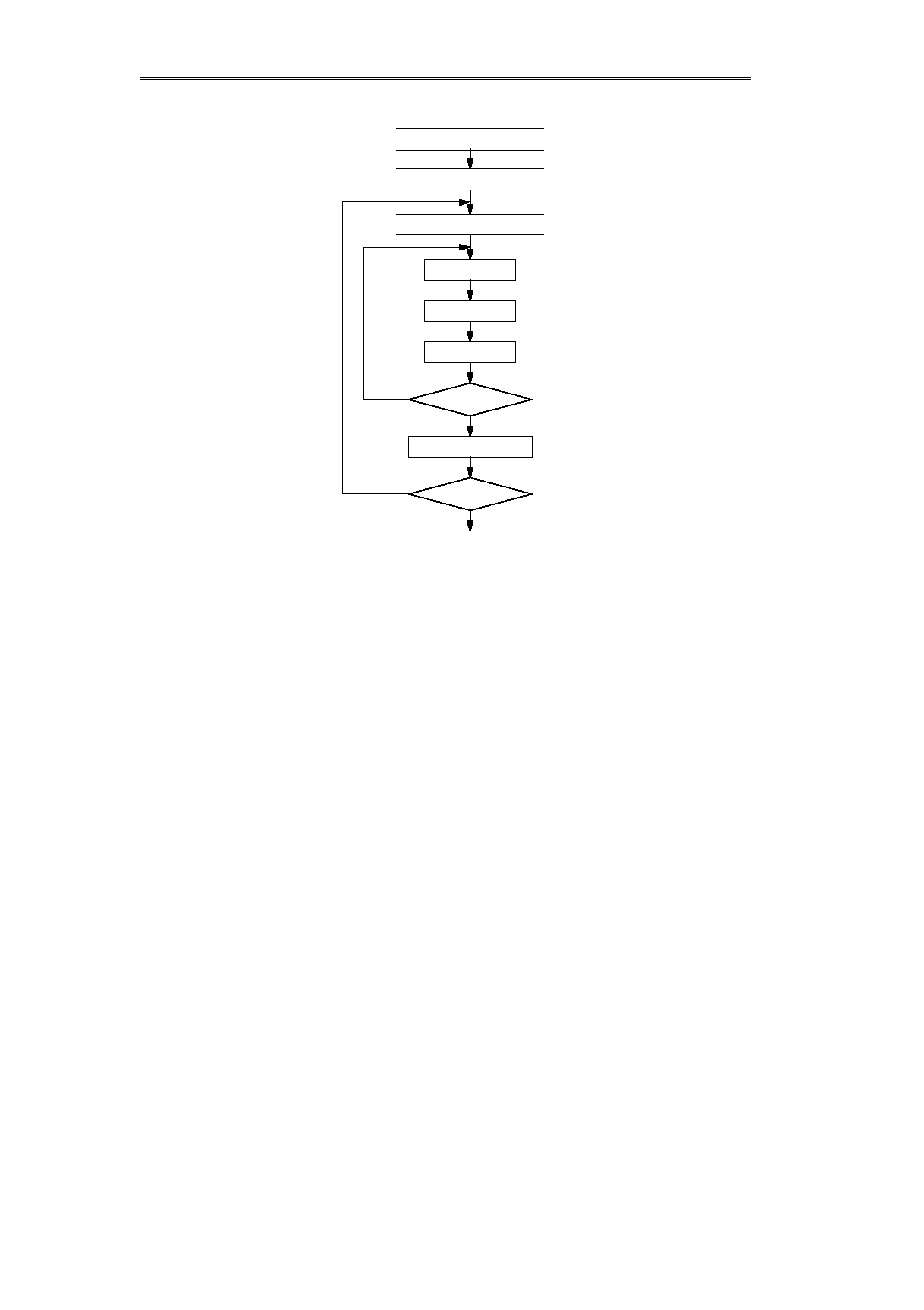
10. Read Modify Write
The read modify write command is valid when partly altering or rewriting the display data RAM, for example the
cursor indication, the blinking indication, etc. After inputting the Read modify write command, column address of
the display data RAM is incremented only when inputting the display data write command. In Read data
command, it is possible to rewrite the display data of the column address which is read, without increment of the
column address. Furthermore, when reading and writing of the display data is successively executed, the
successive address of the display data RAM is rewritten within the same page. A dummy read is needed when
reading the display data.
Read modify write command is valid until the End command is input. When inputting the End command, the
column address returns to the address before the Read modify command was input.
During the Read modify write command operation, all commands are usable except the Column address set
command.
11. End Command
This command cancels Read modify write. The column address of the display data returns to the address prior to
execution of the Read Modify Write command.
Dot Matrix LCD Driver
S-4543A
20
Seiko Instruments Inc.
12. Reset Command
This command resets the address of the display data RAM as follows:
After resetting, display starts according to the reset value.
∑
Resets the Display START Line to the 1st line.
∑
Resets the page address to 3.
Figure 9 Command Sequence for Cursor Indication
Page Address Set
Column Address Set
Read Modify Write
Dummy Read
Data Read
Data Write
Rewrite End
End Command
Rewrite again
NO
End
NO
YES
YES
Returns to the previous address prior to
the execution of Read Modify Write
command using the End command.

Dot Matrix LCD Driver
S-4543A
Seiko Instruments Inc.
21
13. Power Save Mode
When setting display all-OFF using the Display OFF command and executing the Display all-lit ON command, it
changes to the Power save mode. When displaying in all-lit status and executing the Display OFF command, it
also changes to the Power save mode. In the Power save mode,
∑
Current consumption is reduced and a value near that at standstill is attainable.
∑
The LCD drive circuit is stopped. The Segment and Common outputs are fixed at V
DD
level.
∑
nput is prohibited and the OSC
2
terminal floats.
∑
Content of the display data RAM, the command and the address before the power save mode do not
change.
The Power save status is canceled through the Display ON or the Display all-lit commands.
When the LCD driver voltage is generated by division of external resistance, the electric current is passed
through this divided resistance regardless of the ICs. When reducing this current, attach a switching transistor
which cuts the current flowing to the external resistance
.
Table 16 Power Save Commands
Command Combination
Status
Display
Display All-
Lit
ON
OFF
Normal display
operation
ON
ON
All-lit display
OFF
OFF
All-off
OFF
ON
Power save
Notes on command input:
The displayed data RAM reading/writing and status reading are done by activating E1 and E2 independently of
each other.
The commands for inputting data into the liquid crystal display are enabled by activating either E1 or E2.
Table 17 Command Input
Instructions which can
be executed and in
which commands can be
input with E1 and E2
active at the same time
Commands
corresponding to SEG0-
SEG60 and SEG61-119
with E1 or E2 active
Instructions which can
be executed and in
which commands can be
input with either E1 or
E2 is made active
Display ON/OFF
Display Start Line Set
Page Address Set
Column Address Set
Status Read
Prohibited
Display Data Write
Prohibited
Display Data Read
Prohibited
ADC select
Display All Lit/Unlit
Read Modify Write
End
Reset
Power Save

Dot Matrix LCD Driver
S-4543A
22
Seiko Instruments Inc.
Code
Command
A
0
R/W
X
WRX
D
7
D
6
D
5
D
4
D
3
D
2
D
1
D
0
Description
Display ON/OFF 0
0
1
0
1
0
1
1
1
0
/
1
Selects normal display or all off on the screen.
D
0
: 1ON. Normal display operation using
the display data RAM.
D
0
: 0OFF. Display OFF status regardless of
the display RAM data. Power Save
mode is entered by display OFF and
display all-lit ON.
Display START
Line
0
0
1
1
0
Display start line address
(See Table 21)
Sets the line address of the display data RAM
to be displayed at the top line of the screen
(COM
0
output). Address setting ranges from 0
to 31.
Page Address
Set
0
0
1
0
1
1
1
Page address
(See Table 20)
Sets up the page address of the display data
RAM in order to access the display data RAM
from the MPU. Address setting ranges from 0
to 4.
Column
Address Set
0
0
0
Column address
(See Table 21)
Sets up the column address of the display
data RAM in order to access the display data
RAM from the MPU. Address setting ranges
from 0 to 79.
Status Read
0
1
Busy
ADC
Dis-
play
ON/
OFF
Reset
0
0
0
0
Reads the status.
BUSY
1: Command operation
0: Command ready
ADC
1: Column address forward
0: Column address invert
Display
1: Display all-off status
ON/OFF 0: Normal display status
RESET
1: Resetting
0: Normal operation
Write Display
Data
1
0
Data written into the displayed data RAM
Writes the data D
0
through D
7
on the
display data RAM.
Read Display
Data
1
1
Data read from the displayed data RAM
Reads the data D
0
through D
7
from the
display data RAM.
ADC Select
0
0
1
0
1
0
0
0
0
0
/
1
Used to invert the column address of the
display data RAM, after which the correlation
between the display RAM's addresses and
segment output terminals is inverted.
D
0
: 0 Forward
D
0
: 1 Reverse
Display all-lit
ON/OFF
0
0
1
0
1
0
0
1
0
0
/
1
Selects normal display operation or all-lit
display operation.
D
0
: 0 Normal display operation
D
0
: 1 All-lit display operation
The screen is changed to all-lit status. Power
Save mode is entered through display OFF
and display all-lit ON.
Read Modify
Write
0
0
1
1
1
0
0
0
0
0
Increments the column address of display data
RAM only when display data is written but not
when it is read.
End
0
0
1
1
1
0
1
1
1
0
Cancels Read Modify Write mode and
increments the column address of the display
data RAM when display data is written and
read.
Reset
0
0
1
1
1
0
0
0
1
0
Resets the address of the display data RAM
as follows:
∑
Resets the Display START Line to the 1st
line.
∑
Resets the page address to 3.
Table 20 Display Commands
Sets the display RAM's
address using Page Address
Set and Column Address Set.
When accessing the display
data RAM, the column
address is automatically
incremented.

Dot Matrix LCD Driver
S-4543A
Seiko Instruments Inc.
23
Table 21 Display Start Line Address
D
4
D
3
D
2
D
1
D
0
A
4
A
3
A
2
A
1
A
0
0
0
0
0
0
0
0
0
0
0
1
1
.
.
.
.
.
.
.
.
.
.
.
.
.
.
.
.
.
.
1
1
1
1
1
31
Table 22 Page 2Address
D
2
D
1
D
0
A
2
A
1
A
0
0
0
0
0
0
0
1
1
0
1
0
2
0
1
1
3
1
0
0
4
Table 23 Column Address
D
6
D
5
D
4
D
3
D
2
D
1
D
0
A
6
A
5
A
4
A
3
A
2
A
1
A
0
0
0
0
0
0
0
0
0 (0)
H
0
0
0
0
0
0
1
1 (1)
H
.
.
.
.
.
.
.
.
.
.
.
.
.
.
.
.
.
.
.
.
.
.
.
.
1
0
0
1
1
1
1
79 (4F)
H
FREQUENCY CHARACTERISTICS
1. Oscillation Frequency
2. Frame Frequency
Figure 10 Frequency Characteristics
40
30
20
10
0
0.5
1.0
1.5
2.0
2.5
f
OSC
(kHz)
R
f
(M
)
Ta=25
∞
C
200
150
100
50
0
0.5
1.0
1.5
2.0
2.5
Frame
frequency
(Hz)
R
f
(M
)
Ta=25
∞
C
V
SS
=
-
3 V
V
SS
=
-
5 V
V
SS
=
-
3 V
V
SS
=
-
5 V
Line Address
Page Address
Column Address

Dot Matrix LCD Driver
S-4543A
24
Seiko Instruments Inc.
APPLICATION CIRCUIT EXAMPLES
1. 68 Family MPU Interface
2. Serial Interface
Figure 11 68 Family MPU Interface
A
0
A
1
A
15
VMA
E
GND
V
CC
Decoder
A
0
D
0
D
7
D
0
D
7
E1
V
SS
V
DD
S-4543A
Note:
S-4543A has no CSX terminal. The logic for E is
provided externally and does not need to be input.
CSX
P/SX
R/WX
R/WX
E2
V
SS
68
family
MPU
TEST
Figure 12
Serial Interface
A
0
A
1
A
7
GND
V
CC
Decoder
A
0
E1
V
S
V
DD
S-4543A
R/WX
R/WX
E2
SCL
S1
Port 1
Port 2
V
S
P/SX
V
DD
Note:
S-4543A has no CSX terminal. Logic for E must
be set outside.
TEST

Dot Matrix LCD Driver
S-4543A
Seiko Instruments Inc.
25
EXAMPLES OF CONNECTION TO LCD PANEL
Figure 13 EXamples of Connection to LCD Panel
1. 1/32 duty x 24 character x 4 line LCD panel
LCD (32
◊
120)
SEG
S-4543A
1
:
32
COM 0
31
1
120
2. 1/33 duty x 24 character x 4 line+icon LCD panel
LCD (33
◊
120)
SEG
S-4543A
1
:
32
COM 0
31
1
120
ICON
COMIC

Dot Matrix LCD Driver
S-4543A
26
Seiko Instruments Inc.
(This page intentionally blank)