Seiko Instruments Inc.
1
,
The S-4602A is a CMOS thermal print head driver containing a 64-bit
shift register and a latch. The 75
µ
m driver output pad pitch allows for
high density mounting up to 300dpi. It can be used for general purpose
because "H" or "L" can be selected for the latch and the driver enable .
Block Diagram
64-bit THERMAL HEAD DRIVER
S-4602A
∑
Driver output current : 15 mA typ.
(V
OL
=0.7 V, Ta=-10 to 80
∞
C)
∑
64-bit shift register and latch are built in
∑
Driver enable
∑
Driver-off function when supply voltage falls
∑
Selectable
"
H/L
"
for latch and driver enable
Features
∑
Low current consumption : 0.3 mA typ.
(f
CLK
=2 MHz, SI : fixed)
∑
High speed operation : 10 MHz (cascade
connection)
∑
Driver output voltage : 36 V max.
Figure 1
AEN
BEN
V
DD
LATCH
CONT
V
SS0
LA
LA
LA
D-FF
D-FF
LA
LA
SI
CLK
SO
V
SS0
V
DD
DO
1
DO
2
DO
3
DO
63
DO
64
V
SS1
D-FF
D-FF
D-FF
V
SS0
64-bit THERMAL HEAD DRIVER
S-4602A
2
Seiko Instruments Inc.
Operation
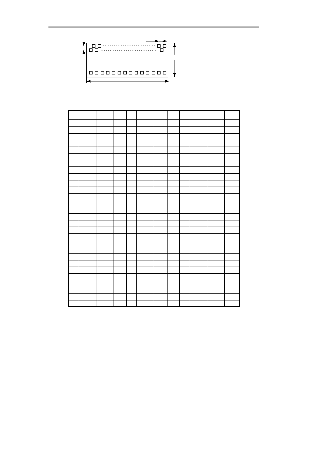
Terminal Functions (Refer to the dimensions for the pad arrangement)
Absolute Maximum Ratings
No.
Name
Functions
1 to 64
DO
1
to DO
64
( DOn)
Driver output terminals (Nch open-drain)
65, 66, 73,
74, 80, 81
V
SS1
GND for driver (0 V)
71, 78
V
DD
Positive power supply for logic (+5 V)
67, 75
V
SS0
GND for logic (0 V)
77
CLK
Clock input terminal for 64-bit shift register
79
SI
Serial data input terminal for 64-bit shift register
68
SO
Serial data output terminal for 64-bit shift register
69
LATCH
Data latch signal input terminal
When CONT=
"
L
"
or open
LATCH=
"
L
"
: reads the data of the shift register
LATCH=
"
H
"
: holds the preceding data
When CONT=
"
H
"
LATCH=
"
L
"
: holds the preceding data
LATCH=
"
H
"
: reads the data of the shift register
72
CONT
Data latch signal control terminal : selects
"
H
"
or
"
L
"
for
LATCH(pull-down resistor is built in)
76
AEN
Driver enable terminal : outputs the latch data to the
driver when
"
L
"
(pull-up resistor is built in)
70
BEN
Driver enable terminal : outputs the latch data to the
driver when
"
H
"
(pull-down resistor is built in)
Parameter
Symbol
Ratings
Unit
Supply voltage
V
SS0,1
- V
DD
-0.4 to +7.0
V
Driver output voltage
V
DOH
36
V
Driver output current
I
DOL
30
mA
Input voltage
V
IN
V
SS0
-0.5 to V
DD
+0.5
V
Output voltage
V
OUT
V
SS0
-0.5 to V
DD
+0.5
V
Max. junction temperature
T
jMAX
125
∞
C
Operating temperature
T
opr
-10 to +80
∞
C
Storage temperature
T
stg
-40 to +125
∞
C
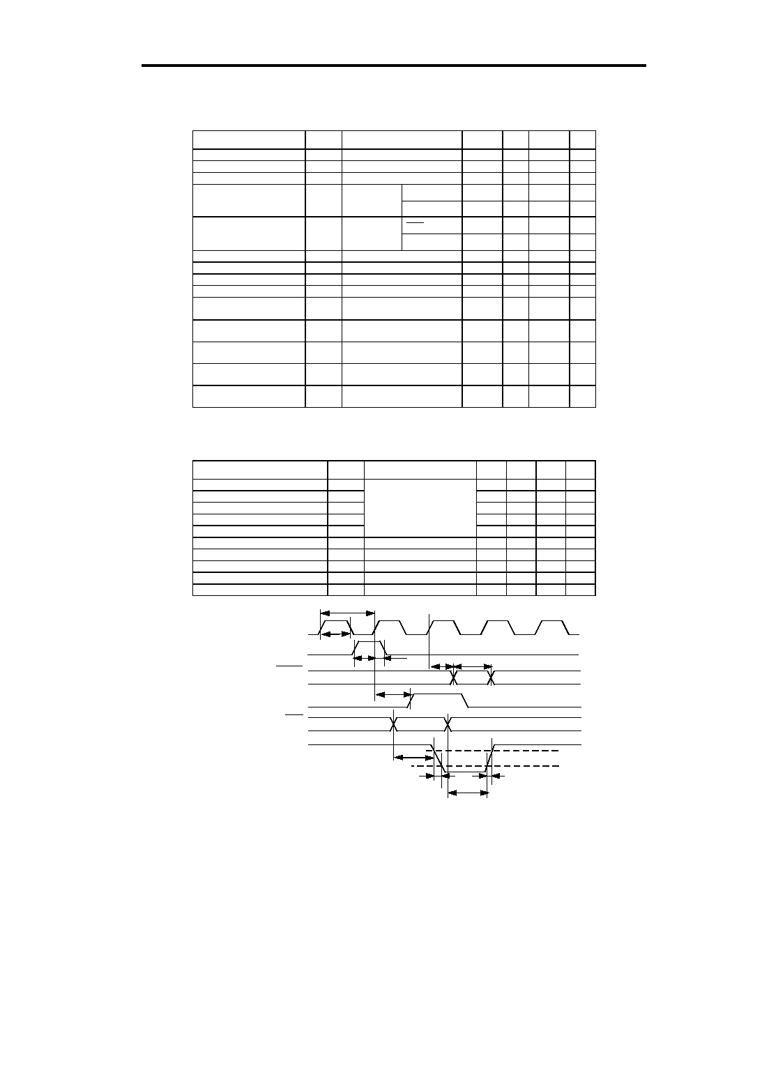
The 64-bit shift register reads the data input to SI on the rising edge of the CLOCK input.
The latch circuit operates depending on the levels of CONT and LATCH ; it reads the data of the shift register
when their levels are the same, and it holds the data of the shift register when they differ.
The latch data are output to the respective drivers when AEN is low and BEN is high. The driver output
transistor turns on when the latch data are high and turns off when low. Turning AEN high or BEN low makes
all driver output transistors go off.
All driver output transistors go off when power supply voltage becomes lower than V
DET
regardless of all input
signals.
Table 1
Table 2
64-bit THERMAL HEAD DRIVER
S-4602A
Seiko Instruments Inc.
3
DC Electrical Characteristics
AC Electrical Characteristics
Table 4
(V
DD
= 5.0 V
±
10%, Ta=-10
∞
C to 80
∞
C)
Parameter
Symbol
Conditions
Min.
Typ.
Max.
Unit
CLK pulse width
t
WCLK
40
ns
Data setup time
t
SUD
V
IH
=V
DD
, V
IL
=V
SS0
40
ns
Data hold time
t
HD
V
IH
=V
DD
, V
IL
=V
SS0
40
ns
Latch pulse width
t
WLA
50
ns
Latch setup time
t
SULA
50
ns
CLK-SO propagation delay time
t
dSO
C
L
=3 pF
60
ns
EN-DOn propagation delay time
t
dDO
R
L
=3 k
, V
DOH
=24 V
4.0
µ
s
DOn rise time
t
rDO
R
L
=3 k
, V
DOH
=24 V
0.7
2.0
µ
s
DOn fall time
t
fDO
R
L
=3 k
, V
DOH
=24 V
0.8
2.2
µ
s
Clock frequency
f
CLK
When cascade connection
10
MHz
Parameter
Symbol
Conditions
Min.
Typ.
Max.
Unit
Supply voltage
V
DD
4.5
5.0
5.5
V
High level input voltage
V
IH
0.8
◊
V
DD
V
DD
V
Low level input voltage
V
IL
V
SS
0.2
◊
V
DD
V
BEN, CONT
17
55
µ
A
0.5
µ
A
AEN
-55
-17
µ
A
-0.5
µ
A
High level output voltage
V
OH
SO terminal, no load
4.45
V
Low level output voltage
V
OL
SO terminal, no load
0.05
V
High level output current
I
OH
SO terminal, V
OH
=V
DD
-0.4 V
-
0.5
mA
Low level output current
I
OL
SO terminal, V
OL
=0.4 V
0.5
mA
High level driver output
voltage
V
DOH
Heat generator
resistance : 1000
24
28
V
Low level driver output
voltage
V
DOL
I
DOL
=15 mA
0.7
1.5
V
Driver leakage current
I
LEAK
V
DOH
=26 V
Per 1-bit of driver output
1.0
µ
A
Current consumption
I
DD
f
CLK
=2 MHz, Ta=25
∞
C
SI : fixed
0.3
1.0
mA
Lower V
DD
detection
voltage
V
DET
0.8
4.0
V
Table 3
(Unless otherwise specified : V
DD
=5.0 V
±
10%, Ta=-10
∞
C to 80
∞
C)
V
DD
=5.0 V
V
IH
=5.0 V
Ta=25
∞
C
V
DD
=5.0 V
V
IL
=0 V
Ta=25
∞
C
Figure 2
I
IH
High level input current
I
IL
Low level input current
CLK
SI
LATCH
SO
LATCH
AEN
BEN
DO
n
1/f
CLK
t
WCLK
t
SUD
t
HD
t
SULA
t
WLA
t
dSO
t
dDO
t
fDO
t
dDO
t
rDO
10%
90%