 | –≠–Ľ–Ķ–ļ—ā—Ä–ĺ–Ĺ–Ĺ—č–Ļ –ļ–ĺ–ľ–Ņ–ĺ–Ĺ–Ķ–Ĺ—ā: S-57 | –°–ļ–į—á–į—ā—Ć:  PDF PDF  ZIP ZIP |
Document Outline
- S-8355/56/57/58 Series
- Cover
- Features
- Packages
- Applications
- Block Diagram
- Selection Guide
- Pin Assignment
- Absolute Maximum Ratings
- Electrical Characteristics
- Test Circuits
- Operation
- External Parts Selection
- Standard Circuits
- Power Dissipation of Package
- Precautions
- Application Circuits
- Example of Major Temperature Characteristics (Ta =-40 to 85įC)
- Example of Major Power Supply Dependence Characteristics (Ta =25įC)
- Output Waveforms
- Examples of Transient Response characteristics
- Reference Data
- Package drawing
- SOT-89-3
- SOT-23-3
- SOT-23-5
- 6-Pin SNB(B)

Rev.4.1
_00
SUPER-SMALL PACKAGE PWM CONTROL,
PWM/PFM SWITCHING CONTROL
STEP-UP SWITCHING REGULATOR
S-8355/56/57/58 Series
Seiko Instruments Inc.
1
The S-8355/56/57/58 Series is a CMOS step-up switching regulator
which mainly consists of a reference voltage source, an oscillation
circuit, an error amplifier, a phase compensation circuit, a PWM
control circuit (S-8355/57) and a PWM/PFM switching control circuit
(S-8356/58). With an external low-on-resistance Nch Power MOS,
this product is ideal for applications requiring high efficiency and a
high output current.
The S-8355/57 Series realizes low ripple, high efficiency, and
excellent transient characteristics due to a PWM control circuit whose
duty ratio can be varied from 0% to 83% (from 0% to 78% for 250 kHz,
300 kHz, and 600 kHz models), an excellently designed error amplifier
and a phase compensation circuit.
S-8356/58 Series operation can be switched under a light load to a
PFM control circuit with a duty ratio of 15% via a PWM/PFM switching
control circuit to prevent a decline in the efficiency due to the IC
operating current.
Features
∑ Low voltage operation: Startup is guaranteed from 0.9 V (I
OUT
= 1 mA)
∑ Low current consumption: During operation: 25.9 ĶA (3.3 V, 100 kHz, typ.)
During shutdown: 0.5
ĶA (max.)
∑ Duty ratio: Built-in PWM/PFM switching control circuit (S-8356/58)
15 to 83% (100 kHz models), 15 to 78% (250 kHz, 300 kHz, and 600 kHz models)
∑ External parts: Coil, diode, capacitor, and transistor
∑ Output voltage: Can be set between 1.5 and 6.5 V (for V
DD
/V
OUT
separate types) or 2.0 and 6.5 V (for other than
V
DD
/V
OUT
separate types) in 0.1 V steps. Accuracy of
Ī2.4%.
∑ Oscillation frequency: 100 kHz, 250 kHz, 300 kHz, 600 kHz
∑ Soft start function: 6 ms (100 kHz, typ.)
∑ Shutdown function
Packages
∑ SOT-89-3
(Package code: UP003-A)
∑ SOT-23-3
(Package code: MP003-A)
∑ SOT-23-5
(Package code: MP005-A)
∑ 6-Pin SNB(B) (Package code: BD006-A)
Applications
∑ Power supplies for portable equipment such as digital cameras, electronic notebooks, and PDAs
∑ Power supplies for audio equipment such as portable CD/MD players
∑ Constant voltage power supplies for cameras, video equipment, and communications equipment
∑ Power supplies for microprocessors

SUPER-SMALL PACKAGE PWM CONTROL, PWM/PFM SWITCHING CONTROL STEP-UP SWITCHING REGULATOR
S-8355/56/57/58 Series
Rev.4.1
_00
2
Seiko Instruments Inc.
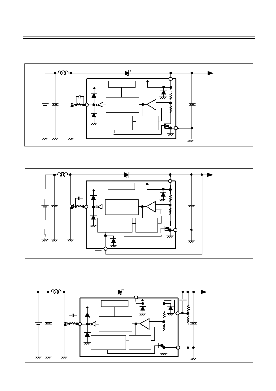
Block Diagram
(1) S-8357/58 Series B, H, F Type
(
Without shutdown function
)
(2) S-8357/58 Series B, H, F, N Type (
With shutdown function
)
Figure 1
Figure 2
(3) S-8357/58 Series E, J, G, P Type
(
V
DD
/V
OUT
separate type
)
(4) S-8355/56 Series K, L, M, Q Type
Figure 3
Figure 4
-
+
EXT
VOUT
VSS
VDD
IC internal
power
supply
PWM or PWM
/PFM switching
control circuit
Phase
compensation
circuit
Soft start
built-in reference
power supply
Oscillation
Circuit
-
+
Soft start
built-in reference
power supply
IC internal
power
supply
VOUT
EXT
VSS
Phase
compensation
circuit
VDD
Oscillation
Circuit
ON/OFF
PWM or PWM
/PFM switching
control circuit
-
+
IC internal
power supply
VOUT
EXT
VSS
PWM or PWM
/PFM switching
control circuit
Soft start
built-in reference
power supply
Phase
compensation
circuit
Oscillation
Circuit
-
+
IC internal
power supply
VOUT
VSS
PWM or PWM
/PFM switching
control circuit
Soft start
built-in reference
power supply
EXT
Oscillation
Circuit
ON/OFF
Phase
compensation
circuit
SUPER-SMALL PACKAGE PWM CONTROL, PWM/PFM SWITCHING CONTROL STEP-UP SWITCHING REGULATOR
Rev.4.1
_00
S-8355/56/57/58 Series
Seiko Instruments Inc.
3
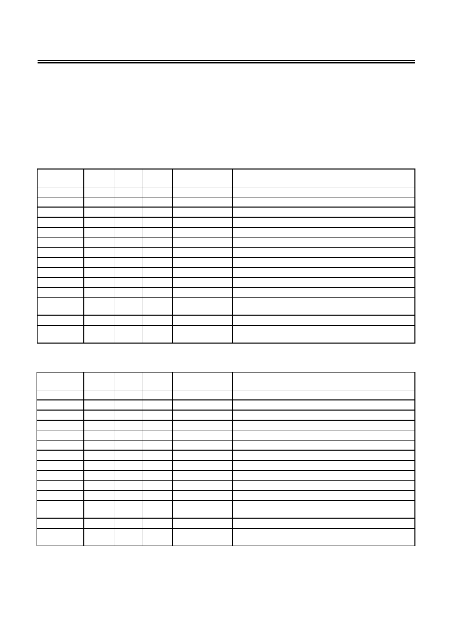
Selection Guide
∑ The control types, product types, output voltage, and packages for the S-8355/56/57/58 Series can be
selected at the user's request. Please refer to the "Product name selection guide" for the definition of
the product name and "Product Name List" for the full product names.
1. Function List
1-1. PWM control products
Table 1
Product Name
Switching
Frequency
(kHz)
Shutdown
Function
V
DD
/V
OUT
Separate
Type
Package Application
S-8355KxxMC
100
Yes
Yes
SOT-23-5
Applications requiring variable output voltage and a shutdown function
S-8355LxxMC/BD
250
Yes
Yes
SOT-23-5/6-Pin SNB(B)
Applications requiring variable output voltage, a shutdown function, and a thin coil
S-8355MxxMC/BD
300
Yes
Yes
SOT-23-5/6 Pin-SNB(B)
Applications requiring variable output voltage, a shutdown function, and a thin coil
S-8355QxxMC/BD
600
Yes
Yes
SOT-23-5/6-Pin SNB(B)
Applications requiring variable output voltage, a shutdown function, and a thin coil
S-8357BxxMC 100 Yes
SOT-23-5
Applications requiring a shutdown function
S-8357BxxMA 100
SOT-23-3
Applications not requiring a shutdown function
S-8357BxxUA 100
SOT-89-3
Applications not requiring a shutdown function
S-8357ExxMC 100
Yes
SOT-23-5
Applications in which output voltage is adjusted by external resistor
S-8357FxxMC/BD 300
Yes
SOT-23-5/6-Pin SNB(B)
Applications requiring a shutdown function and a thin coil
S-8357GxxMC/BD 300
Yes
SOT-23-5/6-Pin SNB(B)
Applications requiring variable output voltage and a thin coil
S-8357HxxMC/BD 250
Yes
SOT-23-5/6-Pin SNB(B)
Applications requiring a shutdown function and a thin coil
S-8357JxxMC/BD 250
Yes
SOT-23-5/6-Pin
SNB(B)
Applications requiring variable output voltage with an external resistor and a thin
coil
S-8357NxxMC/BD 600
Yes
SOT-23-5/6-Pin SNB(B)
Applications requiring a shutdown function and a thin coil
S-8357PxxMC/BD 600
Yes
SOT-23-5/6-Pin
SNB(B)
Applications requiring variable output voltage with an external resistor and a thin
coil
1-2. PWM/PFM switching control products
Table 2
Product name
Switching
Frequency
(kHz)
Shutdown
Function
V
DD
/V
OUT
Separate
Type
Package Application
S-8356KxxMC
100
Yes
Yes
SOT-23-5
Applications requiring variable output voltage and a shutdown function
S-8356LxxMC/BD
250
Yes
Yes
SOT-23-5/6-Pin SNB(B)
Applications requiring variable output voltage, a shutdown function, and a thin coil
S-8356MxxMC/BD
300
Yes
Yes
SOT-23-5/6-Pin SNB(B)
Applications requiring variable output voltage, a shutdown function, and a thin coil
S-8356QxxMC/BD
600
Yes
Yes
SOT-23-5/6-Pin SNB(B)
Applications requiring variable output voltage, a shutdown function, and a thin coil
S-8358BxxMC 100 Yes
SOT-23-5
Applications requiring a shutdown function
S-8358BxxMA 100
SOT-23-3
Applications not requiring a shutdown function
S-8358BxxUA 100
SOT-89-3
Applications not requiring a shutdown function
S-8358ExxMC 100
Yes
SOT-23-5
Applications in which output voltage is adjusted by external resistor
S-8358FxxMC/BD 300 Yes
SOT-23-5/6-Pin SNB(B)
Applications requiring a shutdown function and a thin coil
S-8358GxxMC/BD 300
Yes
SOT-23-5/6-Pin SNB(B)
Applications requiring variable output voltage and a thin coil
S-8358HxxMC/BD 250
Yes
SOT-23-5/6-Pin SNB(B)
Applications requiring a shutdown function and a thin coil
S-8358JxxMC/BD 250
Yes
SOT-23-5/6-Pin
SNB(B)
Applications requiring variable output voltage with an external resistor and a thin
coil
S-8358NxxMC/BD 600
Yes
SOT-23-5/6-Pin SNB(B)
Applications requiring a shutdown function and a thin coil
S-8358PxxMC/BD 600
Yes
SOT-23-5/6-Pin
SNB(B)
Applications requiring variable output voltage with an external resistor and a thin
coil

SUPER-SMALL PACKAGE PWM CONTROL, PWM/PFM SWITCHING CONTROL STEP-UP SWITCHING REGULATOR
S-8355/56/57/58 Series
Rev.4.1
_00
4
Seiko Instruments Inc.
2. Package and Function List by Product Type
Table 3
Series Name
Type
Package Name
(Abbreviation)
Shutdown
Function
Yes/No
V
DD
/V
OUT
Separate Type
Yes/No
S-8355 Series
S-8356 Series
K, L, M, Q
(Shutdown function
+ V
DD
/V
OUT
separate type)
K
= 100 kHz, L = 250 kHz, M = 300 kHz, Q = 600 kHz
MC/BD Yes Yes
MA/UA No
B, H, F
(Normal product)
B
= 100 kHz, H = 250 kHz, F = 300 kHz
MC/BD Yes
No
N
(Normal product)
N
= 600 kHz
MC/BD Yes No
S-8357 Series
E, J, G, P
(V
DD
/V
OUT
separate type)
E
= 100 kHz, J = 250 kHz, G = 300 kHz, P = 600 kHz
MC/BD No Yes
MA/UA No
B, H, F
(Normal product)
B
= 100 kHz, H = 250 kHz, F = 300 kHz
MC/BD Yes
No
N
(Normal product)
N
= 600 kHz
MC/BD Yes No
S-8358 Series
E, J, G, P
(V
DD
/V
OUT
separate type)
E
= 100 kHz, J = 250 kHz, G = 300 kHz, P = 600 kHz
MC/BD No Yes
SUPER-SMALL PACKAGE PWM CONTROL, PWM/PFM SWITCHING CONTROL STEP-UP SWITCHING REGULATOR
Rev.4.1
_00
S-8355/56/57/58 Series
Seiko Instruments Inc.
5
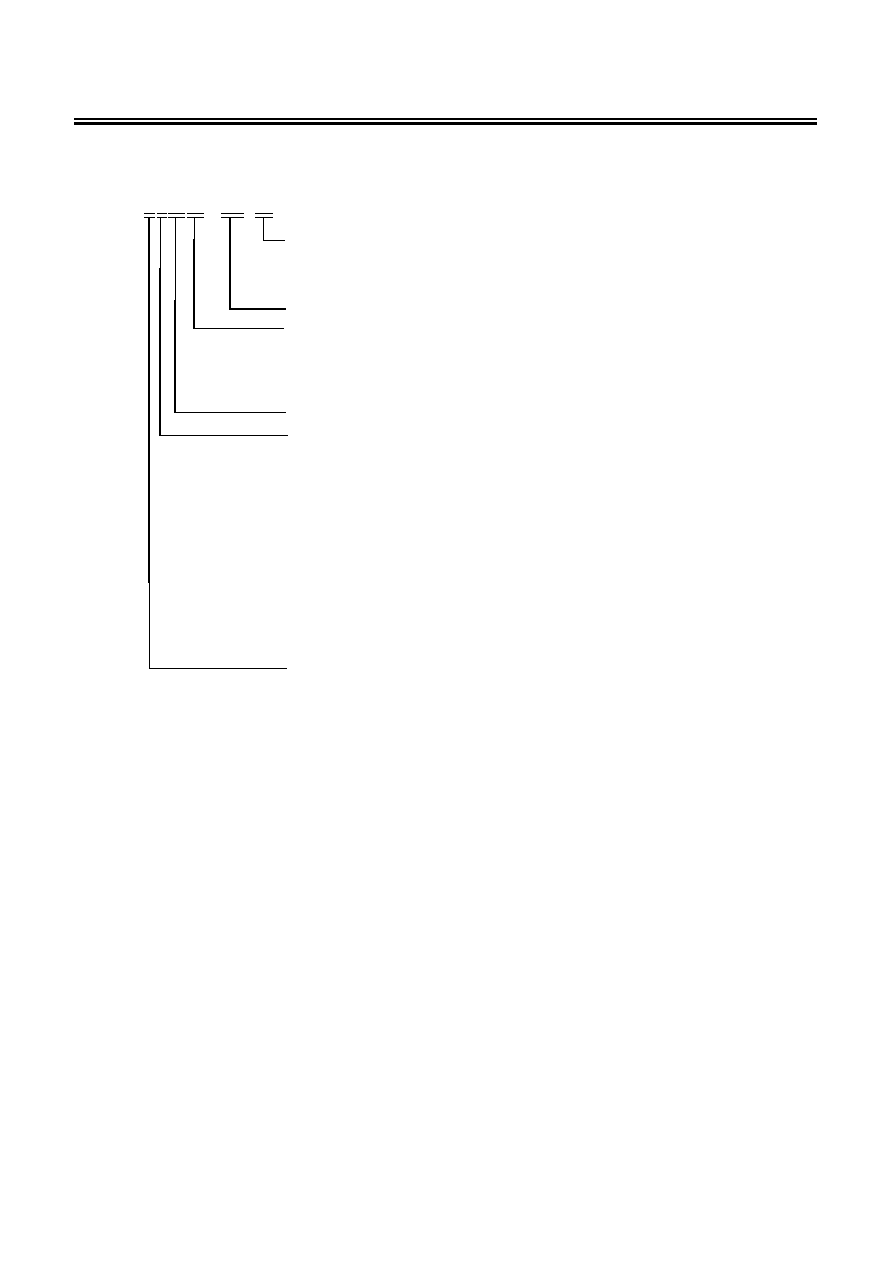
3.
Product Name
S-835 x x xx xx - xxx - Tx
IC direction in tape specifications
*1
T2: SOT-89-3, SOT-23-3, SOT-23-5
TF: 6-Pin SNB(B)
Product name (abbreviation)
*2
Package name (abbreviation)
UA:
SOT-89-3
MA:
SOT-23-3
MC:
SOT-23-5
BD:
6-Pin-SNB(B)
Output voltage 15 to 65 (Ex. When the output voltage is 1.5 V, it is expressed as 15.)
Product type
B:
Normal
product,
f
OSC
= 100 kHz (S-8357/58)
H:
Normal
product,
f
OSC
= 250 kHz (S-8357/58)
F: Normal product,
f
OSC
= 300 kHz (S-8357/58)
N:
Normal
product,
f
OSC
= 600 kHz (S-8357/58)
E:
V
DD
/V
OUT
separate type,
f
OSC
= 100 kHz (S-8357/58)
J:
V
DD
/V
OUT
separate type,
f
OSC
= 250 kHz (S-8357/58)
G:
V
DD
/V
OUT
separate type,
f
OSC
= 300 kHz (S-8357/58)
P:
V
DD
/V
OUT
separate type,
f
OSC
= 600 kHz (S-8357/58)
K:
Shutdown
function
+ V
DD
/V
OUT
separate type, f
OSC
= 100 kHz (S-8355/56)
L: Shutdown function
+ V
DD
/V
OUT
separate type, f
OSC
= 250 kHz (S-8355/56)
M:
Shutdown
function
+ V
DD
/V
OUT
separate type, f
OSC
= 300 kHz (S-8355/56)
Q:
Shutdown
function
+ V
DD
/V
OUT
separate type, f
OSC
= 600 kHz (S-8355/56)
Control system
5 or 7: PWM control
6 or 8: PWM/PFM switching control
*1. Please refer to the taping specifications at the end of this document.
*2. Please refer to the product name list.

SUPER-SMALL PACKAGE PWM CONTROL, PWM/PFM SWITCHING CONTROL STEP-UP SWITCHING REGULATOR
S-8355/56/57/58 Series
Rev.4.1
_00
6
Seiko Instruments Inc.
4. Product Name List
4-1. S-8355 Series
Table 4
Model
Output Voltage
S-8355KxxMC Series
S-8355LxxMC Series
S-8355MxxMC Series
S-8355MxxBD Series
S-8355QxxBD Series
1.5 V
S-8355Q15BD-OWA-TF
1.8 V
S-8355K18MC-NAD-T2
S-8355M18MC-MCD-T2
S-8355M18BD-MCD-TF
2.0 V
S-8355K20MC-NAF-T2
S-8355L20MC-NCF-T2
S-8355M20MC-MCF-T2
3.1 V
S-8355K31MC-NAQ-T2
S-8355M31MC-MCQ-T2
3.3 V
S-8355K33MC-NAS-T2
3.4 V
S-8355M34MC-MCT-T2
5.0 V
S-8355K50MC-NBJ-T2
S-8355M50MC-MDJ-T2
5.5 V
S-8355M55MC-MDO-T2
Remark Please consult our sales person for products with an output voltage other than those specified above.
4-2. S-8356 Series
Table 5
Model
Output Voltage
S-8356KxxMC Series
S-8356MxxMC Series
S-8355MxxBD Series
S-8356QxxMC Series
1.8 V
S-8356K18MC-NED-T2
S-8356M18MC-MED-T2
S-8356M18BD-MED-TF
3.0 V
S-8356M30MC-MEP-T2
3.3 V
S-8356K33MC-NES-T2
S-8356Q33MC-OYS-T2
5.0 V
S-8356K50MC-NFJ-T2
S-8356M50MC-MFJ-T2
S-8356Q50MC-OVJ-T2
Remark Please consult our sales person for products with an output voltage other than those
specified above.
4-3. S-8357 Series (1)
Table 6
Model
Output Voltage
S-8357BxxMC Series
S-8357BxxMA Series
S-8357BxxUA Series
S-8357ExxMC Series
S-8357FxxMC Series
2.0 V
S-8357E20MC-NKF-T2
2.5 V
2.6 V
S-8357B26MC-NIL-T2
3.0 V
S-8357B30MC-NIP-T2
S-8357B30MA-NIP-T2
3.1 V
3.2 V
S-8357F32MC-MGR-T2
3.3 V
S-8357B33MC-NIS-T2
S-8357B33MA-NIS-T2
S-8357B33UA-NIS-T2
S-8357F33MC-MGS-T2
3.5 V
3.6 V
S-8357B36MC-NIV-T2
4.8 V
S-8357B48MC-NJH-T2
S-8357B48UA-NJH-T2
5.0 V
S-8357B50MC-NJJ-T2
S-8357B50MA-NJJ-T2
S-8357B50UA-NJJ-T2
S-8357E50MC-NLJ-T2
S-8357F50MC-MHJ-T2
5.2 V
S-8357B52MC-NJL-T2
5.4 V
S-8357B54MC-NJN-T2
6.0 V
S-8357B60MC-NJT-T2
Remark Please consult our sales person for products with an output voltage other than those specified above.

SUPER-SMALL PACKAGE PWM CONTROL, PWM/PFM SWITCHING CONTROL STEP-UP SWITCHING REGULATOR
Rev.4.1
_00
S-8355/56/57/58 Series
Seiko Instruments Inc.
7
4-4. S-8357 Series (2)
Table
7
Model
Output Voltage
S-8357GxxMC Series
S-8357HxxMC Series
S-8357JxxMC Series
S-8357NxxMC Series
2.0 V
2.5 V
S-8357J25MC-NOK-T2
2.6 V
3.0 V
3.1 V
S-8357H31MC-NMQ-T2
3.2 V
3.3 V
S-8357N33MC-O2S-T2
3.5 V
S-8357H35MC-NMU-T2
3.6 V
S-8357H36MC-NMV-T2
4.8 V
5.0 V
S-8357G50MC-MJJ-T2
S-8357J50MC-NPJ-T2
S-8357N50MC-O3J-T2
5.2 V
5.4 V
6.0 V
Remark
Please consult our sales person for products with an output voltage other than those
specified
above.
4-5. S-8358 Series (1)
Table 8
Model
Output Voltage
S-8358BxxMC Series
S-8358BxxMA Series
S-8358BxxUA Series
S-8358ExxMC Series
S-8358FxxMC Series
2.0 V
S-8358E20MC-NSF-T2
2.5 V
S-8358B25MC-NQK-T2
2.6 V
S-8358B26MC-NQL-T2
3.0 V
S-8358B30MC-NQP-T2
3.1 V
S-8358B31MC-NQQ-T2
3.2 V
S-8357B32MC-NQR-T2
3.3 V
S-8358B33MC-NQS-T2
S-8358B33UA-NQS-T2 S-8358F33MC-MKS-T2
3.5 V
S-8358B35MC-NQU-T2
3.6 V
S-8358B36MC-NQV-T2
3.8 V
S-8358B38MC-NQX-T2
5.0 V
S-8358B50MC-NRJ-T2
S-8358B50MA-NRJ-T2
S-8358B50UA-NRJ-T2
S-8358E50MC-NTJ-T2
S-8358F50MC-MLJ-T2
5.3 V
S-8358F53MC-MLM-T2
6.0 V
S-8358B60MC-NRT-T2
Remark
Please consult our sales person for products with an output voltage other than those specified above.
4-6. S-8358 Series (2)
Table
9
Model
Output Voltage
S-8357GxxMC Series
S-8357HxxMC Series
S-8358JxxMC Series
2.0 V
2.5 V
2.6 V
3.0 V
S-8358H30MC-NUP-T2
3.1 V
3.2 V
3.3 V
S-8358H33MC-NUS-T2
S-8358J33MC-NWS-T2
3.5 V
3.6 V
3.8 V
5.0 V
S-8358G50MC-MNJ-T2
S-8358H50MC-NVJ-T2
S-8358J50MC-NXJ-T2
5.3 V
6.0 V
Remark
Please consult our sales person for products with an output
voltage other than those specified above.

SUPER-SMALL PACKAGE PWM CONTROL, PWM/PFM SWITCHING CONTROL STEP-UP SWITCHING REGULATOR
S-8355/56/57/58 Series
Rev.4.1
_00
8
Seiko Instruments Inc.
Pin Assignment
Table 10
Products: S-8357/58 Series B, H, F Types
(Without shutdown function, V
DD
/V
OUT
non-separate type)
Pin No.
Pin Name
Functions
1 VSS
GND
pin
2
VOUT
Output voltage pin and IC power supply pin
3
EXT
External transistor connection pin
Table 11
Products: S-8357/58 Series B, H, F Types
(Without shutdown function, V
DD
/V
OUT
non-separate type)
Pin No.
Pin Name
Functions
1
VOUT
Output voltage pin and IC power supply pin
2 VSS
GND
pin
3
EXT
External transistor connection pin
SOT-89-3
Top view
3
2
1
Figure 5
Figure 6
3
2
1
SOT23-3
Top view

SUPER-SMALL PACKAGE PWM CONTROL, PWM/PFM SWITCHING CONTROL STEP-UP SWITCHING REGULATOR
Rev.4.1
_00
S-8355/56/57/58 Series
Seiko Instruments Inc.
9
Table 12
Products: S-8355/56 Series K, L, M, Q Types
(With shutdown function, V
DD
/V
OUT
separate type)
Pin No.
Pin Name
Functions
1
VOUT
Output voltage pin
2
VDD
IC power supply pin
3 ON/OFF
Shutdown pin
"H": Normal operation (Step-up operation)
"L": Stop step-up (Whole circuit stop)
4 VSS
GND
pin
5
EXT
External transistor connection pin
Table 13
Products: S-8357/58 Series B, H, F, N Types
(With shutdown function, V
DD
/V
OUT
non-separate type)
Pin No.
Pin Name
Functions
1 ON/OFF
Shutdown pin
"H": Normal operation (Step-up operation)
"L": Stop step-up (Whole circuit stop)
2
VOUT
Output voltage pin and IC power supply pin
3
NC
*1
No connection
4 VSS
GND
pin
5
EXT
External transistor connection pin
*1. The NC pin indicates electrically open.
Table 14
Products: S-8357/58 Series E, J, G, P Types
(Without shutdown function, V
DD
/V
OUT
separate type)
Pin No.
Pin Name
Functions
1
VOUT
Output voltage pin
2
VDD
IC power supply pin
3
NC
*1
No connection
4 VSS
GND
pin
5
EXT
External transistor connection pin
*1. The NC pin indicates electrically open.
SOT23-5
Top view
3
2
1
5
4
Figure 7

SUPER-SMALL PACKAGE PWM CONTROL, PWM/PFM SWITCHING CONTROL STEP-UP SWITCHING REGULATOR
S-8355/56/57/58 Series
Rev.4.1
_00
10
Seiko Instruments Inc.
Table 15
Products: S-8355/56 Series K, L, M, Q Types
(With shutdown function, V
DD
/V
OUT
separate type)
Pin No.
Pin Name
Functions
1 ON/OFF
Shutdown pin
"H": Normal operation (Step-up operation)
"L": Stop step-up (Whole circuit stop)
2
VOUT
Output voltage pin
3
VDD
IC power supply pin
4
EXT
External transistor connection pin
5
NC
*1
No connection
6 VSS
GND
pin
*1. The NC pin indicates electrically open.
Table 16
Products: S-8357/58 Series B, H, F, N Types
(With shutdown function, V
DD
/V
OUT
non-separate type)
Pin No.
Pin Name
Functions
1
NC
*1
No connection
2 ON/OFF
Shutdown pin
"H": Normal operation (Step-up operation)
"L": Stop step-up (Whole circuit stop)
3
VOUT
Output voltage pin and IC power supply pin
4
EXT
External transistor connection pin
5
NC
*1
No connection
6 VSS
GND
pin
*1. The NC pin indicates electrically open.
Table 17
Products: S-8357/58 Series E, J, G, P Types
(Without shutdown function, V
DD
/V
OUT
separate type)
Pin No.
Pin Name
Functions
1
NC
*1
No connection
2
VOUT
Output voltage pin
3
VDD
IC power supply pin
4
EXT
External transistor connection pin
5
NC
*1
No connection
6 VSS
GND
pin
*1. The NC pin indicates electrically open.
6-Pin SNB(B)
Top view
3
2
1
6
4
5
Figure 8
SUPER-SMALL PACKAGE PWM CONTROL, PWM/PFM SWITCHING CONTROL STEP-UP SWITCHING REGULATOR
Rev.4.1
_00
S-8355/56/57/58 Series
Seiko Instruments Inc.
11
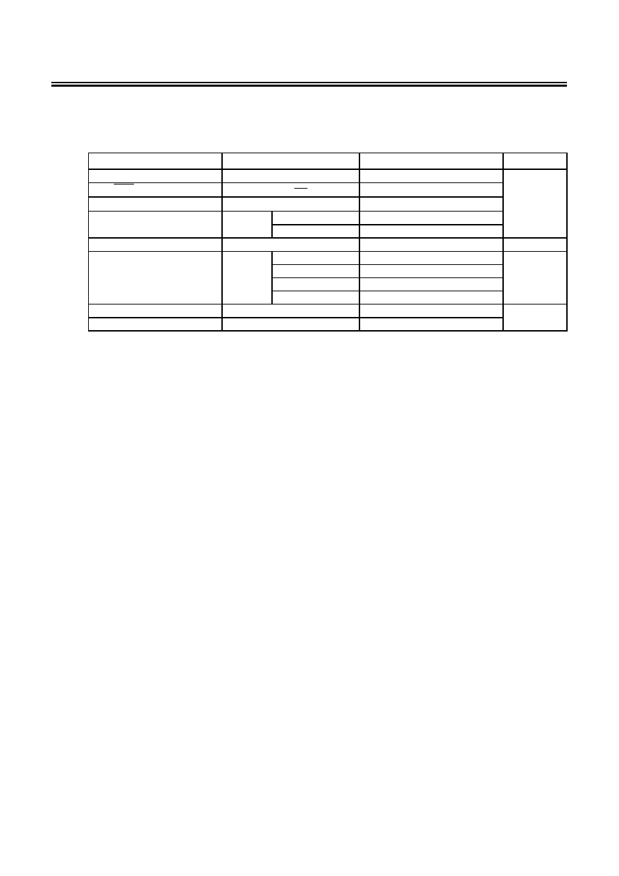
Absolute Maximum Ratings
Table 18
(Unless otherwise specified: Ta
= 25įC)
Parameter Symbol
Ratings
Unit
VOUT pin voltage
V
OUT
V
SS
- 0.3 to V
SS
+ 12
ON/OFF pin voltage
*1
V
ON/OFF
V
SS
- 0.3 to V
SS
+ 12
VDD pin voltage
*2
V
DD
V
SS
- 0.3 to V
SS
+ 12
B, H, F, N type
V
SS
- 0.3 to V
OUT
+ 0.3
EXT pin voltage
V
EXT
Others
V
SS
- 0.3 to V
DD
+ 0.3
V
EXT pin current
I
EXT
Ī80
mA
SOT-89-3 500
SOT-23-3 150
SOT-23-5 250
Power dissipation
P
D
6-Pin SNB(B)
90
mW
Operating temperature
Topr
-40 to +85
Storage temperature
Tstg
-40 to +125
įC
*1. With shutdown function
*2. For V
DD
/V
OUT
separate types
Caution The absolute maximum ratings are rated values exceeding which the product could suffer physical
damage. These values must therefore not be exceeded under any conditions.
SUPER-SMALL PACKAGE PWM CONTROL, PWM/PFM SWITCHING CONTROL STEP-UP SWITCHING REGULATOR
S-8355/56/57/58 Series
Rev.4.1
_00
12
Seiko Instruments Inc.
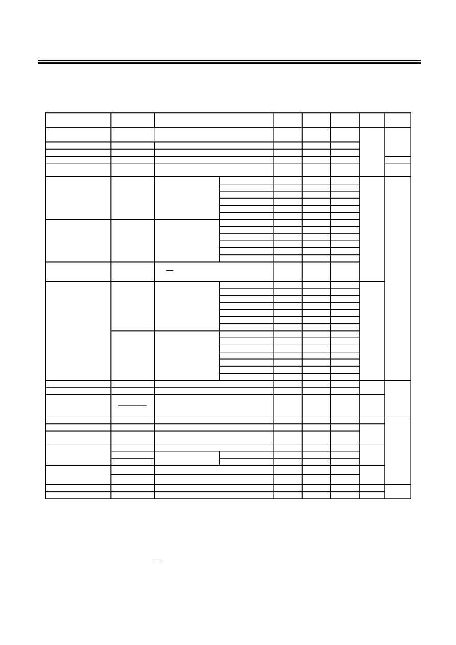
Electrical Characteristics
(1) 100 kHz types (S-835xBxx, S-835xExx, S-835xKxx)
Table 19
(Unless otherwise specified: Ta
= 25įC)
Parameter Symbol
Conditions
Min.
Typ.
Max.
Unit
Test
Circuit
Output voltage
V
OUT
V
OUT(S)
◊ 0.976
V
OUT(S)
V
OUT(S)
◊ 1.024
V 2
Input voltage
V
IN
-
-
10
Operation start voltage
V
ST1
I
OUT
= 1 mA
-
-
0.9
Oscillation start voltage
V
ST2
No external parts, voltage applied to V
OUT
-
-
0.8
1
Operation holding
voltage
V
HLD
I
OUT
= 1 mA, Measured by decreasing V
IN
voltage
gradually
0.7
-
-
2
S-835xx15 to 19
-
14.0 23.4
S-835xx20 to 29
-
19.7 32.9
S-835xx30 to 39
-
25.9 43.2
S-835xx40 to 49
-
32.6 54.4
S-835xx50 to 59
-
39.8 66.4
Current consumption 1
I
SS1
V
OUT
= V
OUT(S)
◊ 0.95
S-835xx60 to 65
-
47.3 78.9
S-835xx15 to 19
-
5.6 11.1
S-835xx20 to 29
-
5.8 11.5
S-835xx30 to 39
-
5.9 11.8
S-835xx40 to 49
-
6.1 12.1
S-835xx50 to 59
-
6.3 12.5
Current consumption 2
I
SS2
V
OUT
= V
OUT(S)
+ 0.5
S-835xx60 to 65
-
6.4 12.8
Current consumption
during shutdown
(with shutdown function)
I
SSS
V
ON/OFF
= 0 V
-
-
0.5
ĶA
S-835xx15 to 19
-4.5
-8.9
-
S-835xx20 to 24
-6.2
-12.3
-
S-835xx25 to 29
-7.8
-15.7
-
S-835xx30 to 39
-10.3
-20.7
-
S-835xx40 to 49
-13.3
-26.7
-
S-835xx50 to 59
-16.1
-32.3
-
I
EXTH
V
EXT
= V
OUT
- 0.4
S-835xx60 to 65
-18.9
-37.7
-
S-835xx15 to 19
9.5
19.0
-
S-835xx20 to 24
12.6
25.2
-
S-835xx25 to 29
15.5
31.0
-
S-835xx30 to 39
19.2
38.5
-
S-835xx40 to 49
23.8
47.6
-
S-835xx50 to 59
27.4
54.8
-
EXT pin output current
I
EXTL
V
EXT
= 0.4 V
S-835xx60 to 65
30.3
60.6
-
mA
1
Line regulation
V
OUT1
V
IN
= V
OUT(S)
◊ 0.4 to ◊ 0.6
-
30 60
Load regulation
V
OUT2
I
OUT
= 10 ĶA to V
OUT(S)
/50
◊ 1.25
-
30 60
mV
Output voltage
temperature coefficient
V
O U T
Ta ∑ V
O U T
Ta
= -40įC to +85įC
-
Ī50
- ppm/įC
2
Oscillation frequency
f
OSC
V
OUT
= V
OUT(S)
◊ 0.95
85
100
115
kHz
Max. duty ratio
MaxDuty
V
OUT
= V
OUT(S)
◊ 0.95
75
83
90
PWM/PFM switching
duty ratio (S-8356/58)
PFMDuty
V
IN
= V
OUT(S)
- 0.1 V, no load
10 15 24
%
V
SH
Measured the oscillation at EXT pin
0.75
-
-
V
SL1
When V
OUT
1.5 V
-
-
0.3
Shutdown pin input
voltage (with shutdown
function)
V
SL2
Judged the stop of
oscillation at EXT pin
When V
OUT
< 1.5 V
-
-
0.2
V
I
SH
Shutdown pin
= V
OUT(S)
◊ 0.95
-0.1
-
0.1
Shutdown pin input
current (with shutdown
function)
I
SL
Shutdown pin
= 0 V
-0.1
-
0.1
ĶA
1
Soft start time
t
SS
3.0 6.0 12.0 ms
Efficiency EFFI
-
86
-
%
2
External parts
- Coil:
CDRH6D28-470 of Sumida Corporation
- Diode:
RB461F (Schottky type) of Rohm Co., Ltd.
- Capacitor:
F93 (16 V, 47
ĶF tantalum type) of Nichicon Corporation
- Transistor :
CPH3210 of Sanyo Electric Co., Ltd.
- Base resistor (R
b
): 1.0 k
- Base capacitor (C
b
): 2200 pF (ceramic type)
V
IN
= V
OUT(S)
◊ 0.6 applied, I
OUT
= V
OUT(S)
/50
Shutdown function built-in type: ON/OFF pin is connected to V
OUT
V
DD
/V
OUT
separate type:
VDD pin is connected to VOUT pin
Remarks 1. V
OUT(S)
specified above is the set output voltage value, and V
OUT
is the typical value of the output voltage.
2. V
DD
/V
OUT
separate type:
Step-up operation is performed from V
DD
= 0.8 V.
However, 1.8
V
DD
10 V is recommended to stabilize the output voltage and oscillation frequency.
(V
DD
1.8 V must be applied for products with a set value of less than 1.9 V.)

SUPER-SMALL PACKAGE PWM CONTROL, PWM/PFM SWITCHING CONTROL STEP-UP SWITCHING REGULATOR
Rev.4.1
_00
S-8355/56/57/58 Series
Seiko Instruments Inc.
13
(2) 250 kHz types (S-835xHxx, S-835xJxx, S-835xLxx)
Table 20
(Unless otherwise specified: Ta
= 25įC)
Parameter Symbol
Conditions
Min.
Typ.
Max.
Unit
Test
Circuit
Output voltage
V
OUT
V
OUT(S)
◊ 0.976
V
OUT(S)
V
OUT(S)
◊ 1.024
V 2
Input voltage
V
IN
-
-
10
Operation start voltage
V
ST1
I
OUT
= 1 mA
-
-
0.9
Oscillation start voltage
V
ST2
No external parts,
voltage applied to
V
OUT
-
-
0.8 1
Operation holding
voltage
V
HLD
I
OUT
= 1 mA,
Measured by decreasing
V
IN
voltage
gradually
0.7
-
-
2
S-835xx15 to 19
-
28.9 48.2
S-835xx20 to 29
-
42.7 71.1
S-835xx30 to 39
-
58.0 96.7
S-835xx40 to 49
-
74.5 124.1
S-835xx50 to 59
-
92.0 153.4
Current consumption
1 I
SS1
V
OUT
= V
OUT(S)
◊ 0.95
S-835xx60 to 65
-
110.5 184.2
S-835xx15 to 19
-
8.7 17.3
S-835xx20 to 29
-
8.8 17.6
S-835xx30 to 39
-
9.0 18.0
S-835xx40 to 49
-
9.2 18.3
S-835xx50 to 59
-
9.3 18.6
Current consumption
2 I
SS2
V
OUT
= V
OUT(S)
+ 0.5
S-835xx60 to 65
-
9.5 19.0
Current consumption
during shutdown
(with shutdown function)
I
SSS
V
ON/OFF
= 0 V
-
-
0.5
ĶA
S-835xx15 to 19
-4.5
-8.9
-
S-835xx20 to 24
-6.2
-12.3
-
S-835xx25 to 29
-7.8
-15.7
-
S-835xx30 to 39
-10.3
-20.7
-
S-835xx40 to 49
-13.3
-26.7
-
S-835xx50 to 59
-16.1
-32.3
-
I
EXTH
V
EXT
= V
OUT
- 0.4
S-835xx60 to 65
-18.9
-37.7
-
S-835xx15 to 19
9.5
19.0
-
S-835xx20 to 24
12.6
25.2
-
S-835xx25 to 29
15.5
31.0
-
S-835xx30 to 39
19.2
38.5
-
S-835xx40 to 49
23.8
47.6
-
S-835xx50 to 59
27.4
54.8
-
EXT pin output current
I
EXTL
V
EXT
= 0.4 V
S-835xx60 to 65
30.3
60.6
-
mA
1
Line regulation
V
OUT1
V
IN
= V
OUT(S)
◊ 0.4 to ◊ 0.6
-
30 60
Load regulation
V
OUT2
I
OUT
= 10 ĶA to V
OUT(S)
/50
◊ 1.25
-
30 60
mV
Output voltage
temperature coefficient
V
O U T
Ta ∑ V
O U T
Ta
= -40įC to +85įC
-
Ī50
- ppm/įC
2
Oscillation frequency
f
OSC
V
OUT
= V
OUT(S)
◊ 0.95
212.5 250 287.5 kHz
Max. duty ratio
MaxDuty
V
OUT
= V
OUT(S)
◊ 0.95
70 78 85
PWM/PFM switching
duty ratio (S-8356/58)
PFMDuty
V
IN
= V
OUT(S)
- 0.1 V, no load
10 15 24
%
V
SH
Measured the oscillation at EXT pin
0.75
-
-
V
SL1
When V
OUT
1.5 V
-
-
0.3
Shutdown pin input
voltage (with shutdown
function)
V
SL2
Judged the stop of
oscillation at EXT pin
When V
OUT
< 1.5 V
-
-
0.2
V
I
SH
Shutdown pin
= V
OUT(S)
◊ 0.95
-0.1
-
0.1
Shutdown pin input
current (with shutdown
function)
I
SL
Shutdown pin
= 0 V
-0.1
-
0.1
ĶA
1
Soft start time
t
SS
1.5 3.0 6.0 ms
Efficiency EFFI
-
85
-
%
2
External parts
- Coil:
CDRH6D28-220 of Sumida Corporation
- Diode:
RB461F (Schottky type) of Rohm Co., Ltd.
- Capacitor:
F93 (16 V, 47
ĶF tantalum type) of Nichicon Corporation
- Transistor :
CPH3210 of Sanyo Electric Co., Ltd.
- Base resistor (R
b
): 1.0 k
- Base capacitor (C
b
): 2200 pF (ceramic type)
V
IN
= V
OUT(S)
◊ 0.6 applied, I
OUT
= V
OUT(S)
/50
Shutdown function built-in type: ON/OFF pin is connected to V
OUT
V
DD
/V
OUT
separate type:
VDD pin is connected to VOUT pin
Remarks 1. V
OUT(S)
specified above is the set output voltage value, and V
OUT
is the typical value of the output voltage.
2. V
DD
/V
OUT
separate type:
Step-up operation is performed from V
DD
= 0.8 V.
However,
1.8
V
DD
10 V is recommended to stabilize the output voltage and oscillation frequency.
(V
DD
1.8 V must be applied for products with a set value of less than 1.9 V.)

SUPER-SMALL PACKAGE PWM CONTROL, PWM/PFM SWITCHING CONTROL STEP-UP SWITCHING REGULATOR
S-8355/56/57/58 Series
Rev.4.1
_00
14
Seiko Instruments Inc.
(3) 300 kHz types (S-835xFxx, S-835xGxx, S-835xMxx)
Table 21
(Unless otherwise specified: Ta
= 25įC)
Parameter Symbol
Conditions
Min.
Typ.
Max.
Unit
Test
Circuit
Output voltage
V
OUT
V
OUT(S)
◊ 0.976
V
OUT(S)
V
OUT(S)
◊ 1.024
V 2
Input voltage
V
IN
-
-
10
Operation start voltage
V
ST1
I
OUT
= 1 mA
-
-
0.9
Oscillation start voltage
V
ST2
No external parts, voltage applied to
V
OUT
-
-
0.8
1
Operation holding
voltage
V
HLD
I
OUT
= 1 mA,
Measured by decreasing
V
IN
voltage
gradually
0.7
-
-
2
S-835xx15 to 19
-
33.8 56.4
S-835xx20 to 29
-
50.3 83.9
S-835xx30 to 39
-
68.6 114.4
S-835xx40 to 49
-
88.4 147.4
S-835xx50 to 59
-
109.4 182.4
Current consumption 1
I
SS1
V
OUT
= V
OUT(S)
◊ 0.95
S-835xx60 to 65
-
131.6 219.3
S-835xx15 to 19
-
9.7 19.4
S-835xx20 to 29
-
9.9 19.7
S-835xx30 to 39
-
10.0 20.0
S-835xx40 to 49
-
10.2 20.4
S-835xx50 to 59
-
10.4 20.7
Current consumption 2
I
SS2
V
OUT
= V
OUT(S)
+ 0.5
S-835xx60 to 65
-
10.5 21.0
Current consumption
during shutdown
(with shutdown function)
I
SSS
V
ON/OFF
= 0 V
-
-
0.5
ĶA
S-835xx15 to 19
-4.5
-8.9
-
S-835xx20 to 24
-6.2
-12.3
-
S-835xx25 to 29
-7.8
-15.7
-
S-835xx30 to 39
-10.3
-20.7
-
S-835xx40 to 49
-13.3
-26.7
-
S-835xx50 to 59
-16.1
-32.3
-
I
EXTH
V
EXT
= V
OUT
- 0.4
S-835xx60 to 65
-18.9
-37.7
-
S-835xx15 to 19
9.5
19.0
-
S-835xx20 to 24
12.6
25.2
-
S-835xx25 to 29
15.5
31.0
-
S-835xx30 to 39
19.2
38.5
-
S-835xx40 to 49
23.8
47.6
-
S-835xx50 to 59
27.4
54.8
-
EXT pin output current
I
EXTL
V
EXT
= 0.4 V
S-835xx60 to 65
30.3
60.6
-
mA
1
Line regulation
V
OUT1
V
IN
= V
OUT(S)
◊ 0.4 to ◊ 0.6
-
30 60
Load regulation
V
OUT2
I
OUT
= 10 ĶA to V
OUT(S)
/50
◊ 1.25
-
30 60
mV
Output voltage
temperature coefficient
V
O U T
Ta ∑ V
O U T
Ta
= - 40įC to + 85įC
-
Ī50
- ppm/įC
2
Oscillation frequency
f
OSC
V
OUT
= V
OUT(S)
◊ 0.95
255 300 345 kHz
Max. duty ratio
MaxDuty
V
OUT
= V
OUT(S)
◊ 0.95
70 78 85
PWM/PFM switching
duty ratio (S-8356/58)
PFMDuty
V
IN
= V
OUT(S)
- 0.1 V, no load
10 15 24
%
V
SH
Measured the oscillation at EXT pin
0.75
-
-
V
SL1
When V
OUT
1.5 V
-
-
0.3
Shutdown pin input
voltage (with shutdown
function)
V
SL2
Judged the stop of
oscillation at EXT pin
When V
OUT
< 1.5 V
-
-
0.2
V
I
SH
Shutdown pin
= V
OUT(S)
◊ 0.95
-0.1
-
0.1
Shutdown pin input
current (with shutdown
function)
I
SL
Shutdown pin
= 0 V
-0.1
-
0.1
ĶA
1
Soft start time
t
SS
1.5 3.0 6.0 ms
Efficiency EFFI
-
85
-
%
2
External parts
- Coil:
CDRH6D28-220 of Sumida Corporation
- Diode:
RB461F (Schottky type) of Rohm Co., Ltd.
- Capacitor:
F93 (16 V, 47
ĶF tantalum type) of Nichicon Corporation
- Transistor :
CPH3210 of Sanyo Electric Co., Ltd.
- Base resistor (R
b
): 1.0 k
- Base capacitor (C
b
): 2200 pF (ceramic type)
V
IN
= V
OUT(S)
◊ 0.6 applied, I
OUT
= V
OUT(S)
/50
Shutdown function built-in type: ON/OFF pin is connected to V
OUT
V
DD
/V
OUT
separate type:
VDD pin is connected to VOUT pin
Remarks 1. V
OUT(S)
specified above is the set output voltage value, and V
OUT
is the typical value of the output voltage.
2. V
DD
/V
OUT
separate type:
Step-up operation is performed from V
DD
= 0.8 V.
However,
1.8
V
DD
10 V is recommended to stabilize the output voltage and oscillation frequency.
(V
DD
1.8 V must be applied for products with a set value of less than 1.9 V.)
SUPER-SMALL PACKAGE PWM CONTROL, PWM/PFM SWITCHING CONTROL STEP-UP SWITCHING REGULATOR
Rev.4.1
_00
S-8355/56/57/58 Series
Seiko Instruments Inc.
15
(4) 600 kHz types (S-835xNxx)
Table 22
(Unless otherwise specified: Ta
= 25įC)
Parameter Symbol
Conditions
Min.
Typ.
Max.
Unit
Test
Circuit
Output voltage
V
OUT
V
OUT(S)
◊ 0.976
V
OUT(S)
V
OUT(S)
◊ 1.024
V 2
Input voltage
V
IN
-
-
10
Operation start voltage
V
ST1
I
OUT
= 1 mA
-
-
0.9
Oscillation start voltage
V
ST2
No external parts, voltage applied to
V
OUT
-
-
0.8
1
Operation holding
voltage
V
HLD
I
OUT
= 1 mA,
Measured by decreasing
V
IN
voltage
gradually
0.7
-
-
2
S-835xx15 to 19
-
63.6 105.9
S-835xx20 to 29
-
96.4 160.6
S-835xx30 to 39
-
132.8 221.3
S-835xx40 to 49
-
172.2 286.9
S-835xx50 to 59
-
214.0 356.7
Current consumption 1
I
SS1
V
OUT
= V
OUT(S)
◊ 0.95
S-835xx60 to 65
-
240.2 400.3
S-835xx15 to 19
-
15.9 31.8
S-835xx20 to 29
-
16.1 32.1
S-835xx30 to 39
-
16.2 32.4
S-835xx40 to 49
-
16.4 32.8
S-835xx50 to 59
-
16.6 33.1
Current consumption 2
I
SS2
V
OUT
= V
OUT(S)
+ 0.5
S-835xx60 to 65
-
16.7 33.3
Current consumption
during shutdown
I
SSS
V
ON/OFF
= 0 V
-
-
0.5
ĶA
S-835xx15 to 19
-4.5
-8.9
-
S-835xx20 to 24
-6.2
-12.3
-
S-835xx25 to 29
-7.8
-15.7
-
S-835xx30 to 39
-10.3
-20.7
-
S-835xx40 to 49
-13.3
-26.7
-
S-835xx50 to 59
-16.1
-32.3
-
I
EXTH
V
EXT
= V
OUT
- 0.4
S-835xx60 to 65
-18.9
-37.7
-
S-835xx15 to 19
9.5
19.0
-
S-835xx20 to 24
12.6
25.2
-
S-835xx25 to 29
15.5
31.0
-
S-835xx30 to 39
19.2
38.5
-
S-835xx40 to 49
23.8
47.6
-
S-835xx50 to 59
27.4
54.8
-
EXT pin output current
I
EXTL
V
EXT
= 0.4 V
S-835xx60 to 65
30.3
60.6
-
mA
1
Line regulation
V
OUT1
V
IN
= V
OUT(S)
◊ 0.4 to ◊ 0.6
-
30 60
Load regulation
V
OUT2
I
OUT
= 10 ĶA to V
OUT(S)
/50
◊ 1.25
-
30 60
mV
Output voltage
temperature coefficient
V
O U T
Ta ∑ V
O U T
Ta
= -40įC to +85įC
-
Ī50
- ppm/įC
2
Oscillation frequency
f
OSC
V
OUT
= V
OUT(S)
◊ 0.95
510 600 690 kHz
Max. duty ratio
MaxDuty
V
OUT
= V
OUT(S)
◊ 0.95
65 78 85
PWM/PFM switching
duty ratio (S-8356/58)
PFMDuty
V
IN
= V
OUT(S)
- 0.1 V, no load
10 15 24
%
V
SH
Measured the oscillation at EXT pin
0.75
-
-
V
SL1
When V
OUT
1.5 V
-
-
0.3
Shutdown pin input
voltage
V
SL2
Judged the stop of
oscillation at EXT pin
When V
OUT
< 1.5 V
-
-
0.2
V
I
SH
Shutdown pin
= V
OUT(S)
◊ 0.95
-0.1
-
0.1
Shutdown pin input
current
I
SL
Shutdown pin
= 0 V
-0.1
-
0.1
ĶA
1
Soft start time
t
SS
1.5 3.0 6.0 ms
Efficiency EFFI
-
85
-
%
2
External parts
- Coil:
CDRH6D28-100 of Sumida Corporation
- Diode:
RB461F (Schottky type) of Rohm Co., Ltd.
- Capacitor:
F93 (16 V, 47
ĶF tantalum type) of Nichicon Corporation
- Transistor:
CPH3210 of Sanyo Electric Co., Ltd.
- Base resistor (Rb): 1.0 k
- Base capacitor (Cb): 2200 pF (ceramic type)
V
IN
= V
OUT(S)
◊ 0.6 applied, I
OUT
= V
OUT(S)
/50
, ON/OFF = V
OUT
Remark V
OUT(S)
specified above is the set output voltage value, and V
OUT
is the typical value of the output voltage.

SUPER-SMALL PACKAGE PWM CONTROL, PWM/PFM SWITCHING CONTROL STEP-UP SWITCHING REGULATOR
S-8355/56/57/58 Series
Rev.4.1
_00
16
Seiko Instruments Inc.
(5) 600 kHz types (S-835xPxx, S-835xQxx)
Table 23
(Unless otherwise specified: Ta
= 25įC)
Parameter Symbol
Conditions
Min.
Typ.
Max.
Unit
Test
Circuit
Output voltage
V
OUT
V
OUT(S)
◊ 0.976
V
OUT(S)
V
OUT(S)
◊ 1.024
V 4
Input voltage
V
IN
-
-
10
Operation start voltage
V
ST1
I
OUT
= 1 mA
-
-
0.9
Oscillation start voltage
V
ST2
No external parts, voltage applied to
V
DD
-
-
0.8
3
Operation holding
voltage
V
HLD
I
OUT
= 1 mA,
Measured by decreasing
V
IN
voltage
gradually
0.7
-
-
4
Current consumption 1
I
SS1
V
DD
= 3.3 V
-
132.8 221.3
Current consumption 2
I
SS2
V
DD
= 3.3 V
-
16.2 32.4
Current consumption
during shutdown
(with shutdown function)
I
SSS
V
ON/OFF
= 0 V
-
-
0.5
ĶA
I
EXTH
V
DD
= 3.3 V
-10.3
-20.7
-
EXT pin output current
I
EXTL
V
DD
= 3.3 V
19.2 38.5
-
mA
3
Line regulation
V
OUT1
V
IN
= V
OUT(S)
◊ 0.4 to ◊ 0.6
-
30 60
Load regulation
V
OUT2
I
OUT
= 10 ĶA to V
OUT(S)
/50
◊ 1.25
-
30 60
mV
Output voltage
temperature coefficient
V
O U T
Ta ∑ V
O U T
Ta
= -40įC to +85įC
-
Ī50
- ppm/įC
4
Oscillation frequency
f
OSC
V
DD
= 3.3 V
510 600 690 kHz
Max. duty ratio
MaxDuty
V
DD
= 3.3 V
65 78 85
PWM/PFM switching
duty ratio (S-8356/58)
PFMDuty
V
IN
= V
OUT(S)
- 0.1 V, no load
10 15 24
%
V
SH
Measured the oscillation at EXT pin
0.75
-
-
V
SL1
When V
OUT
1.5 V
-
-
0.3
Shutdown pin input
voltage
(with shutdown function)
V
SL2
Judged the stop of
oscillation at EXT pin
When V
OUT
< 1.5 V
-
-
0.2
V
I
SH
Shutdown pin
= V
OUT(S)
◊ 0.95
-0.1
-
0.1
Shutdown pin input
current
(with shutdown function)
I
SL
Shutdown pin
= 0 V
-0.1
-
0.1
ĶA
3
Soft start time
t
SS
1.5 3.0 6.0 ms
Efficiency EFFI
-
85
-
%
4
External parts
- Coil:
CDRH6D28-100 of Sumida Corporation
- Diode:
RB461F(Schottky type) of Rohm Co., Ltd.
- Capacitor:
F93 (16 V, 47
ĶF tantalum type) of Nichicon Corporation
- Transistor:
CPH3210 of Sanyo Electric Co., Ltd.
- Base resistor (Rb): 1.0 k
- Base capacitor (Cb): 2200 pF (ceramic type)
V
IN
= V
OUT(S)
◊ 0.6 applied, I
OUT
= V
OUT(S)
/50
, ON/OFF = 3.3 V
Remarks 1. V
OUT(S)
specified above is the set output voltage value, and V
OUT
is the typical value of the output voltage.
2. V
DD
/V
OUT
separate type:
Step-up operation is performed from V
DD
= 0.8 V.
However,
1.8
V
DD
10 V is recommended to stabilize the output voltage and oscillation frequency.
(V
DD
1.8 V must be applied for products with a set value of less than 1.9 V.)
SUPER-SMALL PACKAGE PWM CONTROL, PWM/PFM SWITCHING CONTROL STEP-UP SWITCHING REGULATOR
Rev.4.1
_00
S-8355/56/57/58 Series
Seiko Instruments Inc.
17
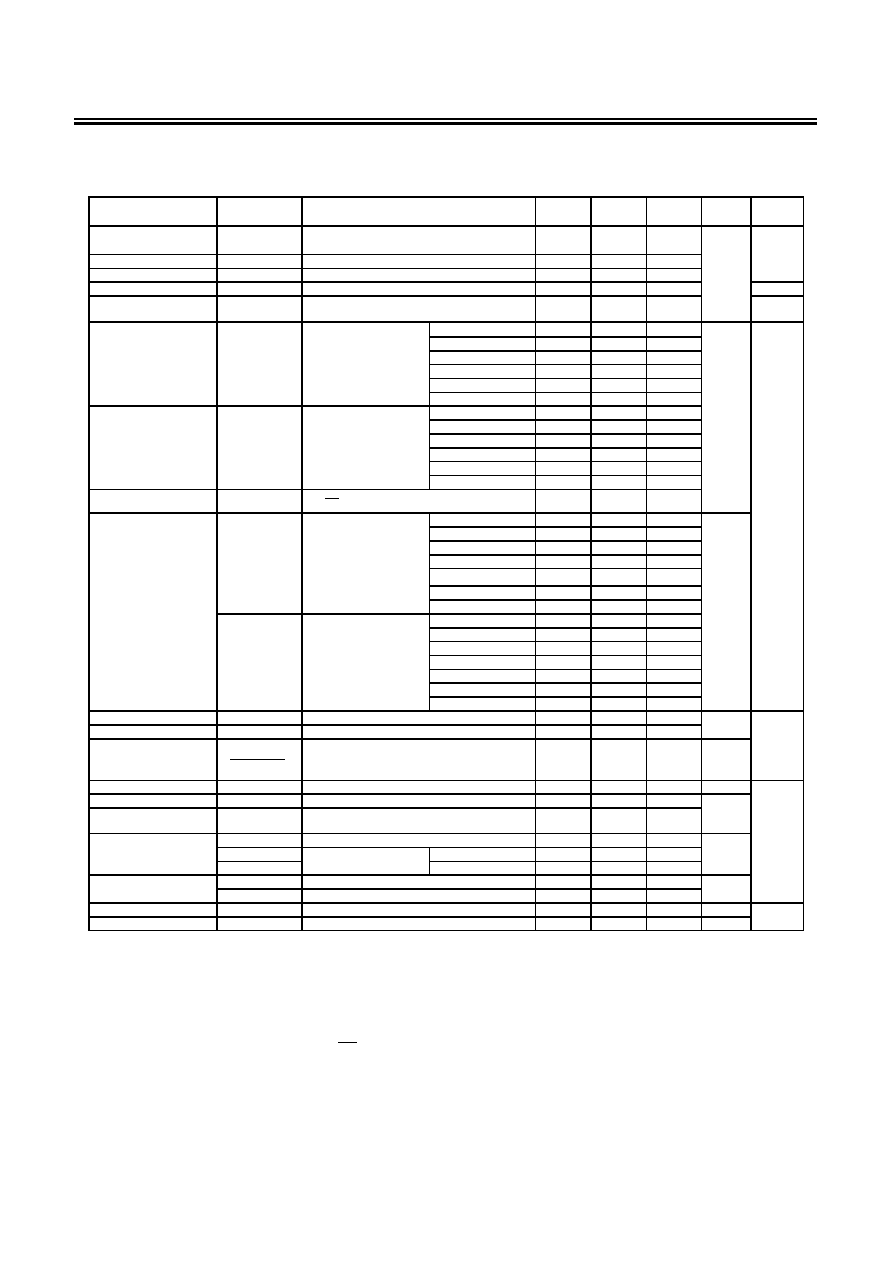
Test Circuits
1.
Figure 9
VSS
VOUT
(VDD)
EXT
(ON/OFF)
Oscilloscope
0.1
ĶF
-
+
A
2.
0.1
ĶF
V
-
+
-
+
(VDD)
VSS
VOUT
(ON/OFF)
EXT
R
b
C
b
Figure 10
3.
Figure 11
0.1
ĶF
VSS
VOUT
(VDD)
EXT
(ON/OFF)
Oscilloscope
-
+
A
4.
Figure 12
0.1
ĶF
V
-
+
-
+
(VDD)
VSS
VOUT
(ON/OFF)
EXT
R
b
C
b

SUPER-SMALL PACKAGE PWM CONTROL, PWM/PFM SWITCHING CONTROL STEP-UP SWITCHING REGULATOR
S-8355/56/57/58 Series
Rev.4.1
_00
18
Seiko Instruments Inc.
Operation
1. Switching control types
1-1. PWM control (S-8355/57 Series)
The S-8355/57 Series is a DC-DC converter using a pulse width modulation method (PWM) and
features a low current consumption.
In conventional PFM DC-DC converters, pulses are skipped when the output load current is low,
causing a fluctuation in the ripple frequency of the output voltage, resulting in an increase in the ripple
voltage.
In S-8355/57 Series, the switching frequency does not change, although the pulse width changes from
0% to 83% (78% for F, G, H, J, L, M, N, P, Q types) corresponding to each load current. The ripple
voltage generated from switching can thus be removed easily through a filter because the switching
frequency is constant.
1-2. PWM/PFM switching control (S-8356/58 Series)
S-8356/58 Series is a DC-DC converter that automatically switches between a pulse width modulation
method (PWM) and a pulse frequency modulation method (PFM), depending on the load current, and
features a low current consumption. This series is a particularly highly efficient DC-DC converter at an
output current of around 100
ĶA.
In conventional constant-duty PFM DC-DC converters, pulses are skipped when the output load
current is low, causing a fluctuation in the ripple frequency of the output voltage, resulting in an increase
in the ripple voltage. The S-8356/58 Series operates under PWM control with the pulse width duty
changing from 15% to 83% (78% for F, G, H, J, L, M, N, P, Q types) in a high output load current area.
On the other hand, the S-8356/58 Series operates under PFM control with the pulse width duty fixed at
15% in a low output load current area, and pulses are skipped when the low output load current is low
according to the load current and output to the switching transistor. The oscillation circuit thus oscillates
intermittently so that the resultant lower self-consumption can prevent a reduction in the efficiency at a
low load current. The switching point from PWM control to PFM control depends on the external
devices (coil, diode, etc.), input voltage and output voltage.
2. Soft start function
For this IC, the built-in soft start circuit controls the rush current and overshoot of the output voltage
when powering on or when the ON/OFF pin is switched to the "H" level.

SUPER-SMALL PACKAGE PWM CONTROL, PWM/PFM SWITCHING CONTROL STEP-UP SWITCHING REGULATOR
Rev.4.1
_00
S-8355/56/57/58 Series
Seiko Instruments Inc.
19
3. Shutdown pin (Only for SOT-23-5 package products of B, H, F, K, L, M, N, and Q types and for 6-Pin
SNB(B) package products.)
Stops or starts step-up operation.
Switching the shutdown pin to the "L" level stops operation of all the internal circuits and reduces the
current consumption significantly.
DO NOT use the shutdown pin in a floating state because it has the structure shown in Figure 13 and is
not pulled up or pulled down internally. DO NOT apply voltage of between 0.3 V and 0.75 V to the
shutdown pin because applying such a voltage increases the current consumption. If the shutdown pin
is not used, connect it to the VOUT (VDD for K, L, M, Q types) pin.
The shutdown pin does not have hysteresis.
Table 24
Shutdown Pin
CR Oscillation Circuit
Output Voltage
"H" Operation Fixed
"L" Stop
V
IN
*1
*1. Voltage obtained by subtracting the voltage drop due to DC resistance of the inductor and
the diode forward voltage from V
IN
.
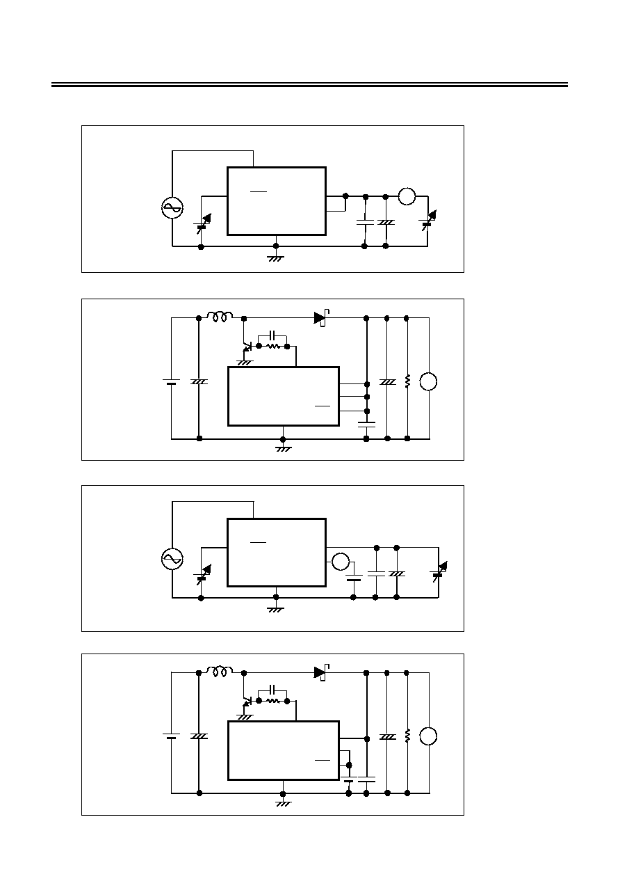
Figure 13 Shutdown Pin Structure
V
VSS
(VDD for K, L , M, Q types)
ON/OFF
VOUT
SUPER-SMALL PACKAGE PWM CONTROL, PWM/PFM SWITCHING CONTROL STEP-UP SWITCHING REGULATOR
S-8355/56/57/58 Series
Rev.4.1
_00
20
Seiko Instruments Inc.
4. Operation
The following are basic equations [(1) through (7)] of the step-up switching regulator (refer to Figure 14).
C
L
M1
D
VOUT
CONT
V
IN
L
+
-
EXT
VSS
Figure 14 Step-up Switching Regulator Circuit for Basic Equations
Voltage at the CONT pin at the moment M1 is turned ON (current I
L
flowing through L is zero), V
A
:
Change in I
L
over time:
Integration of the above equation :
I
L
flows while M1 is ON (t
ON
). The time of t
ON
is determined by the oscillation frequency of OSC.
Peak current (I
PK
) after t
ON
:
The energy stored in L is represented by
∑ ∑ L (I
PK
)
2
.
When M1 is turned OFF (t
OFF
), the energy stored in L is transmitted through a diode to the output capacitor.
Then, reverse voltage (V
L
) is generated:
The voltage at the CONT pin rises only by V
OUT
+ V
D
.
Change in the current (I
L
) flowing through the diode into V
OUT
during t
OFF
:
Integration of the above equation is as follows:
=
=
........................................................... (2)
I
L
=
∑ t
....................................................................... (3)
I
PK
=
∑ t
ON
.................................................................. (4)
=
= ...................................................... (6)
I
L
= I
PK
-
∑ t ..................................................... (7)
....................................................................... (5)
........................................................................................... (1)
*1. V
S
: Non-saturated voltage of M1
V
A
= V
S
*1
dI
L
dt
V
L
L
V
IN
- V
S
L
V
IN
- V
S
L
V
IN
- V
S
L
dI
L
dt
V
L
L
V
OUT
+ V
D
- V
IN
L
L
V
OUT
+ V
D
- V
IN
V
L
= (V
OUT
+ V
D
*2
)
- V
IN
*2. V
D
: Diode forward voltage
1
2

SUPER-SMALL PACKAGE PWM CONTROL, PWM/PFM SWITCHING CONTROL STEP-UP SWITCHING REGULATOR
Rev.4.1
_00
S-8355/56/57/58 Series
Seiko Instruments Inc.
21
During t
ON
, the energy is stored in L and is not transmitted to V
OUT
. When receiving output current (I
OUT
)
from V
OUT
, the energy of the capacitor (C
L
) is consumed. As a result, the pin voltage of C
L
is reduced, and
goes to the lowest level after M1 is turned ON (t
ON
). When M1 is turned OFF, the energy stored in L is
transmitted through the diode to C
L
, and the voltage of C
L
rises drastically. V
OUT
is a time function indicating
the maximum value (ripple voltage: V
P
-P
) when the current flowing through into V
OUT
and load current (I
OUT
)
match.
Next, the ripple voltage is determined as follows:
I
OUT
vs t
1
(time) from when M1 is turned OFF (after t
ON
) to when V
OUT
reaches the maximum level:
When M1 is turned ON (after t
OFF
), I
L
= 0 (when the energy of the inductor is completely transmitted)
:
Based on equation (7),
When substituting equation (10) for equation (9),
Electric charge
Q
1
which is charged in C
L
during t
1
:
When substituting equation (12) for equation (9):
A rise in voltage (V
P
-P
) due to
Q
1
:
When taking into consideration I
OUT
to be consumed during t
1
and ESR
*1
of C
L
:
*1. Equivalent Series Resistance
= ............................................................................................(10)
t
1
= t
OFF
-
∑ t
OFF
................................................................................................... (11)
Q
1
= I
PK
- (I
PK
- I
OUT
)
∑ t
1
= ∑ t
1
.............................................................. (13)
V
P-P
=
=
∑
∑ t
1
+
∑ R
ESR
- ...............
(15)
I
OUT
= I
PK
-
∑ t
1
.................................................................................. (8)
t
1
= (I
PK
- I
OUT
)
∑
.................................................................................. (9)
V
P-P
=
=
∑
∑ t
1
.................................................................... (14)
V
OUT
+ V
D
- V
IN
L
I
PK
t
OFF
I
PK
I
OUT
V
OUT
+ V
D
- V
IN
L
V
OUT
+ V
D
- V
IN
L
Q
1
= I
L
dt
= I
PK
∑ dt - ∑ tdt = I
PK
∑ t
1
- ∑ t
1
2
(12)
V
OUT
+ V
D
- V
IN
L
2
1
t
1
0
V
OUT
+ V
D
- V
IN
L
0
t
1
0
t
1
2
1
2
I
PK
+ I
OUT
C
L
Q
1
C
L
1
2
I
PK
+ I
OUT
C
L
Q
1
C
L
1
2
I
PK
+ I
OUT
C
L
I
OUT
∑ t
1
2
I
PK
+ I
OUT
...........

SUPER-SMALL PACKAGE PWM CONTROL, PWM/PFM SWITCHING CONTROL STEP-UP SWITCHING REGULATOR
S-8355/56/57/58 Series
Rev.4.1
_00
22
Seiko Instruments Inc.
When substituting equation (11) for equation (15):
Therefore to reduce the ripple voltage, it is important that the capacitor connected to the output pin has a
large capacity and a small ESR.
V
P-P
=
∑
+
∑ R
ESR
.................................................. (16)
2I
PK
(I
PK
- I
OUT
)
2
C
L
t
OFF
2
I
PK
+ I
OUT

SUPER-SMALL PACKAGE PWM CONTROL, PWM/PFM SWITCHING CONTROL STEP-UP SWITCHING REGULATOR
Rev.4.1
_00
S-8355/56/57/58 Series
Seiko Instruments Inc.
23
External Parts Selection
The relationship between the major characteristics of the step-up circuit and the characteristics parameters of
the external parts are shown in Figure 15.
For higher efficiency?
For larger output current?
Operation efficiency Stand-by efficiency
For smaller ripple voltage?
Figure 15 Relationship Between Major Characteristics of Step-up Circuit and External Parts
Smaller inductance
Larger inductance
Smaller DC resistance of inductor
Larger output capacitance
With MOS FET, smaller
input capacitance
With MOS FET, smaller ON resistance
With bipolar transistor, smaller external
resistance R
b
With bipolar transistor,
larger external resistance
R
b
Larger output capacitance

SUPER-SMALL PACKAGE PWM CONTROL, PWM/PFM SWITCHING CONTROL STEP-UP SWITCHING REGULATOR
S-8355/56/57/58 Series
Rev.4.1
_00
24
Seiko Instruments Inc.
1. Inductor
The inductance has a strong influence on the maximum output current I
OUT
and efficiency
.
Figure 16 shows the relationship between the I
OUT
and
dependency on L of S-8355/56/57/58.
The peak current (I
PK
) increases by decreasing L and the stability of the circuit improves and I
OUT
increases.
If L is decreased further, the efficiency falls and if the current drive capability is insufficient, I
OUT
decreases.
(Based on the current drive capability of external switching transistor.)
The loss of I
PK
by the switching transistor decreases by increasing L and the efficiency becomes maximum
at a certain L value. Further increasing L decreases the efficiency due to the loss of the DC resistance of
the coil. I
OUT
also decreases.
If the oscillation frequency is higher, a smaller L value can be chosen, making the coil smaller.
The recommended inductances are a 22 to 100
ĶH inductor for B, E, and K types, a 4.7 to 47 ĶH inductor
for F, G, H, J, L, and M types, 3.0 to 22
ĶH inductor for N, P, Q, types.
Choose an inductor so that I
PK
does not exceed the allowable current. Exceeding the allowable current of
the inductor causes magnetic saturation, much lower efficiency and destruction of the IC chip due to a
large current.
I
PK
in discontinuous mode is calculated by the following equation:
f
OSC
= Oscillation frequency, V
D
0.4 V.
2. Diode
Use an external diode that meets the following requirements:
∑ Low forward voltage: (V
F
< 0.3 V)
∑ High switching speed: (50 ns max.)
∑ Reverse voltage: V
OUT
+ V
F
or more
∑ Rated current: I
PK
or more
I
PK
=
2 I
OUT
(V
OUT
+ V
D
- V
IN
)
f
OSC
∑ L
(A) ..............................(17)
CDRH6D28 V
OUT
= 5.0 V, V
IN
= 3.0 V
F, G, H, J, L, M Type
Recommended range
I
OUT
4.7
47
Efficiency
decreases
I
OUT
decreases
I
PK
increases
Coil size:
smaller
Efficiency
decreases
I
OUT
decreases
I
PK
decreases
Coil size:
bigger
L (
ĶH)
Figure 16 L-I
OUT
and
Characteristics
SUPER-SMALL PACKAGE PWM CONTROL, PWM/PFM SWITCHING CONTROL STEP-UP SWITCHING REGULATOR
Rev.4.1
_00
S-8355/56/57/58 Series
Seiko Instruments Inc.
25
3. Capacitor (C
IN
, C
L
)
A capacitor on the input side (C
IN
) improves the efficiency by reducing the power impedance and stabilizing
the input current. Select a C
IN
value according to the impedance of the power supply used.
A capacitor on the output side (C
L
) is used for smoothing the output voltage. For step-up types, the output
voltage flows intermittently to the load current, so step-up types need a larger capacitance than step-down
types. Therefore, select an appropriate capacitor in accordance with the ripple voltage, which increases in
case of a higher output voltage or a higher load current. The capacitor value should be 10
ĶF minimum.
Select an appropriate capacitor taking into consideration the ESR (Equivalent Series Resistance) for
stable output voltage. A stable voltage range in this IC depends on the ESR. Although the inductance (L) is
also a factor, an ESR of 30 m
to 500 m draws out the characteristics. However, the best ESR may
depend on L, the capacitance, the wiring and the application (output load). Therefore, fully evaluate the
ESR under actual conditions to determine the best value.
"2 Ceramic capacitor" of "Application Circuits" shows an example of a circuit that uses a ceramic capacitor
and external resistance (ESR) for reference.
4. External transistor
A bipolar (NPN) transistor or an enhancement (N-channel) MOS FET transistor can be used as the
external transistor.
4.1 Bipolar (NPN) transistor
A circuit example using the CPH3210 (h
FE
= 200 to 560) from Sanyo Electric Co., Ltd. as the bipolar
transistor (NPN) is shown in Figure 19 of "Standard Circuits". The h
FE
value and the R
b
value
determine the driving capacity when the output current is increased using a bipolar transistor. A
peripheral circuit example of the transistor is shown in Figure 17.
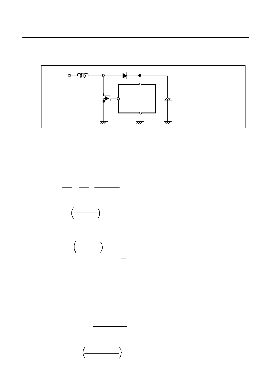
1 k
is recommended for R
b
. R
b
is determined by the following calculation. Calculate the necessary
base current (I
b
) from the bipolar transistor h
FE
using I
b
=
A small R
b
increases the output current, but the efficiency decreases. The current flows pulsating and
there is a voltage drop due to wiring resistance in the actual circuit, therefore the optimum R
b
value
should be determined by experiment.
A speed-up capacitor (C
b
) connected in parallel with the R
b
resistance as shown in Figure 17
decreases the switching loss and improves the efficiency.
C
b
is calculated from the following equation:
However, in practice, the optimum C
b
value also varies depending on the characteristics of the bipolar
transistor employed. Therefore, determine the optimum value by experiment.
VOUT
I
PK
Nch
Pch
R
b
EXT
C
b
2200 pF
1 k
(VDD for E, G, J, K, L, M, P, Q types)
2
∑ R
b
∑ f
OSC
∑ 0.7
1
C
b
for E, G, J, K, L, M, P, and Q types)
(
R
b
=
V
DD
- 0.7
I
b
| I
EXTH
|
0.4
R
b
=
| I
EXTH
|
0.4
I
b
V
OUT
- 0.7
I
PK
h
FE
.
Figure 17 External Transistor Peripheral

SUPER-SMALL PACKAGE PWM CONTROL, PWM/PFM SWITCHING CONTROL STEP-UP SWITCHING REGULATOR
S-8355/56/57/58 Series
Rev.4.1
_00
26
Seiko Instruments Inc.
4.2 Enhancement MOS FET type
Figure 18 is a circuit example using a MOS FET transistor (N-channel).
An N-channel power MOS FET should be used for the MOS FET. Because the gate voltage and
current of the external power MOS FET are supplied from the stepped-up output voltage V
OUT
, the
MOS FET is driven more effectively.
Depending on the MOS FET you use in your device, there is a chance of a current overrun at power
ON. Thoroughly test all settings with your device before deciding on which one to use. Also, try to use
a MOS FET with an input capacitance of 700 pF or less.
Since the ON resistor of the MOS FET might depend on the difference between the output voltage
V
OUT
and the threshold voltage of the MOS FET, and affect the output current as well as the efficiency,
the threshold voltage should be low.
When the output voltage is low, the circuit operates only when the MOS FET has a threshold voltage
lower than the output voltage.
Figure 18 Circuit Example Using MOS FET
VOUT
EXT
VOUT
(ON / OFF)
VSS
(VDD)
-
+
-
+
SUPER-SMALL PACKAGE PWM CONTROL, PWM/PFM SWITCHING CONTROL STEP-UP SWITCHING REGULATOR
Rev.4.1
_00
S-8355/56/57/58 Series
Seiko Instruments Inc.
27
5. V
DD
/V
OUT
separate types (E, G, J, K, L, M, P, and Q types)
The E, G, J, K, L, M, P, and Q types are ideal for the following applications because the power pin for the IC
chip and the VOUT pin for the output voltage are separated:
(1) When changing the output voltage by external resistance.
(2) When outputting a high voltage such as
+15 V or + 20 V.
Choose the products in Table 25 according to applications (1) and (2) above.
Table 25
Output Voltage V
CC
1.8
V
V
CC
< 5 V
5 V
V
CC
Reference
Circuit
S-835xx18
Yes
Yes
Application circuit 1 (Figure 26)
S-835xx50
Yes
Application circuit 1 (Figure 26)
Connection to VDD pin
V
IN
or V
CC
V
IN
Cautions 1. This IC starts a step-up operation at V
DD
=
=
=
= 0.8 V, but set 1.8 V
DD
10 V to stabilize the
output voltage and frequency of the oscillator.
(Input a voltage of 1.8 V or more at the VDD pin for all products with a setting less
than 1.9 V.)
An input voltage of 1.8 V or more at the VDD pin allows connection of the VDD pin to
either the input power pin VIN or output power pin VOUT.
2. Choose external resistors R
A
and R
B
so as to not affect the output voltage,
considering that there is impedance between the VOUT and VSS pins in the IC
chip
.
The internal resistance between the VOUT and VSS pins is as follows:
(1)
S-835xx18
2.1 M
to 14.8 M
(2)
S-835xx20
1.4 M
to 14.8 M
(2)
S-835xx30
1.4 M
to 14.2 M
(3)
S-835xx50
1.4 M
to 12.1 M
3. Attach a capacitor (C
C
) in parallel to the R
A
resistance when an unstable event such
as oscillation of the output voltage occurs. Calculate C
C
using the following
equation:
2
∑
∑
∑
∑ ∑∑∑∑ R
A
∑
∑
∑
∑ 20 kHz
1
C
C
(F)
=
=
=
=
SUPER-SMALL PACKAGE PWM CONTROL, PWM/PFM SWITCHING CONTROL STEP-UP SWITCHING REGULATOR
S-8355/56/57/58 Series
Rev.4.1
_00
28
Seiko Instruments Inc.
(1) S-8357BxxMA, S-8357BxxUA, S-8358BxxMA, S-8358BxxUA
(2) S-8357BxxMC, S-8357FxxMC/BD, S-8357HxxMC/BD, S-8357NxxMC/BD
S-8358BxxMC, S-8358FxxMC/BD, S-8358HxxMC/BD, S-8358NxxMC/BD
Standard Circuits
(3) S-8357ExxMC, S-8357GxxMC/BD, S-8357JxxMC/BD, S-8357PxxMC/BD
S-8358ExxMC, S-8358GxxMC/BD, S-8358JxxMC/BD, S-8358PxxMC/BD
SD
C
L
V
IN
L
1 k
VOUT
VSS
EXT
-
+
-
+
-
+
PWM or PWM
/PFM switching
control circuit
Soft start
built-in reference
power supply
Phase
compensation
circuit
Oscillation circuit
IC internal
power supply
2200 pF
C
IN
Remark The power supply for the IC
chip is from the VOUT pin.
Figure 19
Figure 20
SD
Remark The power supply for
the IC chip is from the
VOUT pin.
-
+
-
+
1 k
V
IN
L
VOUT
VSS
EXT
-
+
2200 pF
C
IN
ON/OFF
C
L
PWM or PWM
/PFM switching
control circuit
Soft start
built-in reference
power supply
Phase
compensation
circuit
Oscillation circuit
IC internal
power supply
Figure 21
Remark The power supply for the IC
chip is from the VDD pin.
-
+
-
+
-
+
C
L
L
SD
1 k
V
IN
VOUT
VSS
EXT
2200 pF
C
IN
VDD
PWM or PWM
/PFM switching
control circuit
Soft start
built-in reference
power supply
Phase
compensation
circuit
Oscillation circuit
IC
internal
power
supply
R
A
R
B
C
C

SUPER-SMALL PACKAGE PWM CONTROL, PWM/PFM SWITCHING CONTROL STEP-UP SWITCHING REGULATOR
Rev.4.1
_00
S-8355/56/57/58 Series
Seiko Instruments Inc.
29
(4) S-8357ExxMC, S-8357GxxMC/BD, S-8357JxxMC/BD
S-8358ExxMC, S-8358GxxMC/BD, S-8358JxxMC/BD
(5) S-8355KxxMC/BD, S-8355LxxMC/BD, S-8355MxxMC/BD, S-8355QxxMC/BD
S-8356KxxMC/BD, S-8356LxxMC/BD, S-8356MxxMC/BD, S-8356QxxMC/BD
(6) S-8355KxxMC/BD, S-8355LxxMC/BD, S-8355MxxMC/BD
S-8356KxxMC/BD, S-8356LxxMC/BD, S-8356MxxMC/BD
Figure 22
Remark The power supply for the IC
chip is from the VDD pin.
SD
1 k
V
IN
VOUT
VSS
EXT
2200 pF
C
IN
VDD
-
+
-
+
C
L
L
-
+
PWM or PWM
/PFM switching
control circuit
Soft start
built-in reference
power supply
Phase
compensation
circuit
Oscillation circuit
IC
internal
power
supply
-
+
-
+
C
L
ON/OFF
L
1 k
V
IN
VOUT
VSS
EXT
2200 pF
C
IN
VDD
-
+
PWM or PWM
/PFM switching
control circuit
Soft start
built-in reference
power supply
Phase
compensation
circuit
Oscillation circuit
IC
internal
power
supply
Remark The power supply for
the IC chip is from the
VDD pin.
Figure 24
Figure 23
-
+
-
+
-
+
C
L
ON/OFF
L
SD
1 k
V
IN
VSS
EXT
2200 pF
C
IN
VDD
PWM or PWM
/PFM switching
control circuit
Soft start
built-in reference
power supply
Phase
compensation
circuit
Oscillation circuit
IC
internal
power
supply
Remark The power supply for the
IC chip is from the VDD
pin.
R
A
C
C
R
B

SUPER-SMALL PACKAGE PWM CONTROL, PWM/PFM SWITCHING CONTROL STEP-UP SWITCHING REGULATOR
S-8355/56/57/58 Series
Rev.4.1
_00
30
Seiko Instruments Inc.
Power Dissipation of Package
Precautions
∑ Mount external capacitors, the diode, and the coil as close as possible to the IC.
∑ Characteristics ripple voltage and spike noise occur in IC containing switching regulators. Moreover rush
current flows at the time of a power supply injection. Because these largely depend on the coil, the
capacitor and impedance of power supply used, fully check them using an actually mounted model.
∑ Make sure that the dissipation of the switching transistor (especially at a high temperature) does not
exceed the allowable power dissipation of the package.
∑ The performance of this IC varies depending on the design of the PCB patterns, peripheral circuits and
external parts. Thoroughly test all settings with your device. Also, try to use the recommended external
parts. If not, contact an SII sales person.
∑ Do not apply an electrostatic discharge to this IC that exceeds the performance ratings of the built-in
electrostatic protection circuit.
∑ SII claims no responsibility for any disputes arising out of or in connection with any infringement by
products including this IC of patents owned by a third party.
Figure 25 Power Dissipation of Package (Before Mounting)
0
50
100
150
600
400
200
0
Power
Dissipation
P
D
(mW)
Ambient Temperature Ta (
įC)
SOT-23-3
SOT-89-3
6-Pin SNB(B)
SOT-23-5
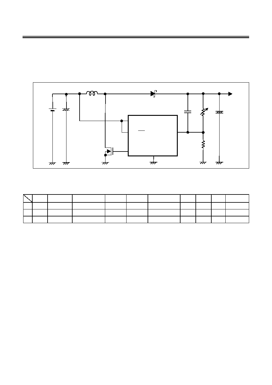
SUPER-SMALL PACKAGE PWM CONTROL, PWM/PFM SWITCHING CONTROL STEP-UP SWITCHING REGULATOR
Rev.4.1
_00
S-8355/56/57/58 Series
Seiko Instruments Inc.
31
Application Circuits
1. LCD Power Supply
The following example is an application power supply circuit (15 V/20 V output) to drive an LCD panel, and its
characteristics.
Figure 26 Power Supply Circuit for LCD
Table 26
Output
Voltage
IC
L Type Name
TR Type
Name
SD Type
Name
C
L
R
a
R
b
C
c
Output
Characteristics
(1) 15
V S-8356M50 CDRH5D18-220
MCH3405 MA2Z748
F93 (20 V,10
ĶF) 580 k 300 k 15 pF (1-a),(1-b)
(2) 20
V S-8356M50
CDRH5D18-220
FDN337N MA729 F93 (25 V,10
ĶF) 575 k 200 k 15 pF (2-a),(2-b)
(3) 10
V S-8356Q50 CDRH5D18-100
MCH3405 MA2Z748
F93 (20 V,10
ĶF) 560 k 560 k 15 pF (3-a),(3-b)
SD
S-8356M50
S-8356Q50
EXT
VOUT
VSS
VDD
ON/OFF
V
OUT
C
L
C
C
L
R
B
R
A
TR
C
IN
V
IN
-
+
+
-

SUPER-SMALL PACKAGE PWM CONTROL, PWM/PFM SWITCHING CONTROL STEP-UP SWITCHING REGULATOR
S-8355/56/57/58 Series
Rev.4.1
_00
32
Seiko Instruments Inc.
(1-a) Output current (I
OUT
) vs. Efficiency (
)
(1-b) Output current (I
OUT
) vs. Output voltage (V
OUT
)
0
20
40
60
80
100
0.01 0.1 1 10 100
[%]
I
OUT
[mA]
V
IN
=3.0 V
V
IN
=5.0 V
V
IN
=7.0 V
12
13
14
15
16
0.01 0.1 1 10 100
V
IN
=3.0 V
V
IN
=5.0 V
V
IN
=7.0 V
V
OU
T
[V]
I
OUT
[mA]
(2-a) Output current (I
OUT
) vs. Efficiency (
)
(2-b) Output current (I
OUT
) vs. Output voltage (V
OUT
)
0
20
40
60
80
100
0.01 0.1 1 10 100
[%]
I
OUT
[mA]
V
IN
=3.0 V
V
IN
=5.0 V
V
IN
=7.0 V
14
16
18
20
22
0.01 0.1 1 10 100
I
OUT
[mA]
V
OU
T
[V]
V
IN
=3.0 V
V
IN
=5.0 V
V
IN
=7.0 V
(3-a) Output current (I
OUT
) vs. Efficiency (
)
(3-b) Output current (I
OUT
) vs. Output voltage (V
OUT
)
0
20
40
60
80
100
0.01 0.1 1 10 100
[%
]
I
OUT
[mA]
V
IN
=3.3 V
V
IN
=5.0 V
8
9
10
0.01 0.1 1 10 100
I
OUT
[mA]
V
OU
T
[V
]
7
V
IN
=3.3 V
V
IN
=5.0 V
11
Figure 27 LCD Power Supply Output Characteristics

SUPER-SMALL PACKAGE PWM CONTROL, PWM/PFM SWITCHING CONTROL STEP-UP SWITCHING REGULATOR
Rev.4.1
_00
S-8355/56/57/58 Series
Seiko Instruments Inc.
33
2. Ceramic Capacitor (Application Example)
If using small ESR parts such as ceramic capacitors for the output capacitance, attach a resistor (R1)
corresponding to the ESR in series to the ceramic capacitor (C
L
) as shown in the following circuit.
R1 may depend on L, the capacitance, the wiring, and the application (output load).
The following example is a circuit using R1
= 100 m, output voltage = 3.3 V, output load = 500 mA and its
characteristics.
Figure 28 Circuit Using Ceramic Capacitor
Table 27
IC
L Type Name
TR Type
Name
SD Type
Name
C
L
(Ceramic Capacitor)
R1 Output
Characteristics
(1) S-8357F33 CDRH6D28-220
FDN335N M1FH3
10
ĶF ◊ 2
100 m
(1-a), (1-b), (1-c)
(2) S-8358B50 CDRH6D28-470 FDN335N M1FH3
10
ĶF ◊ 2
100 m
(2-a), (2-b), (2-c)
(3) S-8357N33 CDRH6D28-100 FDN335N M1FH3
10
ĶF ◊ 2
100 m
(3-a), (3-b), (3-c)
EXT
VOUT
VSS
V
OUT
SD
C
L
L
R1
TR
V
IN
C
IN

SUPER-SMALL PACKAGE PWM CONTROL, PWM/PFM SWITCHING CONTROL STEP-UP SWITCHING REGULATOR
S-8355/56/57/58 Series
Rev.4.1
_00
34
Seiko Instruments Inc.
(1-a) Output current (I
OUT
) vs. Efficiency (
)
(1-b) Output current (I
OUT
) vs. Output voltage (V
OUT
)
0
20
40
60
80
100
0.01 0.1 1 10 100 1000
[%]
I
OUT
[mA]
V
IN
=0.9 V
V
IN
=1.8 V
V
IN
=2.7 V
3.28
3.29
3.30
3.31
3.32
0.01 0.1 1 10 100 1000
V
OU
T
[V
]
I
OUT
[mA]
V
IN
=0.9 V
V
IN
=1.8 V
V
IN
=2.7 V
(1-c) Output current (I
OUT
) vs. Ripple voltage (Vr)
0
20
40
60
80
100
0.01 0.1 1 10 100 1000
V
r
[m
V
]
I
OUT
[mA]
V
IN
=0.9 V
V
IN
=1.8 V
V
IN
=2.7 V
(2-a) Output current (I
OUT
) vs. Efficiency (
)
(2-b) Output current (I
OUT
) vs. Output voltage (V
OUT
)
0
20
40
60
80
100
0.01 0.1 1 10 100 1000
[%
]
I
OUT
[mA]
V
IN
=2.0 V
V
IN
=3.0 V
V
IN
=4.0 V
5.03
5.04
5.05
5.06
5.07
0.01 0.1 1 10 100 1000
V
OU
T
[V]
I
OUT
[mA]
V
IN
=2.0 V
V
IN
=3.0 V
V
IN
=4.0 V
(2-c) Output current (I
OUT
) vs. Ripple voltage (Vr)
0
20
40
60
80
100
0.01 0.1 1 10 100 1000
Vr [mV
]
I
OUT
[mA]
V
IN
=2.0 V
V
IN
=3.0 V
V
IN
=4.0 V

SUPER-SMALL PACKAGE PWM CONTROL, PWM/PFM SWITCHING CONTROL STEP-UP SWITCHING REGULATOR
Rev.4.1
_00
S-8355/56/57/58 Series
Seiko Instruments Inc.
35
(3-a) Output current (I
OUT
) vs. Efficiency (
)
(3-b) Output current (I
OUT
) vs. Output voltage (V
OUT
)
0
20
40
60
80
100
0.01 0.1 1 10 100 1000
[%
]
I
OUT
[mA]
V
IN
=0.9 V
V
IN
=1.8 V
V
IN
=2.7 V
3.28
3.29
3.30
3.31
3.32
0.01 0.1 1 10 100 1000
V
OU
T
[V]
I
OUT
[mA]
V
IN
=0.9 V
V
IN
=1.8 V
V
IN
=2.7 V
(3-c) Output current (I
OUT
) vs. Ripple voltage (Vr)
0
20
40
60
80
100
0.01 0.1 1 10 100 1000
Vr
[
m
V
]
I
OUT
[mA]
V
IN
=0.9 V
V
IN
=1.8 V
V
IN
=2.7 V
Figure 29 Ceramic Capacitor Circuit Output Characteristics

SUPER-SMALL PACKAGE PWM CONTROL, PWM/PFM SWITCHING CONTROL STEP-UP SWITCHING REGULATOR
S-8355/56/57/58 Series
Rev.4.1
_00
36
Seiko Instruments Inc.
Example of Major Temperature Characteristics (Ta
=
=
=
= ----40 to 85įįįįC)
I
SS1
vs. Ta (V
OUT
= 3.3 V, f
osc
= 100 kHz)
0
10
20
30
40
50
-40 -20 0 20 40 60 80 100
Ta [
įC]
I
SS1
[
ĶA]
I
SS1
vs. Ta (V
OUT
= 3.3 V, f
osc
= 300 kHz)
0
10
20
30
40
50
-40 -20 0 20 40 60 80 100
Ta [
įC]
I
SS1
[
ĶA]
I
SS1
vs. Ta (V
OUT
= 3.3 V, f
osc
= 600 kHz)
0
20
40
60
80
100
-40 -20 0 20 40 60 80 100
Ta [
įC]
I
SS1
[
ĶA]
I
SS2
vs. Ta (V
OUT
= 3.3 V, f
osc
= 100 kHz)
0
2
4
6
8
10
-40 -20 0 20 40 60 80 100
Ta [
įC]
I
SS2
[
ĶA]
I
SS2
vs. Ta (V
OUT
= 3.3 V, f
osc
= 300 kHz)
0
2
4
6
8
10
-40 -20 0 20 40 60 80 100
Ta [
įC]
I
SS2
[
ĶA]
I
SS2
vs. Ta (V
OUT
= 3.3 V, f
osc
= 600 kHz)
0
2
4
6
8
10
-40 -20 0 20 40 60 80 100
Ta [
įC]
I
SS2
[
ĶA]

SUPER-SMALL PACKAGE PWM CONTROL, PWM/PFM SWITCHING CONTROL STEP-UP SWITCHING REGULATOR
Rev.4.1
_00
S-8355/56/57/58 Series
Seiko Instruments Inc.
37
I
SSS
vs. Ta (V
OUT
= 3.3 V, f
osc
= 100 kHz)
0.0
0.2
0.4
0.6
0.8
1.0
-40 -20 0 20 40 60 80 100
Ta [
įC]
I
SSS
[
ĶA]
I
SSS
vs. Ta (V
OUT
= 3.3 V, f
osc
= 300 kHz)
0.0
0.2
0.4
0.6
0.8
1.0
-40 -20 0 20 40 60 80 100
Ta [
įC]
I
SSS
[
ĶA]
I
EXTH
vs. Ta (V
OUT
= 3.3 V,f
osc
= 300 kHz)
-
-10
-20
-30
-40
-50
-60
-40 -20 0 20 40 60 80 100
Ta [
įC]
I
EXTH
[mA]
0
I
EXTL
vs. Ta (V
OUT
= 3.3 V,f
osc
= 300 kHz)
0
10
20
30
40
50
60
-40 -20 0 20 40 60 80 100
Ta [
įC]
I
EXTL
[mA]
f
osc
vs. Ta (V
OUT
= 3.3 V, f
osc
= 100 kHz)
50
75
100
125
150
-40 -20 0 20 40 60 80 100
Ta [
įC]
f
osc
[kHz]
f
osc
vs. Ta (V
OUT
= 3.3 V, f
osc
= 300 kHz)
200
250
300
350
400
-40 -20 0 20 40 60 80 100
Ta [
įC]
f
osc
[kHz]
f
osc
vs. Ta (V
OUT
= 3.3 V, f
osc
= 600 kHz)
400
500
600
700
800
-40 -20 0 20 40 60 80 100
Ta [
įC]
f
osc
[kHz]

SUPER-SMALL PACKAGE PWM CONTROL, PWM/PFM SWITCHING CONTROL STEP-UP SWITCHING REGULATOR
S-8355/56/57/58 Series
Rev.4.1
_00
38
Seiko Instruments Inc.
MaxDuty vs. Ta (V
OUT
= 3.3 V, f
osc
= 100 kHz)
70
75
80
85
90
-40 -20 0 20 40 60 80 100
Ta [
įC]
MaxDuty
[%]
MaxDuty vs. Ta (V
OUT
= 3.3 V, f
osc
= 300 kHz)
70
75
80
85
90
-40 -20 0 20 40 60 80 100
Ta [
įC]
MaxDuty
[%]
MaxDuty vs. Ta (V
OUT
= 3.3 V, f
osc
= 600 kHz)
70
75
80
85
90
-40 -20 0 20 40 60 80 100
Ta [
įC]
MaxDuty
[%]
PFMDuty vs. Ta (V
OUT
= 3.3 V, f
osc
= 100 kHz)
S-8356/58 Series
5
10
15
20
25
-40 -20 0 20 40 60 80 100
Ta [
įC]
PFMDuty
[%]
V
SH
vs. Ta (V
OUT
= 3.3 V, f
osc
= 300 kHz)
0.0
0.2
0.4
0.6
0.8
1.0
-40 -20 0 20 40 60 80 100
Ta [
įC]
V
SH
[V]
V
SL1
vs. Ta (V
OUT
= 3.3 V, f
osc
= 300 kHz)
0.0
0.2
0.4
0.6
0.8
1.0
-40 -20 0 20 40 60 80 100
Ta [
įC]
V
SL1
[V]
V
SL2
vs. Ta (V
OUT
= 1.4 V, f
osc
= 300 kHz)
0.0
0.2
0.4
0.6
0.8
1.0
-40 -20 0 20 40 60 80 100
Ta [
įC]
V
SL2
[V]
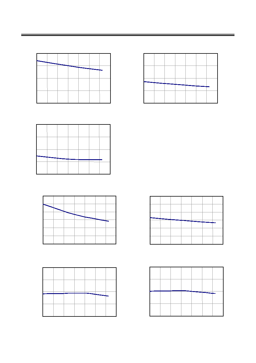
SUPER-SMALL PACKAGE PWM CONTROL, PWM/PFM SWITCHING CONTROL STEP-UP SWITCHING REGULATOR
Rev.4.1
_00
S-8355/56/57/58 Series
Seiko Instruments Inc.
39
t
SS
vs. Ta (V
OUT
= 3.3 V, f
OSC
= 100 kHz)
0
2
4
6
8
-40 -20 0 20 40 60 80 100
Ta [
įC]
t
SS
[ms]
t
SS
vs. Ta (V
OUT
= 3.3 V, f
OSC
= 300 kHz)
0
2
4
6
8
-40 -20 0 20 40 60 80 100
Ta [
įC]
t
SS
[ms]
t
SS
vs. Ta (V
OUT
= 3.3 V, f
OSC
= 600 kHz)
0
2
4
6
8
-40 -20 0 20 40 60 80 100
Ta [
įC]
t
SS
[ms]
V
ST1
vs. T
a
(V
OUT
= 3.3 V, f
OSC
= 100 kHz)
0.0
0.2
0.4
0.6
0.8
1.0
1.2
-40 -20 0 20 40 60 80 100
Ta [
įC]
V
ST1
[V]
V
ST2
vs. T
a
(V
OUT
= 3.3 V, f
OSC
= 100 kHz)
0.0
0.2
0.4
0.6
0.8
1.0
1.2
-40 -20 0 20 40 60 80 100
Ta [
įC]
V
ST2
[V]
V
OUT
vs. T
a
(V
OUT
= 3.3 V, f
OSC
= 100 kHz)
3.20
3.25
3.30
3.35
3.40
-40 -20 0 20 40 60 80 100
Ta [
įC]
V
OUT
[V]
V
OUT
vs. T
a
(V
OUT
= 3.3 V, f
OSC
= 300 kHz)
3.20
3.25
3.30
3.35
3.40
-40 -20 0 20 40 60 80 100
Ta [
įC]
V
OUT
[V]

SUPER-SMALL PACKAGE PWM CONTROL, PWM/PFM SWITCHING CONTROL STEP-UP SWITCHING REGULATOR
S-8355/56/57/58 Series
Rev.4.1
_00
40
Seiko Instruments Inc.
V
OUT
vs. T
a
(V
OUT
= 3.3 V, f
OSC
= 600 kHz)
3.20
3.25
3.30
3.35
3.40
-40 -20 0 20 40 60 80 100
Ta [
įC]
V
OUT
[V]

SUPER-SMALL PACKAGE PWM CONTROL, PWM/PFM SWITCHING CONTROL STEP-UP SWITCHING REGULATOR
Rev.4.1
_00
S-8355/56/57/58 Series
Seiko Instruments Inc.
41
Example of Major Power Supply Dependence Characteristics (Ta
=
=
=
= 25įįįįC)
I
SS1,2
vs. V
DD
(V
OUT
= 3.3 V, f
OSC
= 300 kHz)
0
10
20
30
40
50
0 2 4 6 8 10
V
DD
[V]
I
SS1,2
[
ĶA]
I
SS1,2
vs. V
DD
(V
OUT
= 3.3 V, f
OSC
= 600 kHz)
0
20
40
60
80
100
0 2 4 6 8 10
V
DD
[V]
I
SS1,2
[
ĶA]
I
SSS
vs. V
DD
(V
OUT
= 3.3 V, f
OSC
= 300 kHz)
0.0
0.2
0.4
0.6
0.8
1.0
0 2 4 6 8 10
V
DD
[V]
I
SSS
[
ĶA]
f
OSC
vs. V
DD
(f
OSC
= 100 kHz)
20
40
60
80
100
120
0 2 4 6 8 10
V
DD
[V]
fosc
[kHz]
f
OSC
vs. V
DD
(f
OSC
= 300 kHz)
60
120
180
240
300
360
0 2 4 6 8 10
V
DD
[V]
fosc
[kHz]
f
OSC
vs. V
DD
(f
OSC
= 600 kHz)
120
240
360
480
600
720
0 2 4 6 8 10
V
DD
[V]
fosc
[kHz]

SUPER-SMALL PACKAGE PWM CONTROL, PWM/PFM SWITCHING CONTROL STEP-UP SWITCHING REGULATOR
S-8355/56/57/58 Series
Rev.4.1
_00
42
Seiko Instruments Inc.
MaxDuty vs. V
DD
(f
OSC
= 100 kHz)
50
60
70
80
90
100
0 2 4 6 8 10
V
DD
[V]
MaxDuty
[%]
MaxDuty vs. V
DD
(f
OSC
= 300 kHz)
50
60
70
80
90
100
0 2 4 6 8 10
V
DD
[V]
MaxDuty
[%]
MaxDuty vs. V
DD
(f
OSC
= 600 kHz)
50
60
70
80
90
100
0 2 4 6 8 10
V
DD
[V]
MaxDuty
[%]
I
EXTH
vs. V
DD
-
-20
-40
-60
-80
-100
0 2 4 6 8 10
V
DD
[V]
I
EXTH
[mA]
0
I
EXTL
vs. V
DD
-
-20
-40
-60
-80
-100
0 2 4 6 8 10
V
DD
[V]
I
EXTL
[mA]
0
V
DD
[V]
V
OUT
[V]
1.5
2.0
2.5
3.0
3.5
0 2 4 6 8 10
V
OUT
vs. V
DD
(V
OUT
= 3.3 V, f
OSC
= 100 kHz, V
DD
separate type)
V
IN
= 1.98 V, I
OUT
= 66 mA
V
DD
[V]
V
OUT
[V]
1.5
2.0
2.5
3.0
3.5
0 2 4 6 8 10
V
OUT
vs. V
DD
(V
OUT
= 3.3 V, f
OSC
= 300 kHz, V
DD
separate type)
V
IN
= 1.98 V, I
OUT
= 66 mA

SUPER-SMALL PACKAGE PWM CONTROL, PWM/PFM SWITCHING CONTROL STEP-UP SWITCHING REGULATOR
Rev.4.1
_00
S-8355/56/57/58 Series
Seiko Instruments Inc.
43
V
DD
[V]
V
OUT
[V]
1.5
2.0
2.5
3.0
3.5
0 2 4 6 8 10
V
OUT
vs. V
DD
(V
OUT
= 3.3 V, f
OSC
= 600 kHz, V
DD
separate type)
V
IN
= 1.98 V, I
OUT
= 66 mA

SUPER-SMALL PACKAGE PWM CONTROL, PWM/PFM SWITCHING CONTROL STEP-UP SWITCHING REGULATOR
S-8355/56/57/58 Series
Rev.4.1
_00
44
Seiko Instruments Inc.
Output Waveforms
1. S-8358B33MC
1-1. I
OUT
= 1 mA
1-2. I
OUT
= 20 mA
-25 -20 -15 -10 -5 0 5 10 15 20 25
Time [Ķs]
4
2
0
3.40
3.35
3.30
3.25
Output
voltage
[0.05 V/div]
CONT
voltage
[2.0 V/div]
-25 -20 -15 -10 -5 0 5 10 15 20 25
Time [Ķs]
4
2
0
3.40
3.35
3.30
3.25
Output
voltage
[0.05 V/div]
CONT
voltage
[2.0 V/div]
1-3. I
OUT
= 100 mA
1-4. I
OUT
= 200 mA
-25 -20 -15 -10 -5 0 5 10 15 20 25
Time [
Ķs]
4
2
0
3.40
3.35
3.30
3.25
Output
voltage
[0.05 V/div]
CONT
voltage
[2.0 V/div]
-25 -20 -15 -10 -5 0 5 10 15 20 25
Time [
Ķs]
4
2
0
3.40
3.35
3.30
3.25
Output
voltage
[0.05 V/div]
CONT
voltage
[2.0 V/div]
2. S-8358F33MC
2-1. I
OUT
= 1 mA
2-2. I
OUT
= 10 mA
-10 -8 -6 -4 -2 0 2 4 6 8 10
Time [
Ķs]
4
2
0
3.40
3.35
3.30
3.25
Output
voltage
[0.05 V/div]
CONT
voltage
[2.0 V/div]
-10 -8 -6 -4 -2 0 2 4 6 8 10
4
2
0
3.40
3.35
3.30
3.25
Output
voltage
[0.05 V/div]
CONT
voltage
[2.0 V/div]
Time [
Ķs]
2-3. I
OUT
= 100 mA
2-4. I
OUT
= 200 mA
-10 -8 -6 -4 -2 0 2 4 6 8 10
4
2
0
3.40
3.35
3.30
3.25
Output
voltage
[0.05 V/div]
CONT
voltage
[2.0 V/div]
Time [
Ķs]
-10 -8 -6 -4 -2 0 2 4 6 8 10
4
2
0
3.40
3.35
3.30
3.25
Output
voltage
[0.05 V/div]
CONT
voltage
[2.0 V/div]
Time [
Ķs]
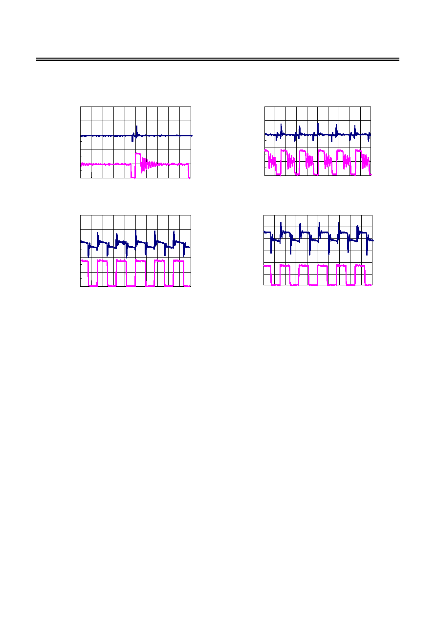
SUPER-SMALL PACKAGE PWM CONTROL, PWM/PFM SWITCHING CONTROL STEP-UP SWITCHING REGULATOR
Rev.4.1
_00
S-8355/56/57/58 Series
Seiko Instruments Inc.
45
3. S-8358N33MC
3-1. I
OUT
= 1 mA
3-2. I
OUT
= 10 mA
-5 -4 -3 -2 -1 0 1 2 3 4 5
4
2
0
3.40
3.35
3.30
3.25
Output
voltage
[0.05 V/div]
CONT
voltage
[2.0 V/div]
Time [
Ķs]
-5 -4 -3 -2 -1 0 1 2 3 4 5
4
2
0
3.40
3.35
3.30
3.25
Output
voltage
[0.05 V/div]
CONT
voltage
[2.0 V/div]
Time [
Ķs]
3-3. I
OUT
= 100 mA
3-4. I
OUT
= 200 mA
-5 -4 -3 -2 -1 0 1 2 3 4 5
4
2
0
3.40
3.35
3.30
3.25
Output
voltage
[0.05 V/div]
CONT
voltage
[2.0 V/div]
Time [
Ķs]
-5 -4 -3 -2 -1 0 1 2 3 4 5
4
2
0
3.40
3.35
3.30
3.25
Output
voltage
[0.05 V/div]
CONT
voltage
[2.0 V/div]
3.20
Time [
Ķs]

SUPER-SMALL PACKAGE PWM CONTROL, PWM/PFM SWITCHING CONTROL STEP-UP SWITCHING REGULATOR
S-8355/56/57/58 Series
Rev.4.1
_00
46
Seiko Instruments Inc.
Examples of Transient Response characteristics
1. Powering ON (V
IN
: 0 V
2.0 V)
1-1. 100 kHz, I
OUT
= 1 mA
1-2. 100 kHz, I
OUT
= 100 mA
0
2
-1 0 1 2 3 4 5 6 7 8 9
time [ms]
V
IN
[V]
0
2
4
V
OUT
[V]
0
2
-1 0 1 2 3 4 5 6 7 8 9
time [ms]
V
IN
[V]
0
2
4
V
OUT
[V]
1-3. 300 kHz, I
OUT
= 1 mA
1-4. 300 kHz, I
OUT
= 100 mA
0
2
-1 0 1 2 3 4 5 6 7 8 9
time [ms]
V
IN
[V]
0
2
4
V
OUT
[V]
0
2
-1 0 1 2 3 4 5 6 7 8 9
time [ms]
V
IN
[V]
0
2
4
V
OUT
[V]
1-5. 600 kHz, I
OUT
= 1 mA
1-6. 600 kHz, I
OUT
= 100 mA
0
2
-1 0 1 2 3 4 5 6 7 8 9
time [ms]
V
IN
[V]
0
2
4
V
OUT
[V]
0
2
-1 0 1 2 3 4 5 6 7 8 9
time [ms]
V
IN
[V]
0
2
4
V
OUT
[V]
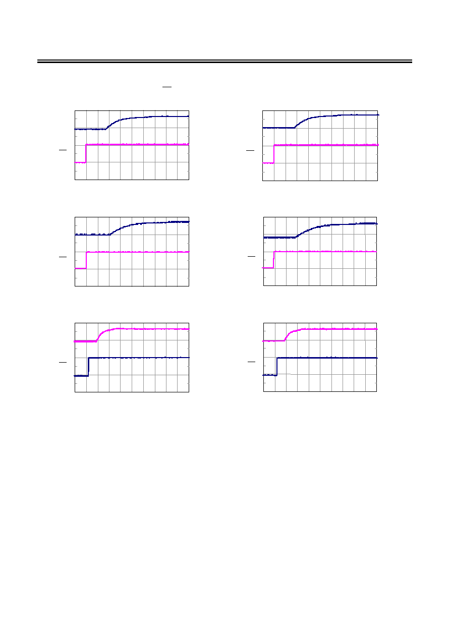
SUPER-SMALL PACKAGE PWM CONTROL, PWM/PFM SWITCHING CONTROL STEP-UP SWITCHING REGULATOR
Rev.4.1
_00
S-8355/56/57/58 Series
Seiko Instruments Inc.
47
2. Responses of shutdown pin (V
ON/OFF
: 0 V
2.0 V)
2-1. 100 kHz, I
OUT
= 1 mA
2-2. 100 kHz, I
OUT
= 100 mA
0
2
-1 0 1 2 3 4 5 6 7 8 9
time [ms]
V
ON/OFF
[V]
0
2
4
V
OUT
[V]
0
2
-1 0 1 2 3 4 5 6 7 8 9
time [ms]
V
ON/OFF
[V]
0
2
4
V
OUT
[V]
2-3. 300 kHz, I
OUT
= 1 mA
2-4. 300 kHz, I
OUT
= 100 mA
0
2
-1 0 1 2 3 4 5 6 7 8 9
time [ms]
V
ON/OFF
[V]
0
2
4
V
OUT
[V]
0
2
-1 0 1 2 3 4 5 6 7 8 9
time [ms]
V
ON/OFF
[V]
0
2
4
V
OUT
[V]
2-5. 600 kHz, I
OUT
= 1 mA
2-6. 600 kHz, I
OUT
= 100 mA
0
2
-1 0 1 2 3 4 5 6 7 8 9
time [ms]
V
ON/OFF
[V]
0
2
4
V
OUT
[V]
0
2
-1 0 1 2 3 4 5 6 7 8 9
time [ms]
V
ON/OFF
[V]
0
2
4
V
OUT
[V]

SUPER-SMALL PACKAGE PWM CONTROL, PWM/PFM SWITCHING CONTROL STEP-UP SWITCHING REGULATOR
S-8355/56/57/58 Series
Rev.4.1
_00
48
Seiko Instruments Inc.
3. Load fluctuations
3-1. 100 kHz, I
OUT
: 100
ĶA 100 mA
3-2. 100 kHz, I
OUT
: 100 mA
100 ĶA
-0.2 0.0 0.2 0.4 0.6 0.8 1.0 1.2 1.4 1.6 1.8
time [ms]
3.00
3.20
3.40
3.60
V
OUT
[0.2 V/div]
100
ĶA
I
OUT
100 mA
-10 0 10 20 30 40 50 60 70 80 90
time [ms]
3.20
3.40
3.60
3.80
V
OUT
[0.2 V/div]
100
ĶA
I
OUT
100 mA
3-3. 300 kHz, I
OUT
: 100
ĶA 100 mA
3-4. 300 kHz, I
OUT
: 100 mA
100 ĶA
-0.5 0.0 0.5 1.0 1.5 2.0 2.5 3.0 3.5 4.0 4.5
time [ms]
3.00
3.20
3.40
3.60
V
OUT
[0.2 V/div]
100
ĶA
I
OUT
100 mA
-10 0 10 20 30 40 50 60 70 80 90
time [ms]
3.20
3.40
3.60
3.80
V
OUT
[0.2 V/div]
100
ĶA
I
OUT
100 mA
3-5. 600 kHz, I
OUT
: 0.1 mA
100 mA
3-6. 600 kHz, I
OUT
: 100 mA
0.1 mA
time [ms]
3.00
3.20
3.40
3.60
V
OUT
[0.2 V/div]
100
ĶA
I
OUT
100 mA
0.0 0.2 0.4 0.6 0.8 1.0 1.2 1.4 1.6 1.8
-0.2
-0.5 0 0.5 1.0 1.5 2.0 2.5 3.0
time [ms]
3.00
3.20
3.40
3.60
V
OUT
[0.2 V/div]
100
ĶA
I
OUT
100 mA
3.80

SUPER-SMALL PACKAGE PWM CONTROL, PWM/PFM SWITCHING CONTROL STEP-UP SWITCHING REGULATOR
Rev.4.1
_00
S-8355/56/57/58 Series
Seiko Instruments Inc.
49
4. Input voltage fluctuations
4-1. 100 kHz, I
OUT
= 100 mA, V
IN
= 1.98 V 2.64 V
4-2. 100 kHz, I
OUT
= 100 mA, V
IN
= 2.64 V 1.98 V
1.5
2.0
2.5
3.0
-0.2 0.0 0.2 0.4 0.6 0.8 1.0 1.2 1.4 1.6 1.8
time [ms]
3.25
3.30
3.35
3.40
3.45
V
IN
[V]
V
OUT
[V]
1.5
2.0
2.5
3.0
-0.2 0.0 0.2 0.4 0.6 0.8 1.0 1.2 1.4 1.6 1.8
time [ms]
3.25
3.30
3.35
3.40
3.45
V
IN
[V]
V
OUT
[V]
4-3. 300 kHz, I
OUT
= 100 mA, V
IN
= 1.98 V 2.64 V
4-4. 100 kHz, I
OUT
= 100 mA, V
IN
=2.64 V 1.98 V
1.5
2.0
2.5
3.0
-0.2 0.0 0.2 0.4 0.6 0.8 1.0 1.2 1.4 1.6 1.8
time [ms]
3.25
3.30
3.35
3.40
3.45
V
IN
[V]
V
OUT
[V]
1.5
2.0
2.5
3.0
-0.2 0.0 0.2 0.4 0.6 0.8 1.0 1.2 1.4 1.6 1.8
time [ms]
3.25
3.30
3.35
3.40
3.45
V
IN
[V]
V
OUT
[V]
4-5. 600 kHz, I
OUT
= 100 mA, V
IN
= 1.98 V 2.64 V
4-6. 600 kHz, I
OUT
= 100 mA, V
IN
= 2.64 V 1.98 V
1.5
2.0
2.5
3.0
-0.2 0.0 0.2 0.4 0.6 0.8 1.0 1.2 1.4 1.6 1.8
time [ms]
3.25
3.30
3.35
3.40
3.45
V
IN
[V]
V
OUT
[V]
1.5
2.0
2.5
3.0
-0.2 0.0 0.2 0.4 0.6 0.8 1.0 1.2 1.4 1.6 1.8
time [ms]
3.25
3.30
3.35
3.40
3.45
V
IN
[V]
V
OUT
[V]

SUPER-SMALL PACKAGE PWM CONTROL, PWM/PFM SWITCHING CONTROL STEP-UP SWITCHING REGULATOR
S-8355/56/57/58 Series
Rev.4.1
_00
50
Seiko Instruments Inc.
Reference Data
Use this reference data to choose the external parts. This reference data makes it possible to choose the
recommended external part based on the application and characteristics data.
1. Reference data for external parts
Table 28 Efficiency vs. Output Characteristics and Output Voltage vs.
Output Current Characteristics for External Parts
No.
Product
Name
Oscillation
Frequency
Output
Voltage
Control
System
Inductor Transistor
Diode
Output
Capacitor
1
S-8357F33
300 kHz
3.3 V
PWM
CDRH104R-220
S-90N0312SMA
M1FH3
F93 (16 V, 47
ĶF) ◊ 2
2
S-8357F50
300 kHz
5.0 V
PWM
3
S-8356M50
300 kHz
5.0 V
PWM/PFM
4
S-8357B33
100 kHz
3.3 V
PWM
CDRH104R-470
5
S-8358B33
100 kHz
3.3 V
PWM/PFM
S-90N0442SUA
6
S-8357B50
100 kHz
5.0 V
PWM
7
S-8356M50
300 kHz
5.0 V
PWM/PFM
CDRH8D28-220
S-90N0212SMA
F93 (16 V, 47
ĶF)
8
S-8357B33
100 kHz
3.3 V
PWM
CDRH8D28-470
9
S-8358B33
100 kHz
3.3 V
PWM/PFM
10
S-8357B50
100 kHz
5.0 V
PWM
11
S-8357F33
300 kHz
3.3 V
PWM
CXLP120-220
MA2Z748
F92 (6.3 V, 47
ĶF)
12
S-8356M50
300 kHz
5.0 V
PWM/PFM
13
S-8357N33
600 kHz
3.3 V
PWM
CDRH8D28-100
M1FH3
F93 (16 V, 47
ĶF)
14
S-8357N50
600 kHz
5.0 V
PWM
15
S-8356Q33
600 kHz
3.3 V
PWM/PFM
16
S-8356Q50
600 kHz
5.0 V
PWM/PFM
The properties of the external parts are shown below.
Table 29 Properties of External Parts
Part Product
Name
Manufacturer
Characteristics
Inductor CDRH104R-220
Sumida
Corporation
22
ĶH, DCR
*1
= 73 m, I
MAX
*2
= 2.5 A, Height = 4.0 mm
CDRH104R-470
47
ĶH, DCR
*1
= 128 m, I
MAX
*2
= 1.9 A, Height = 4.0 mm
CDRH8D28-100
10
ĶH, DCR
*1
= 47 m, I
MAX
*2
= 2.7 A, Height = 3.0 mm
CDRH8D28-220
22
ĶH, DCR
*1
= 99 m, I
MAX
*2
= 1.8 A, Height = 3.0 mm
CDRH8D28-470
47
ĶH, DCR
*1
= 195 m, I
MAX
*2
= 1.25 A, Height = 3.0 mm
CXLP120-220
Sumitomo Special
Metals Co., Ltd.
22
ĶH, DCR
*1
= 590 m, I
MAX
*2
= 0.55 A, Height = 1.2 mm
Diode M1FH3
Shindengen Electric
Manufacturing Co., Ltd.
V
F
*3
= 0.3 V, I
F
*4
= 1.5 A
MA2Z748
Matsushita Electric
Industrial Co., Ltd.
V
F
*3
= 0.4 V, I
F
*4
= 0.3 A
F93
Nichicon Corporation
16 V, 47
ĶF
Capacitor
(Output capacitance)
F92
6.3 V, 47
ĶF
Transistor
(Nch FET)
S-90N0212SMA
Seiko Instruments Inc.
V
DSS
*5
= 20 V max., V
GSS
*6
= 12 V max., C
ISS
*7
= 190 pF,
R
DS(ON)
*8
= 0.16 max. (V
GS
*9
= 2.5 V, I
D
*10
= 0.5 A)
S-90N0312SMA
V
DSS
*5
= 20 V max., V
GSS
*6
= 8 V max., C
ISS
*7
= 170 pF,
R
DS(ON)
*8
= 0.14 max. (V
GS
*9
= 2.5 V, I
D
*10
= 0.5 A)
S-90N0442SUA
V
DSS
*5
= 20 V max., V
GSS
*6
= 8 V max., C
ISS
*7
= 390 pF,
R
DS(ON)
*8
= 0.07 max. (V
GS
*9
= 2.5 V, I
D
*10
= 2.0 A)
*1. DC resistance, *2. Maximum allowable current, *3. Forward voltage, *4. Forward current, *5. Drain-source voltage,
*6. Gate-source voltage, *7. Input capacitance, *8. Drain-source on resistance, *9 Gate-source voltage, *10 Drain current
Caution The values shown in the characteristics column of Table 29 above are based on the materials
provided by each manufacturer. However, consider the characteristics of the original materials when
using the above products.

SUPER-SMALL PACKAGE PWM CONTROL, PWM/PFM SWITCHING CONTROL STEP-UP SWITCHING REGULATOR
Rev.4.1
_00
S-8355/56/57/58 Series
Seiko Instruments Inc.
51
2. Reference data (1)
The data of (a) output current (I
OUT
) vs. efficiency (
) characteristics and (b) output current (I
OUT
) vs. output
voltage (V
OUT
) characteristics under conditions of (1) to (16) shown in Table 28 is shown below.
(1) S-8357F33
(a) Output current (I
OUT
) vs. Efficiency (
)
(b) Output current (I
OUT
) vs. Output voltage (V
OUT
)
20
40
60
80
100
1 10 100
1000
0.1
[
%
]
I
OUT
[mA]
V
IN
=0.9 V
V
IN
=1.8 V
V
IN
=2.7 V
3.0
3.1
3.2
3.3
3.4
3.5
0.1 1 10 100
1000
V
OU
T
[V
]
I
OUT
[mA]
V
IN
=0.9 V
V
IN
=1.8 V
V
IN
=2.7 V
(2) S-8357F50
(a) Output current (I
OUT
) vs. Efficiency (
)
(b) Output current (I
OUT
) vs. Output voltage (V
OUT
)
20
40
60
80
100
1 10 100
1000
0.1
[%
]
I
OUT
[mA]
V
IN
=2.0 V
V
IN
=3.0 V
V
IN
=4.0 V
4.7
4.8
4.9
5.0
5.1
5.2
0.1 1 10 100
1000
V
OU
T
[
V
]
I
OUT
[mA]
V
IN
=2.0 V
V
IN
=3.0 V
V
IN
=4.0 V
(3) S-8356M50
(a) Output current (I
OUT
) vs. Efficiency (
)
(b) Output current (I
OUT
) vs. Output voltage (V
OUT
)
20
40
60
80
100
1 10 100
1000
0.1
[
%
]
I
OUT
[mA]
V
IN
=2.0 V
V
IN
=3.0 V
V
IN
=4.0 V
4.7
4.8
4.9
5.0
5.1
5.2
0.1 1 10 100
1000
V
OU
T
[V
]
I
OUT
[mA]
V
IN
=2.0 V
V
IN
=3.0 V
V
IN
=4.0 V

SUPER-SMALL PACKAGE PWM CONTROL, PWM/PFM SWITCHING CONTROL STEP-UP SWITCHING REGULATOR
S-8355/56/57/58 Series
Rev.4.1
_00
52
Seiko Instruments Inc.
(4) S-8357B33
(a) Output current (I
OUT
) vs. Efficiency (
)
(b) Output current (I
OUT
) vs. Output voltage (V
OUT
)
20
40
60
80
100
1 10 100
1000
0.1
[%
]
I
OUT
[mA]
V
IN
=0.9 V
V
IN
=1.8 V
V
IN
=2.7 V
3.0
3.1
3.2
3.3
3.4
3.5
0.1 1 10 100
1000
V
OU
T
[
V
]
I
OUT
[mA]
V
IN
=0.9 V
V
IN
=1.8 V
V
IN
=2.7 V
(5) S-8358B33
(a) Output current (I
OUT
) vs. Efficiency (
)
(b) Output current (I
OUT
) vs. Output voltage (V
OUT
)
20
40
60
80
100
1 10 100
1000
0.1
[%
]
I
OUT
[mA]
V
IN
=0.9 V
V
IN
=1.8 V
V
IN
=2.7 V
3.0
3.1
3.2
3.3
3.4
3.5
0.1 1 10 100
1000
V
OU
T
[
V
]
I
OUT
[mA]
V
IN
=0.9 V
V
IN
=1.8 V
V
IN
=2.7 V
(6) S-8357B50
(a) Output current (I
OUT
) vs. Efficiency (
)
(b) Output current (I
OUT
) vs. Output voltage (V
OUT
)
20
40
60
80
100
1 10 100
1000
0.1
[
%
]
I
OUT
[mA]
V
IN
=2.0 V
V
IN
=3.0 V
V
IN
=4.0 V
4.7
4.8
4.9
5.0
5.1
5.2
0.1 1 10 100
1000
V
OU
T
[V
]
I
OUT
[mA]
V
IN
=2.0 V
V
IN
=3.0 V
V
IN
=4.0 V
(7) S-8356M50
(a) Output current (I
OUT
) vs. Efficiency (
)
(b) Output current (I
OUT
) vs. Output voltage (V
OUT
)
20
40
60
80
100
1 10
100
1000
0.1
[
%
]
I
OUT
[mA]
V
IN
=2.0 V
V
IN
=3.0 V
V
IN
=4.0 V
4.7
4.8
4.9
5.0
5.1
5.2
0.1 1 10 100
1000
V
OU
T
[
V
]
I
OUT
[mA]
V
IN
=3.0 V
V
IN
=4.0 V
V
IN
=2.0 V

SUPER-SMALL PACKAGE PWM CONTROL, PWM/PFM SWITCHING CONTROL STEP-UP SWITCHING REGULATOR
Rev.4.1
_00
S-8355/56/57/58 Series
Seiko Instruments Inc.
53
(8) S-8357B33
(a) Output current (I
OUT
) vs. Efficiency (
)
(b) Output current (I
OUT
) vs. Output voltage (V
OUT
)
20
40
60
80
100
1 10 100
1000
0.1
[%
]
I
OUT
[mA]
V
IN
=0.9 V
V
IN
=1.8 V
V
IN
=2.7 V
3.0
3.1
3.2
3.3
3.4
3.5
0.1 1 10 100
1000
V
OU
T
[
V
]
I
OUT
[mA]
V
IN
=0.9 V
V
IN
=1.8 V
V
IN
=2.7 V
(9) S-8358B33
(a) Output current (I
OUT
) vs. Efficiency (
)
(b) Output current (I
OUT
) vs. Output voltage (V
OUT
)
20
40
60
80
100
1 10 100
1000
0.1
[
%
]
I
OUT
[mA]
V
IN
=0.9 V
V
IN
=1.8 V
V
IN
=2.7 V
3.0
3.1
3.2
3.3
3.4
3.5
0.1 1 10 100
1000
V
OU
T
[
V
]
I
OUT
[mA]
V
IN
=0.9 V
V
IN
=1.8 V
V
IN
=2.7 V
(10) S-8357B50
(a) Output current (I
OUT
) vs. Efficiency (
)
(b) Output current (I
OUT
) vs. Output voltage (V
OUT
)
20
40
60
80
100
1 10 100
1000
0.1
[%
]
I
OUT
[mA]
V
IN
=2.0 V
V
IN
=3.0 V
V
IN
=4.0 V
4.7
4.8
4.9
5.0
5.1
5.2
0.1 1 10 100
1000
V
OU
T
[V
]
I
OUT
[mA]
V
IN
=2.0 V
V
IN
=3.0 V
V
IN
=4.0 V
(11) S-8357F33
(a) Output current (I
OUT
) vs. Efficiency (
)
(b) Output current (I
OUT
) vs. Output voltage (V
OUT
)
20
40
60
80
100
1 10 100
1000
0.1
[%
]
I
OUT
[mA]
V
IN
=0.9 V
V
IN
=1.8 V
V
IN
=2.7 V
3.0
3.1
3.2
3.3
3.4
3.5
0.1 1 10 100
1000
V
OU
T
[
V
]
I
OUT
[mA]
V
IN
=0.9 V
V
IN
=1.8 V
V
IN
=2.7 V
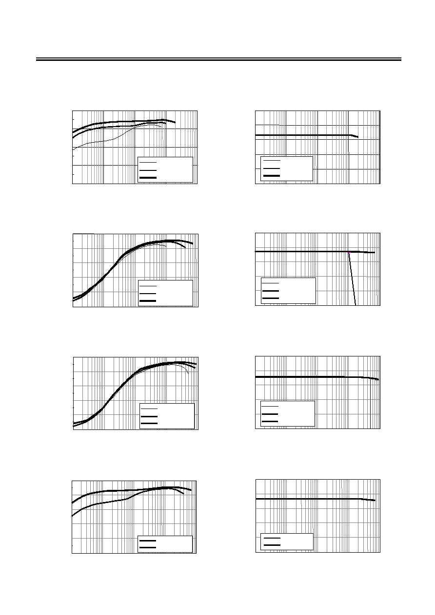
SUPER-SMALL PACKAGE PWM CONTROL, PWM/PFM SWITCHING CONTROL STEP-UP SWITCHING REGULATOR
S-8355/56/57/58 Series
Rev.4.1
_00
54
Seiko Instruments Inc.
(12) S-8356M50
(a) Output current (I
OUT
) vs. Efficiency (
)
(b) Output current (I
OUT
) vs. Output voltage (V
OUT
)
20
40
60
80
100
1 10 100
1000
0.1
[
%
]
I
OUT
[mA]
V
IN
=2.0 V
V
IN
=3.0 V
V
IN
=4.0 V
4.7
4.8
4.9
5.0
5.1
5.2
0.1 1 10 100
1000
V
OU
T
[
V
]
I
OUT
[mA]
V
IN
=2.0 V
V
IN
=3.0 V
V
IN
=4.0 V
(13) S-8357N33
(a) Output current (I
OUT
) vs. Efficiency (
)
(b) Output current (I
OUT
) vs. Output voltage (V
OUT
)
20
40
60
80
100
1 10 100
1000
0.1
[
%
]
I
OUT
[mA]
0
V
IN
=0.9 V
V
IN
=1.8 V
V
IN
=2.7 V
3.0
3.1
3.2
3.3
3.4
3.5
V
OU
T
[
V
]
1 10
100
1000
0.1
I
OUT
[mA]
V
IN
=0.9 V
V
IN
=1.8 V
V
IN
=2.7 V
(14) S-8357N50
(a) Output current (I
OUT
) vs. Efficiency (
)
(b) Output current (I
OUT
) vs. Output voltage (V
OUT
)
20
40
60
80
100
1 10
100
1000
0.1
[
%
]
I
OUT
[mA]
0
V
IN
=2.0 V
V
IN
=3.0 V
V
IN
=4.0 V
4.7
4.8
4.9
5.0
5.1
5.2
V
OU
T
[
V
]
1 10
100
1000
0.1
I
OUT
[mA]
V
IN
=2.0 V
V
IN
=3.0 V
V
IN
=4.0 V
(15) S-8356Q33
(a) Output current (I
OUT
) vs. Efficiency (
)
(b) Output current (I
OUT
) vs. Output voltage (V
OUT
)
20
40
60
80
100
1 10 100
1000
0.1
[
%
]
I
OUT
[mA]
0
V
IN
=1.8 V
V
IN
=2.7 V
3.0
3.1
3.2
3.3
3.4
3.5
V
OU
T
[V
]
1 10
100
1000
0.1
I
OUT
[mA]
V
IN
=1.8 V
V
IN
=2.7 V

SUPER-SMALL PACKAGE PWM CONTROL, PWM/PFM SWITCHING CONTROL STEP-UP SWITCHING REGULATOR
Rev.4.1
_00
S-8355/56/57/58 Series
Seiko Instruments Inc.
55
(16) S-8356Q50
(a) Output current (I
OUT
) vs. Efficiency (
)
(b) Output current (I
OUT
) vs. Output voltage (V
OUT
)
20
40
60
80
100
1 10 100
1000
0.1
[
%
]
I
OUT
[mA]
0
V
IN
=3.0 V
V
IN
=4.0 V
4.7
4.8
4.9
5.0
5.1
5.2
V
OU
T
[V
]
1 10
100
1000
0.1
I
OUT
[mA]
V
IN
=3.0 V
V
IN
=4.0 V

SUPER-SMALL PACKAGE PWM CONTROL, PWM/PFM SWITCHING CONTROL STEP-UP SWITCHING REGULATOR
S-8355/56/57/58 Series
Rev.4.1
_00
56
Seiko Instruments Inc.
3. Reference data (2)
The actual output current vs. ripple voltage characteristics data under conditions of (1) to (16) in Table 28
are shown below.
(1) S-8357F33
(2) S-8357F50
0
50
100
150
Vr
[
m
V]
I
OUT
[mA]
0.1 1 10 100
1000
V
IN
=0.9 V
V
IN
=1.8 V
V
IN
=2.7 V
0
50
100
150
Vr
[
m
V]
I
OUT
[mA]
0.1 1 10 100
1000
V
IN
=2.0 V
V
IN
=3.0 V
V
IN
=4.0 V
(3) S-8356M50
(4) S-8357B33
0
50
100
150
V
r
[m
V
]
I
OUT
[mA]
0.1 1 10 100
1000
V
IN
=2.0 V
V
IN
=3.0 V
V
IN
=4.0 V
0
50
100
150
Vr
[
m
V]
I
OUT
[mA]
0.1 1 10 100
1000
V
IN
=0.9 V
V
IN
=1.8 V
V
IN
=2.7 V
(5) S-8358B33
(6) S-8357B50
0
50
100
150
V
r
[m
V
]
I
OUT
[mA]
0.1 1 10 100
1000
V
IN
=0.9 V
V
IN
=1.8 V
V
IN
=2.7 V
0
50
100
150
Vr
[
m
V]
I
OUT
[mA]
0.1 1 10 100
1000
V
IN
=2.0 V
V
IN
=3.0 V
V
IN
=4.0 V
(7) S-8356M50
(8) S-8357B33
0
50
100
150
Vr
[
m
V]
I
OUT
[mA]
0.1 1 10 100
1000
V
IN
=2.0 V
V
IN
=3.0 V
V
IN
=4.0 V
0
50
100
150
Vr
[
m
V]
I
OUT
[mA]
0.1 1 10 100
1000
V
IN
=0.9 V
V
IN
=1.8 V
V
IN
=2.7 V

SUPER-SMALL PACKAGE PWM CONTROL, PWM/PFM SWITCHING CONTROL STEP-UP SWITCHING REGULATOR
Rev.4.1
_00
S-8355/56/57/58 Series
Seiko Instruments Inc.
57
(9) S-8358B33
(10) S-8357B50
0
50
100
150
Vr
[
m
V]
I
OUT
[mA]
0.1 1 10 100
1000
V
IN
=0.9 V
V
IN
=1.8 V
V
IN
=2.7 V
0
50
100
150
Vr
[
m
V]
I
OUT
[mA]
0.1 1 10 100
1000
V
IN
=2.0 V
V
IN
=3.0 V
V
IN
=4.0 V
(11) S-8357F33
(12) S-8356M50
0
50
100
150
Vr
[
m
V]
I
OUT
[mA]
0.1 1 10 100
1000
V
IN
=0.9 V
V
IN
=1.8 V
V
IN
=2.7 V
0
50
100
150
Vr
[
m
V]
I
OUT
[mA]
0.1 1 10 100
1000
V
IN
=2.0 V
V
IN
=3.0 V
V
IN
=4.0 V
(13) S-8357N33
(14) S-8357N50
V
r
[m
V
]
I
OUT
[mA]
0.1 1 10 100
1000
20
40
60
80
100
0
V
IN
=0.9 V
V
IN
=1.8 V
V
IN
=2.7 V
Vr
[
m
V]
I
OUT
[mA]
0.1 1 10 100
1000
20
40
60
80
100
0
V
IN
=2.0 V
V
IN
=3.0 V
V
IN
=4.0 V
(15) S-8356Q33
(16) S-8356Q50
Vr
[
m
V]
I
OUT
[mA]
0.1 1 10 100
1000
20
40
60
80
100
0
V
IN
=1.8 V
V
IN
=2.7 V
Vr
[
m
V]
I
OUT
[mA]
0.1 1 10 100
1000
20
40
60
80
100
0
V
IN
=3.0 V
V
IN
=4.0 V

No.
TITLE
SCALE
UNIT
mm
Seiko Instruments Inc.
0.4Ī0.05
1.5Ī0.1
4.5Ī0.1
1.6Ī0.2
1.5Ī0.1 1.5Ī0.1
0.45Ī0.1
0.4Ī0.1
0.4Ī0.1
45į
3
1
2
No. UP003-A-P-SD-1.1
UP003-A-P-SD-1.1
SOT893-A-PKG Dimensions

No.
TITLE
SCALE
UNIT
mm
Seiko Instruments Inc.
2.0Ī0.1
0.3Ī0.05
8.0Ī0.1
Ý1.5
+0.1
-0
2.0Ī0.05
Ý1.5
+0.1
-0
4.75Ī0.1
5į max.
No. UP003-A-C-SD-1.1
UP003-A-C-SD-1.1
SOT893-A-Carrier Tape
Feed direction
4.0Ī0.1(10 pitches : 40.0Ī0.2)

No.
TITLE
SCALE
UNIT
mm
Seiko Instruments Inc.
13.0Ī0.3
16.5max.
(60į)
(60į)
QTY.
1,000
No. UP003-A-R-SD-1.1
UP003-A-R-SD-1.1
SOT893-A-Reel
Enlarged drawing in the central part
No.
TITLE
SCALE
UNIT
mm
Seiko Instruments Inc.
2.9Ī0.2
0.95Ī0.1
1.9Ī0.2
+0.1
-0.05
0.16
0.4Ī0.1
1
2
3
No. MP003-A-P-SD-1.1
MP003-A-P-SD-1.1
SOT233-A-PKG Dimensions
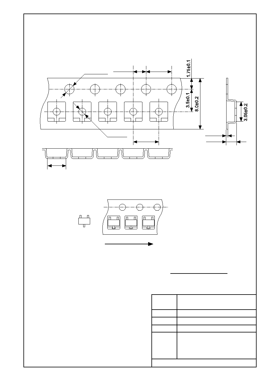
No.
TITLE
SCALE
UNIT
mm
Seiko Instruments Inc.
1.6Ī0.1
0.25Ī0.05
4.0Ī0.1
2.0Ī0.1
4.0Ī0.1
1.5
+0.1
-0.05
1.1Ī0.1
2.85Ī0.2
No. MP003-A-C-SD-1.1
MP003-A-C-SD-1.1
SOT233-A-Carrier Tape
Feed direction
1
2
3
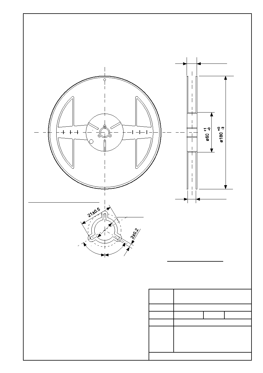
No.
TITLE
SCALE
UNIT
mm
Seiko Instruments Inc.
(60į)
(60į)
Ý13Ī0.2
12.5max.
9.0Ī0.3
QTY.
3,000
No. MP003-A-R-SD-1.1
MP003-A-R-SD-1.1
SOT233-A-Reel
Enlarged drawing in the central part

No.
TITLE
SCALE
UNIT
mm
Seiko Instruments Inc.
2.9Ī0.2
1.9Ī0.2
0.95Ī0.1
0.4Ī0.1
0.16
+0.1
-0.06
1
2
3
4
5
No. MP005-A-P-SD-1.2
MP005-A-P-SD-1.2
SOT235-A-PKG Dimensions
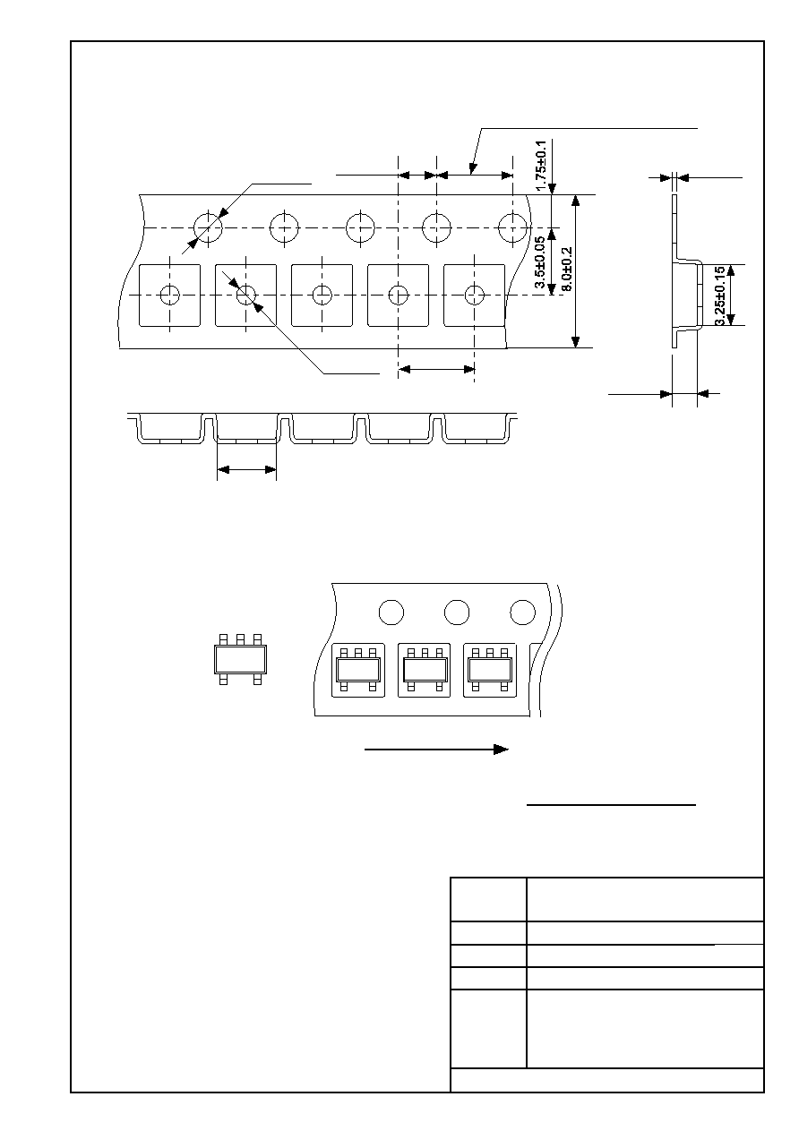
No.
TITLE
SCALE
UNIT
mm
Seiko Instruments Inc.
Ý1.5
+0.1
-0
2.0Ī0.05
Ý1.0
+0.2
-0
4.0Ī0.1
1.4Ī0.2
0.25Ī0.1
3.2Ī0.2
1
2
3
4
5
No. MP005-A-C-SD-2.1
MP005-A-C-SD-2.1
SOT235-A-Carrier Tape
Feed direction
4.0Ī0.1(10 pitches:40.0Ī0.2)

No.
TITLE
SCALE
UNIT
mm
Seiko Instruments Inc.
12.5max.
9.0Ī0.3
Ý13Ī0.2
(60į)
(60į)
QTY.
3,000
No. MP005-A-R-SD-1.1
MP005-A-R-SD-1.1
SOT235-A-Reel
Enlarged drawing in the central part

1.8Ī0.15
0.5Ī0.1
0.5Ī0.1
0.8Ī0.05
0.14Ī0.05
R(0.075)
0.2Ī0.08
(0.125)
1
2
3
4
5
6
SNB6B-A-PKG Dimensions
No. BD006-A-P-SD-1.1
Seiko Instruments Inc.
No.
TITLE
SCALE
UNIT
mm
BD006-A-P-SD-1.1
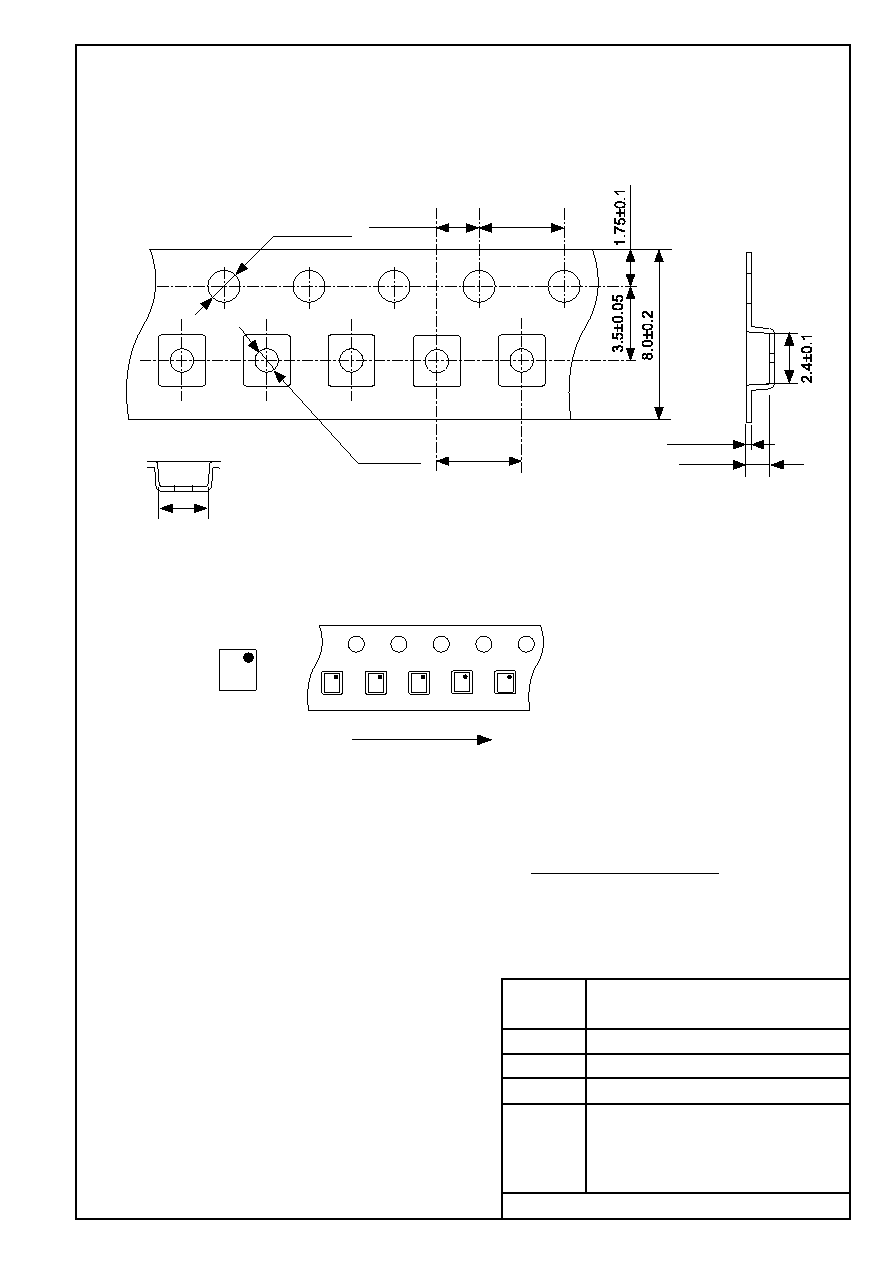
No.
TITLE
SCALE
UNIT
mm
4.0Ī0.1
2.0Ī0.05
4.0Ī0.1
Ý1.5Ī0.1
2.2Ī0.1
1.1Ī0.1
0.25Ī0.05
Ý1.1Ī0.1
Seiko Instruments Inc.
Feed direction
SNB6B-A-Carrier Tape
No. BD006-A-C-SD-2.1
BD006-A-C-SD-2.1
1
2
3
6
5
4

QTY.
3,000
No.
TITLE
SCALE
UNIT
mm
12.5max.
9.0Ī0.3
Ý13Ī0.2
Seiko Instruments Inc.
Enlarged drawing in the central part
SNB6B-A-Reel
No. BD006-A-R-SD-1.1
BD006-A-R-SD-1.1

∑
The information described herein is subject to change without notice.
∑
Seiko Instruments Inc. is not responsible for any problems caused by circuits or diagrams described herein
whose related industrial properties, patents, or other rights belong to third parties. The application circuit
examples explain typical applications of the products, and do not guarantee the success of any specific
mass-production design.
∑
When the products described herein are regulated products subject to the Wassenaar Arrangement or other
agreements, they may not be exported without authorization from the appropriate governmental authority.
∑
Use of the information described herein for other purposes and/or reproduction or copying without the
express permission of Seiko Instruments Inc. is strictly prohibited.
∑
The products described herein cannot be used as part of any device or equipment affecting the human
body, such as exercise equipment, medical equipment, security systems, gas equipment, or any apparatus
installed in airplanes and other vehicles, without prior written permission of Seiko Instruments Inc.
∑
Although Seiko Instruments Inc. exerts the greatest possible effort to ensure high quality and reliability, the
failure or malfunction of semiconductor products may occur. The user of these products should therefore
give thorough consideration to safety design, including redundancy, fire-prevention measures, and
malfunction prevention, to prevent any accidents, fires, or community damage that may ensue.