
Seiko Instruments Inc.
TABLE OF
CONTENTS
Part I
S-75V Series [High speed operation version]
S-75V00ANC
[Single 2-Input NAND Gate]
1
S-75V02ANC
[Single 2-Input NOR Gate]
4
S-75V04ANC [INVERTER]
7
S-75VU04ANC [Single INVERTER without Buffer]
10
S-75V08ANC
[Single 2-Input AND Gate]
13
S-75V14ANC [SCHMITT
INVERTER]
16
S-75V32ANC
[Single 2-Input OR Gate]
19
S-75V86ANC
[EXCLUSIVE OR GATE]
22
Part II
S-75L Series [Low voltage operation version]
S-75L00ANC
[Single 2-Input NAND Gate]
25
S-75L02ANC
[Single 2-Input NOR Gate]
28
S-75L04ANC [INVERTER]
31
S-75LU04ANC
[Single INVERTER without Buffer]
34
S-75L08ANC
[Single 2-Input AND Gate]
37
S-75L14ANC [SCHMITT
INVERTER]
40
S-75L32ANC
[Single 2-Input OR Gate]
43
S-75L86ANC
[EXCLUSIVE OR GATE]
46
SC-88A Package Specifications
Physical Dimensions
49
Taping Dimensions
49
Reel Dimensions
49
Rev. 1.1
_00
Seiko Instruments Inc.
1
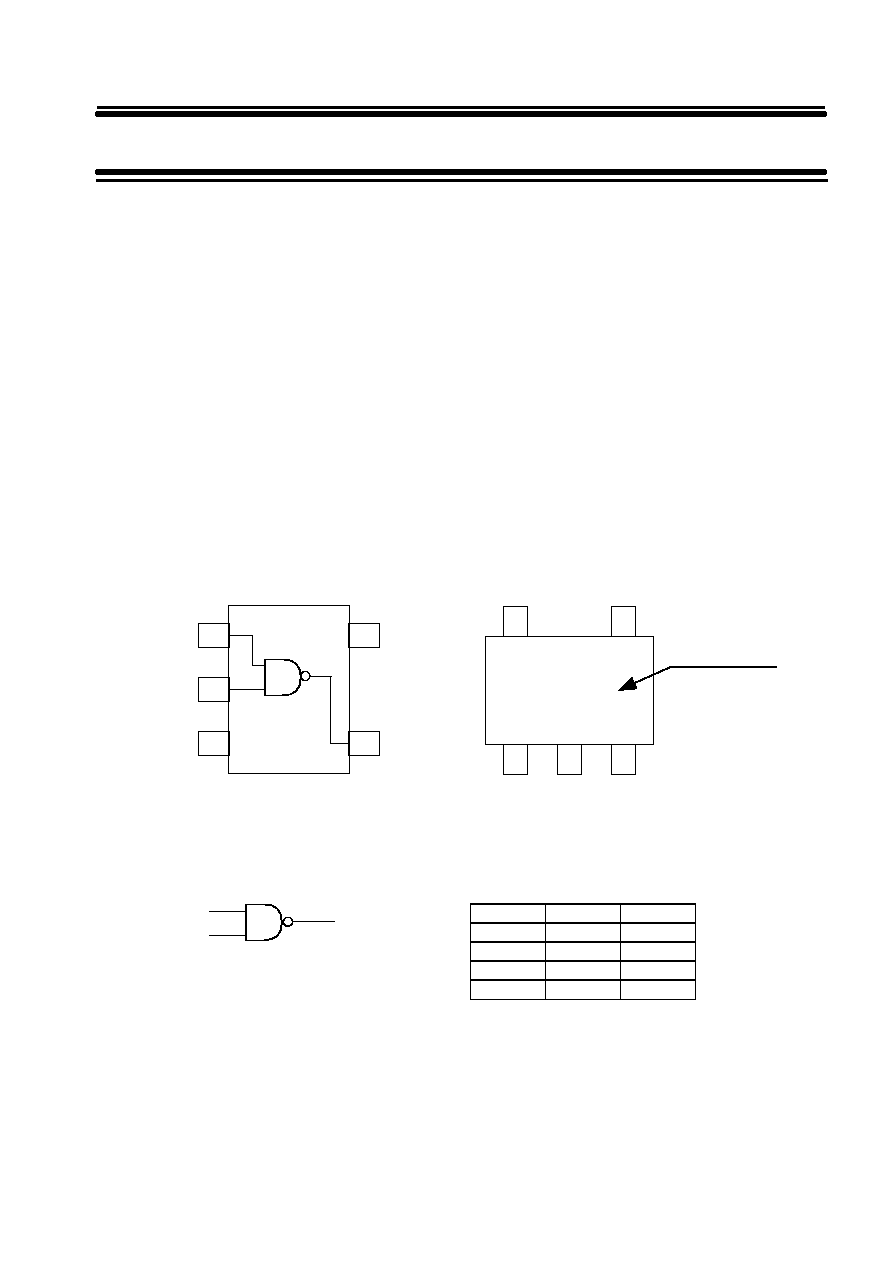
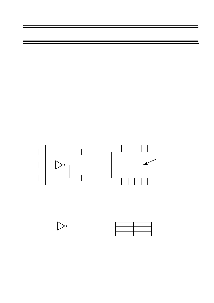
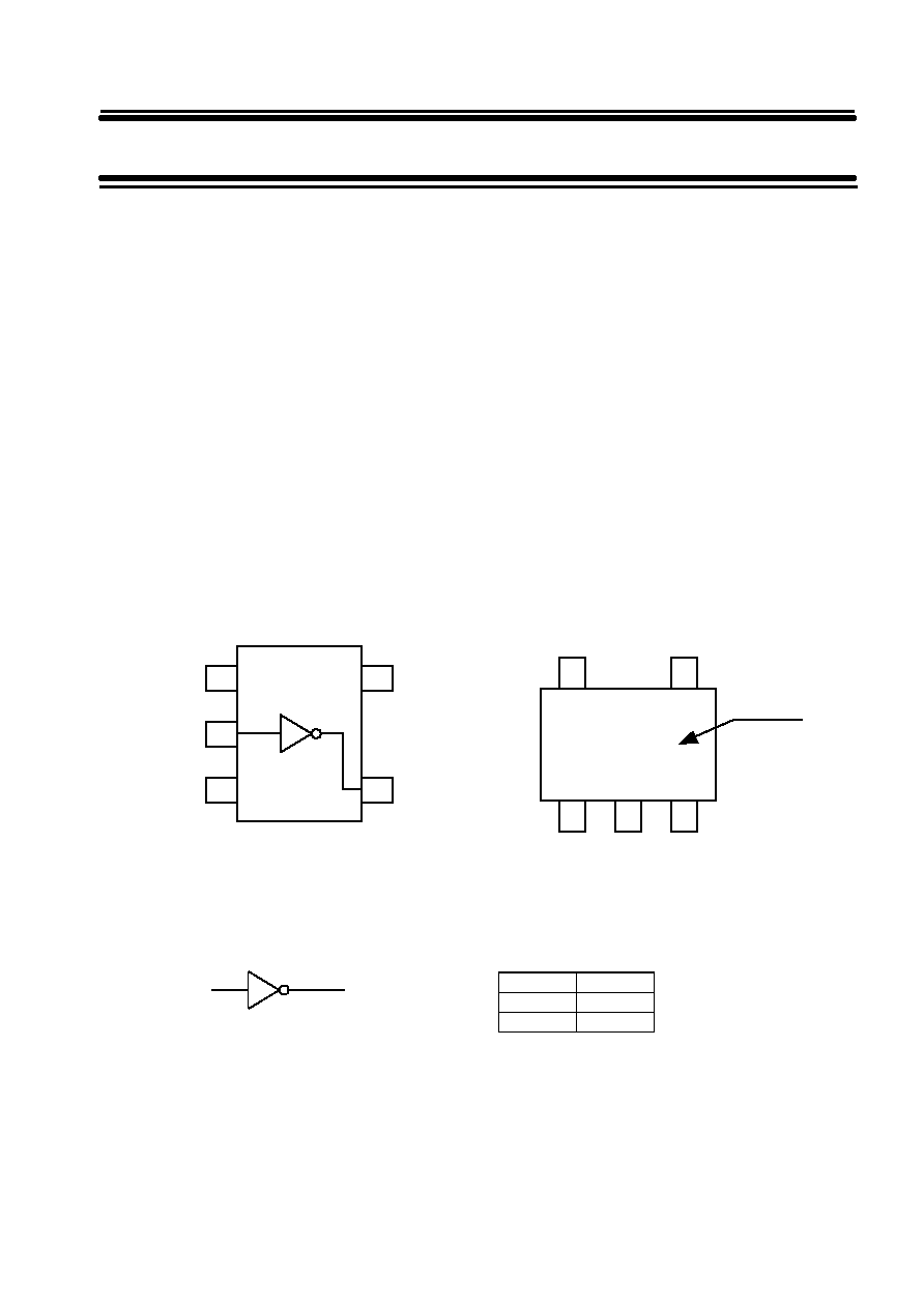
S-75V00ANC
Single 2-Input NAND Gate
The S-75V00ANC is a single 2-Input NAND Gate fabricated by utilizing
advanced silicon-gate CMOS technology which provides the inherent
benefit of CMOS low power consumption to achieve ultra high speed
operation correspond to LSTTL IC's.
All gates of the internal circuitry have buffered outputs to ensure high
noise immunity and output stability.
Input voltage is allowed to be applied even if power voltage is not supplied
because no diode is inserted between an input pin and V
CC
.
This allows for interfaces between power supplies of different voltage,
output level conversion from 5 V to 3 V and battery backup applications.
Features
Applications
∑ Wide power supply range: 2 V to 5.5 V
∑ Personal computers, peripherals
∑ Low current consumption: 1.0 µA max. (at 5.5 V, 25∞C)
∑ Cellular phones
∑ Typical propagation delay: tpd = 3.7 ns (at 5 V)
∑ Cameras
∑ High noise immunity:
V
NIH
=V
NIL
=28% V
CC
min.
∑ Games
∑ Power down protection:
All pins
∑ Very small plastic package: SC-88A
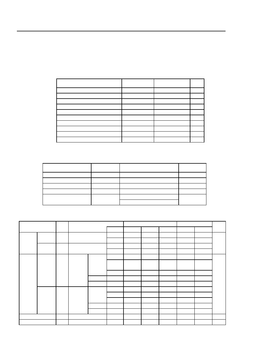
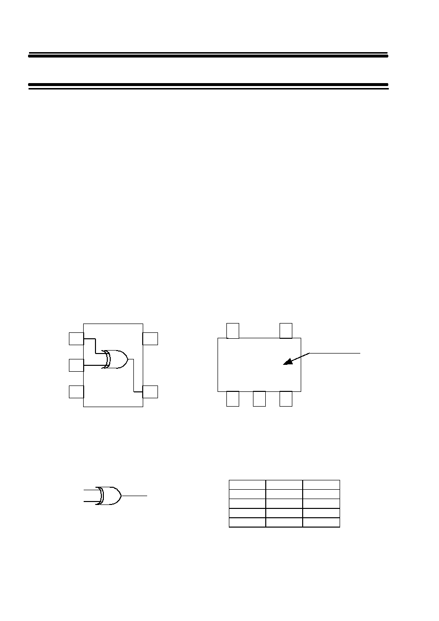
Pin Assignment
Marking
Logic Diagram
True Values
A B Y
L L H
L H H
H L H
H H L
3
2
1
4
(Top view)
5
5V1
OUT Y
1
IN B
IN A
GND
VCC
2
3
4
5
(Top view)
Model name
IN B
IN A
OUT Y
Miniaturized Logic IC Family
S-75V00ANC
Rev.1.1
_00
Seiko Instruments Inc.
2
Ordering
Delivery
form:
Taping
only
Model
name:
S-75V00ANC-5V1-TF
Absolute Maximum Ratings
Ta=25
∞C
Item Symbol
Ratings
Unit
Power Supply Voltage
V
CC
-0.5 to +7.0
V
Input Voltage
V
IN
-0.5 to +7.0
V
Output Voltage
V
OUT
-0.5 to V
CC
+0.5 V
Input Parasitic Diode Current
I
IK
-20 mA
Output Parasitic Diode Current
I
OK
±20 mA
Output Current
I
OUT
±25 mA
V
CC
/GND Current
I
CC
±50
mA
Power Dissipation
P
D
200
mW
Storage Temp. Range
Tstg
-65 to +150
∞C
Lead Temperature (10 sec.)
TL
260
∞C
Recommended Operating Conditions
Parameter Symbol
Standard
Unit
Power Voltage
V
CC
2 to 5.5
V
Input Voltage
V
IN
0 to 5.5
V
Output Voltage
V
OUT
0 to V
CC
V
Op. Temp. Range
Topr
-40 to +85
∞C
Input Rise and Fall Time
dt/dv
0 to 100 (V
CC
=3.3
±0.3V) ns/V
0 to 20 (V
CC
=5
±0. 5V)
DC Characteristics
Parameter
Sym.
Conditions Ta=25
∞C
Ta=-40 to 85
∞C
Unit
V
CC
MIN. TYP. MAX. MIN. MAX.
"H"
level
V
IH
2.0
1.5
1.5
Input
3 to 5.5
V
CC
X0.7
V
CC
X0.7
V
Voltage "L"
level V
IL
2.0
0.5 0.5
3 to 5.5
V
CC
X0.3
V
CC
X0.3
2.0
1.9
2.0
1.9
V
IN
=V
IL
I
OH
=-
50
µA
3.0 2.9 3.0
2.9
"H"
level
V
OH
or
V
IH
4.5
4.4 4.5
4.4
I
OH
=-4mA 3.0 2.58
2.48
Output I
OH
=-8mA 4.5 3.94
3.80 V
Voltage
2.0
0 0.1 0.1
I
OL
=50
µA 3.0
0 0.1 0.1
"L"
level
V
OL
V
IN
=V
IH
4.5
0 0.1 0.1
I
OL
=4mA 3.0
0.36 0.44
I
OL
=8mA 4.5
0.36 0.44
Input Current
I
IN
V
IN
=5.5V or GND
0 to 5.5
±0.1
±1.0
µA
Current Consump.
I
CC
V
IN
=V
CC
or GND
5.5
1.0 10.0
µA
Miniaturized Logic IC Family
Rev.1.1
_00
S-75V00ANC
Seiko Instruments Inc.
3
AC Characteristics
Input
t
r =
t
f = 3 ns (unless otherwise specified)
Parameter Sym.
Measurement
Conditions Ta=25
∞C
Ta=-40 to 85
∞C Unit
V
CC
(V)
C
L
(pF)
MIN. TYP. MAX. MIN. MAX.
3.3
±0.3
15
5.5
7.9
1.0
9.5
Output Rise/Fall time
t
pLH
50
10.0
14.0
1.0
15.0
nS
t
pHL
5.0
±0.5
15
3.7
5.5
1.0
6.5
50
6.1
8.5
1.0
9.0
Input Capacitance
C
IN
4
10
10
pF
Equiv. Int. Capacitance
C
PD
Note
1
14
pF
Note
1
C
PD
is the no-load equivalent capacitance inside the circuitry. Refer to the measurement circuit shown
below.
Current consumption is averaged by the following equation.
I
CC(opr)
=C
PD
V
CC
fin+I
CC
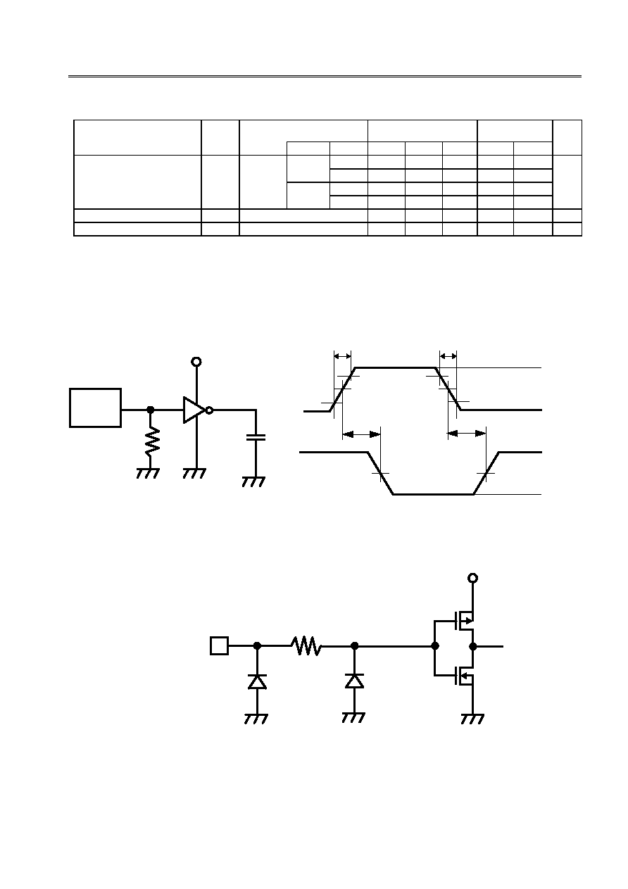
Measurement Circuit
VIN
CL
50
VOUT
PG
VOL
tp
LH
50%
50%
10%
90%
tp
HL
3ns
VIN
VOUT
3ns
GND
VCC
VOH
50%
Remark No-load output during measurement of current consumption.
Input Pin Equivalent Circuit
Input pin

Rev.1.1
_00
4
Seiko Instruments Inc.
S-75V02ANC
Single 2-Input NOR Gate
The S-75V02ANC is a single 2-intput NOR gate fabricated by utilizing
advanced silicon-gate CMOS technology which provides the inherent
benefit of CMOS low power consumption to achieve ultra high speed
operation correspond to LSTTL IC's.
All gates of the internal circuitry have buffered outputs to ensure high
noise immunity and output stability.
Input voltage is allowed to be applied even if power voltage is not supplied
because no diode is inserted between an input pin and V
CC
.
This allows for interfaces between power supplies of different voltage,
output level conversion from 5 V to 3 V and battery backup applications.
Features
Applications
∑ Wide power supply range: 2 V to 5.5 V
∑ Personal computers, peripherals
∑ Low current consumption: 1.0 µA max. (at 5.5 V, 25∞C)
∑ Cellular phones
∑ Typical propagation delay: tpd = 3.6 ns (at 5 V)
∑ Cameras
∑ High noise immunity:
V
NIH
=V
NIL
=28% V
CC
min.
∑ Games
∑ Power down protection:
All pins
∑ Very small plastic package: SC-88A
Pin Assignment
Marking
Logic Diagram
True Values
A B Y
L L H
L H L
H L L
H H L
Model name
3
2
1
4
(Top view)
5
5V3
1
IN B
IN A
GND
VCC
OUT Y
2
3
4
5
(Top view)
IN B
IN A
OUT Y

Miniaturized Logic IC Family
Rev.1.1
_00
S-75V02ANC
Seiko Instruments Inc.
5
Ordering
Delivery
form:
Taping
only
Model
name:
S-75V02ANC-5V3-TF
Absolute Maximum Ratings
Ta=25
∞C
Item Symbol
Ratings
Unit
Power Supply Voltage
V
CC
-0.5 to +7.0
V
Input Voltage
V
IN
-0.5 to +7.0
V
Output Voltage
V
OUT
-0.5 to V
CC
+0.5 V
Input Parasitic Diode Current
I
IK
-20 mA
Output Parasitic Diode Current
I
OK
±20 mA
Output Current
I
OUT
±25 mA
V
CC
/GND Current
I
CC
±50 mA
Power Dissipation
P
D
200 mW
Storage Temp. Range
Tstg
-65 to +150
∞C
Lead Temperature (10 sec.)
TL
260
∞C
Recommended Operating Conditions
Parameter
Symbol
Standard
Unit
Power Voltage
V
CC
2 to 5.5
V
Input Voltage
V
IN
0 to 5.5
V
Output Voltage
V
OUT
0 to V
CC
V
Op. Temp. Range
Topr
-40 to +85
∞C
Input Rise and Fall Time
dt/dv
0 to 100 (V
CC
=3.3
±0.3V) ns/V
0 to 20 (V
CC
=5
±0. 5V)
DC Characteristics
Parameter
Sym.
Conditions Ta=25
∞C
Ta=-40 to 85
∞C
Unit
V
CC
MIN. TYP. MAX. MIN. MAX.
"H"
level
V
IH
2.0
1.5
1.5
Input
3 to 5.5
V
CC
X0.7
V
CC
X0.7
V
Voltage "L"
level V
IL
2.0
0.5 0.5
3 to 5.5
V
CC
X0.3
V
CC
X0.3
2.0
1.9
2.0
1.9
I
OH
=-
50
µA
3.0 2.9 3.0
2.9
"H"
level
V
OH
V
IN
=V
IL
4.5 4.4 4.5
4.4
I
OH
=-4mA 3.0 2.58
2.48
Output I
OH
=-8mA 4.5 3.94
3.80 V
Voltage
2.0
0 0.1 0.1
V
IN
=V
IH
I
OL
=50
µA 3.0
0 0.1 0.1
"L"
level
V
OL
or
V
IL
4.5
0 0.1 0.1
I
OL
=4mA 3.0
0.36 0.44
I
OL
=8mA 4.5
0.36 0.44
Input Current
I
IN
V
IN
=5.5V or GND
0 to 5.5
±0.1
±1.0
µA
Current Consump.
I
CC
V
IN
=V
CC
or GND
5.5
1.0 10.0
µA
Miniaturized Logic IC Family
S-75V02ANC
Rev.1.1
_00
Seiko Instruments Inc.
6
AC Characteristics
Input
t
r =
t
f = 3 ns (unless otherwise specified)
Parameter Sym.
Measurement
Conditions Ta=25
∞C
Ta=-40 to 85
∞C Unit
V
CC
(V)
C
L
(pF)
MIN. TYP. MAX. MIN. MAX.
t
pLH
3.3
±0.3
15
5.6
7.9
1.0
9.5
Output Rise/Fall time
t
pHL
50
10.0
14.0
1.0
15.0
ns
5.0
±0.5
15
3.6
5.5
1.0
6.5
50
5.7
8.0
1.0
9.0
Input Capacitance
C
IN
4
10
10
pF
Equiv. Int. Capacitance
C
PD
Note
1
15
pF
Note
1
C
PD
is the no-load equivalent capacitance inside the circuitry. Refer to the measurement circuit shown
below.
Current consumption is averaged by the following equation.
I
CC(opr)
=C
PD
V
CC
fin+I
CC
Measurement Circuit
VIN
CL
50
VOUT
PG.
tp
LH
50%
50%
10%
90%
tp
HL
3ns
VIN
VOUT
3ns
GND
VCC
VOL
VOH
50%
Remark No-load output during measurement of current consumption.
Input Pin Equivalent Circuit
Input pin
Rev.1.1
_00
Seiko Instruments Inc.
7
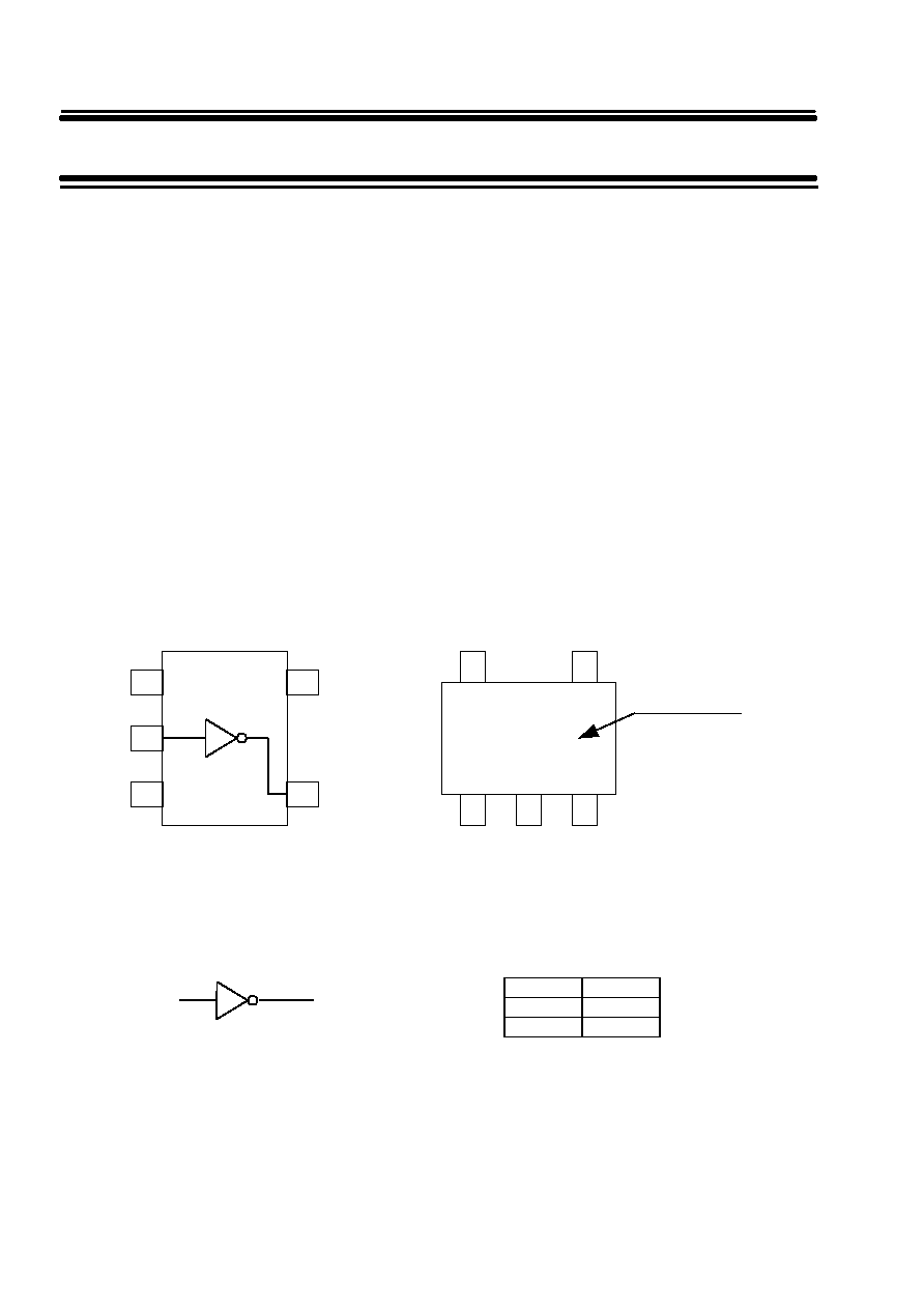
S-75V04ANC
INVERTER
The S-75V04ANC is a INVERTER fabricated by utilizing advanced silicon-
gate CMOS technology which provides the inherent benefit of CMOS low
power consumption to achieve ultra high speed operation correspond to
LSTTL IC's.
The special purpose unbuffered circuit design is suitable for a wide veriety
of linear circuits.
Input voltage is allowed to be applied even if power voltage is not supplied
because no diode is inserted between an input pin and V
CC
.
This allows for interfaces between power supplies of different voltage,
output level conversion from 5 V to 3 V and battery backup applications.
Features
Applications
∑ Wide power supply range: 2 V to 5.5 V
∑ Personal computers, peripherals
∑ Low current consumption: 1.0 µA max. (at 5.5 V, 25∞C)
∑ Cellular phones
∑ Typical propagation delay: tpd = 3.8 ns (at 5 V)
∑ Cameras
∑ High noise immunity:
V
NIH
=V
NIL
=28% V
CC
min.
∑ Games
∑ Power down protection:
All pins
∑ Very small plastic package: SC-88A
Pin Assignment
Marking
Logic Diagram
True Values
A Y
L H
H L
Model name
3
2
1
4
(Top view)
5
5V5
1
NC
IN A
GND
VCC
OUT Y
2
3
4
5
(Top view)
IN A
OUT Y
Miniaturized Logic IC Family
S-75V04ANC
Rev.1.1
_00
Seiko Instruments Inc.
8
Ordering
Delivery
form:
Taping
only
Model
name:
S-75V04ANC-5V5-TF
Absolute Maximum Ratings
Ta=25
∞C
Item Symbol
Ratings
Unit
Power Supply Voltage
V
CC
-0.5 to +7.0
V
Input Voltage
V
IN
-0.5 to +7.0
V
Output Voltage
V
OUT
-0.5 to V
CC
+0.5 V
Input Parasitic Diode Current
I
IK
-20 mA
Output Parasitic Diode Current
I
OK
±20 mA
Output Current
I
OUT
±25 mA
V
CC
/GND Current
I
CC
±50 mA
Power Dissipation
P
D
200 mW
Storage Temp. Range
Tstg
-65 to +150
∞C
Lead Temperature (10 sec.)
TL
260
∞C
Recommended Operating Conditions
Parameter Symbol Standard Unit
Power Voltage
V
CC
2 to 5.5
V
Input Voltage
V
IN
0 to 5.5
V
Output Voltage
V
OUT
0 to V
CC
V
Op. Temp. Range
Topr
-40 to +85
∞C
Input Rise and Fall Time
dt/dv
0 to 100 (V
CC
=3.3
±0.3V) ns/V
0 to 20 (V
CC
=5
±0.5V)
DC Characteristics
Parameter
Sym.
Conditions Ta=25
∞C
Ta=-40 to 85
∞C
Unit
V
CC
MIN. TYP. MAX. MIN. MAX.
"H"
level
V
IH
2.0
1.5
1.5
Input
3 to 5.5
V
CC
X0.7
V
CC
X0.7
V
Voltage "L"
level V
IL
2.0
0.5 0.5
3 to 5.5
V
CC
X0.3
V
CC
X0.3
2.0
1.9
2.0
1.9
I
OH
=-
50
µA
3.0 2.9 3.0
2.9
"H"
level
V
OH
V
IN
=V
IL
4.5 4.4 4.5
4.4
I
OH
=-4mA 3.0 2.58
2.48
Output I
OH
=-8mA 4.5 3.94
3.80 V
Voltage
2.0
0 0.1 0.1
I
OL
=50
µA 3.0
0 0.1 0.1
"L"
level
V
OL
V
IN
=V
IH
4.5
0 0.1 0.1
I
OL
=4mA 3.0
0.36 0.44
I
OL
=8mA 4.5
0.36 0.44
Input Current
I
IN
V
IN
=5.5V or GND
0 to 5.5
±0.1
±1.0
µA
Current Consump.
I
CC
V
IN
=V
CC
or GND
5.5
1.0 10.0
µA
Miniaturized Logic IC Family
Rev.1.1
_00
S-75V04ANC
Seiko Instruments Inc.
9
AC Characteristics
Input
t
r =
t
f = 3 ns (unless otherwise specified)
Parameter Sym.
Measurement
Conditions Ta=25
∞C
Ta=-40 to 85
∞C Unit
V
CC
(V)
C
L
(pF)
MIN. TYP. MAX. MIN. MAX.
t
pLH
3.3
±0.3
15
5.0
7.1
1.0
8.5
Output Rise/Fall time
t
pHL
50
9.6
13.5
1.0
14.5
ns
5.0
±0.5
15
3.8
5.5
1.0
6.5
50
5.7
8.0
1.0
9.0
Input Capacitance
C
IN
4
10
10
pF
Equiv. Int. Capacitance
C
PD
Note
1
13
pF
Note
1
C
PD
is the no-load equivalent capacitance inside the circuitry. Refer to the measurement circuit shown
below.
Current consumption is averaged by the following equation.
I
CC(opr)
=C
PD
V
CC
fin+I
CC
Measurement Circuit
VIN
CL
50
VOUT
PG
tp
LH
50%
50%
10%
90%
tp
HL
3ns
VIN
VOUT
3ns
GND
VCC
VOL
VOH
50%
Remark No-load output during measurement of current consumption.
Input pin Equivalent Circuit
Input pin

Rev.1.1
_00
10
Seiko Instruments Inc.
S-75VU04ANC
Single INVERTER without Buffer
The S-75VU04ANC is a inverter fabricated by utilizing advanced silicon-
gate CMOS technology which provides the inherent benefit of CMOS low
power consumption to achieve ultra high speed operation correspond to
LSTTL IC's.
The special purpose unbuffered circuit design is suitable for a wide variety
of linear circuits.
Input voltage is allowed to be applied even if power voltage is not supplied
because no diode is inserted between an input pin and V
CC
.
This allows for interfaces between power supplies of different voltage,
output level conversion from 5 V to 3 V and battery backup applications.
Features
Applications
∑ Wide power supply range: 2 V to 5.5 V
∑ Personal computers, peripherals
∑ Low current consumption: 1.0 µA max. (at 5.5 V, 25∞C)
∑ Cellular phones
∑ Typical propagation delay: tpd = 3.5 ns (at 5 V)
∑ Cameras
∑ High noise immunity:
V
NIH
=V
NIL
=10% V
CC
min.
∑ Games
∑ Power down protection:
All pins
∑ Very small plastic package: SC-88A
Pin Assignment
Marking
Logic Diagram
True Values
A Y
L H
H L
Model name
3
2
1
4
(Top view)
5
5V6
1
NC
IN A
GND
VCC
OUT Y
2
3
4
5
(Top view)
IN A
OUT Y
Miniaturized Logic IC Family
Rev.1.1
_00
S-75VU04ANC
Seiko Instruments Inc.
11
Ordering
Delivery
form:
Taping
only
Model
name:
S-75VU04ANC-5V6-TF
Absolute Maximum Ratings
Ta=25
∞C
Item Symbol
Ratings
Unit
Power Supply Voltage
V
CC
-0.5 to +7.0
V
Input Voltage
V
IN
-0.5 to +7.0
V
Output Voltage
V
OUT
-0.5 to V
CC
+0.5 V
Input Parasitic Diode Current
I
IK
-20 mA
Output Parasitic Diode Current
I
OK
±20 mA
Output Current
I
OUT
±25 mA
V
CC
/GND Current
I
CC
±50 mA
Power Dissipation
P
D
200 mW
Storage Temp. Range
Tstg
-65 to +150
∞C
Lead Temperature (10 sec.)
TL
260
∞C
Recommended Operating Conditions
Parameter Symbol
Standard
Unit
Power Voltage
V
CC
2 to 5.5
V
Input Voltage
V
IN
0 to 5.5
V
Output Voltage
V
OUT
0 to V
CC
V
Op. Temp. Range
Topr
-40 to +85
∞C
DC Characteristics
Parameter
Sym.
Conditions Ta=25
∞C
Ta=-40 to 85
∞C
Unit
V
CC
MIN. TYP. MAX. MIN. MAX.
"H"
level
V
IH
V
OUT
=V
OL
2.0
1.7
1.7
Input
3 to 5.5
V
CC
X0.8
V
CC
X0.8
V
Voltage "L"
level V
IL
V
OUT
=V
OH
2.0
0.3 0.3
3 to 5.5
V
CC
X0.2
V
CC
X0.2
2.0
1.8
2.0
1.8
V
IN
=V
IL
I
OH
=-
50
µA
3.0 2.7 3.0
2.7
"H"
level
V
OH
4.5 4.0 4.5
4.0
V
IN
= GND I
OH
=-4mA 3.0 2.58
2.48
Output I
OH
=-8mA 4.5 3.94
3.80 V
Voltage
2.0
0 0.2 0.2
V
IN
=V
IH
I
OL
=50
µA 3.0
0 0.3 0.3
"L"
level
V
OL
4.5
0 0.5 0.5
V
IN
= V
CC
I
OL
=4mA 3.0
0.36 0.44
I
OL
=8mA 4.5
0.36 0.44
Input Current
I
IN
V
IN
=5.5V or GND
0 to 5.5
±0.1
±1.0
µA
Current Consump.
I
CC
V
IN
=V
CC
or GND
5.5
1.0 10.0
µA
Miniaturized Logic IC Family
S-75VU04ANC
Rev.1.1
_00
Seiko Instruments Inc.
12
AC Characteristics
Input
t
r =
t
f = 3 ns (unless otherwise specified)
Parameter Sym.
Measurement
Conditions Ta=25
∞C
Ta=-40 to 85
∞C Unit
V
CC
(V)
C
L
(pF)
MIN. TYP. MAX. MIN. MAX.
t
pLH
3.3
±0.3
15
5.0
8.9
1.0
10.5
Output Rise/Fall time
t
pHL
50
8.9
12.5
1.0
13.5
ns
5.0
±0.5
15
3.5
5.5
1.0
6.5
50
5.4
7.5
1.0
8.0
Input Capacitance
C
IN
5
10
10
pF
Equiv. Int. Capacitance
C
PD
Note
1
6
pF
Note
1
C
PD
is the no-load equivalent capacitance inside the circuitry. Refer to the measurement circuit shown
below.
Current consumption is averaged by the following equation.
I
CC(opr)
=C
PD
V
CC
fin+I
CC
Measurement Circuit
VIN
CL
50
VOUT
PG
tp
LH
50%
50%
10%
90%
tp
HL
3ns
VIN
VOUT
3ns
GND
VCC
VOL
VOH
50%
Remark No-load output during measurement of current consumption.
Input Pin Equivalent Circuit
Input pin

Rev.1.1
_00
Seiko Instruments Inc.
13
S-75V08ANC
Single 2-Input AND Gate
The S-75V08ANC is a Single 2-Input AND Gate fabricated by utilizing
advanced silicon-gate CMOS technology which provides the inherent
benefit of CMOS low power consumption to achieve ultra high speed
operation correspond to LSTTL IC's.
All gates of the internal circuitry have buffered outputs to ensure high
noise immunity and output stability.
Input voltage is allowed to be applied even if power voltage is not supplied
because no diode is inserted between an input pin and V
CC
.
This allows for interfaces between power supplies of different voltage,
output level conversion from 5 V to 3 V and battery backup applications.
Features
Applications
∑ Wide power supply range: 2 V to 5.5 V
∑ Personal computers, peripherals
∑ Low current consumption: 1.0 µA max. (at 5.5 V, 25∞C)
∑ Cellular phones
∑ Typical propagation delay: tpd = 4.3 ns (at 5 V)
∑ Cameras
∑ High noise immunity:
V
NIH
=V
NIL
=28% V
CC
min.
∑ Games
∑ Power down protection:
All pins
∑ Very small plastic package: SC-88A
Pin Assignment
Marking
Logic Diagram
True Values
A B Y
L L L
L H L
H L L
H H H
Model name
3
2
1
4
(Top view)
5
5V2
IN B
GND
VCC
OUT Y
2
3
4
5
(Top view)
1
IN A
IN B
IN A
OUT Y

Miniaturized Logic IC Family
S-75V08ANC
Rev.1.1
_00
Seiko Instruments Inc.
14
Ordering
Delivery
form:
Taping
only
Model
name:
S-75V08ANC-5V2-TF
Absolute Maximum Ratings
Ta=25
∞C
Item Symbol
Ratings
Unit
Power Supply Voltage
V
CC
-0.5 to +7.0
V
Input Voltage
V
IN
-0.5 to +7.0
V
Output Voltage
V
OUT
-0.5 to V
CC
+0.5 V
Input Parasitic Diode Current
I
IK
-20 mA
Output Parasitic Diode Current
I
OK
±20 mA
Output Current
I
OUT
±25 mA
V
CC
/GND Current
I
CC
±50 mA
Power Dissipation
P
D
200 mW
Storage Temp. Range
Tstg
-65 to +150
∞C
Lead Temperature (10 sec.)
TL
260
∞C
Recommended Operating Conditions
Parameter
Symbol
Standard
Unit
Power Voltage
V
CC
2 to 5.5
V
Input Voltage
V
IN
0 to 5.5
V
Output Voltage
V
OUT
0 to V
CC
V
Op. Temp. Range
Topr
-40 to +85
∞C
Input Rise and Fall Time
dt/dv
0 to 100 (V
CC
=3.3
±0.3V) ns/V
0 to 20 (V
CC
=5
±0. 5V)
DC Characteristics
Parameter
Sym.
Conditions Ta=25
∞C
Ta=-40 to 85
∞C
Unit
V
CC
MIN. TYP. MAX. MIN. MAX.
"H"
level
V
IH
2.0
1.5
1.5
Input
3 to 5.5
V
CC
X0.7
V
CC
X0.7
V
Voltage "L"
level V
IL
2.0
0.5 0.5
3 to 5.5
V
CC
X0.3
V
CC
X0.3
2.0
1.9
2.0
1.9
I
OH
=-
50
µA
3.0 2.9 3.0
2.9
"H"
level
V
OH
V
IN
=V
IH
4.5 4.4 4.5
4.4
I
OH
=-4mA 3.0 2.58
2.48
Output I
OH
=-8mA 4.5 3.94
3.80 V
Voltage
2.0
0 0.1 0.1
I
OL
=50
µA 3.0
0 0.1 0.1
"L"
level
V
OL
V
IN
=V
IH
4.5
0 0.1 0.1
or
V
IL
I
OL
=4mA 3.0
0.36 0.44
I
OL
=8mA 4.5
0.36 0.44
Input Current
I
IN
V
IN
=5.5V or GND
0 to 5.5
±0.1
±1.0
µA
Current Consump.
I
CC
V
IN
=V
CC
or GND
5.5
1.0 10.0
µA

Miniaturized Logic IC Family
Rev.1.1
_00
S-75V08ANC
Seiko Instruments Inc.
15
AC Characteristics
Input
t
r =
t
f = 3 ns (unless otherwise specified)
Parameter Sym.
Measurement
Conditions Ta=25
∞C
Ta=-40 to 85
∞C Unit
V
CC
(V)
C
L
(pF)
MIN. TYP. MAX. MIN. MAX.
t
pLH
3.3
±0.3
15
6.2
8.8
1.0
10.5
Output Rise/Fall time
t
pHL
50
9.6
13.5
1.0
14.5
ns
5.0
±0.5
15
4.3
5.9
1.0
7.0
50
5.7
7.9
1.0
9.0
Input Capacitance
C
IN
4
10
10
pF
Equiv. Int. Capacitance
C
PD
Note
1
14
pF
Note
1
C
PD
is the no-load equivalent capacitance inside the circuitry. Refer to the measurement circuit shown
below.
Current consumption is averaged by the following equation.
I
CC(opr)
=C
PD
V
CC
fin+I
CC
Measurement Circuit
VIN
CL
50
VOUT
PG
tp
LH
50%
50%
10%
90%
tp
HL
3ns
VIN
VOUT
3ns
GND
VCC
VOL
VOH
50%
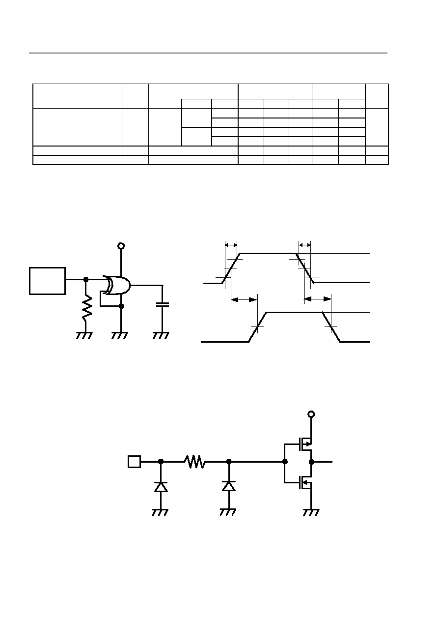
Remark No-load output during measurement of current consumption.
Input Pin Equivalent Circuit
Input pin

Rev.1.1
_00
16
Seiko Instruments Inc.
S-75V14ANC
SCHMITT INVERTER
The S-75V14ANC is a SCHMITT INVERTER fabricated by utilizing
advanced silicon-gate CMOS technology which provides the inherent
benefit of CMOS low power consumption to achieve ultra high speed
operation correspond to LSTTL IC's.
All gates of the internal circuitry have buffered outputs to ensure high
noise immunity and output stability.
Input voltage is allowed to be applied even if power voltage is not supplied
because no diode is inserted between an input pin and V
CC
.
This allows for interfaces between power supplies of different voltage,
output level conversion from 5 V to 3 V and battery backup applications.
Features
Applications
∑ Wide power supply range: 2 V to 5.5 V
∑ Personal computers, peripherals
∑ Low current consumption: 1.0 µA max. (at 5.5 V, 25∞C)
∑ Cellular phones
∑ Typical propagation delay: tpd = 5.5 ns (at 5 V)
∑ Cameras
∑ High noise immunity:
V
NIH
=V
NIL
=28% V
CC
min.
∑ Games
∑ Power down protection:
All pins
∑ Very small plastic package: SC-88A
Pin Assignment
Marking
Logic Diagram
True Values
A B
L H
H L
Model name
3
2
1
4
(Top view)
5
5VA
1
NC
IN A
GND
VCC
OUT Y
2
3
4
5
(Top view)
IN A
OUT Y
Miniaturized Logic IC Family
Rev.1.1
_00
S-75V14ANC
Seiko Instruments Inc.
17
Ordering
Delivery
form:
Taping
only
Model
name:
S-75V14ANC-5VA-TF
Absolute Maximum Ratings
Ta=25
∞C
Item Symbol
Ratings
Unit
Power Supply Voltage
V
CC
-0.5 to +7.0
V
Input Voltage
V
IN
-0.5 to +7.0
V
Output Voltage
V
OUT
-0.5 to V
CC
+0.5 V
Input Parasitic Diode Current
I
IK
-20 mA
Output Parasitic Diode Current
I
OK
±20 mA
Output Current
I
OUT
±25 mA
V
CC
/GND Current
I
CC
±50 mA
Power Dissipation
P
D
200 mW
Storage Temp. Range
Tstg
-65 to +150
∞C
Lead Temperature (10 sec.)
TL
260
∞C
Recommended Operating Conditions
Parameter Symbol
Standard
Unit
Power Voltage
V
CC
2 to 5.5
V
Input Voltage
V
IN
0 to 5.5
V
Output Voltage
V
OUT
0 to V
CC
V
Op. Temp. Range
Topr
-40 to +85
∞C
DC Characteristics
Parameter
Sym.
Conditions Ta=25
∞C
Ta=-40 to 85
∞C
Unit
V
CC
MIN. TYP. MAX. MIN. MAX.
3.0
2.20 2.20
"H"
level
V
P
4.5
3.15 3.15
Threshold
5.5
3.85 3.85 V
Voltage
3.0
0.90
0.90
"L"
level
V
N
4.5
1.35
1.35
5.5
1.65
1.65
3.0
0.30
1.20 0.30 1.20
Hysteresis V
H
4.5
0.40
1.40 0.40 1.40 V
5.5
0.5
1.60 0.5 1.60
2.0
1.9
2.0
1.9
I
OH
=-
50
µA
3.0 2.9 3.0
2.9
"H"
level
V
OH
V
IN
=V
IL
4.5 4.4 4.5
4.4
I
OH
=-4mA 3.0 2.58
2.48
Output I
OH
=-8mA 4.5 3.94
3.80 V
Voltage
2.0
0 0.1 0.1
I
OL
=50
µA 3.0
0 0.1 0.1
"L"
level
V
OL
V
IN
=V
IH
4.5
0 0.1 0.1
I
OL
=4mA 3.0
0.36 0.44
I
OL
=8mA 4.5
0.36 0.44
Input Current
I
IN
V
IN
=5.5V or GND
0 to 5.5
±0.1
±1.0
µA
Current Consump.
I
CC
V
IN
=V
CC
or GND
5.5
1.0 10.0
µA
Miniaturized Logic IC Family
S-75V14ANC
Rev.1.1
_00
Seiko Instruments Inc.
18
AC Characteristics
Input
t
r =
t
f = 3 ns (unless otherwise specified)
Parameter Sym.
Measurement
Conditions Ta=25
∞C
Ta=-40 to 85
∞C Unit
V
CC
(V)
C
L
(pF)
MIN. TYP. MAX. MIN. MAX.
t
pLH
3.3
±0.3
15
8.3
12.8
1.0
15.0
Output Rise/Fall Time
t
pHL
50
10.8
16.3
1.0
18.5
ns
5.0
±0.5
15
5.5
8.6
1.0
10.0
50
7.0
10.6
1.0
12.0
Input Capacitance
C
IN
4
10
10
pF
Equiv. Int. Capacitance
C
PD
Note
1
14
pF
Note
1
C
PD
is the no-load equivalent capacitance inside the circuitry. Refer to the measurement circuit shown
below.
Current consumption is averaged by the following equation.
I
CC(opr
)
=C
PD
V
CC
fin+I
CC
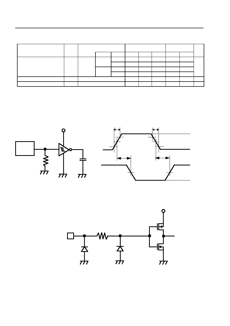
Measurement Circuit
VIN
CL
50
VOUT
PG.
tp
LH
50%
50%
10%
90%
tp
HL
3ns
VIN
VOUT
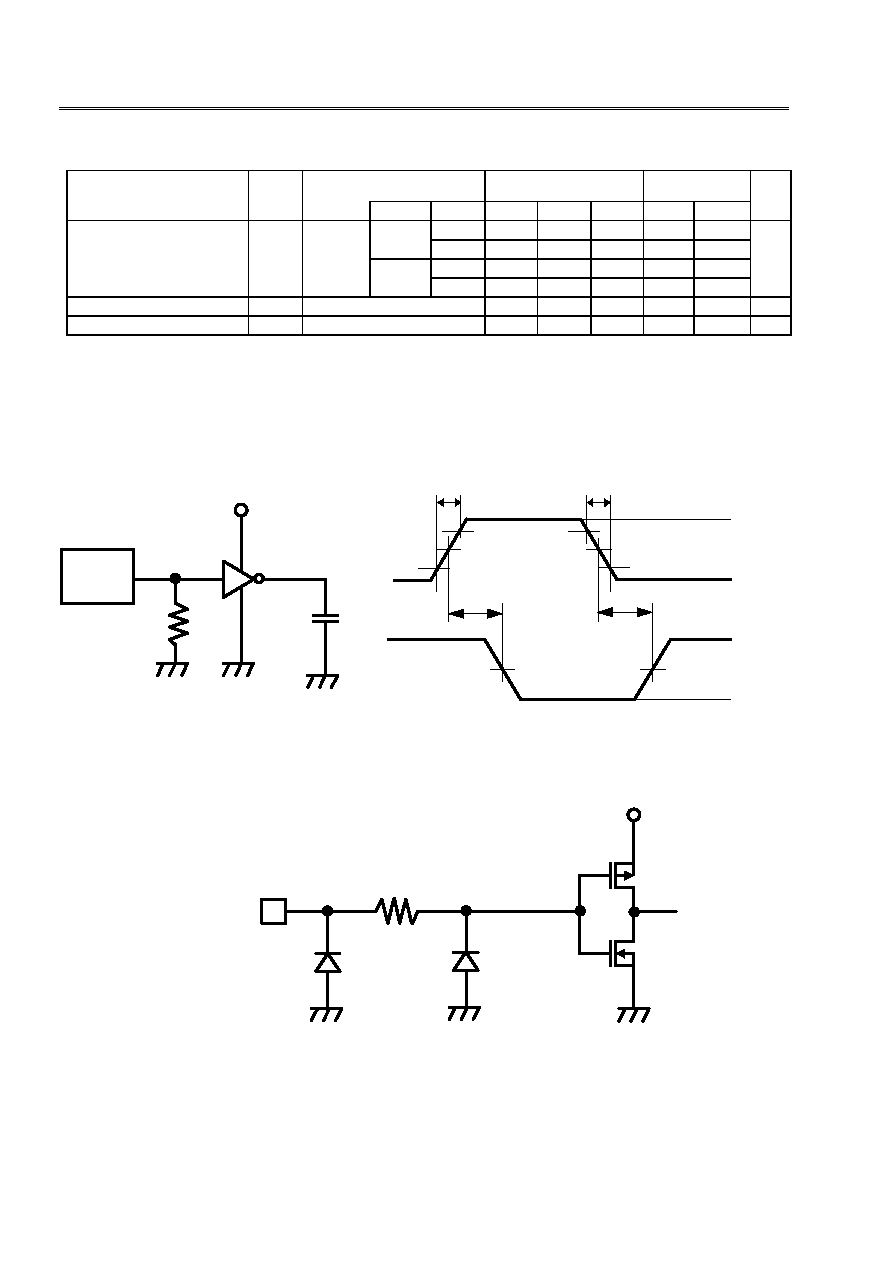
3ns
GND
VCC
VOL
VOH
50%
Remark No-load output during measurement of current consumption.
Input Pin Equivalent Circuit
Input pin
Rev.1.1
_00
Seiko Instruments Inc.
19
S-75V32ANC
Single 2-Input OR Gate
The S-75V32ANC is a single 2-intput OR gate fabricated by utilizing
advanced silicon-gate CMOS technology which provides the inherent
benefit of CMOS low power consumption to achieve ultra high speed
operation correspond to LSTTL IC's.
All gates of the internal circuitry have buffered outputs to ensure high
noise immunity and output stability.
Input voltage is allowed to be applied even if power voltage is not supplied
because no diode is inserted between an input pin and V
CC
.
This allows for interfaces between power supplies of different voltage,
output level conversion from 5 V to 3 V and battery backup applications.
Features
Applications
∑ Wide power supply range: 2 V to 5.5 V
∑ Personal computers, peripherals
∑ Low current consumption: 1.0 µA max. (at 5.5 V, 25∞C)
∑ Cellular phones
∑ Typical propagation delay: tpd = 3.8 ns (at 5 V)
∑ Cameras
∑ High noise immunity:
V
NIH
=V
NIL
=28% V
CC
min.
∑ Games
∑ Power down protection:
All pins
∑ Very small plastic package: SC-88A
Pin Assignment
Marking
Logic Diagram
True Values
A B Y
L L L
L H H
H L H
H H H
Model name
3
2
1
4
(Top view)
5
5V4
1
IN B
IN A
GND
VCC
OUT Y
2
3
4
5
(Top view)
IN B
IN A
OUT Y
Miniaturized Logic IC Family
S-75V32ANC
Rev.1.1
_00
Seiko Instruments Inc.
20
Ordering
Delivery
form:
Taping
only
Model
name:
S-75V32ANC-5V4-TF
Absolute Maximum Ratings
Ta=25
∞C
Item Symbol
Ratings
Unit
Power Supply Voltage
V
CC
-0.5 to +7.0
V
Input Voltage
V
IN
-0.5 to +7.0
V
Output Voltage
V
OUT
-0.5 to V
CC
+0.5 V
Input Parasitic Diode Current
I
IK
-20 mA
Output Parasitic Diode Current
I
OK
±20 mA
Output Current
I
OUT
±25 mA
V
CC
/GND Current
I
CC
±50 mA
Power Dissipation
P
D
200 mW
Storage Temp. Range
Tstg
-65 to +150
∞C
Lead Temperature (10 sec.)
TL
260
∞C
Recommended Operating Conditions
Parameter
Symbol
Standard
Unit
Power Voltage
V
CC
2 to 5.5
V
Input Voltage
V
IN
0 to 5.5
V
Output Voltage
V
OUT
0 to V
CC
V
Op. Temp. Range
Topr
-40 to +85
∞C
Input Rise and Fall Time
dt/dv
0 to 100 (V
CC
=3.3
±0.3V) ns/V
0 to 20 (V
CC
=5
±0. 5V)
DC Characteristics
Parameter
Sym.
Conditions Ta=25
∞C
Ta=-40 to 85
∞C
Unit
V
CC
MIN. TYP. MAX. MIN. MAX.
"H"
level
V
IH
2.0
1.5
1.5
Input
3 to 5.5
V
CC
X0.7
V
CC
X0.7
V
Voltage "L"
level V
IL
2.0
0.5 0.5
3 to 5.5
V
CC
X0.3
V
CC
X0.3
2.0
1.9
2.0
1.9
V
IN
=V
IL
I
OH
=-
50
µA
3.0 2.9 3.0
2.9
"H"
level
V
OH
or
V
IH
4.5
4.4 4.5
4.4
I
OH
=-4mA 3.0 2.58
2.48
Output I
OH
=-8mA 4.5 3.94
3.80 V
Voltage
2.0
0 0.1 0.1
I
OL
=50
µA 3.0
0 0.1 0.1
"L"
level
V
OL
V
IN
=V
IL
4.5
0 0.1 0.1
I
OL
=4mA 3.0
0.36 0.44
I
OL
=8mA 4.5
0.36 0.44
Input Current
I
IN
V
IN
=5.5V or GND
0 to 5.5
±0.1
±1.0
µA
Current Consump.
I
CC
V
IN
=V
CC
or GND
5.5
1.0 10.0
µA

Miniaturized Logic IC Family
Rev.1.1
_00
S-75V32ANC
Seiko Instruments Inc.
21
AC Characteristics
Input
t
r =
t
f = 3 ns (unless otherwise specified)
Parameter Sym.
Measurement
Conditions Ta=25
∞C
Ta=-40 to 85
∞C Unit
V
CC
(V)
C
L
(pF)
MIN. TYP. MAX. MIN. MAX.
t
pLH
3.3
±0.3
15
5.5
7.9
1.0
9.5
Output Rise/Fall time
t
pHL
50
10.0
14.0
1.0
15.0
ns
5.0
±0.5
15
3.8
5.5
1.0
6.5
50
6.1
8.5
1.0
9.0
Input Capacitance
C
IN
4
10
10
pF
Equiv. Int. Capacitance
C
PD
Note
1
15
pF
Note
1
C
PD
is the no-load equivalent capacitance inside the circuitry. Refer to the measurement circuit shown
below.
Current consumption is averaged by the following equation.
I
CC(opr)
=C
PD
V
CC
fin+I
CC
Measurement Circuit
VIN
CL
50
VOUT
PG
tp
LH
50%
50%
10%
90%
tp
HL
3ns
VIN
VOUT
3ns
GND
VCC
VOL
VOH
50%
Remark No-load output during measurement of current consumption.
Input Pin Equivalent Circuit
Input pin
Rev.1.1
_00
22
Seiko Instruments Inc.
S-75V86ANC
EXCLUSIVE OR GATE
The S-75V86ANC is a EXCLUSIVE OR GATE fabricated by utilizing
advanced silicon-gate CMOS technology which provides the inherent
benefit of CMOS low power consumption to achieve ultra high speed
operation correspond to LSTTL IC's.
All gates of the internal circuitry have buffered outputs to ensure high
noise immunity and output stability.
Input voltage is allowed to be applied even if power voltage is not supplied
because no diode is inserted between an input pin and V
CC
.
This allows for interfaces between power supplies of different voltage,
output level conversion from 5 V to 3 V and battery backup applications.
Features
Applications
∑ Wide power supply range: 2 V to 5.5 V
∑ Personal computers, peripherals
∑ Low current consumption: 1.0 µA max. (at 5.5 V, 25∞C)
∑ Cellular phones
∑ Typical propagation delay: tpd = 4.8 ns (at 5 V)
∑ Cameras
∑ High noise immunity:
V
NIH
=V
NIL
=28% V
CC
min.
∑ Games
∑ Power down protection:
All pins
∑ Very small plastic package: SC-88A
Pin Assignment
Marking
Logic Diagram
True Values
A B Y
L L L
L H H
H L H
H H L
Model name
3
2
1
4
(Top view)
5
5V8
1
IN B
IN A
GND
VCC
OUT Y
2
3
4
5
(Top view)
IN B
IN A
OUT Y
Miniaturized Logic IC Family
Rev.1.1
_00
S-75V86ANC
Seiko Instruments Inc.
23
Ordering
Delivery
form:
Taping
only
Model
name:
S-75V86ANC-5V8-TF
Absolute Maximum Ratings
Ta=25
∞C
Item Symbol
Ratings
Unit
Power Supply Voltage
V
CC
-0.5 to +7.0
V
Input Voltage
V
IN
-0.5 to +7.0
V
Output Voltage
V
OUT
-0.5 to V
CC
+0.5 V
Input Parasitic Diode Current
I
IK
-20 mA
Output Parasitic Diode Current
I
OK
±20 mA
Output Current
I
OUT
±25 mA
V
CC
/GND Current
I
CC
±50 mA
Power Dissipation
P
D
200 mW
Storage Temp. Range
Tstg
-65 to +150
∞C
Lead Temperature (10 sec.)
TL
260
∞C
Recommended Operating Conditions
Parameter
Symbol
Standard
Unit
Power Voltage
V
CC
2 to 5.5
V
Input Voltage
V
IN
0 to 5.5
V
Output Voltage
V
OUT
0 to V
CC
V
Op. Temp. Range
Topr
-40 to +85
∞C
0 to 100 (V
CC
=3.3
±0.3V)
0 to 20 (V
CC
=5
±0. 5V)
DC Characteristics
Parameter
Sym.
Conditions Ta=25
∞C
Ta=-40 to 85
∞C
Unit
V
CC
MIN. TYP. MAX. MIN. MAX.
"H"
level
V
IH
2.0
1.5
1.5
Input
3 to 5.5
V
CC
X0.7
V
CC
X0.7
V
Voltage "L"
level V
IL
2.0
0.5 0.5
3 to 5.5
V
CC
X0.3
V
CC
X0.3
2.0
1.9
2.0
1.9
V
IN
=V
IL
I
OH
=-
50
µA
3.0 2.9 3.0
2.9
"H"
level
V
OH
or
V
IH
4.5
4.4 4.5
4.4
I
OH
=-4mA 3.0 2.58
2.48
Output I
OH
=-8mA 4.5 3.94
3.80 V
Voltage
2.0
0 0.1 0.1
V
IN
=V
IL
I
OL
=50
µA 3.0
0 0.1 0.1
"L"
level
V
OL
or
V
IH
4.5
0 0.1 0.1
I
OL
=4mA 3.0
0.36 0.44
I
OL
=8mA 4.5
0.36 0.44
Input Current
I
IN
V
IN
=5.5V or GND
0 to 5.5
±0.1
±1.0
µA
Current Consump.
I
CC
V
IN
=V
CC
or GND
5.5
1.0 10.0
µA
Input Rise and Fall Time
ns/V
dt/dv
Miniaturized Logic IC Family
S-75V86ANC
Rev.1.1
_00
Seiko Instruments Inc.
24
AC Characteristics
Input
t
r =
t
f = 3 ns (unless otherwise specified)
Parameter Sym.
Measurement
Conditions Ta=25
∞C
Ta=-40 to 85
∞C Unit
V
CC
(V)
C
L
(pF)
MIN. TYP. MAX. MIN. MAX.
t
pLH
3.3
±0.3
15
7.0
11.0
1.0
13.0
Output Rise/Fall Time
t
pHL
50
10.4
14.5
1.0
16.5
ns
5.0
±0.5
15
4.8
6.8
1.0
8.0
50
6.5
9.0
1.0
10.0
Input Capacitance
C
IN
4
10
10
pF
Equiv. Int. Capacitance
C
PD
Note
1
18
pF
Note
1
C
PD
is the no-load equivalent capacitance inside the circuitry. Refer to the measurement circuit shown
below.
Current consumption is averaged by the following equation.
I
CC(opr)
=C
PD
V
CC
fin+I
CC
Measurement Circuit
VIN
CL
50
VOUT
PG
tp
LH
50%
50%
10%
90%
tp
HL
3ns
VIN
VOUT
3ns
GND
VCC
VOL
VOH
50%
Remark No-load output during measurement of current consumption.
Input Pin Equivalent Circuit
Input pin

Rev.1.1
_00
Seiko Instruments Inc.
25
S-75L00ANC
Single 2-Input NAND Gate
The S-75L00ANC is a single 2-intput NAND gate fabricated by utilizing
advanced silicon-gate CMOS technology which provides the inherent
benefit of CMOS low power consumption to achieve operation by only a
couple of batteries (1 to 3V).
The internal circuitry has buffered outputs to ensure high noise immunity
and output stability.
Input voltage is allowed to be applied even if power voltage is not supplied
because no diode is inserted between an input pin and V
CC
.
This allows for interfaces between power supplies of different voltage,
output level conversion from 3 V to 1 V and battery backup applications.
Features
Applications
∑ Wide power supply range: 1 V to 3.6 V
∑ Personal computers, peripherals
∑ Low current consumption: 1.0 µA max. (at 3.6 V, 25∞C)
∑ Cellular phones
∑ Typical propagation delay: tpd = 7 ns (at 3.0 V)
∑ Cameras
∑ High noise immunity:
V
NIH
=V
NIL
=28% V
CC
min.
∑ Games
∑ Power down protection:
All pins
∑ Very small plastic package: SC-88A
Pin Assignment
Marking
Logic Diagram
True Values
A B Y
L L H
L H H
H L H
H H L
3
2
1
4
(Top view)
5
5L1
OUT Y
1
IN B
IN A
GND
VCC
2
3
4
5
(Top view)
Model name
IN B
IN A
OUT Y
Miniaturized Logic IC Family
S-75L00ANC
Rev.1.1
_00
Seiko Instruments Inc.
26
Ordering
Delivery
form:
Taping
only
Model
name:
S-75L00ANC-5L1-TF
Absolute Maximum Ratings
Ta=25
∞C
Item Symbol
Ratings
Unit
Power Supply Voltage
V
CC
-0.5 to +5.0
V
Input Voltage
V
IN
-0.5 to +5.0
V
Output Voltage
V
OUT
-0.5 to V
CC
+0.5 V
Input Parasitic Diode Current
I
IK
-20 mA
Output Parasitic Diode Current
I
OK
±20 mA
Output Current
I
OUT
±12.5 mA
V
CC
/GND Current
I
CC
±25
mA
Power Dissipation
P
D
200
mW
Storage Temp. Range
Tstg
-65 to +150
∞C
Lead Temperature (10 sec.)
TL
260
∞C
Recommended Operating Conditions
Parameter
Symbol
Standard
Unit
Power Voltage
V
CC
1 to 3.6
V
Input Voltage
V
IN
0 to 3.6
V
Output Voltage
V
OUT
0 to V
CC
V
Op. Temp. Range
Topr
-40 to +85
∞C
0 to 1000 (V
CC
=1.0 V)
Input Rise and Fall Time
dt/dv
0 to 500 (V
CC
=2.0 V)
ns
0 to 400 (V
CC
=3.0 V)
DC Characteristics
Parameter
Sym.
Conditions Ta=25
∞C
Ta=-40 to 85
∞C
Unit
V
CC
MIN. TYP. MAX. MIN. MAX.
1.0
0.75
0.75
"H"
level
V
IH
1.5
1.05
1.05
Input
3.0
2.10
2.10 V
Voltage
1.0
0.25 0.25
"L"
level
V
IL
1.5
0.45 0.45
3.0
0.90 0.90
1.0
0.9
1.0
0.9
V
IN
=V
I
H
I
OH
=-20
µA 1.5 1.4 1.5
1.4
"H"
level
V
OH
or
V
IL
3.0 2.9 3.0
2.9
I
OH
=-1mA 1.5 1.07 1.23
0.99
Output I
OH
=-
2.6mA
3.0 2.61 2.68
2.55 V
Voltage
1.0
0 0.1 0.1
I
OL
=20
µA 1.5 0 0.1 0.1
"L"
level
V
OL
V
IN
=V
I
H
3.0
0 0.1 0.1
I
OL
=1mA 1.5
0.23 0.31 0.37
I
OL
=2.6mA 3.0
0.23 0.31 0.33
Input Current
I
IN
V
IN
=V
CC
or GND
3.6
±0.1
±1.0
µA
Current Consump.
I
CC
V
IN
=V
CC
or GND
3.6
1.0 10.0
µA

Miniaturized Logic IC Family
Rev.1.1
_00
S-75L00ANC
Seiko Instruments Inc.
27
AC Characteristics
C
L
=15pf, Input tr=tf=6ns, V
CC
=3.3
±0.3V, Ta=25
∞C (unless otherwise specified)
Parameter Sym.
Measurement
Conditions
MIN.
TYP.
MAX.
Unit
Output Rise/Fall Time
t
TLH,
t
THL
4.0 8.5
Propagation Delay Time
t
pLH,
t
pHL
6.0 9.0
C
L
=25pf, Input tr=tf=6ns
(unless otherwise specified)
Parameter Sym.
Measurement
Conditions Ta=25
∞C
Ta=-40 to 85
∞C
Unit
V
CC
(V)
Min. Typ. Max. Min. Max.
Output Rise/Fall
t
TLH
1.0
35 70 90
Time t
THL
1.5
15 25 30
3.0
7 10 14 ns
Propagation
t
pLH
1.0
30 60 75
Delay Time
t
pHL
1.5
15 25 30
3.0
7 10 14
Input Capacitance
C
IN
5 10 10 pF
Equiv.Int. Capacitance
C
PD
Note
1
10
pF
Note
1
C
PD
is the no-load equivalent capacitance inside the circuitry. Refer to the measurement circuit shown
below.
Current consumption is averaged by the following equation.
I
CC(opr)
=C
PD
V
CC
fin+
I
CC
Measurement Circuit
VIN
CL
50
VOUT
PG
VOL
tp
LH
50%
50%
10%
90%
tp
HL
6ns
VIN
VOUT
6ns
GND
VCC
VOH
50%
Remark No-load output during measurement of current consumption.
Input Pin Equivalent Circuit
Input pin
ns

Rev.1.1
_00
28
Seiko Instruments Inc.
S-75L02ANC
Single 2-Input NOR Gate
The S-75L02ANC is a single 2-intput NOR gate fabricated by utilizing
advanced silicon-gate CMOS technology which provides the inherent
benefit of CMOS low power consumption to achieve operation by only a
couple of batteries (1 to 3V).
The internal circuitry has buffered outputs to ensure high noise immunity
and output stability.
Input voltage is allowed to be applied even if power voltage is not supplied
because no diode is inserted between an input pin and V
CC
.
This allows for interfaces between power supplies of different voltage,
output level conversion from 3 V to 1 V and battery backup applications.
Features
Applications
∑ Wide power supply range: 1 V to 3.6 V
∑ Personal computers, peripherals
∑ Low current consumption: 1.0 µA max. (at 3.6 V, 25∞C)
∑ Cellular phones
∑ Typical propagation delay: tpd = 7 ns (at 3 V)
∑ Cameras
∑ High noise immunity:
V
NIH
=V
NIL
=28% V
CC
min.
∑ Games
∑ Power down protection:
All pins
∑ Very small plastic package: SC-88A
Pin Assignment
Marking
Logic Diagram
True Values
A B Y
L L H
L H L
H L L
H H L
Model name
3
2
1
4
(Top view)
5
5L3
1
IN B
IN A
GND
VCC
OUT Y
2
3
4
5
(Top view)
IN B
IN A
OUT Y

Miniaturized Logic IC Family
Rev.1.1
_00
S-75L02ANC
Seiko Instruments Inc.
29
Ordering
Delivery
form:
Taping
only
Model
name:
S-75L02ANC-5L3-TF
Absolute Maximum Ratings
Ta=25
∞C
Item Symbol
Ratings
Unit
Power Supply Voltage
V
CC
-0.5 to +5.0
V
Input Voltage
V
IN
-0.5 to +5.0
V
Output Voltage
V
OUT
-0.5 to V
CC
+0.5 V
Input Parasitic Diode Current
I
IK
-20 mA
Output Parasitic Diode Current
I
OK
±20 mA
Output Current
I
OUT
±12.5 mA
V
CC
/GND Current
I
CC
±25
mA
Power Dissipation
P
D
200
mW
Storage Temp. Range
Tstg
-65 to +150
∞C
Lead Temperature (10 sec.)
TL
260
∞C
Recommended Operating Conditions
Parameter
Symbol
Standard
Unit
Power Voltage
V
CC
1 to 3.6
V
Input Voltage
V
IN
0 to 3.6
V
Output Voltage
V
OUT
0 to V
CC
V
Op. Temp. Range
Topr
-40 to +85
∞C
0 to 1000 (V
CC
=1.0 V)
Input Rise and Fall Time
dt/dv
0 to 500 (V
CC
=2.0 V)
ns
0 to 400 (V
CC
=3.0 V)
DC Characteristics
Parameter
Sym.
Conditions Ta=25
∞C
Ta=-40 to 85
∞C
Unit
V
CC
MIN. TYP. MAX. MIN. MAX.
1.0
0.75
0.75
"H"
level
V
IH
1.5
1.05
1.05
Input
3.0
2.10
2.10 V
Voltage
1.0
0.25 0.25
"L"
level
V
IL
1.5
0.45 0.45
3.0
0.90 0.90
1.0
0.9
1.0
0.9
V
IN
=V
IL
I
OH
=-20
µA 1.5 1.4 1.5
1.4
"H"
level
V
OH
3.0 2.9 3.0
2.9
I
OH
=-1mA 1.5 1.07 1.23
0.99
Output I
OH
=-
2.6mA
3.0 2.61 2.68
2.55 V
Voltage
1.0
0 0.1 0.1
I
OL
=20
µA 1.5 0 0.1 0.1
"L"
level
V
OL
V
IN
=V
IL
3.0
0 0.1 0.1
or
V
IH
I
OL
=1mA 1.5
0.23 0.31 0.37
I
OL
=2.6mA 3.0
0.23 0.31 0.33
Input Current
I
IN
V
IN
=V
CC
or GND
3.6
±0.1
±1.0
µA
Current Consump.
I
CC
V
IN
=V
CC
or GND
3.6
1.0 10.0
µA

Miniaturized Logic IC Family
S-75L02ANC
Rev.1.1
_00
Seiko Instruments Inc.
30
AC Characteristics
C
L
=15pf, Input tr=tf=6ns, V
CC
=3.3
±0.3V, Ta=25
∞C (unless otherwise specified)
Parameter Sym.
Measurement
Conditions
MIN.
TYP.
MAX.
Unit
Output Rise/Fall Time
t
TLH,
t
THL
4.0 8.0 ns
Propagation Delay Time
t
pLH,
t
pHL
6.0 9.0
C
L
=25pf, Input tr=tf=6ns
(unless otherwise specified)
Parameter Sym.
Measurement
Conditions Ta=25
∞C
Ta=-40 to 85
∞C
Unit
V
CC
(V)
Min. Typ. Max. Min. Max.
Output Rise/Fall
t
TLH
1.0
35 70 90
Time t
THL
1.5
15 25 30
3.0
7 10 14
ns
Propagation
t
pLH
1.0
30 60 75
Delay Time
t
pHL
1.5
15 25 30
3.0
7 10 14
Input Capacitance
C
IN
5 10 10
pF
Equiv. Int. Capacitance
C
PD
Note
1
10
pF
Note
1
C
PD
is the no-load equivalent capacitance inside the circuitry. Refer to the measurement circuit shown
below.
Current
consumption is averaged by the following equation.
I
CC(opr)
=C
PD
V
CC
fin+I
CC
Measurement Circuit
VIN
CL
50
VOUT
PG.
tp
LH
50%
50%
10%
90%
tp
HL
6ns
VIN
VOUT
6ns
GND
VCC
VOL
VOH
50%
Remark No-load output during measurement of current consumption.
Input Pin Equivalent Circuit
Input pin
Rev.1.1
_00
Seiko Instruments Inc.
31
S-75L04ANC
INVERTER
The S-75L04ANC is an inverter fabricated by utilizing advanced silicon-
gate CMOS technology which provides the inherent benefit of CMOS low
power consumption to achieve operation by only a couple of batteries (1
to 3V).
The internal circuitry has buffered outputs to ensure high noise immunity
and output stability.
Input voltage is allowed to be applied even if power voltage is not supplied
because no diode is inserted between an input pin and V
CC
.
This allows for interfaces between power supplies of different voltage,
output level conversion from 3 V to 1 V and battery backup applications.
Features
Applications
∑ Wide power supply range: 1 V to 3.6 V
∑ Personal computers, peripherals
∑ Low current consumption: 1.0 µA max. (at 3.6 V, 25∞C)
∑ Cellular phones
∑ Typical propagation delay: tpd = 7ns (at 3 V)
∑ Cameras
∑ High noise immunity:
V
NIH
=V
NIL
=28% V
CC
min.
∑ Games
∑ Power down protection:
All pins
∑ Very small plastic package: SC-88A
Pin Assignment
Marking
Model name
3
2
1
4
1
NC
IN A
GND
VCC
OUT Y
2
3
4
5
(Top view)
(Top view)
5
5L5
Logic Diagram
True Values
A Y
L H
H L
IN A
OUT Y
Miniaturized Logic IC Family
S-75L04ANC
Rev.1.1
_00
Seiko Instruments Inc.
32
Ordering
Delivery
form:
Taping
only
Model
name:
S-75L04ANC-5L5-TF
Absolute Maximum Ratings
Ta=25
∞C
Item Symbol
Ratings
Unit
Power Supply Voltage
V
CC
-0.5 to +5.0
V
Input Voltage
V
IN
-0.5 to +5.0
V
Output Voltage
V
OUT
-0.5 to V
CC
+0.5 V
Input Parasitic Diode Current
I
IK
-20 mA
Output Parasitic Diode Current
I
OK
±20 mA
Output Current
I
OUT
±12.5 mA
V
CC
/GND Current
I
CC
±25
mA
Power Dissipation
P
D
200
mW
Storage Temp. Range
Tstg
-65 to +150
∞C
Lead Temperature (10 sec.)
TL
260
∞C
Recommended Operating Conditions
Parameter
Symbol
Standard
Unit
Power Voltage
V
CC
1 to 3.6
V
Input Voltage
V
IN
0 to 3.6
V
Output Voltage
V
OUT
0 to V
CC
V
Op. Temp. Range
Topr
-40 to +85
∞C
0 to 1000 (V
CC
=1.0 V)
Input Rise and Fall Time
dt/dv
0 to 500 (V
CC
=2.0 V)
ns
0 to 400 (V
CC
=3.0 V)
DC Characteristics
Parameter
Sym.
Conditions Ta=25
∞C
Ta=-40 to 85
∞C
Unit
V
CC
MIN. TYP. MAX. MIN. MAX.
1.0
0.75
0.75
"H"
level
V
IH
1.5
1.05
1.05
Input
3.0
2.10
2.10 V
Voltage
1.0
0.25 0.25
"L"
level
V
IL
1.5
0.45 0.45
3.0
0.90 0.90
1.0
0.9
1.0
0.9
V
IN
=V
IL
I
OH
=-20
µA 1.5 1.4 1.5
1.4
"H"
level
V
OH
3.0 2.9 3.0
2.9
I
OH
=-1mA 1.5 1.07 1.23
0.99
Output I
OH
=-
2.6mA
3.0 2.61 2.68
2.55 V
Voltage
1.0
0 0.1 0.1
I
OL
=20
µA 1.5 0 0.1 0.1
"L"
level
V
OL
V
IN
=V
I
H
3.0
0 0.1 0.1
I
OL
=1mA 1.5
0.23 0.31 0.37
I
OL
=2.6mA 3.0
0.23 0.31 0.33
Input Current
I
IN
V
IN
=V
CC
or GND
3.6
±0.1
±1.0
µA
Current Consump.
I
CC
V
IN
=V
CC
or GND
3.6
1.0 10.0
µA

Miniaturized Logic IC Family
Rev.1.1
_00
S-75L04ANC
Seiko Instruments Inc.
33
AC Characteristics
C
L
=15pf, Input tr=tf=6ns, V
CC
=3.3
±0.3V, Ta=25
∞C (unless otherwise specified)
Parameter Sym.
Measurement
Conditions
MIN.
TYP.
MAX.
Unit
Output Rise/Fall Time
t
TLH,
t
THL
4.0 8.0 ns
Propagation Delay Time
t
pLH,
t
pHL
6.0 9.0
C
L
=25pf, Input tr=tf=6ns
(unless otherwise specified)
Parameter Sym.
Measurement
Conditions Ta=25
∞C
Ta=-40 to 85
∞C
Unit
V
CC
(V)
Min. Typ. Max. Min. Max.
Output Rise/Fall
t
TLH
1.0
35 70 90
Time t
THL
1.5
15 25 30
3.0
7 10 14 ns
Propagation
t
pLH
1.0
30 60 75
Delay Time
t
pHL
1.5
15 25 30
3.0
7 10 14
Input Capacitance
C
IN
5 10 10 pF
Equiv. Int. Capacitance
C
PD
Note
1
10
pF
Note
1
C
PD
is the no-load equivalent capacitance inside the circuitry. Refer to the measurement circuit shown
below.
Current consumption is averaged by the following equation.
I
CC(opr)
=C
PD
V
CC
fin+I
CC
Measurement Circuit
VIN
CL
50
VOUT
PG
tp
LH
50%
50%
10%
90%
tp
HL
6ns
VIN
VOUT
6ns
GND
VCC
VOL
VOH
50%
Remark No-load output during measurement of current consumption.
Input pin Equivalent Circuit
Input pin
Rev.1.1
_00
34
Seiko Instruments Inc.
S-75LU04ANC
Single INVERTER without Buffer
The S-75LU04ANC is a single packaged inverter without buffer fabricated
by utilizing advanced silicon-gate CMOS technology which provides the
inherent benefit of CMOS low power consumption to achieve operation by
only a couple of batteries (1 to 3 V).
The S-75LU04ANC is suitable for a wide variety of linear circuits.
Input voltage is allowed to be applied even if power voltage is not supplied
because no diode is inserted between an input pin and V
CC
.
This allows for interfaces between power supplies of different voltage,
output level conversion from 3 V to 1 V and battery backup applications.
Features
Applications
∑ Wide power supply range: 1 V to 3.6 V
∑ Personal computers, peripherals
∑ Low current consumption: 1.0 µA max. (at 3.6 V, 25∞C)
∑ Cellular phones
∑ Typical propagation delay: tpd = 6 ns (at 3 V)
∑ Cameras
∑ High noise immunity:
V
NIH
=V
NIL
=10% V
CC
min.
∑ Games
∑ Power down protection:
All pins
∑ Very small plastic package: SC-88A
Pin Assignment
Marking
Logic Diagram
True Values
A Y
L H
H L
Model name
3
2
1
4
(Top view)
5
5L6
1
NC
IN A
GND
VCC
OUT Y
2
3
4
5
(Top view)
IN A
OUT Y
Miniaturized Logic IC Family
Rev.1.1
_00
S-75LU04ANC
Seiko Instruments Inc.
35
Ordering
Delivery
form:
Taping
only
Model
name:
S-75LU04ANC-5L6-TF
Absolute Maximum Ratings
Ta=25
∞C
Item Symbol
Ratings
Unit
Power Supply Voltage
V
CC
-0.5 to +5.0
V
Input Voltage
V
IN
-0.5 to +5.0
V
Output Voltage
V
OUT
-0.5 to V
CC
+0.5 V
Input Parasitic Diode Current
I
IK
-20 mA
Output Parasitic Diode Current
I
OK
±20 mA
Output Current
I
OUT
±12.5 mA
V
CC
/GND Current
I
CC
±25
mA
Power Dissipation
P
D
200
mW
Storage Temp. Range
Tstg
-65 to +150
∞C
Lead Temperature (10 sec.)
TL
260
∞C
Recommended Operating Conditions
Parameter
Symbol
Standard
Unit
Power Voltage
V
CC
1 to 3.6
V
Input Voltage
V
IN
0 to 3.6
V
Output Voltage
V
OUT
0 to V
CC
V
Op. Temp. Range
Topr
-40 to +85
∞C
0 to 1000 (V
CC
=1.0 V)
Input Rise and Fall Time
dt/dv
0 to 500 (V
CC
=2.0 V)
ns
0 to 400 (V
CC
=3.0 V)
DC Characteristics
Parameter
Sym.
Conditions Ta=25
∞C
Ta=-40 to 85
∞C
Unit
V
CC
MIN. TYP. MAX. MIN. MAX.
1.0
0.75
0.75
"H"
level
V
IH
1.5
1.05
1.05
Input
3.0
2.10
2.10 V
Voltage
1.0
0.25 0.25
"L"
level
V
IL
1.5
0.45 0.45
3.0
0.90 0.90
1.0
0.9
1.0
0.9
V
IN
=V
IL
I
OH
=-20
µA 1.5 1.4 1.5
1.4
"H"
level
V
OH
3.0 2.9 3.0
2.9
I
OH
=-1mA 1.5 1.07 1.23
0.99
Output I
OH
=-
2.6mA
3.0 2.61 2.68
2.55 V
Voltage
1.0
0 0.1 0.1
I
OL
=20
µA 1.5 0 0.1 0.1
"L"
level
V
OL
V
IN
=V
I
H
3.0
0 0.1 0.1
I
OL
=1mA 1.5
0.23 0.31 0.37
I
OL
=2.6mA 3.0
0.23 0.31 0.33
Input Current
I
IN
V
IN
=V
CC
or GND
3.6
±0.1
±1.0
µA
Current Consump.
I
CC
V
IN
=V
CC
or GND
3.6
1.0 10.0
µA
Miniaturized Logic IC Family
S-75LU04ANC
Rev.1.1
_00
Seiko Instruments Inc.
36
AC Characteristics
C
L
=15pf, Input tr=tf=6ns, V
CC
=3.3
±0.3V, Ta=25
∞C (unless otherwise specified)
Parameter Sym.
Measurement
Conditions
MIN.
TYP.
MAX.
Unit
Output Rise/Fall Time
t
TLH,
t
THL
6.0 9.0
Propagation Delay Time
t
pLH,
t
pHL
4.0 10.0
C
L
=25pf, Input tr=tf=6ns
(unless otherwise specified)
Parameter Sym.
Measurement
Conditions Ta=25
∞C
Ta=-40 to 85
∞C
Unit
V
CC
(V)
Min. Typ. Max. Min. Max.
t
TLH
1.0
35 70 90
Output Rise/Fall Time
t
THL
1.5
15 25 30
3.0
7 10 14
ns
t
pLH
1.0
20 40 50
Propagation Delay Time
t
pHL
1.5
10 15 20
3.0
6 9 12
Input Capacitance
C
IN
5 10 10
pF
Equiv. Int. Capacitance
C
PD
Note
1
10
pF
Note
1
C
PD
is the no-load equivalent capacitance inside the circuitry. Refer to the measurement circuit shown
below.
Current
consumption is averaged by the following equation.
I
CC(opr)
=C
PD
V
CC
fin+I
CC
Measurement Circuit
VIN
CL
50
VOUT
PG
tp
LH
50%
50%
10%
90%
tp
HL
6ns
VIN
VOUT
6ns
GND
VCC
VOL
VOH
50%
Remark No-load output during measurement of current consumption.
Input Pin Equivalent Circuit
Input pin
ns
Rev.1.1
_00
Seiko Instruments Inc.
37
S-75L08ANC
Single 2-Input AND Gate
The S-75L08ANC is a single 2-Input AND Gate fabricated by utilizing
advanced silicon-gate CMOS technology which provides the inherent
benefit of CMOS low power consumption to achieve operation by only a
couple of batteries (1 to 3V).
The internal circuitry has buffered outputs to ensure high noise immunity
and output stability.
Input voltage is allowed to be applied even if power voltage is not supplied
because no diode is inserted between an input pin and V
CC
.
This allows for interfaces between power supplies of different voltage,
output level conversion from 3 V to 1 V and battery backup applications.
Features
Applications
∑ Wide power supply range: 1 V to 3.6 V
∑ Personal computers, peripherals
∑ Low current consumption: 1.0 µA max. (at 3.6 V, 25∞C)
∑ Cellular phones
∑ Typical propagation delay: tpd = 7 ns (at 3 V)
∑ Cameras
∑ High noise immunity:
V
NIH
=V
NIL
=28% V
CC
min.
∑ Games
∑ Power down protection:
All pins
∑ Very small plastic package: SC-88A
Pin Assignment
Marking
Logic Diagram
True Values
A B Y
L L L
L H L
H L L
H H H
Model name
3
2
1
4
(Top view)
5
5L2
IN B
GND
VCC
OUT Y
2
3
4
5
(Top view)
1
IN A
IN B
IN A
OUT Y
Miniaturized Logic IC Family
S-75L08ANC
Rev.1.1
_00
Seiko Instruments Inc.
38
Ordering
Delivery
form:
Taping
only
Model
name:
S-75L08ANC-5L2-TF
Absolute Maximum Ratings
Ta=25
∞C
Item Symbol
Ratings
Unit
Power Supply Voltage
V
CC
-0.5 to +5.0
V
Input Voltage
V
IN
-0.5 to +5.0
V
Output Voltage
V
OUT
-0.5 to V
CC
+0.5 V
Input Parasitic Diode Current
I
IK
-20 mA
Output Parasitic Diode Current
I
OK
±20 mA
Output Current
I
OUT
±12.5 mA
V
CC
/GND Current
I
CC
±25
mA
Power Dissipation
P
D
200
mW
Storage Temp. Range
Tstg
-65 to +150
∞C
Lead Temperature (10 sec.)
TL
260
∞C
Recommended Operating Conditions
Parameter
Symbol
Standard
Unit
Power Voltage
V
CC
1 to 3.6
V
Input Voltage
V
IN
0 to 3.6
V
Output Voltage
V
OUT
0 to V
CC
V
Op. Temp. Range
Topr
-40 to +85
∞C
0 to 1000 (V
CC
=1.0 V)
Input Rise and Fall Time
dt/dv
0 to 500 (V
CC
=2.0 V)
ns
0 to 400 (V
CC
=3.0 V)
DC Characteristics
Parameter
Sym.
Conditions Ta=25
∞C
Ta=-40 to 85
∞C
Unit
V
CC
MIN. TYP. MAX. MIN. MAX.
1.0
0.75
0.75
"H"
level
V
IH
1.5
1.05
1.05
Input
3.0
2.10
2.10 V
Voltage
1.0
0.25 0.25
"L"
level
V
IL
1.5
0.45 0.45
3.0
0.90 0.90
1.0
0.9
1.0
0.9
V
IN
=V
I
H
I
OH
=-20
µA 1.5 1.4 1.5
1.4
"H"
level
V
OH
3.0 2.9 3.0
2.9
I
OH
=-1mA 1.5 1.07 1.23
0.99
Output I
OH
=-
2.6mA
3.0 2.61 2.68
2.55 V
Voltage
1.0
0 0.1 0.1
I
OL
=20
µA 1.5 0 0.1 0.1
"L"
level
V
OL
V
IN
=V
IL
3.0
0 0.1 0.1
or
V
IH
I
OL
=1mA 1.5
0.23 0.31 0.37
I
OL
=2.6mA 3.0
0.23 0.31 0.33
Input Current
I
IN
V
IN
=V
CC
or GND
3.6
±0.1
±1.0
µA
Current Consump.
I
CC
V
IN
=V
CC
or GND
3.6
1.0 10.0
µA
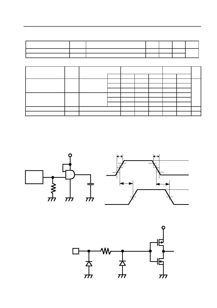
Miniaturized Logic IC Family
Rev.1.1
_00
S-75L08ANC
Seiko Instruments Inc.
39
AC Characteristics
C
L
=15pf, Input tr=tf=6ns, V
CC
=3.3
±0.3V, Ta=25
∞C (unless otherwise specified)
Parameter Sym.
Measurement
Conditions
MIN.
TYP.
MAX.
Unit
Output Rise/Fall Time
t
TLH,
t
THL
4.0 8.0 ns
Propagation Delay Time
t
pLH,
t
pHL
6.0 9.0
C
L
=25pf, Input tr=tf=6ns
(unless otherwise specified)
Parameter Sym.
Measurement
Conditions Ta=25
∞C
Ta=-40 to 85
∞C
Unit
V
CC
(V)
Min. Typ. Max. Min. Max.
t
TLH
1.0
35 70 90
Output Rise/Fall Time
t
THL
1.5
15 25 30
3.0
7 10 14
ns
t
pLH
1.0
30 60 75
Propagation Delay Time
t
pHL
1.5
15 25 30
3.0
7 10 14
Input Capacitance
C
IN
5 10 10
pF
Equiv. Int. Capacitance
C
PD
Note
1
10
pF
Note
1
C
PD
is the no-load equivalent capacitance inside the circuitry. Refer to the measurement circuit shown
below.
Current consumption is averaged by the following equation.
I
CC(
opr)
=C
PD
V
CC
fin+I
CC
Measurement Circuit
VIN
CL
50
VOUT
PG
tp
LH
50%
50%
10%
90%
tp
HL
6ns
VIN
VOUT
6ns
GND
VCC
VOL
VOH
50%
Remark No-load output during measurement of current consumption.
Input Pin Equivalent Circuit
Input pin
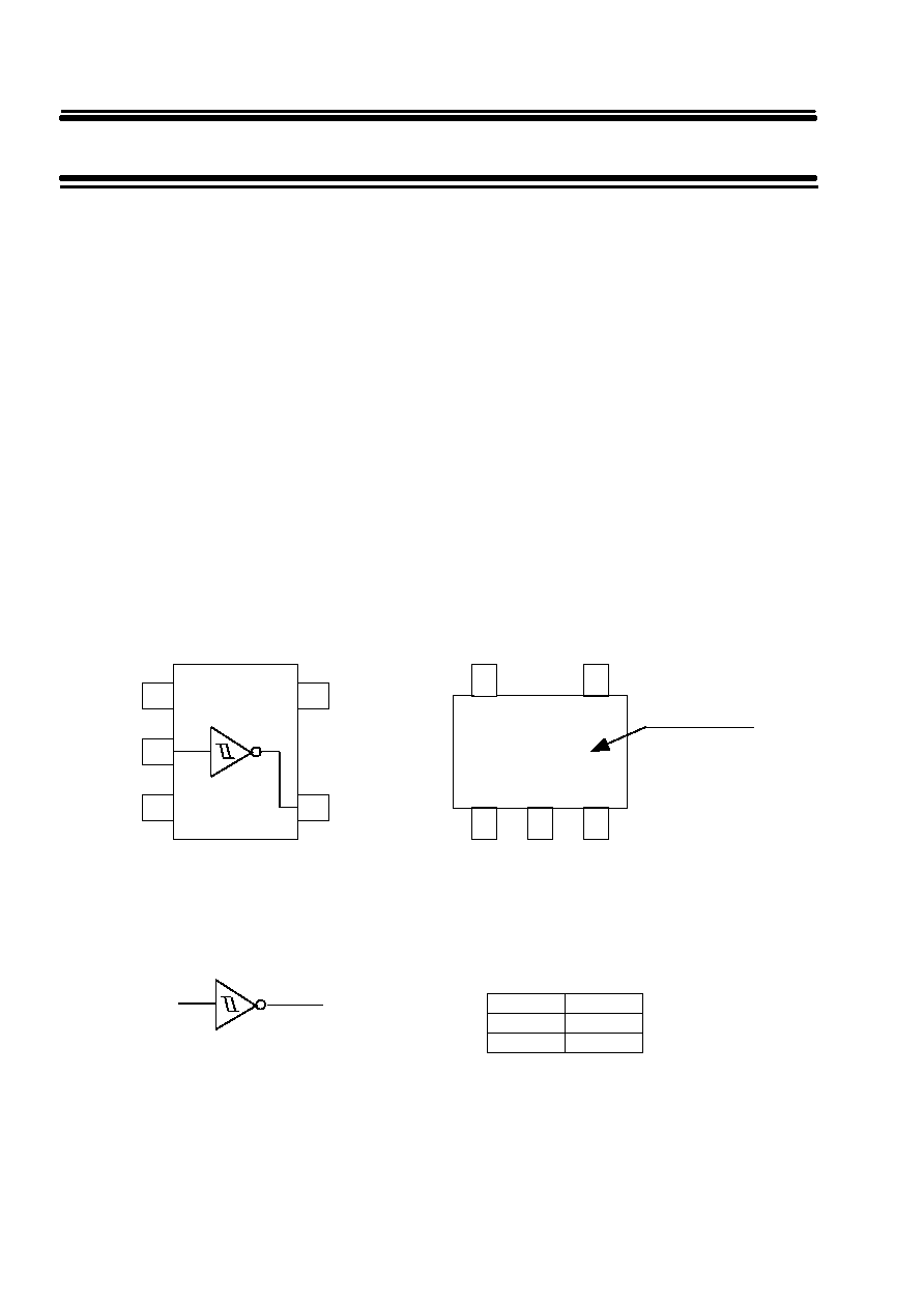
Rev.1.1
_00
40
Seiko Instruments Inc.
S-75L14ANC
SCHMITT INVERTER
The S-75L14ANC is a SCHMITT INVERTER fabricated by utilizing
advanced silicon-gate CMOS technology which provides the inherent
benefit of CMOS low power consumption to achieve operation by only a
couple of batteries (1 to 3V).
The internal circuitry has buffered outputs to ensure high noise immunity
and output stability.
Input voltage is allowed to be applied even if power voltage is not supplied
because no diode is inserted between an input pin and V
CC
.
This allows for interfaces between power supplies of different voltage,
output level conversion from 3 V to 1 V and battery backup applications.
Features
Applications
∑ Wide power supply range: 1 V to 3.6 V
∑ Personal computers, peripherals
∑ Low current consumption: 1.0 µA max. (at 3.6 V, 25∞C)
∑ Cellular phones
∑ Typical propagation delay: tpd = 8 ns (at 3 V)
∑ Cameras
∑ High noise immunity:
V
NIH
=V
NIL
=28% V
CC
min.
∑ Games
∑ Power down protection:
All pins
∑ Very small plastic package: SC-88A
Pin Assignment
Marking
Logic Diagram
True Values
A B
L H
H L
Model name
3
2
1
4
(Top view)
5
5LA
1
NC
IN A
GND
VCC
OUT Y
2
3
4
5
(Top view)
IN A
OUT Y
Miniaturized Logic IC Family
Rev.1.1
_00
S-75L14ANC
Seiko Instruments Inc.
41
Ordering
Delivery
form:
Taping
only
Model
name:
S-75L14ANC-5LA-TF
Absolute Maximum Ratings
Ta=25
∞C
Item Symbol
Ratings
Unit
Power Supply Voltage
V
CC
-0.5 to +5.0
V
Input Voltage
V
IN
-0.5 to +5.0
V
Output Voltage
V
OUT
-0.5 to V
CC
+0.5 V
Input Parasitic Diode Current
I
IK
-20 mA
Output Parasitic Diode Current
I
OK
±20 mA
Output Current
I
OUT
±12.5 mA
V
CC
/GND Current
I
CC
±25
mA
Power Dissipation
P
D
200
mW
Storage Temp. Range
Tstg
-65 to +150
∞C
Lead Temperature (10 sec.)
TL
260
∞C
Recommended Operating Conditions
Parameter
Symbol
Standard
Unit
Power Voltage
V
CC
1 to 3.6
V
Input Voltage
V
IN
0 to 3.6
V
Output Voltage
V
OUT
0 to V
CC
V
Op. Temp. Range
Topr
-40 to +85
∞C
0 to 1000 (V
CC
=1.0 V)
Input Rise and Fall Time
dt/dv
0 to 500 (V
CC
=2.0 V)
ns
0 to 400 (V
CC
=3.0 V)
DC Characteristics
Parameter
Sym.
Conditions Ta=25
∞C
Ta=-40 to 85
∞C
Unit
V
CC
MIN. TYP. MAX. MIN. MAX.
1.0
0.80
0.80
"H"
level
V
IH
1.5
1.20
1.20
Input
3.0
2.10
2.10 V
Voltage
1.0
0.20 0.20
"L"
level
V
IL
1.5
0.45 0.45
3.0
0.90 0.90
1.0
0.9
1.0
0.9
I
OH
=-20
µA 1.5 1.4 1.5
1.4
"H"
level
V
OH
V
IN
=V
IL
3.0 2.9 3.0
2.9
I
OH
=-1mA 1.5 1.07 1.23
0.99
Output I
OH
=-
2.6mA
3.0 2.61 2.68
2.55 V
Voltage
1.0
0 0.1 0.1
I
OL
=20
µA 1.5 0 0.1 0.1
"L"
level
V
OL
V
IN
=V
I
H
3.0
0 0.1 0.1
I
OL
=1mA 1.5
0.23 0.31 0.37
I
OL
=2.6mA 3.0
0.23 0.31 0.33
1.0
0.20
0.50
Hysteresis Voltage
V
H
1.5
0.25
0.50
V
3.0
0.45
0.65
Input Current
I
IN
V
IN
=V
CC
or GND
3.6
±0.1
±1.0
µA
Current Consump.
I
CC
V
IN
=V
CC
or GND
3.6
1.0 10.0
µA
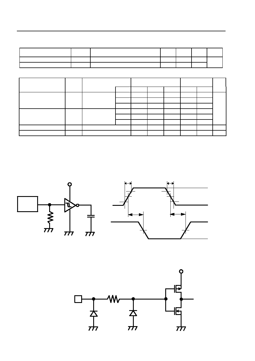
Miniaturized Logic IC Family
S-75L14ANC
Rev.1.1
_00
Seiko Instruments Inc.
42
AC Characteristics
C
L
=15pf, Input tr=tf=6ns, V
CC
=3.3
±0.3V, Ta=25
∞C (unless otherwise specified)
Parameter Sym.
Measurement
Conditions
MIN.
TYP.
MAX.
Unit
Output Rise/Fall Time
t
TLH,
t
THL
4.0 8.0
Propagation Delay Time
t
pLH,
t
pHL
4.0 10.5
C
L
=25pf, Input tr=tf=6ns
(unless otherwise specified)
Parameter Sym.
Measurement
Conditions Ta=25
∞C
Ta=-40 to 85
∞C
Unit
V
CC
(V)
Min. Typ. Max. Min. Max.
t
TLH
1.0
35 70 90
Output Rise/Fall Time
t
THL
1.5
15 25 30
3.0
7 10 14 ns
t
pLH
1.0
35 70 90
Propagation Delay Time
t
pHL
1.5
15 25 30
3.0
8 12 15
Input Capacitance
C
IN
5 10 10 pF
Equiv.Int. Capacitance
C
PD
Note
1
10
pF
Note
1
C
PD
is the no-load equivalent capacitance inside the circuitry. Refer to the measurement circuit shown
below.
Current consumption is averaged by the following equation.
I
CC(opr)
=C
PD
V
CC
fin+
I
CC
Measurement Circuit
VIN
CL
50
VOUT
PG.
tp
LH
50%
50%
10%
90%
tp
HL
6ns
VIN
VOUT
6ns
GND
VCC
VOL
VOH
50%
Remark No-load output during measurement of current consumption.
Input Pin Equivalent Circuit
Input pin
ns

Rev.1.1
_00
Seiko Instruments Inc.
43
S-75L32ANC
Single 2-Input OR Gate
The S-75L32ANC is a single
2-intput OR gate fabricated by utilizing
advanced silicon-gate CMOS technology which provides the inherent
benefit of CMOS low power consumption to achieve operation by only a
couple of batteries (1 to 3V).
The internal circuitry has buffered outputs to ensure high noise immunity
and output stability.
Input voltage is allowed to be applied even if power voltage is not supplied
because no diode is inserted between an input pin and V
CC
.
This allows for interfaces between power supplies of different voltage,
output level conversion from 3 V to 1 V and battery backup applications.
Features
Applications
∑ Wide power supply range: 1 V to 3.6 V
∑ Personal computers, peripherals
∑ Low current consumption: 1.0 µA max. (at 3.6 V, 25∞C)
∑ Cellular phones
∑ Typical propagation delay: tpd =7 ns (at 3 V)
∑ Cameras
∑ High noise immunity:
V
NIH
=V
NIL
=28% V
CC
min.
∑ Games
∑ Power down protection:
All pins
∑ Very small plastic package: SC-88A
Pin Assignment
Marking
Logic Diagram
True Values
A B Y
L L L
L H H
H L H
H H H
Model name
3
2
1
4
(Top view)
5
5L4
1
IN B
IN A
GND
VCC
OUT Y
2
3
4
5
(Top view)
IN B
IN A
OUT Y

Miniaturized Logic IC Family
S-75L32ANC
Rev.1.1
_00
Seiko Instruments Inc.
44
Ordering
Delivery
form:
Taping
only
Model
name:
S-75L32ANC-5L4-TF
Absolute Maximum Ratings
Ta=25
∞C
Item Symbol
Ratings
Unit
Power Supply Voltage
V
CC
-0.5 to +5.0
V
Input Voltage
V
IN
-0.5 to +5.0
V
Output Voltage
V
OUT
-0.5 to V
CC
+0.5 V
Input Parasitic Diode Current
I
IK
-20 mA
Output Parasitic Diode Current
I
OK
±20 mA
Output Current
I
OUT
±12.5 mA
V
CC
/GND Current
I
CC
±25
mA
Power Dissipation
P
D
200
mW
Storage Temp. Range
Tstg
-65 to +150
∞C
Lead Temperature (10 sec.)
TL
260
∞C
Recommended Operating Conditions
Parameter
Symbol
Standard
Unit
Power Voltage
V
CC
1 to 3.6
V
Input Voltage
V
IN
0 to 3.6
V
Output Voltage
V
OUT
0 to V
CC
V
Op. Temp. Range
Topr
-40 to +85
∞C
0 to 1000 (V
CC
=1.0 V)
Input Rise and Fall Time
dt/dv
0 to 500 (V
CC
=2.0 V)
ns
0 to 400 (V
CC
=3.0 V)
DC Characteristics
Parameter
Sym.
Conditions Ta=25
∞C
Ta=-40 to 85
∞C
Unit
V
CC
MIN. TYP. MAX. MIN. MAX.
1.0
0.75
0.75
"H"
level
V
IH
1.5
1.05
1.05
Input
3.0
2.10
2.10 V
Voltage
1.0
0.25 0.25
"L"
level
V
IL
1.5
0.45 0.45
3.0
0.90 0.90
1.0
0.9
1.0
0.9
V
IN
=V
I
H
I
OH
=-20
µA 1.5 1.4 1.5
1.4
"H"
level
V
OH
or
V
IL
3.0 2.9 3.0
2.9
I
OH
=-1mA 1.5 1.07 1.23
0.99
Output I
OH
=-
2.6mA
3.0 2.61 2.68
2.55 V
Voltage
1.0
0 0.1 0.1
I
OL
=20
µA 1.5 0 0.1 0.1
"L"
level
V
OL
V
IN
=V
IL
3.0
0 0.1 0.1
I
OL
=1mA 1.5
0.23 0.31 0.37
I
OL
=2.6mA 3.0
0.23 0.31 0.33
Input Current
I
IN
V
IN
=V
CC
or GND
3.6
±0.1
±1.0
µA
Current Consump.
I
CC
V
IN
=V
CC
or GND
3.6
1.0 10.0
µA

Miniaturized Logic IC Family
Rev.1.1
_00
S-75L32ANC
Seiko Instruments Inc.
45
AC Characteristics
C
L
=15pf, Input tr=tf=6ns, V
CC
=3.3
±0.3V, Ta=25
∞C (unless otherwise specified)
Parameter Sym.
Measurement
Conditions
MIN.
TYP.
MAX.
Unit
Output Rise/Fall Time
t
TLH,
t
THL
4.0 8.0 ns
Propagation Delay Time
t
pLH,
t
pHL
6.0 9.0
C
L
=25pf, Input tr=tf=6ns
(unless otherwise specified)
Parameter Sym.
Measurement
Conditions Ta=25
∞C
Ta=-40 to 85
∞C
Unit
V
CC
(V)
Min. Typ. Max. Min. Max.
t
TLH
1.0
35 70 90
Output Rise/Fall Time
t
THL
1.5
15 25 30
3.0
7 10 14
ns
t
pLH
1.0
30 60 75
Propagation Delay Time
t
pHL
1.5
15 25 30
3.0
7 10 14
Input Capacitance
C
IN
5 10 10
pF
Equiv. Int. Capacitance
C
PD
Note
1
10
pF
Note
1
C
PD
is the no-load equivalent capacitance inside the circuitry. Refer to the measurement circuit shown
below.
Current consumption is averaged by the following equation.
I
CC(opr)
=C
PD
V
CC
fin+I
CC
Measurement Circuit
VIN
CL
50
VOUT
PG
tp
LH
50%
50%
10%
90%
tp
HL
6ns
VIN
VOUT
6ns
GND
VCC
VOL
VOH
50%
Remark No-load output during measurement of current consumption.
Input Pin Equivalent Circuit
Input pin
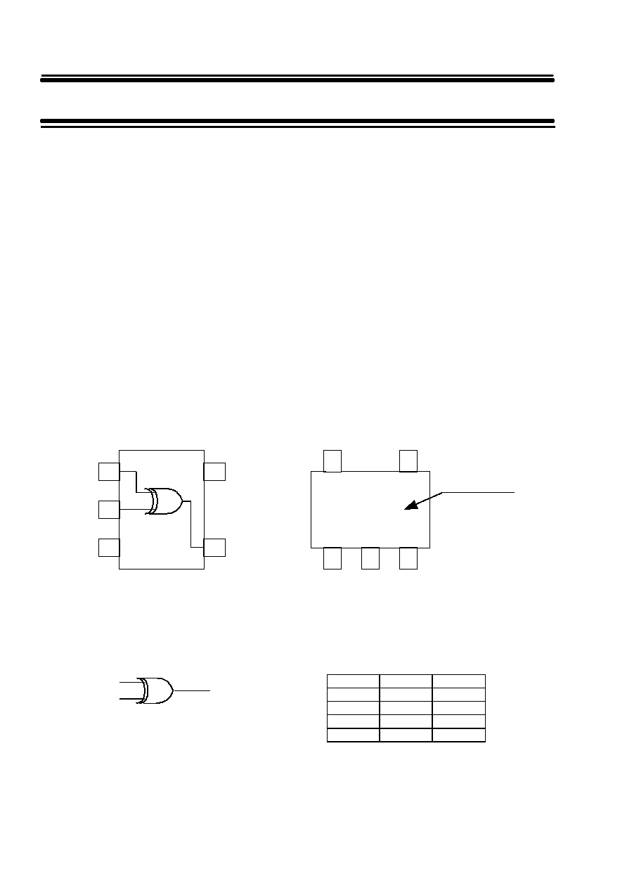
Rev.1.1
_00
46
Seiko Instruments Inc.
S-75L86ANC
EXCLUSIVE OR GATE
The S-75L86ANC is an EXCLUSIVE OR GATE fabricated by utilizing
advanced silicon-gate CMOS technology which provides the inherent
benefit of CMOS low power consumption to achieve operation by only a
couple of batteries (1 to 3V).
The internal circuitry has buffered outputs to ensure high noise immunity
and output stability.
Input voltage is allowed to be applied even if power voltage is not supplied
because no diode is inserted between an input pin and VCC.
This allows for interfaces between power supplies of different voltage,
output level conversion from 3 V to 1 V and battery backup applications.
Features
Applications
∑ Wide power supply range: 1 V to 3.6 V
∑ Personal computers, peripherals
∑ Low current consumption: 1.0 µA max. (at 3.6 V, 25∞C)
∑ Cellular phones
∑ Typical propagation delay: tpd = 7 ns (at 3 V)
∑ Cameras
∑ High noise immunity:
V
NIH
=V
NIL
=28% V
CC
min.
∑ Games
∑ Power down protection:
All pins
∑ Very small plastic package: SC-88A
Pin Assignment
Marking
Logic Diagram
True Values
A B Y
L L L
L H H
H L H
H H L
Model name
3
2
1
4
(Top view)
5
5L8
1
IN B
IN A
GND
VCC
OUT Y
2
3
4
5
(Top view)
IN B
IN A
OUT Y
Miniaturized Logic IC Family
Rev.1.1
_00
S-75L86ANC
Seiko Instruments Inc.
47
Ordering
Delivery
form:
Taping
only
Model
name:
S-75L86ANC-5L8-TF
Absolute Maximum Ratings
Ta=25
∞C
Item Symbol
Ratings
Unit
Power Supply Voltage
V
CC
-0.5 to +5.0
V
Input Voltage
V
IN
-0.5 to +5.0
V
Output Voltage
V
OUT
-0.5 to V
CC
+0.5 V
Input Parasitic Diode Current
I
IK
-20 mA
Output Parasitic Diode Current
I
OK
±20 mA
Output Current
I
OUT
±12.5 mA
V
CC
/GND Current
I
CC
±25
mA
Power Dissipation
P
D
200
mW
Storage Temp. Range
Tstg
-65 to +150
∞C
Lead Temperature (10 sec.)
TL
260
∞C
Recommended Operating Conditions
Parameter
Symbol
Standard
Unit
Power Voltage
V
CC
1 to 3.6
V
Input Voltage
V
IN
0 to 3.6
V
Output Voltage
V
OUT
0 to V
CC
V
Op. Temp. Range
Topr
-40 to +85
∞C
0 to 1000 (V
CC
=1.0 V)
Input Rise and Fall Time
dt/dv
0 to 500 (V
CC
=2.0 V)
ns
0 to 400 (V
CC
=3.0 V)
DC Characteristics
Parameter
Sym.
Conditions Ta=25
∞C
Ta=-40 to 85
∞C
Unit
V
CC
MIN. TYP. MAX. MIN. MAX.
1.0
0.75
0.75
"H"
level
V
IH
1.5
1.05
1.05
Input
3.0
2.10
2.10 V
Voltage
1.0
0.25 0.25
"L"
level
V
IL
1.5
0.45 0.45
3.0
0.90 0.90
1.0
0.9
1.0
0.9
V
IN
=V
I
H
I
OH
=-20
µA 1.5 1.4 1.5
1.4
"H"
level
V
OH
or
V
IL
3.0 2.9 3.0
2.9
I
OH
=-1mA 1.5 1.07 1.23
0.99
Output I
OH
=-
2.6mA
3.0 2.61 2.68
2.55 V
Voltage
1.0
0 0.1 0.1
V
IN
=V
I
H
I
OL
=20
µA 1.5 0 0.1 0.1
"L"
level
V
OL
or
V
IL
3.0
0 0.1 0.1
I
OL
=1mA 1.5
0.23 0.31 0.37
I
OL
=2.6mA 3.0
0.23 0.31 0.33
Input Current
I
IN
V
IN
=V
CC
or GND
3.6
±0.1
±1.0
µA
Current Consump.
I
CC
V
IN
=V
CC
or GND
3.6
1.0 10.0
µA
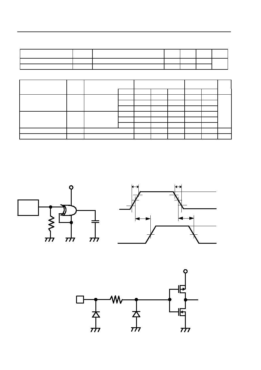
Miniaturized Logic IC Family
S-75L86ANC
Rev.1.1
_00
Seiko Instruments Inc.
48
AC Characteristics
C
L
=15pf, Input tr=tf=6ns, V
CC
=3.3
±0.3V, Ta=25
∞C (unless otherwise specified)
Parameter Sym.
Measurement
Conditions
MIN.
TYP.
MAX.
Unit
Output Rise/Fall Time
t
TLH,
t
THL
4.0 8.0 ns
Propagation Delay Time
t
pLH,
t
pHL
6.0 9.0
C
L
=25pf, Input tr=tf=6ns
(unless otherwise specified)
Parameter Sym.
Measurement
Conditions Ta=25
∞C
Ta=-40 to 85
∞C
Unit
V
CC
(V)
Min. Typ. Max. Min. Max.
t
TLH
1.0
35 70 90
Output Rise/Fall Time
t
THL
1.5
15 25 30
3.0
7 10 14 ns
t
pLH
1.0
30 60 75
Propagation Delay Time
t
pHL
1.5
15 25 30
3.0
7 10 14
Input Capacitance
C
IN
5 10 10 pF
Equiv. Int. Capacitance
C
PD
Note
1
10
pF
Note
1
C
PD
is the no-load equivalent capacitance inside the circuitry. Refer to the measurement circuit shown
below.
Current consumption is averaged by the following equation.
I
CC(opr)
=C
PD
V
CC
fin+I
CC
Measurement Circuit
VIN
CL
50
VOUT
PG
tp
LH
50%
50%
10%
90%
tp
HL
6ns
VIN
VOUT
6ns
GND
VCC
VOL
VOH
50%
Remark No-load output during measurement of current consumption.
Input Pin Equivalent Circuit
Input pin

2.0±0.2
1.3±0.1
0.15
+0.1
-0.05
0.65
0.65
1
2
3
4
5
n SC-88A
lDimensions
Unit mm
lTaping Specifications
lReel Specifications
No.:NP005-B-P-SD-1.0
NP005-B
Rev.1.1
020517
No. : NP005-B-C-SD-1.0
No. : NP005-B-R-SD-2.0
3000 pcs/reel
(2.25)
4.0±0.1 2.0±0.1
4.0±0.1
¯1.55±0.1
¯1.05±0.1
0.2±0.05
1.1±0.1
2.05±0.1
0.3
TF
1
2
3
4
5
Feed direction
12.5max.
9.0±0.3
¯13±0.2
(60∞) (60∞)
Winding core
0.2
+0.1
-0.05

∑
The information described herein is subject to change without notice.
∑
Seiko Instruments Inc. is not responsible for any problems caused by circuits or diagrams described herein
whose related industrial properties, patents, or other rights belong to third parties. The application circuit
examples explain typical applications of the products, and do not guarantee the success of any specific
mass-production design.
∑
When the products described herein are regulated products subject to the Wassenaar Arrangement or other
agreements, they may not be exported without authorization from the appropriate governmental authority.
∑
Use of the information described herein for other purposes and/or reproduction or copying without the
express permission of Seiko Instruments Inc. is strictly prohibited.
∑
The products described herein cannot be used as part of any device or equipment affecting the human
body, such as exercise equipment, medical equipment, security systems, gas equipment, or any apparatus
installed in airplanes and other vehicles, without prior written permission of Seiko Instruments Inc.
∑
Although Seiko Instruments Inc. exerts the greatest possible effort to ensure high quality and reliability, the
failure or malfunction of semiconductor products may occur. The user of these products should therefore
give thorough consideration to safety design, including redundancy, fire-prevention measures, and
malfunction prevention, to prevent any accidents, fires, or community damage that may ensue.