Document Outline
- S-808xxC Series
- Cover
- Features
- Applications
- Packages
- Block Diagrams
- Product Name Structure
- Output Forms
- Pin Configurations
- Absolute Maximum Ratings
- Electrical Characteristics
- Test Circuits
- Timing Chart
- Operation
- Standard Circuit
- Technical Terms
- Electrical Characteristics for Customized Products
- Precautions
- Typical Characteristics (Typical Data)
- Package Drawings
- SC-82AB
- SOT-23-5
- SOT-89-3
- SNT-4A
- TO-92(Bulk)
- TO-92 Tape and Reel)
- YF003-A(Package)
- YF003-A(Tape)
- YF003-A(Reel)
- TO-92(Tape and Ammo)
- YF003-A(Package)
- YZ003-C(Tape)
- YZ003-C(Zigzag)

Rev.3.2
_00
ULTRA-SMALL PACKAGE HIGH-PRECISION
VOLTAGE DETECTOR
S-808xxC Series
Seiko Instruments Inc.
1
The S-808xxC series is a series of high-precision
voltage detectors developed using CMOS process. The
detection voltage is fixed internally with an accuracy of
±2.0%. Two output forms, Nch open-drain and CMOS
output, are available. Ultra-low current consumption
and miniature package lineup can meet demand from
the portable device applications.
Features
∑ Ultra-low current consumption
1.3
µA typ. (detection voltage1.4 V, at V
DD
=1.5 V)
0.8
µA typ. (detection voltage1.5 V, at V
DD
=3.5 V)
∑ High-precision detection voltage ±2.0 %
∑ Operating voltage range
0.65 V to 5.0 V (detection voltage
1.4 V)
0.95 V to 10.0 V (detection voltage
1.5 V)
∑ Hysteresis characteristics
5 % typ.
∑ Detection voltage
0.8 V to 6.0 V (0.1 V step)
∑ Output form
Nch open-drain output (Active Low)
CMOS output (Active Low)
Applications
∑ Battery checkers
∑ Power failure detectors
∑ Power monitor for portable equipments such as pagers, calculators, electronic notebooks and remote
controllers.
∑ Constant voltage power monitor for cameras, video equipments and communication devices.
∑ Power monitor for microcomputers and reset for CPUs.
Packages
Package name
Drawing code
Package
Tape
Reel
Zigzag
SC-82AB
NP004-A NP004-A NP004-A
SOT-23-5
MP005-A MP005-A MP005-A
SOT-89-3
UP003-A UP003-A UP003-A
SNT-4A
PF004-A PF004-A PF004-A
TO-92 (Bulk)
YS003-B
TO-92 (Tape and reel)
YF003-A
YF003-A
YF003-A
TO-92 (Tape and ammo)
YF003-A
YZ003-C
YZ003-C

ULTRA-SMALL PACKAGE HIGH-PRECISION VOLTAGE DETECTOR
S-808xxC Series
Rev.3.2
_00
2
Seiko Instruments Inc.
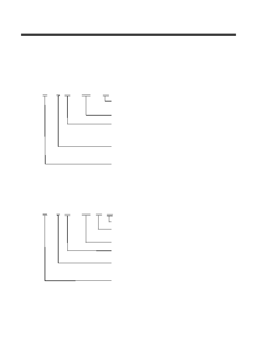
Block Diagrams
1. Nch Open-drain Output Products
VSS
*1
*1
+
-
OUT
VDD
V
REF
*1. Parasitic diode
Figure 1
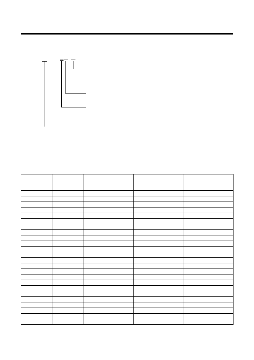
2. CMOS Output Products
*1
-
+
OUT
VSS
VDD
*1
*1
V
REF
*1. Parasitic diode
Figure 2
ULTRA-SMALL PACKAGE HIGH-PRECISION VOLTAGE DETECTOR
Rev.3.2
_00
S-808xxC Series
Seiko Instruments Inc.
3
Product Name Structure
The detection voltage, output form and packages for S-808xxC Series can be selected at the user's request.
Refer to the "1. Product Name" for the construction of the product name and "2. Product Name List" for the
full product names.
1. Product Name
1-1. SC-82AB, SOT-23-5, SOT-89-3 packages
S-808xx C x xx
- xxx - T2
IC detection in tape specifications
*1
T2: SC-82AB, SOT-23-5, SOT-89-3
Product code
*2
Package code
NB: SC-82AB
MC: SOT-23-5
UA: SOT-89-3
Output form
N: Nch open-drain output (Active Low)
L: CMOS output (Active Low)
Detection voltage value
08 to 60
(e.g. When the detection voltage is 0.8 V,
it is expressed as 08.)
*1. Refer to the taping specifications at the end of this book. T2 is the standard.
*2. Refer to the Table 1 and 3 in the "2. Product Name List"
1-2. SNT-4A packages
S-808xx C x PF
- xxx TF G
Fixed
IC detection in tape specifications
*1
TF: SNT-4A
Product code
*2
Package code
PF: SNT-4A
Output form
N: Nch open-drain output (Active Low)
L: CMOS output (Active Low)
Detection voltage value
08 to 60
(e.g. When the detection voltage is 0.8 V,
it is expressed as 08.)
*1. Refer to the taping specifications at the end of this book. TF is the standard.
*2. Refer to the Table 2 and 4 in the "2. Product Name List"
ULTRA-SMALL PACKAGE HIGH-PRECISION VOLTAGE DETECTOR
S-808xxC Series
Rev.3.2
_00
4
Seiko Instruments Inc.
1-3. TO-92 package
S-808xx C x Y - x
Packing form
B: Bulk
T: Tape and reel
Z: Tape and ammo
Package code
Y: TO-92
Output form
N: Nch open-drain output (Active Low)
L: CMOS output (Active Low)
Detection voltage value
15 to 60
(e.g. When the detection voltage is 1.5 V,
it is expressed as 15.)
2. Product Name List
2-1. Nch Open-drain Output Products
Table 1 (1/2)
Detection
voltage range
Hysteresis width
(Typ.)
SC-82AB SOT-23-5 SOT-89-3
0.8 V
±2.0 %
0.034 V
S-80808CNNB-B9M-T2
0.9 V
±2.0 %
0.044 V
S-80809CNNB-B9N-T2
1.0 V
±2.0 %
0.054 V
S-80810CNNB-B9O-T2
1.1 V
±2.0 %
0.064 V
S-80811CNNB-B9P-T2
1.2 V
±2.0 %
0.073 V
S-80812CNNB-B9Q-T2
1.3 V
±2.0 %
0.083 V
S-80813CNNB-B9R-T2
1.4 V
±2.0 %
0.093 V
S-80814CNNB-B9S-T2
1.5 V
±2.0 %
0.075 V
S-80815CNNB-B8A-T2
S-80815CNMC-B8A-T2 S-80815CNUA-B8A-T2
1.6 V
±2.0 %
0.080 V
S-80816CNNB-B8B-T2
S-80816CNMC-B8B-T2 S-80816CNUA-B8B-T2
1.7 V
±2.0 %
0.085 V
S-80817CNNB-B8C-T2
S-80817CNMC-B8C-T2
S-80817CNUA-B8C-T2
1.8 V
±2.0 %
0.090 V
S-80818CNNB-B8D-T2
S-80818CNMC-B8D-T2
S-80818CNUA-B8D-T2
1.9 V
±2.0 %
0.095 V
S-80819CNNB-B8E-T2
S-80819CNMC-B8E-T2 S-80819CNUA-B8E-T2
2.0 V
±2.0 %
0.100 V
S-80820CNNB-B8F-T2
S-80820CNMC-B8F-T2 S-80820CNUA-B8F-T2
2.1 V
±2.0 %
0.105 V
S-80821CNNB-B8G-T2
S-80821CNMC-B8G-T2 S-80821CNUA-B8G-T2
2.2 V
±2.0 %
0.110 V
S-80822CNNB-B8H-T2
S-80822CNMC-B8H-T2
S-80822CNUA-B8H-T2
2.3 V
±2.0 %
0.115 V
S-80823CNNB-B8I-T2
S-80823CNMC-B8I-T2 S-80823CNUA-B8I-T2
2.4 V
±2.0 %
0.120 V
S-80824CNNB-B8J-T2
S-80824CNMC-B8J-T2 S-80824CNUA-B8J-T2
2.4 V typ.
4.4
± 0.1 V
*1
S-80824KNUA-D2B-T2
*2
2.5 V
±2.0 %
0.125 V
S-80825CNNB-B8K-T2
S-80825CNMC-B8K-T2 S-80825CNUA-B8K-T2
2.6 V
±2.0 %
0.130 V
S-80826CNNB-B8L-T2
S-80826CNMC-B8L-T2 S-80826CNUA-B8L-T2
2.7 V
±2.0 %
0.135 V
S-80827CNNB-B8M-T2
S-80827CNMC-B8M-T2 S-80827CNUA-B8M-T2
2.8 V
±2.0 %
0.140 V
S-80828CNNB-B8N-T2
S-80828CNMC-B8N-T2
S-80828CNUA-B8N-T2
2.9 V
±2.0 %
0.145 V
S-80829CNNB-B8O-T2
S-80829CNMC-B8O-T2 S-80829CNUA-B8O-T2
3.0 V
±2.0 %
0.150 V
S-80830CNNB-B8P-T2
S-80830CNMC-B8P-T2 S-80830CNUA-B8P-T2
3.1 V
±2.0 %
0.155 V
S-80831CNNB-B8Q-T2
S-80831CNMC-B8Q-T2 S-80831CNUA-B8Q-T2

ULTRA-SMALL PACKAGE HIGH-PRECISION VOLTAGE DETECTOR
Rev.3.2
_00
S-808xxC Series
Seiko Instruments Inc.
5
Table 1 (2/2)
Detection
voltage range
Hysteresis width
(Typ.)
SC-82AB SOT-23-5 SOT-89-3
3.2 V
±2.0 %
0.160 V
S-80832CNNB-B8R-T2
S-80832CNMC-B8R-T2
S-80832CNUA-B8R-T2
3.3 V
±2.0 %
0.165 V
S-80833CNNB-B8S-T2
S-80833CNMC-B8S-T2 S-80833CNUA-B8S-T2
3.4 V
±2.0 %
0.170 V
S-80834CNNB-B8T-T2
S-80834CNMC-B8T-T2 S-80834CNUA-B8T-T2
3.5 V
±2.0 %
0.175 V
S-80835CNNB-B8U-T2
S-80835CNMC-B8U-T2
S-80835CNUA-B8U-T2
3.6 V
±2.0 %
0.180 V
S-80836CNNB-B8V-T2
S-80836CNMC-B8V-T2 S-80836CNUA-B8V-T2
3.7 V
±2.0 %
0.185 V
S-80837CNNB-B8W-T2
S-80837CNMC-B8W-T2 S-80837CNUA-B8W-T2
3.8 V
±2.0 %
0.190 V
S-80838CNNB-B8X-T2
S-80838CNMC-B8X-T2 S-80838CNUA-B8X-T2
3.9 V
±2.0 %
0.195 V
S-80839CNNB-B8Y-T2
S-80839CNMC-B8Y-T2 S-80839CNUA-B8Y-T2
4.0 V
±2.0 %
0.200 V
S-80840CNNB-B8Z-T2
S-80840CNMC-B8Z-T2 S-80840CNUA-B8Z-T2
4.1 V
±2.0 %
0.205 V
S-80841CNNB-B82-T2
S-80841CNMC-B82-T2 S-80841CNUA-B82-T2
4.2 V
±2.0 %
0.210 V
S-80842CNNB-B83-T2
S-80842CNMC-B83-T2 S-80842CNUA-B83-T2
4.3 V
±2.0 %
0.215 V
S-80843CNNB-B84-T2
S-80843CNMC-B84-T2 S-80843CNUA-B84-T2
4.4 V
±2.0 %
0.220 V
S-80844CNNB-B85-T2
S-80844CNMC-B85-T2 S-80844CNUA-B85-T2
4.5 V
±2.0 %
0.225 V
S-80845CNNB-B86-T2
S-80845CNMC-B86-T2 S-80845CNUA-B86-T2
4.6 V
±2.0 %
0.230 V
S-80846CNNB-B87-T2
S-80846CNMC-B87-T2 S-80846CNUA-B87-T2
4.6 V
± 0.10 V
0.10 V max.
S-80846KNUA-D2C-T2*
3
4.7 V
±2.0 %
0.235 V
S-80847CNNB-B88-T2
S-80847CNMC-B88-T2 S-80847CNUA-B88-T2
4.8 V
±2.0 %
0.240 V
S-80848CNNB-B89-T2
S-80848CNMC-B89-T2 S-80848CNUA-B89-T2
4.9 V
±2.0 %
0.245 V
S-80849CNNB-B9A-T2
S-80849CNMC-B9A-T2 S-80849CNUA-B9A-T2
5.0 V
±2.0 %
0.250 V
S-80850CNNB-B9B-T2
S-80850CNMC-B9B-T2 S-80850CNUA-B9B-T2
5.1 V
±2.0 %
0.255 V
S-80851CNNB-B9C-T2
S-80851CNMC-B9C-T2
S-80851CNUA-B9C-T2
5.2 V
±2.0 %
0.260 V
S-80852CNNB-B9D-T2
S-80852CNMC-B9D-T2
S-80852CNUA-B9D-T2
5.3 V
±2.0 %
0.265 V
S-80853CNNB-B9E-T2
S-80853CNMC-B9E-T2 S-80853CNUA-B9E-T2
5.4 V
±2.0 %
0.270 V
S-80854CNNB-B9F-T2
S-80854CNMC-B9F-T2 S-80854CNUA-B9F-T2
5.5 V
±2.0 %
0.275 V
S-80855CNNB-B9G-T2
S-80855CNMC-B9G-T2 S-80855CNUA-B9G-T2
5.6 V
±2.0 %
0.280 V
S-80856CNNB-B9H-T2
S-80856CNMC-B9H-T2
S-80856CNUA-B9H-T2
5.7 V
±2.0 %
0.285 V
S-80857CNNB-B9I-T2
S-80857CNMC-B9I-T2 S-80857CNUA-B9I-T2
5.8 V
±2.0 %
0.290 V
S-80858CNNB-B9J-T2
S-80858CNMC-B9J-T2 S-80858CNUA-B9J-T2
5.9 V
±2.0 %
0.295 V
S-80859CNNB-B9K-T2
S-80859CNMC-B9K-T2 S-80859CNUA-B9K-T2
6.0 V
±2.0 %
0.300 V
S-80860CNNB-B9L-T2
S-80860CNMC-B9L-T2 S-80860CNUA-B9L-T2
*1. Describes the release voltage.
*2. Refer to the Table 18 in " Electricala Characteristics for Customized Products" for electrical characteristics.
*3. Refer to the Table 20 in " Electricala Characteristics for Customized Products" for electrical characteristics

ULTRA-SMALL PACKAGE HIGH-PRECISION VOLTAGE DETECTOR
S-808xxC Series
Rev.3.2
_00
6
Seiko Instruments Inc.
Table 2 (1/2)
Detection
voltage range
Hysteresis width
(Typ.)
SNT-4A TO-92
*1
0.8 V
±2.0 %
0.034 V
S-80808CNPF-B9MTFG
0.9 V
±2.0 %
0.044 V
S-80809CNPF-B9NTFG
1.0 V
±2.0 %
0.054 V
S-80810CNPF-B9OTFG
1.1 V
±2.0 %
0.064 V
S-80811CNPF-B9PTFG
1.2 V
±2.0 %
0.073 V
S-80812CNPF-B9QTFG
1.3 V
±2.0 %
0.083 V
S-80813CNPF-B9RTFG
1.4 V
±2.0 %
0.093 V
S-80814CNPF-B9STFG
1.5 V
±2.0 %
0.075 V
S-80815CNPF-B8ATFG
S-80815CNY-x
1.6 V
±2.0 %
0.080 V
S-80816CNPF-B8BTFG
S-80816CNY-x
1.7 V
±2.0 %
0.085 V
S-80817CNPF-B8CTFG
S-80817CNY-x
1.8 V
±2.0 %
0.090 V
S-80818CNPF-B8DTFG
S-80818CNY-x
1.9 V
±2.0 %
0.095 V
S-80819CNPF-B8ETFG
S-80819CNY-x
2.0 V
±2.0 %
0.100 V
S-80820CNPF-B8FTFG
S-80820CNY-x
2.1 V
±2.0 %
0.105 V
S-80821CNPF-B8GTFG
S-80821CNY-x
2.2 V
±2.0 %
0.110 V
S-80822CNPF-B8HTFG
S-80822CNY-x
2.3 V
±2.0 %
0.115 V
S-80823CNPF-B8ITFG
S-80823CNY-x
2.4 V
±2.0 %
0.120 V
S-80824CNPF-B8JTFG
S-80824CNY-x
2.4 V typ.
4.4
± 0.1 V
*2
S-80824KNY-x
*3
2.5 V
±2.0 %
0.125 V
S-80825CNPF-B8KTFG
S-80825CNY-x
2.6 V
±2.0 %
0.130 V
S-80826CNPF-B8LTFG
S-80826CNY-x
2.7 V
±2.0 %
0.135 V
S-80827CNPF-B8MTFG
S-80827CNY-x
2.8 V
±2.0 %
0.140 V
S-80828CNPF-B8NTFG
S-80828CNY-x
2.9 V
±2.0 %
0.145 V
S-80829CNPF-B8OTFG
S-80829CNY-x
3.0 V
±2.0 %
0.150 V
S-80830CNPF-B8PTFG
S-80830CNY-x
3.1 V
±2.0 %
0.155 V
S-80831CNPF-B8QTFG
S-80831CNY-x
3.2 V
±2.0 %
0.160 V
S-80832CNPF-B8RTFG
S-80832CNY-x
3.3 V
±2.0 %
0.165 V
S-80833CNPF-B8STFG
S-80833CNY-x
3.4 V
±2.0 %
0.170 V
S-80834CNPF-B8TTFG
S-80834CNY-x
3.5 V
±2.0 %
0.175 V
S-80835CNPF-B8UTFG
S-80835CNY-x
3.6 V
±2.0 %
0.180 V
S-80836CNPF-B8VTFG
S-80836CNY-x
3.7 V
±2.0 %
0.185 V
S-80837CNPF-B8WTFG
S-80837CNY-x
3.8 V
±2.0 %
0.190 V
S-80838CNPF-B8XTFG
S-80838CNY-x
3.9 V
±2.0 %
0.195 V
S-80839CNPF-B8YTFG
S-80839CNY-x
4.0 V
±2.0 %
0.200 V
S-80840CNPF-B8ZTFG
S-80840CNY-x
4.1 V
±2.0 %
0.205 V
S-80841CNPF-B82TFG
S-80841CNY-x
4.2 V
±2.0 %
0.210 V
S-80842CNPF-B83TFG
S-80842CNY-x
4.3 V
±2.0 %
0.215 V
S-80843CNPF-B84TFG
S-80843CNY-x
4.4 V
±2.0 %
0.220 V
S-80844CNPF-B85TFG
S-80844CNY-x
4.5 V
±2.0 %
0.225 V
S-80845CNPF-B86TFG
S-80845CNY-x
4.6 V
±2.0 %
0.230 V
S-80846CNPF-B87TFG
S-80846CNY-x
4.6 V
±0.10 V
0.10 V max.
S-80846KNY-x
*4
4.7 V
±2.0 %
0.235 V
S-80847CNPF-B88TFG
S-80847CNY-x
4.8 V
±2.0 %
0.240 V
S-80848CNPF-B89TFG
S-80848CNY-x
4.9 V
±2.0 %
0.245 V
S-80849CNPF-B9ATFG
S-80849CNY-x
5.0 V
±2.0 %
0.250 V
S-80850CNPF-B9BTFG
S-80850CNY-x
5.1 V
±2.0 %
0.255 V
S-80851CNPF-B9CTFG
S-80851CNY-x

ULTRA-SMALL PACKAGE HIGH-PRECISION VOLTAGE DETECTOR
Rev.3.2
_00
S-808xxC Series
Seiko Instruments Inc.
7
Table 2 (2/2)
Detection
voltage range
Hysteresis width
(Typ.)
SNT-4A TO-92
*1
5.2 V
±2.0 %
0.260 V
S-80852CNPF-B9DTFG
S-80852CNY-x
5.3 V
±2.0 %
0.265 V
S-80853CNPF-B9ETFG
S-80853CNY-x
5.4 V
±2.0 %
0.270 V
S-80854CNPF-B9FTFG
S-80854CNY-x
5.5 V
±2.0 %
0.275 V
S-80855CNPF-B9GTFG
S-80855CNY-x
5.6 V
±2.0 %
0.280 V
S-80856CNPF-B9HTFG
S-80856CNY-x
5.7 V
±2.0 %
0.285 V
S-80857CNPF-B9ITFG
S-80857CNY-x
5.8 V
±2.0 %
0.290 V
S-80858CNPF-B9JTFG
S-80858CNY-x
5.9 V
±2.0 %
0.295 V
S-80859CNPF-B9KTFG
S-80859CNY-x
6.0 V
±2.0 %
0.300 V
S-80860CNPF-B9LTFG
S-80860CNY-x
*1. x changes according to the packing form in TO-92. S: Bulk, F: Tape and reel, Z: Tape and ammo
*2. Describes the release voltage.
*3. Refer to the Table 18 in " Electricala Characteristics for Customized Products" for electrical characteristics.
*4. Refer to the Table 20 in " Electricala Characteristics for Customized Products" for electrical characteristics

ULTRA-SMALL PACKAGE HIGH-PRECISION VOLTAGE DETECTOR
S-808xxC Series
Rev.3.2
_00
8
Seiko Instruments Inc.
2-2. CMOS Output Products
Table 3 (1/2)
Detection
voltage range
Hysteresis width
(Typ.)
SC-82AB SOT-23-5 SOT-89-3
0.8 V
±2.0 %
0.034 V
S-80808CLNB-B7M-T2
0.9 V
±2.0 %
0.044 V
S-80809CLNB-B7N-T2
1.0 V
±2.0 %
0.054 V
S-80810CLNB-B7O-T2
1.1 V
±2.0 %
0.064 V
S-80811CLNB-B7P-T2
1.2 V
±2.0 %
0.073 V
S-80812CLNB-B7Q-T2
1.3 V
±2.0 %
0.083 V
S-80813CLNB-B7R-T2
1.4 V
±2.0 %
0.093 V
S-80814CLNB-B7S-T2
1.5 V
±2.0 %
0.075 V
S-80815CLNB-B6A-T2
S-80815CLMC-B6A-T2
S-80815CLUA-B6A-T2
1.6 V
±2.0 %
0.080 V
S-80816CLNB-B6B-T2
S-80816CLMC-B6B-T2
S-80816CLUA-B6B-T2
1.7 V
±2.0 %
0.085 V
S-80817CLNB-B6C-T2
S-80817CLMC-B6C-T2
S-80817CLUA-B6C-T2
1.8 V
±2.0 %
0.090 V
S-80818CLNB-B6D-T2
S-80818CLMC-B6D-T2
S-80818CLUA-B6D-T2
1.9 V
±2.0 %
0.095 V
S-80819CLNB-B6E-T2
S-80819CLMC-B6E-T2
S-80819CLUA-B6E-T2
2.0 V
±2.0 %
0.100 V
S-80820CLNB-B6F-T2
S-80820CLMC-B6F-T2 S-80820CLUA-B6F-T2
2.1 V
±2.0 %
0.105 V
S-80821CLNB-B6G-T2
S-80821CLMC-B6G-T2 S-80821CLUA-B6G-T2
2.2 V
±2.0 %
0.110 V
S-80822CLNB-B6H-T2
S-80822CLMC-B6H-T2
S-80822CLUA-B6H-T2
2.3 V
±2.0 %
0.115 V
S-80823CLNB-B6I-T2
S-80823CLMC-B6I-T2
S-80823CLUA-B6I-T2
2.4 V
±2.0 %
0.120 V
S-80824CLNB-B6J-T2
S-80824CLMC-B6J-T2
S-80824CLUA-B6J-T2
2.5 V
±2.0 %
0.125 V
S-80825CLNB-B6K-T2
S-80825CLMC-B6K-T2
S-80825CLUA-B6K-T2
2.6 V
±2.0 %
0.130 V
S-80826CLNB-B6L-T2
S-80826CLMC-B6L-T2 S-80826CLUA-B6L-T2
2.7 V
±2.0 %
0.135 V
S-80827CLNB-B6M-T2
S-80827CLMC-B6M-T2
S-80827CLUA-B6M-T2
2.8 V
±2.0 %
0.140 V
S-80828CLNB-B6N-T2
S-80828CLMC-B6N-T2
S-80828CLUA-B6N-T2
2.9 V
±2.0 %
0.145 V
S-80829CLNB-B6O-T2
S-80829CLMC-B6O-T2 S-80829CLUA-B6O-T2
3.0 V
±2.0 %
0.150 V
S-80830CLNB-B6P-T2
S-80830CLMC-B6P-T2
S-80830CLUA-B6P-T2
3.1 V
±2.0 %
0.155 V
S-80831CLNB-B6Q-T2
S-80831CLMC-B6Q-T2 S-80831CLUA-B6Q-T2
3.2 V
±2.0 %
0.160 V
S-80832CLNB-B6R-T2
S-80832CLMC-B6R-T2
S-80832CLUA-B6R-T2
3.3 V
±2.0 %
0.165 V
S-80833CLNB-B6S-T2
S-80833CLMC-B6S-T2
S-80833CLUA-B6S-T2
3.4 V
±2.0 %
0.170 V
S-80834CLNB-B6T-T2
S-80834CLMC-B6T-T2 S-80834CLUA-B6T-T2
3.5 V
±2.0 %
0.175 V
S-80835CLNB-B6U-T2
S-80835CLMC-B6U-T2
S-80835CLUA-B6U-T2
3.6 V
±2.0 %
0.180 V
S-80836CLNB-B6V-T2
S-80836CLMC-B6V-T2
S-80836CLUA-B6V-T2
3.7 V
±2.0 %
0.185 V
S-80837CLNB-B6W-T2
S-80837CLMC-B6W-T2
S-80837CLUA-B6W-T2
3.8 V
±2.0 %
0.190 V
S-80838CLNB-B6X-T2
S-80838CLMC-B6X-T2
S-80838CLUA-B6X-T2
3.9 V
±2.0 %
0.195 V
S-80839CLNB-B6Y-T2
S-80839CLMC-B6Y-T2
S-80839CLUA-B6Y-T2
4.0 V
±2.0 %
0.200 V
S-80840CLNB-B6Z-T2
S-80840CLMC-B6Z-T2 S-80840CLUA-B6Z-T2
4.1 V
±2.0 %
0.205 V
S-80841CLNB-B62-T2
S-80841CLMC-B62-T2 S-80841CLUA-B62-T2
4.2 V
±2.0 %
0.210 V
S-80842CLNB-B63-T2
S-80842CLMC-B63-T2 S-80842CLUA-B63-T2
4.3 V
±2.0 %
0.215 V
S-80843CLNB-B64-T2
S-80843CLMC-B64-T2 S-80843CLUA-B64-T2
4.4 V
±2.0 %
0.220 V
S-80844CLNB-B65-T2
S-80844CLMC-B65-T2 S-80844CLUA-B65-T2
4.45 V typ.
4.70 V max.
*1
S-80844KLUA-D2A-T2*
2
4.5 V
±2.0 %
0.225 V
S-80845CLNB-B66-T2
S-80845CLMC-B66-T2 S-80845CLUA-B66-T2
4.6 V
±2.0 %
0.230 V
S-80846CLNB-B67-T2
S-80846CLMC-B67-T2 S-80846CLUA-B67-T2
4.7 V
±2.0 %
0.235 V
S-80847CLNB-B68-T2
S-80847CLMC-B68-T2 S-80847CLUA-B68-T2
4.8 V
±2.0 %
0.240 V
S-80848CLNB-B69-T2
S-80848CLMC-B69-T2 S-80848CLUA-B69-T2
4.9 V
±2.0 %
0.245 V
S-80849CLNB-B7A-T2
S-80849CLMC-B7A-T2
S-80849CLUA-B7A-T2
5.0 V
±2.0 %
0.250 V
S-80850CLNB-B7B-T2
S-80850CLMC-B7B-T2
S-80850CLUA-B7B-T2
5.1 V
±2.0 %
0.255 V
S-80851CLNB-B7C-T2
S-80851CLMC-B7C-T2
S-80851CLUA-B7C-T2
ULTRA-SMALL PACKAGE HIGH-PRECISION VOLTAGE DETECTOR
Rev.3.2
_00
S-808xxC Series
Seiko Instruments Inc.
9
Table 3 (2/2)
Detection
voltage range
Hysteresis width
(Typ.)
SC-82AB SOT-23-5 SOT-89-3
5.2 V
±2.0 %
0.260 V
S-80852CLNB-B7D-T2
S-80852CLMC-B7D-T2
S-80852CLUA-B7D-T2
5.3 V
±2.0 %
0.265 V
S-80853CLNB-B7E-T2
S-80853CLMC-B7E-T2
S-80853CLUA-B7E-T2
5.4 V
±2.0 %
0.270 V
S-80854CLNB-B7F-T2
S-80854CLMC-B7F-T2 S-80854CLUA-B7F-T2
5.5 V
±2.0 %
0.275 V
S-80855CLNB-B7G-T2
S-80855CLMC-B7G-T2 S-80855CLUA-B7G-T2
5.6 V
±2.0 %
0.280 V
S-80856CLNB-B7H-T2
S-80856CLMC-B7H-T2
S-80856CLUA-B7H-T2
5.7 V
±2.0 %
0.285 V
S-80857CLNB-B7I-T2
S-80857CLMC-B7I-T2
S-80857CLUA-B7I-T2
5.8 V
±2.0 %
0.290 V
S-80858CLNB-B7J-T2
S-80858CLMC-B7J-T2
S-80858CLUA-B7J-T2
5.9 V
±2.0 %
0.295 V
S-80859CLNB-B7K-T2
S-80859CLMC-B7K-T2
S-80859CLUA-B7K-T2
6.0 V
±2.0 %
0.300 V
S-80860CLNB-B7L-T2
S-80860CLMC-B7L-T2 S-80860CLUA-B7L-T2
*1. Describes the release voltage.
*2. Refer to the Table 19 in " Electricala Characteristics for Customized Products" for electrical characteristics.
Table 4 (1/2)
Detection
voltage range
Hysteresis width
(Typ.)
SNT-4A TO-92
*1
0.8 V
±2.0 %
0.034 V
S-80808CLPF-B7MTFG
0.9 V
±2.0 %
0.044 V
S-80809CLPF-B7NTFG
1.0 V
±2.0 %
0.054 V
S-80810CLPF-B7OTFG
1.1 V
±2.0 %
0.064 V
S-80811CLPF-B7PTFG
1.2 V
±2.0 %
0.073 V
S-80812CLPF-B7QTFG
1.3 V
±2.0 %
0.083 V
S-80813CLPF-B7RTFG
1.4 V
±2.0 %
0.093 V
S-80814CLPF-B7STFG
1.5 V
±2.0 %
0.075 V
S-80815CLPF-B6ATFG
S-80815CLY-x
1.6 V
±2.0 %
0.080 V
S-80816CLPF-B6BTFG
S-80816CLY-x
1.7 V
±2.0 %
0.085 V
S-80817CLPF-B6CTFG
S-80817CLY-x
1.8 V
±2.0 %
0.090 V
S-80818CLPF-B6DTFG
S-80818CLY-x
1.9 V
±2.0 %
0.095 V
S-80819CLPF-B6ETFG
S-80819CLY-x
2.0 V
±2.0 %
0.100 V
S-80820CLPF-B6FTFG
S-80820CLY-x
2.1 V
±2.0 %
0.105 V
S-80821CLPF-B6GTFG
S-80821CLY-x
2.2 V
±2.0 %
0.110 V
S-80822CLPF-B6HTFG
S-80822CLY-x
2.3 V
±2.0 %
0.115 V
S-80823CLPF-B6ITFG
S-80823CLY-x
2.4 V
±2.0 %
0.120 V
S-80824CLPF-B6JTFG
S-80824CLY-x
2.5 V
±2.0 %
0.125 V
S-80825CLPF-B6KTFG
S-80825CLY-x
2.6 V
±2.0 %
0.130 V
S-80826CLPF-B6LTFG
S-80826CLY-x
2.7 V
±2.0 %
0.135 V
S-80827CLPF-B6MTFG
S-80827CLY-x
2.8 V
±2.0 %
0.140 V
S-80828CLPF-B6NTFG
S-80828CLY-x
2.9 V
±2.0 %
0.145 V
S-80829CLPF-B6OTFG
S-80829CLY-x
3.0 V
±2.0 %
0.150 V
S-80830CLPF-B6PTFG
S-80830CLY-x
3.1 V
±2.0 %
0.155 V
S-80831CLPF-B6QTFG
S-80831CLY-x
3.2 V
±2.0 %
0.160 V
S-80832CLPF-B6RTFG
S-80832CLY-x
3.3 V
±2.0 %
0.165 V
S-80833CLPF-B6STFG
S-80833CLY-x
3.4 V
±2.0 %
0.170 V
S-80834CLPF-B6TTFG
S-80834CLY-x
3.5 V
±2.0 %
0.175 V
S-80835CLPF-B6UTFG
S-80835CLY-x
3.6 V
±2.0 %
0.180 V
S-80836CLPF-B6VTFG
S-80836CLY-x
3.7 V
±2.0 %
0.185 V
S-80837CLPF-B6WTFG
S-80837CLY-x
3.8 V
±2.0 %
0.190 V
S-80838CLPF-B6XTFG
S-80838CLY-x

ULTRA-SMALL PACKAGE HIGH-PRECISION VOLTAGE DETECTOR
S-808xxC Series
Rev.3.2
_00
10
Seiko Instruments Inc.
Table 4 (2/2)
Detection
voltage range
Hysteresis width
(Typ.)
SNT-4A TO-92
*2
3.9 V
±2.0 %
0.195 V
S-80839CLPF-B6YTFG
S-80839CLY-x
4.0 V
±2.0 %
0.200 V
S-80840CLPF-B6ZTFG
S-80840CLY-x
4.1 V
±2.0 %
0.205 V
S-80841CLPF-B62TFG
S-80841CLY-x
4.2 V
±2.0 %
0.210 V
S-80842CLPF-B63TFG
S-80842CLY-x
4.3 V
±2.0 %
0.215 V
S-80843CLPF-B64TFG
S-80843CLY-x
4.4 V
±2.0 %
0.220 V
S-80844CLPF-B65TFG
S-80844CLY-x
4.45 V typ.
4.70 V max.
*2
S-80844KLY-x
*3
4.5 V
±2.0 %
0.225 V
S-80845CLPF-B66TFG
S-80845CLY-x
4.6 V
±2.0 %
0.230 V
S-80846CLPF-B67TFG
S-80846CLY-x
4.7 V
±2.0 %
0.235 V
S-80847CLPF-B68TFG
S-80847CLY-x
4.8 V
±2.0 %
0.240 V
S-80848CLPF-B69TFG
S-80848CLY-x
4.9 V
±2.0 %
0.245 V
S-80849CLPF-B7ATFG
S-80849CLY-x
5.0 V
±2.0 %
0.250 V
S-80850CLPF-B7BTFG
S-80850CLY-x
5.1 V
±2.0 %
0.255 V
S-80851CLPF-B7CTFG
S-80851CLY-x
5.2 V
±2.0 %
0.260 V
S-80852CLPF-B7DTFG
S-80852CLY-x
5.3 V
±2.0 %
0.265 V
S-80853CLPF-B7ETFG
S-80853CLY-x
5.4 V
±2.0 %
0.270 V
S-80854CLPF-B7FTFG
S-80854CLY-x
5.5 V
±2.0 %
0.275 V
S-80855CLPF-B7GTFG
S-80855CLY-x
5.6 V
±2.0 %
0.280 V
S-80856CLPF-B7HTFG
S-80856CLY-x
5.7 V
±2.0 %
0.285 V
S-80857CLPF-B7ITFG
S-80857CLY-x
5.8 V
±2.0 %
0.290 V
S-80858CLPF-B7JTFG
S-80858CLY-x
5.9 V
±2.0 %
0.295 V
S-80859CLPF-B7KTFG
S-80859CLY-x
6.0 V
±2.0 %
0.300 V
S-80860CLPF-B7LTFG
S-80860CLY-x
*1. x changes according to the packing form in TO-92. S: Bulk, F: Tape and reel, Z: Tape and ammo
*2. Describes the release voltage.
*3. Refer to the Table 19 in " Electricala Characteristics for Customized Products" for electrical characteristics.
ULTRA-SMALL PACKAGE HIGH-PRECISION VOLTAGE DETECTOR
Rev.3.2
_00
S-808xxC Series
Seiko Instruments Inc.
11
Output Forms
1. Output Forms in S-808xxC Series
Table 5
Nch open-drain output products
(Active Low)
CMOS output products
(Active Low)
S-808xxC Series
"N" is the last letter of the product name.
e.g. S-80815CN
"L" is the last letter of the product name.
e.g. S-80815CL
2. Output form and their usage
Table 6
Usage
Nch open-drain output products
(Active Low)
CMOS output products
(Active Low)
Different power supplies
Yes
No
Active Low reset for CPUs
Yes
Yes
Active High reset for CPUs
No
No
Detection voltage change by resistor divider
Yes
No
∑ Example for two power supplies ∑ Example for one power supply
V/D
Nch
V/D
Nch
V/D
CMOS
CPU
CPU
CPU
V
DD1
V
DD2
V
DD
V
DD
OUT OUT
OUT
V
SS
V
SS
V
SS
Figure 3

ULTRA-SMALL PACKAGE HIGH-PRECISION VOLTAGE DETECTOR
S-808xxC Series
Rev.3.2
_00
12
Seiko Instruments Inc.
Pin Configurations
Table 7
Pin No.
Pin name
Pin description
1
OUT
Voltage detection output pin
2
VDD
Voltage input pin
3 NC
*1
No connection
4 VSS
GND
pin
4 3
1
2
SC-82AB
Top view
*1.
The NC pin is electrically open.
The NC pin can be connected to VDD or VSS.
Figure 4
Table 8
Pin No.
Pin name
Pin description
1
OUT
Voltage detection output pin
2
VDD
Voltage input pin
3 VSS
GND
pin
4 NC
*1
No connection
5 NC
*1
No connection
SOT-23-5
Top view
5
4
3
2
1
*1.
The NC pin is electrically open.
The NC pin can be connected to VDD or VSS.
Figure 5
Table 9
Pin No.
Pin name
Pin description
1
OUT
Voltage detection output pin
2
VDD
Voltage input pin
3 VSS
GND
pin
SOT-89-3
Top view
3
2
1
Figure 6
Table10
Pin No.
Pin name
Pin description
1
OUT
Voltage detection output pin
2 VSS
GND
pin
3 NC
*1
No connection
4
VDD
Voltage input pin
SNT-4A
Top view
1
4
2 3
*1.
The NC pin is electrically open.
The NC pin can be connected to VDD or VSS.
Figure 7
ULTRA-SMALL PACKAGE HIGH-PRECISION VOLTAGE DETECTOR
Rev.3.2
_00
S-808xxC Series
Seiko Instruments Inc.
13
Table 11
Pin No.
Pin name
Pin description
1
OUT
Voltage detection output pin
2
VDD
Voltage input pin
3 VSS
GND
pin
TO-92
Bottom view
1
3
2
Figure 8
Absolute Maximum Ratings
1. Detection Voltage Typ. 1.4 V or Less Products
Table 12
(Ta
=25∞C unless otherwise specified
Item
Symbol
Absolute maximum ratings Unit
Power supply voltage
V
DD
-V
SS
7 V
Output voltage Nch open-drain output products
V
OUT
V
SS
-0.3 to V
SS
+7
CMOS output products
V
SS
-0.3 to V
DD
+0.3
Output current
I
OUT
50
mA
Power dissipation
P
D
SC-82AB
150
mW
SNT-4A
140
Operating ambient temperature
Topr
-40 to +85
∞C
Storage temperature
Tstg
-40 to +125
Caution The absolute maximum ratings are rated values exceeding which the product could suffer
physical damage. These values must therefore not be exceeded under any conditions.
2. Detection Voltage Typ. 1.5 V or More Products
Table 13
(Ta
=25∞C unless otherwise specified
Item
Symbol
Absolute maximum ratings Unit
Power supply voltage
V
DD
-V
SS
12 V
Output voltage Nch open-drain output products
V
OUT
V
SS
-0.3 to V
SS
+12
CMOS output products
V
SS
-0.3 to V
DD
+0.3
Output current
I
OUT
50
mA
Power dissipation
P
D
SC-82AB
150
mW
SOT-23-5
250
SOT-89-3
500
SNT-4A
140
TO-92
400
Operating ambient temperature
Topr
-40 to +85
∞C
Storage temperature
Tstg
-40 to +125
Caution The absolute maximum ratings are rated values exceeding which the product could suffer
physical damage. These values must therefore not be exceeded under any conditions.
ULTRA-SMALL PACKAGE HIGH-PRECISION VOLTAGE DETECTOR
S-808xxC Series
Rev.3.2
_00
14
Seiko Instruments Inc.
Electrical Characteristics
1. Nch Open-drain Output Products
1-1. Detection Voltage Typ.1.4 V or Less Products
Table 14
(Ta
=25∞C unless otherwise specified)
Item Symbol Condition Min.
Typ.
Max.
Unit
Test
circuit
Detection voltage
*1
-V
DET
-V
DET(S)
◊0.98
-V
DET(S)
-V
DET(S)
◊1.02
V 1
Release voltage
+V
DET
S-80808 0.802 0.834 0.867
S-80809 0.910 0.944 0.979
S-80810 1.017 1.054 1.091
S-80811 1.125 1.164 1.203
S-80812 1.232 1.273 1.315
S-80813 1.340 1.383 1.427
S-80814 1.448 1.493 1.538
Hysteresis width
V
HYS
S-80808 0.018 0.034 0.051
S-80809 0.028 0.044 0.061
S-80810 0.037 0.054 0.071
S-80811 0.047 0.064 0.081
S-80812 0.056 0.073 0.091
S-80813 0.066 0.083 0.101
S-80814 0.076 0.093 0.110
Current consumption
I
SS
V
DD
=1.5 V
S-80808 to 09
1.3 3.5
µA
2
V
DD
=2.0 V
S-80810 to 14
1.3 3.5
Operating voltage
V
DD
0.65
5.0 V 1
Output current
I
OUT
Output transistor,
Nch, V
DS
=0.5 V, V
DD
=0.7 V
0.04 0.2
mA 3
Leakage current
I
LEAK
Output transistor,
Nch, V
DS
=5.0 V, V
DD
=5.0 V
60 nA
Response time
t
PLH
60
µs
1
Detection voltage
temperature
coefficient
*2
DET
DET
V
Ta
V
-
∑
-
Ta
=-40 ∞C to +85 ∞C
±100
±350 ppm/∞C
*1.
-V
DET
: Actual detection voltage value,
-V
DET(S)
: Specified detection voltage value (The center value of the
detection voltage range in Table 1 to 2.)
*2.
The temperature change ratio in the detection voltage [mV/∞C] is calculated by using the following equation.
[
]
(
)
[ ]
[
]
1000
C
ppm/
V
Ta
V
V
Typ.
V
C
mV/
Ta
V
DET
DET
DET(S)
DET
˜
∞
-
-
◊
-
=
∞
-
∑
3
*
2
*
*1
*1.
Temperature change ratio of the detection voltage
*2.
Specified detection voltage
*3.
Detection voltage temperature coefficient
ULTRA-SMALL PACKAGE HIGH-PRECISION VOLTAGE DETECTOR
Rev.3.2
_00
S-808xxC Series
Seiko Instruments Inc.
15
1-2. Detection Voltage Typ.1.5 V or More Products
Table 15
(Ta
=25∞C unless otherwise specified)
Item Symbol
Condition Min.
Typ.
Max.
Unit
Test
circuit
Detection voltage
*1
-V
DET
-V
DET(S)
◊0.98
-V
DET(S)
-V
DET(S)
◊1.02
V 1
Hysteresis width
V
HYS
-V
DET
◊0.03
-V
DET
◊0.05
-V
DET
◊0.08
Current consumption
I
SS
V
DD
=3.5 V
S-80815 to 26
0.8 2.4
µA
2
V
DD
=4.5 V
S-80827 to 39
0.8 2.4
V
DD
=6.0 V
S-80840 to 56
0.9 2.7
V
DD
=7.5 V
S-80857 to 60
0.9 2.7
Operating voltage
V
DD
0.95
10.0 V 1
Output current
I
OUT
Output transistor,
Nch, V
DS
=0.5 V
V
DD
=1.2 V
S-80815 to 60
0.59 1.36
mA
3
V
DD
=2.4 V
S-80827 to 60
2.88 4.98
Leakage current
I
LEAK
Output transistor,
Nch, V
DS
=10.0 V, V
DD
=10.0 V
100 nA
Response time
t
PLH
60
µs
1
Detection voltage
temperature
coefficient
*2
DET
DET
V
Ta
V
-
∑
-
Ta
=-40 ∞C to +85 ∞C
±100
±350
ppm/
∞C
*1.
-V
DET
: Actual detection voltage value,
-V
DET(S)
: Specified detection voltage value (The center value of the
detection voltage range in Table 1 to 2.)
*2.
The temperature change ratio in the detection voltage [mV/∞C] is calculated by using the following equation.
[
]
(
)
[ ]
[
]
1000
C
ppm/
V
Ta
V
V
Typ.
V
C
mV/
Ta
V
DET
DET
DET(S)
DET
˜
∞
-
-
◊
-
=
∞
-
∑
3
*
2
*
*1
*1.
Temperature change ratio of the detection voltage
*2.
Specified detection voltage
*3.
Detection voltage temperature coefficient
ULTRA-SMALL PACKAGE HIGH-PRECISION VOLTAGE DETECTOR
S-808xxC Series
Rev.3.2
_00
16
Seiko Instruments Inc.
2. CMOS Output Products
2-1. Detection Voltage Typ.1.4 V or Less Products
Table 16
(Ta
=25∞C unless otherwise specified)
Item Symbol Condition Min.
Typ.
Max.
Unit
Test
circuit
Detection voltage
*1
-V
DET
-V
DET(S)
◊0.98
-V
DET(S)
-V
DET(S)
◊1.02
V 1
Release voltage
+V
DET
S-80808 0.802 0.834 0.867
S-80809 0.910 0.944 0.979
S-80810 1.017 1.054 1.091
S-80811 1.125 1.164 1.203
S-80812 1.232 1.273 1.315
S-80813 1.340 1.383 1.427
S-80814 1.448 1.493 1.538
Hysteresis width
V
HYS
S-80808 0.018 0.034 0.051
S-80809 0.028 0.044 0.061
S-80810 0.037 0.054 0.071
S-80811 0.047 0.064 0.081
S-80812 0.056 0.073 0.091
S-80813 0.066 0.083 0.101
S-80814 0.076 0.093 0.110
Current consumption
I
SS
V
DD
=1.5 V
S-80808 to 09
1.3 3.5
µA
2
V
DD
=2.0 V
S-80810 to 14
1.3 3.5
Operating voltage
V
DD
0.65
5.0 V 1
Output current
I
OUT
Output transistor,
Nch, V
DS
=0.5 V, V
DD
=0.7 V
0.04 0.2
mA 3
Output transistor,
Pch, V
DS
=2.1 V, V
DD
=4.5 V
2.9 5.8
4
Response time
t
PLH
60
µs
1
Detection voltage
temperature
coefficient
*2
DET
DET
V
Ta
V
-
∑
-
Ta
=-40 ∞C to +85 ∞C
±100
±350 ppm/∞C
*1.
-V
DET
: Actual detection voltage value,
-V
DET(S)
: Specified detection voltage value (The center value of the
detection voltage range in Table 3 to 4.)
*2.
The temperature change ratio in the detection voltage [mV/∞C] is calculated by using the following equation.
[
]
(
)
[ ]
[
]
1000
C
ppm/
V
Ta
V
V
Typ.
V
C
mV/
Ta
V
DET
DET
DET(S)
DET
˜
∞
-
-
◊
-
=
∞
-
∑
3
*
2
*
*1
*1.
Temperature change ratio of the detection voltage
*2.
Specified detection voltage
*3.
Detection voltage temperature coefficient
ULTRA-SMALL PACKAGE HIGH-PRECISION VOLTAGE DETECTOR
Rev.3.2
_00
S-808xxC Series
Seiko Instruments Inc.
17
2-2.
Detection Voltage Typ.1.5 V or More Products
Table 17
(Ta
=25∞C unless otherwise specified)
Item Symbol
Condition Min.
Typ.
Max.
Unit
Test
circuit
Detection voltage
*1
-V
DET
-V
DET(S)
◊0.98
-V
DET(S)
-V
DET(S)
◊1.02
V 1
Hysteresis width
V
HYS
-V
DET
◊0.03
-V
DET
◊0.05
-V
DET
◊0.08
Current consumption
I
SS
V
DD
=3.5 V
S-80815 to 26
0.8 2.4
µA
2
V
DD
=4.5 V
S-80827 to 39
0.8 2.4
V
DD
=6.0 V
S-80840 to 56
0.9 2.7
V
DD
=7.5 V
S-80857 to 60
0.9 2.7
Operating voltage
V
DD
0.95
10.0 V 1
Output current
I
OUT
Output
transistor,
Nch, V
DS
=0.5 V
V
DD
=1.2 V
S-80815 to 60
0.59 1.36
mA
3
V
DD
=2.4 V
S-80827 to 60
2.88 4.98
Output transistor,
Pch, V
DS
=0.5 V
V
DD
=4.8 V
S-80815 to 39
1.43 2.39
4
V
DD
=6.0 V
S-80840 to 56
1.68 2.78
V
DD
=8.4 V
S-80857 to 60
2.08 3.42
Response time
t
PLH
60
µs
1
Detection voltage
temperature
coefficient
*2
DET
DET
V
Ta
V
-
∑
-
Ta
=-40 ∞C to +85 ∞C
±100
±350
ppm/
∞C
*1.
-V
DET
: Actual detection voltage value,
-V
DET(S)
: Specified detection voltage value (The center value of the
detection voltage range in Table 3 to 4.)
*2.
The temperature change ratio in the detection voltage [mV/∞C] is calculated by using the following equation.
[
]
(
)
[ ]
[
]
1000
C
ppm/
V
Ta
V
V
Typ.
V
C
mV/
Ta
V
DET
DET
DET(S)
DET
˜
∞
-
-
◊
-
=
∞
-
∑
3
*
2
*
*1
*1.
Temperature change ratio of the detection voltage
*2.
Specified detection voltage
*3.
Detection voltage temperature coefficient

ULTRA-SMALL PACKAGE HIGH-PRECISION VOLTAGE DETECTOR
S-808xxC Series
Rev.3.2
_00
18
Seiko Instruments Inc.
Test Circuits
1.
S-808xxC
Series
V
V
DD
VDD
VSS
OUT
V
R
*1
100 k
*1.
R is unnecessary for CMOS output products.
Figure 9
2.
S-808xxC
Series
A
V
DD
VDD
VSS
OUT
Figure 10
3.
S-808xxC
Series
V
V
DS
V
DD
VDD
VSS
OUT
V
A
Figure 11
4.
S-808xxC
Series
V
V
DD
V
DS
VDD
VSS
OUT
V
A
Figure 12
ULTRA-SMALL PACKAGE HIGH-PRECISION VOLTAGE DETECTOR
Rev.3.2
_00
S-808xxC Series
Seiko Instruments Inc.
19
Timing Chart
1. Nch Open-drain Output Products
V
OUT
VDD
VSS
R
100 k
Release voltage (
+V
DET
)
Detection voltage (
-V
DET
)
V
D D
V
SS
Minimum operating voltage
Output from the OUT pin
Hysteresis width (V
HYS
)
V
DD
V
SS
Figure 13
2. CMOS Output Products
V
OUT
VDD
VSS
Release voltage (
+V
DET
)
Detection voltage (
-V
DET
)
V
DD
V
SS
Minimum operating voltage
Hysteresis width (V
HYS
)
Output from the OUT pin
V
SS
V
DD
Remark
For values of V
DD
less than minimum operating voltage, values of OUT terminal output is free in the
shaded region.
Figure 14

ULTRA-SMALL PACKAGE HIGH-PRECISION VOLTAGE DETECTOR
S-808xxC Series
Rev.3.2
_00
20
Seiko Instruments Inc.
Operation
1. Basic Operation: CMOS Output (Active Low)
1-1.
When the power supply voltage (V
DD
) is higher than the release voltage (
+V
DET
), the Nch transistor is
OFF and the Pch transistor is ON to provide V
DD
(high) at the output. Since the Nch transistor N1 in
Figure 15
is OFF, the comparator input voltage is
C
B
A
DD
C
B
R
R
R
V
)
R
R
(
+
+
∑
+
.
1-2.
When the V
DD
goes below
+V
DET
, the output provides the V
DD
level, as long as the V
DD
remains above
the detection voltage
-V
DET
. When the V
DD
falls below
-V
DET
(point A in Figure 16), the Nch transistor
becomes ON, the Pch transistor becomes OFF, and the V
SS
level appears at the output. At this time
the Nch transistor N1 in Figure 15 becomes ON, the comparator input voltage is changed to
B
A
DD
B
R
R
V
R
+
∑
.
1-3.
When the V
DD
falls below the minimum operating voltage, the output becomes undefined, or goes to the
V
DD
when the output is pulled up to the V
DD
.
1-4.
The V
SS
level appears when the V
DD
rises above the minimum operating voltage. The V
SS
level still
appears even when the V
DD
surpasses
-V
DET
, as long as it does not exceed the release voltage
+V
DET
.
1-5.
When the V
DD
rises above
+V
DET
(point B in Figure 16), the Nch transistor becomes OFF and the Pch
transistor becomes ON to provide V
DD
level at the output.
V
REF
Pch
Nch
N1
R
C
R
B
R
A
-
+
OUT
VSS
VDD
*1
*1
*1
*1.
Parasiteic diode
Figure 15 Operation 1
ULTRA-SMALL PACKAGE HIGH-PRECISION VOLTAGE DETECTOR
Rev.3.2
_00
S-808xxC Series
Seiko Instruments Inc.
21
Hysteresis width (V
HYS
)
A
B
V
DD
V
SS
Minimum operating voltage
Output from the OUT pin
V
DD
V
SS
(1)
(2)
(3)
(5)
(4)
Release voltage (
+V
DET
)
Detection voltage (
-V
DET
)
Figure 16 Operation 2
2.
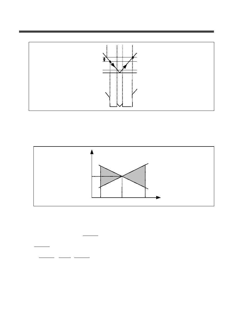
Other Characteristics
2-1. Temperature Characteristics of Detection Voltage
The shaded area in Figure 17 shows the temperature characteristics of the detection voltage.
-40 25
+0.945 mV/∞C
-V
DET
[V]
85 Ta
[∞C]
-0.945 mV/∞C
-V
DET25
*1
*1.
-V
DET25
is an actual detection voltage value at 25∞C.
Figure 17 Temperature Characteristics of Detection Voltage (Example for S-80827C)
2-2. Temperature Characteristics of Release Voltage
The temperature coefficient
Ta
V
DET
+
for the release voltage is calculated by the temperature coefficient
Ta
V
DET
-
of the detection voltage as follows:
Ta
V
V
V
Ta
V
DET
DET
DET
DET
-
◊
-
+
=
+
The temperature coefficients for the release voltage and the detection voltage have the same sign
consequently.
ULTRA-SMALL PACKAGE HIGH-PRECISION VOLTAGE DETECTOR
S-808xxC Series
Rev.3.2
_00
22
Seiko Instruments Inc.
2-3. Temperature Characteristics of Hysteresis Voltage
The temperature characteristics for the hysteresis voltage is expressed as
Ta
V
Ta
V
DET
DET
-
-
+
and is
calculated as follows:
Ta
V
V
V
Ta
V
Ta
V
DET
DET
HYS
DET
DET
-
◊
-
=
-
-
+
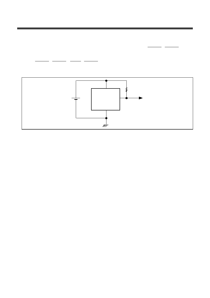
Standard Circuit
VDD
OUT
VSS
R*
1
100 k
*1.
R is unnecessary for CMOS output products.
Figure 18
Caution The above connection diagram and constants do not guarantee correct operation. Perform
sufficient evaluation using the actual application to set the constants.
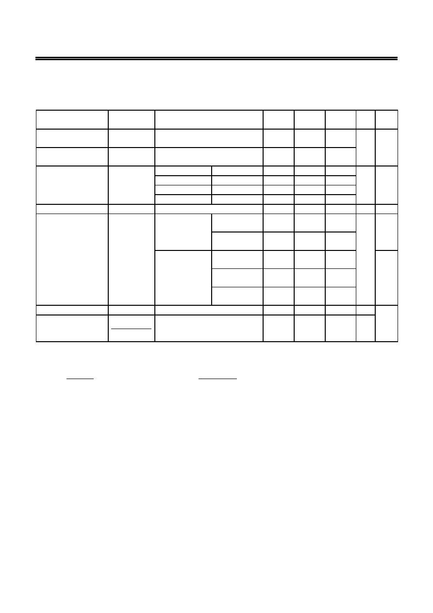
Technical Terms
1. Detection Voltage (
-V
DET
), Release Voltage (
+V
DET
)
The detection voltage (
-V
DET
) is a voltage at which the output turns to low. The detection voltage varies slightly
among products of the same specification. The variation of detection voltage between the specified minimum
(
-V
DET
) Min. and the maximum (
-V
DET
) Max. is called the detection voltage range (Refer to Figure 19).
Example: For the S-80815CN, the detection voltage lies in the range of 1.470
(-V
DET
)
1.530.
This means that some S-80815CNs have 1.470 V for
-V
DET
and some have 1.530 V.
The release voltage (
+V
DET
) is a voltage at which the output turns to high. The release voltage varies slightly
among products of the same specification. The variation of release voltages between the specified
minimum (
+V
DET
) Min. and the maximum (
+V
DET
) Max. is called the release voltage range (Refer to Figure
20
). The range is calculed from the actual detection voltage (
-V
DET
)
of a product and is expressed by
-V
DET
◊1.03+V
DET
-V
DET
◊1.08.
Example: For the S-80815CN, the release voltage lies in the range of 1.514
(+V
DET
)
1.652.
This means that some S-80815CNs have 1.514 V for
+V
DET
and some have 1.652 V.
ULTRA-SMALL PACKAGE HIGH-PRECISION VOLTAGE DETECTOR
Rev.3.2
_00
S-808xxC Series
Seiko Instruments Inc.
23
V
DD
OUT
(
-V
DET
) Max.
(
-V
DET
) Min.
Detection voltage range
Detection voltage
(
+V
DET
) Max.
(
+V
DET
) Min.
Release voltage range
V
DD
Release voltage
OUT
Figure 19 Detection Voltage (CMOS Output Products) Figure 20 Release Voltage (CMOS Output Products)
Remark
Although the detection voltage and release voltage overlap in the range of 1.514 V to 1.530 V,
+V
DET
is always larger than
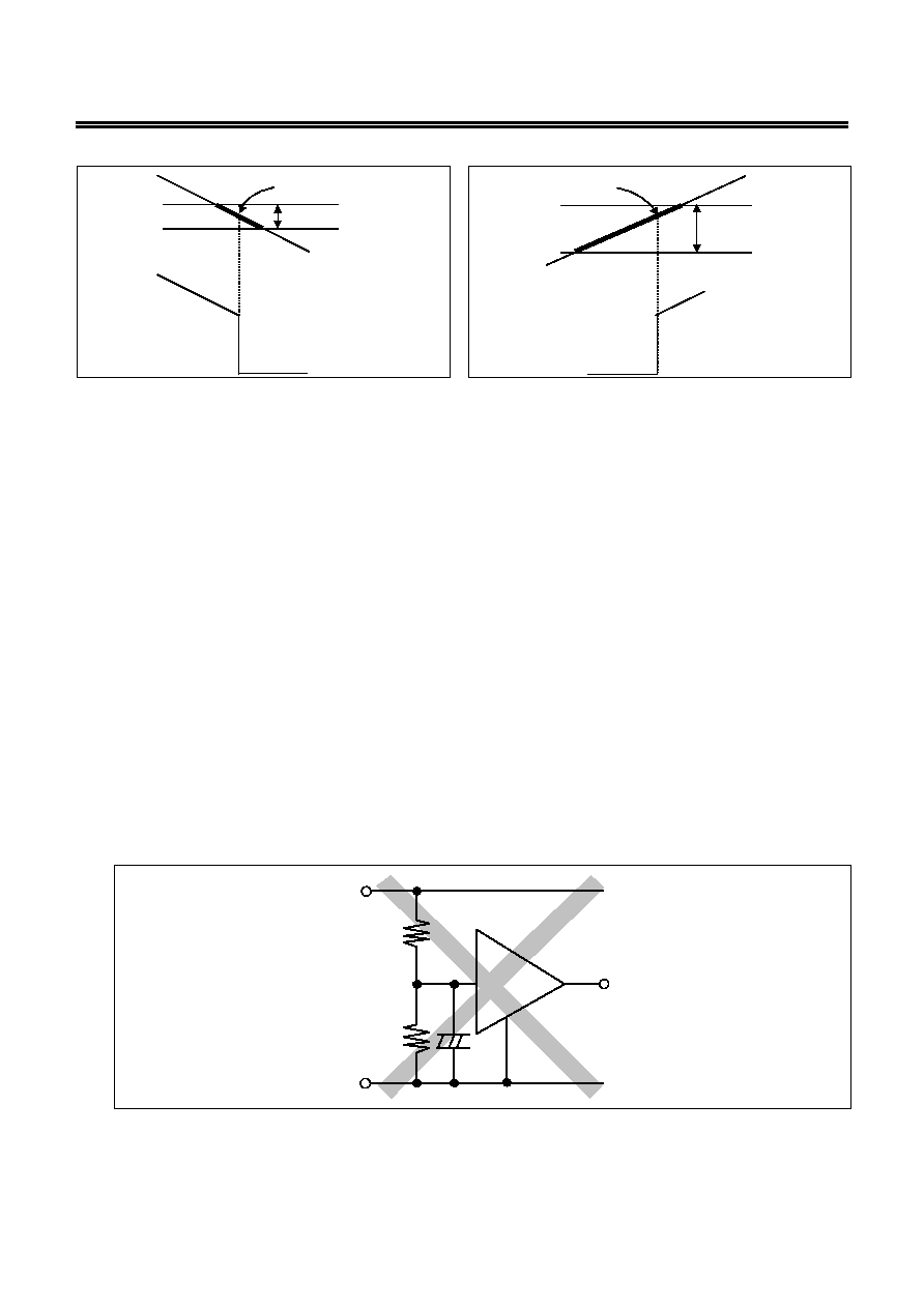
-V
DET
.
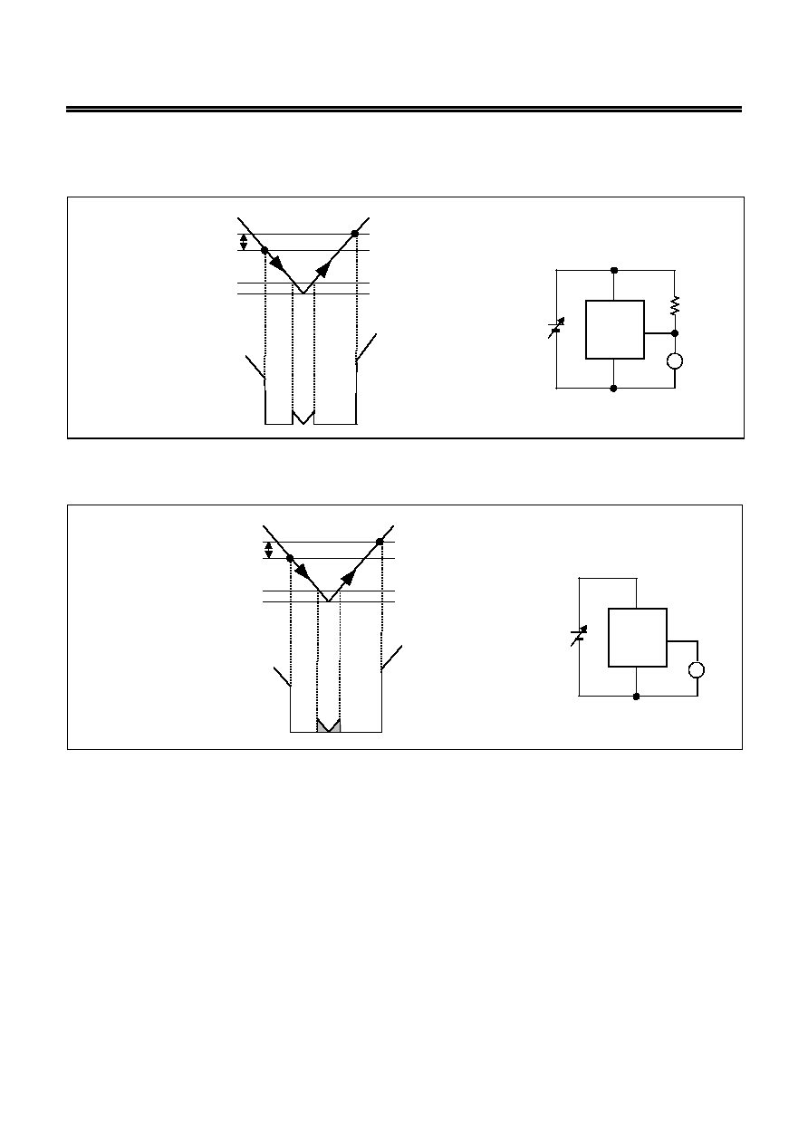
2. Hysteresis Width (V
HYS
)
The hysteresis width is the voltage difference between the detection voltage and the release voltage (The
voltage at point B
-The voltage at point A =V
HYS
in Figure 16). The existence of the hysteresis width
prevents malfunction caused by noise on input signal.
3. Through-type Current
The through-type current refers to the current that flows instantaneously at the time of detection and release
of a voltage detector. The through-type current is large in CMOS output products, small in Nch open-drain
output products.
4. Oscillation
In applications where a resistor is connected to the voltage detector input (Figure 13), taking a CMOS active
low product for example, the through-type current which is generated when the output goes from low to high
(release) causes a voltage drop equal to [through-type current]
◊[input resistance] across the resistor. When
the input voltage drops below the detection voltage (
-V
DET
) as a result, the output voltage goes to low level.
In this state, the through-type current stops and its resultant voltage drop disappears, and the output goes
from low to high. A through-type current is again generated, a voltage drop appears, and repeating the
process finally induces oscillation.
OUT
VSS
VDD
R
B
R
A
V
IN
S-808xxCL
Figure 21 An Example for Bad Implementation of Input Voltage Divider
ULTRA-SMALL PACKAGE HIGH-PRECISION VOLTAGE DETECTOR
S-808xxC Series
Rev.3.2
_00
24
Seiko Instruments Inc.
Electrical Characteristics for Customized Products
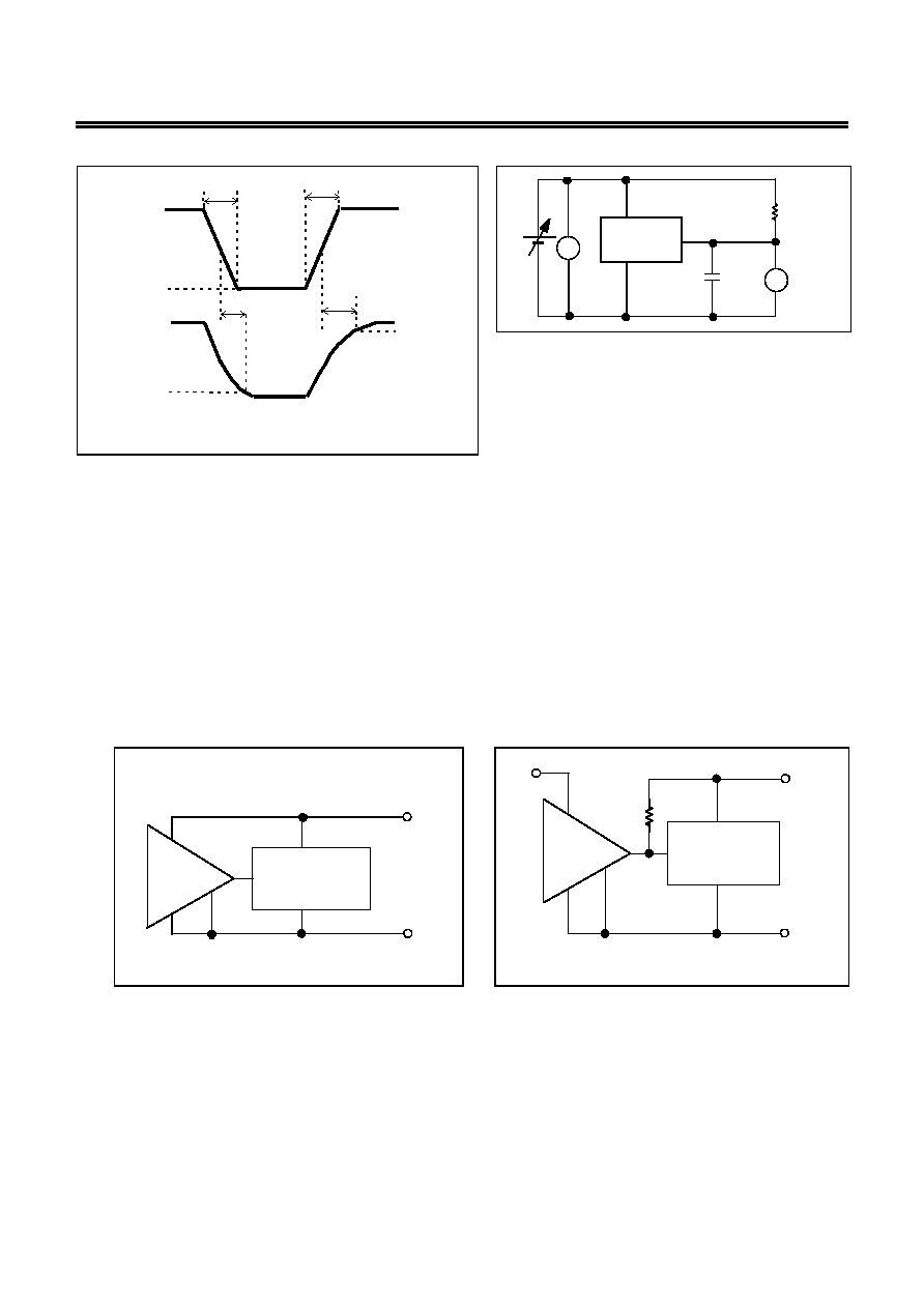
1. S-80824KNUA-D2B-T2, S-80824KNY-x
Table 18
(Ta
=25∞C unless otherwise specified)
Item Symbol Condition Min.
Typ.
Max.
Unit
Test
circuit
Detection voltage
*1
-V
DET
2.295
2.400
*2
2.505 V 1
Release voltage
+V
DET
4.300 4.400 4.500
Current consumption
I
SS
V
DD
=6.0 V
0.8 2.4
µA
2
Operating voltage
V
DD
0.95
10.0 V 1
Output current
I
OUT
V
DD
=0.95 V 0.03 0.24
mA 3
Output transistor,
Nch, V
DS
=0.5 V
V
DD
=1.2 V 0.23 0.50
Leakage current
I
LEAK
Output transistor,
Nch, V
DD
=10.0 V, V
DS
=10.0 V
0.1
µA
Response time
t
PLH
60
µs
1
Detection voltage
temperature
coefficient
*3
DET
DET
V
Ta
V
-
∑
-
Ta
=-40∞C to 85∞C
±100
±350 ppm/∞C
*1.
-V
DET
: Actual detection voltage value
*2.
Specified detection voltage value (
-V
DET(S)
)
*3.
The temperature change ratio in the detection voltage [mV/∞C] is calculated by using the following equation.
[
]
(
)
[ ]
[
]
1000
C
ppm/
V
Ta
V
V
Typ.
V
C
mV/
Ta
V
DET
DET
DET(S)
DET
˜
∞
-
-
◊
-
=
∞
-
∑
3
*
2
*
*1
*1.
Temperature change ratio of the detection voltage
*2.
Specified detection voltage
*3.
Detection voltage temperature coefficient
ULTRA-SMALL PACKAGE HIGH-PRECISION VOLTAGE DETECTOR
Rev.3.2
_00
S-808xxC Series
Seiko Instruments Inc.
25
2. S-80844KLUA-D2A-T2, S-80844KLY-x
Table 19
(Ta
=25∞C unless otherwise specified)
Item Symbol Condition Min.
Typ.
Max.
Unit
Test
circuit
Detection voltage
*1
-V
DET
4.295 4.450
*2
4.605
V
1
Release voltage
+V
DET
4.700
Current consumption
I
SS
V
DD
=6.0 V
1.0 3.0
µA
2
Operating voltage
V
DD
0.95
10.0 V 1
Output current
I
OUT
V
DD
=1.2 V
0.23 0.50
mA 3
Output transistor,
Nch, V
DS
=0.5 V V
DD
=2.4 V
1.60 3.70
Output transistor,
Pch, V
DS
=0.5 V
V
DD
=4.8 V
0.36 0.62
4
Response time
t
PLH
60
µs
1
Detection voltage
temperature
coefficient
*3
DET
DET
V
Ta
V
-
∑
-
Ta
=-40∞C to 85∞C
±100
±350 ppm/∞C
*1.
-V
DET
: Actual detection voltage value
*2.
Specified detection voltage value (
-V
DET(S)
)
*3.
The temperature change ratio in the detection voltage [mV/∞C] is calculated by using the following equation.
[
]
(
)
[ ]
[
]
1000
C
ppm/
V
Ta
V
V
Typ.
V
C
mV/
Ta
V
DET
DET
DET(S)
DET
˜
∞
-
-
◊
-
=
∞
-
∑
3
*
2
*
*1
*1.
Temperature change ratio of the detection voltage
*2.
Specified detection voltage
*3.
Detection voltage temperature coefficient

ULTRA-SMALL PACKAGE HIGH-PRECISION VOLTAGE DETECTOR
S-808xxC Series
Rev.3.2
_00
26
Seiko Instruments Inc.
3. S-80846KNUA-D2C-T2, S-80846KNY-x
Table 20
(Ta
=25∞C unless otherwise specified)
Item Symbol Condition Min.
Typ.
Max.
Unit
Test
circuit
Detection voltage
*1
-V
DET
4.500 4.600
*2
4.700 V 1
Hysteresis width
V
HYS
0.05
0.10
Current consumption
I
SS
V
DD
=6.0 V
0.9
2.7
µA
2
Operating voltage
V
DD
0.95
10.0 V 1
Output current
I
OUT
V
DD
=1.2 V
0.59 1.36
mA 3
Output transistor,
Nch, V
DS
=0.5 V V
DD
=2.4 V
2.88 4.98
Leakage current
I
LEAK
Output transistor,
Nch, V
DD
=10.0 V, V
DS
=10.0 V
0.1
µA
Response time
t
PLH
60
µs
1
Detection voltage
temperature
coefficient
*3
DET
DET
V
Ta
V
-
∑
-
Ta
=-40∞C to 85∞C
±100
±350 ppm/∞C
*1.
-V
DET
: Actual detection voltage value
*2.
Specified detection voltage value (
-V
DET(S)
)
*3.
The temperature change ratio in the detection voltage [mV/∞C] is calculated by using the following equation.
[
]
(
)
[ ]
[
]
1000
C
ppm/
V
Ta
V
V
Typ.
V
C
mV/
Ta
V
DET
DET
DET(S)
DET
˜
∞
-
-
◊
-
=
∞
-
∑
3
*
2
*
*1
*1.
Temperature change ratio of the detection voltage
*2.
Specified detection voltage
*3.
Detection voltage temperature coefficient
Precautions
∑ Do not apply an electrostatic discharge to this IC that exceeds the performance ratings of the built-in
electrostatic protection circuit.
∑ In CMOS output products of the S-808xxC series, the through-type current flows at the detection and the
release. If the input impedance is high, oscillation may occur due to the voltage drop by the through-type
current during releasing.
∑ In CMOS output products oscillation may occur when a pull-down resistor is used, and falling speed of the
power supply voltage (V
DD
) is slow near the detection voltage.
∑ When designing for mass production using an application circuit described herein, the product deviation and
temperature characteristics should be taken into consideration. SII shall not bear any responsibility for the
products on the circuits described herein.
∑ SII claims no responsibility for any and all disputes arising out of or in connection with any infringement of the
products including this IC upon patents owned by a third party.
ULTRA-SMALL PACKAGE HIGH-PRECISION VOLTAGE DETECTOR
Rev.3.2
_00
S-808xxC Series
Seiko Instruments Inc.
27
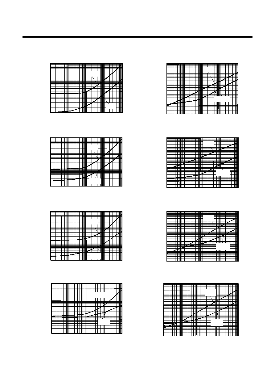
Typical Characteristics (Typical Data)
1. Detection Voltage (V
DET
) - Temperature (Ta)
0.75
0.80
0.85
0.90
-40
-20
0
20
40
60
80
Ta (∞C)
V
DE
T
(V)
S-80808CL
+V
DET
-V
DET
1.25
1.30
1.35
1.40
1.45
1.50
1.55
-40 -20 0 20 40 60 80
Ta (∞C)
V
DE
T
(V)
S-80814CL
+V
DET
-V
DET
1.45
1.50
1.55
1.60
-40
-20
0
20
40
60
80
Ta (∞C)
V
DET
(V)
S-80815CL
+V
DET
-V
DET
5.80
5.90
6.00
6.10
6.20
6.30
6.40
-40 -20 0 20 40 60 80
Ta (∞C)
V
DET
(V
)
S-80860CL
+V
DET
-V
DET
2. Hysteresis Voltage Width (V
HYS
) - Temperature (Ta)
3.0
4.0
5.0
6.0
8.0
-40 -20 0 20 40 60 80
Ta (∞C)
V
HYS
(%
)
S-80808CL
7.0
3.0
4.0
5.0
6.0
8.0
-40 -20 0 20 40 60 80
Ta (∞C)
V
HYS
(%)
S-80814CL
7.0
3.0
4.0
5.0
6.0
8.0
-40 -20 0 20 40 60 80
Ta (∞C)
V
HYS
(%
)
S-80815CL
7.0
4.0
5.0
6.0
7.0
8.0
-40 -20 0 20 40 60 80
Ta (∞C)
V
HY
S
(%)
S-80860CL
3.0
ULTRA-SMALL PACKAGE HIGH-PRECISION VOLTAGE DETECTOR
S-808xxC Series
Rev.3.2
_00
28
Seiko Instruments Inc.
3. Current Consumption (I
SS
) - Input Voltage (V
DD
)
0.0
0.5
1.0
1.5
2.0
2.5
3.0
3.5
4.0
4.5
0 1.0
2.0
3.0
4.0
5.0
6.0
V
DD
(V)
I
SS
(
µ
A
)
S-80808CL
9.3
µA
Ta=25∞C
0.0
0.5
1.0
1.5
2.0
2.5
3.0
3.5
4.0
4.5
0 1.0
2.0
3.0
4.0
5.0
6.0
V
DD
(V)
S-80814CL
21.5
µA
Ta=25∞C
I
SS
(
µ
A
)
0.0
0.2
0.4
0.6
0.8
1.0
1.2
1.4
1.6
1.8
0 2.0 4.0 6.0 8.0 10.0
12.0
V
DD
(V)
I
SS
(
µ
A
)
S-80815CL
4.7
µA
Ta=25∞C
0.0
0.2
0.4
0.6
0.8
1.0
1.2
1.4
1.6
1.8
0 2.0
4.0
6.0 8.0
10.0
12.0
V
DD
(V)
S-80860CL
12.8
µA
Ta=25∞C
I
SS
(
µ
A
)
4. Current Consumption (I
SS
) - Temperature (Ta)
0.0
0.5
1.0
1.5
2.0
-40 -20 0 20 40 60 80
Ta (∞C)
I
SS
(
µ
A
)
S-80808CL
V
DD
=1.5 V
0.0
0.5
1.0
1.5
2.0
-40 -20 0 20 40 60 80
Ta (∞C)
I
SS
(
µ
A
)
S-80814CL
V
DD
=2.0 V
0.0
0.5
1.0
1.5
2.0
-40 -20 0 20 40 60 80
Ta (∞C)
I
SS
(
µ
A
)
S-80815CL
V
DD
=3.5 V
0.0
0.5
1.0
1.5
2.0
-40 -20 0 20 40 60 80
Ta (∞C)
I
SS
(
µ
A
)
S-80860CL
V
DD
=7.5 V
ULTRA-SMALL PACKAGE HIGH-PRECISION VOLTAGE DETECTOR
Rev.3.2
_00
S-808xxC Series
Seiko Instruments Inc.
29
5. Nch Transistor Output Current (I
OUT
) ≠ V
DS
0
1.0
2.0
3.0
4.0
5.0
0 0.5
1.0 1.5 2.0 2.5
V
DS
(V)
I
OU
T
(mA
)
S-80814CL/CN
Ta=25∞C
V
DD
=0.7 V
V
DD
=1.0
V
DD
=1.3 V
0
10
20
30
40
50
0 1.0 2.0 3.0 4.0 5.0
V
DS
(V)
I
OUT
(mA
)
6.0 V
S-80860CL/CN
Ta=25∞C
V
DD
=1.2 V
2.4 V
3.6 V
4.8 V
6. Pch Transistor Output Current (I
OUT
) -V
DS
S-80808CL
0
1.0
2.0
3.0
4.0
5.0
0 0.5 1.0 1.5 2.0 2.5
V
DS
(V)
I
OUT
(m
A
)
Ta=25∫C
V
DD
=2.9V
V
DD
=2.4V
V
DD
=1.4 V
V
DD
=0.9 V
V
DD
=1.9 V
S-80815CL
0
5
10
15
20
25
30
0 2.0 4.0 6.0 8.0
10.0
V
DS
(V)
I
OUT
(mA
)
Ta=25∫C
8.4 V
7.2 V
6.0 V
3.6 V
V
DD
=2.4 V
4.8 V
7. Nch Transistor Output Current (I
OUT
) - Input Voltage (V
DD
)
0
1.5
3.0
4.5
6.0
0 0.5
1.0
1.5
2.0
V
DD
(V)
I
OU
T
(mA)
S-80814CL/CN
V
DS
=0.5 V
Ta=85∞
Ta=-40∞C
Ta=25∞C
0
5
10
15
20
0 2.0 4.0 6.0 8.0
V
DD
(V)
I
OU
T
(m
A
)
S-80860CL/CN
V
DS
=0.5 V
Ta=-40∞C
Ta=25∞C
Ta=85∞C
8. Pch Transistor Output Current (I
OUT
) - Input Voltage (V
DD
)
0
0.5
1.0
1.5
2.0
2.5
3.0
0 1.0 2.0 3.0 4.0 5.0 6.0
V
DD
(V)
I
OUT
(mA
)
S-80808CL
V
DS
=0.5 V
Ta=-40∞C
Ta=25∞C
Ta=85∞C
0
1
2
3
4
5
6
0 2.0
4.0
6.0 8.0
10.0
12.0
V
DD
(V)
I
OUT
(m
A
)
S-80815CL
V
DS
=0.5 V
Ta=-40∞C
Ta=25∞C
Ta=85∞C
ULTRA-SMALL PACKAGE HIGH-PRECISION VOLTAGE DETECTOR
S-808xxC Series
Rev.3.2
_00
30
Seiko Instruments Inc.
9. Minimum Operating Voltage - Input Voltage (V
DD
)
0.0
0.3
0.6
0.9
1.2
0.0 0.2 0.4 0.6
1.0
V
DD
(V)
V
OU
T
(V)
S-80808CN
Pull-up to V
DD
100 k
Ta=-40∞C
Ta=25∞C
Ta=85∞C
0.8
0.0
1.0
2.0
3.0
4.0
0.2
0.4 0.6
0.8 1.0
V
DD
(V)
V
OU
T
(V)
S-80808CN
Pull-up to 3 V
Ta=-40∞C
Ta=25∞C
Ta=85∞C
0.0
0.5
1.0
1.5
2.0
0 0.5 1.0
1.5 2.0
V
DD
(V)
V
OU
T
(V)
S-80815CN
Pull-up to V
DD
100 k
Ta=-40∞C
Ta=25∞C
Ta=85∞C
0.0
1.0
2.0
3.0
4.0
0 0.5
1.0
1.5 2.0
V
DD
(V)
V
OU
T
(V
)
S-80815CN
Pull-up to 3 V
Ta=-40∞C
Ta=25∞C
Ta=85∞C
V
OUT
(V)
PULL-UP
PULL-UP
◊0.1
0
V
DD
(V)
V
DDmin
0.30
0.35
0.40
0.45
0.50
0.55
0.60
0.65
1.0 1.5 2.0 2.5 3.0 3.5 4.0 4.5 5.0 5.5
PULL-UP (V)
V
DD
m
i
n
(V
)
S-80808CN
Pull-up to V
DD
:100 k
Ta=-40∞C
Ta=25∞C
Ta=85∞C
Remark
V
DDmin.
is defined by the V
DD
voltage at which
V
OUT
goes below 10
% of PULL-UP
voltage when the V
DD
increase
from 0 V.
0.40
0.45
0.50
0.55
0.60
0.65
0.70
0.75
3.0 4.0 5.0 6.0 7.0 8.0 9.0 10.0 11.0 12.0
PULL-UP (V)
V
DDmin
(V
)
S-80815CN
Pull-up to V
DD
:100 k
Ta=-40∞C
Ta=25∞C
Ta=85∞C
Figure 22
ULTRA-SMALL PACKAGE HIGH-PRECISION VOLTAGE DETECTOR
Rev.3.2
_00
S-808xxC Series
Seiko Instruments Inc.
31
10. Dynamic Response - C
OUT
0.001
0.01
0.1
1
0.00001 0.0001 0.001
0.01
0.1
Load capacitance (
µF)
R
e
sp
on
se
t
i
m
e
(m
s)
S-80808CL
Ta=25∞C
t
pLH
t
pHL
0.001
0.01
0.1
1
10
100
0.00001 0.0001 0.001 0.01
0.1
Load capacitance (
µF)
R
e
sop
n
se
t
i
m
e
(m
s)
S-80808CN
Ta=25∞C
t
pHL
t
pLH
0.001
0.01
0.1
1
0.00001 0.0001 0.001 0.01
0.1
Load capacitanse (
µF)
R
e
sp
on
se
t
i
m
e
(m
s)
S-80814CL
Ta=25∞C
t
pLH
t
pHL
0.001
0.01
0.1
1
10
100
0.00001 0.0001 0.001
0.01
0.1
Load Capacitance (
µF)
Re
s
p
on
se t
i
m
e
(m
s)
S-80814CN
Ta=25∞C
t
pHL
t
pLH
0.001
0.01
0.1
1
0.00001 0.0001 0.001
0.01
0.1
Load Capacitance (
µF)
Re
s
pons
e tim
e
(
m
s
)
S-80815CL
Ta=25∞C
t
pLH
t
pHL
0.001
0.01
0.1
1
10
100
0.00001 0.0001 0.001 0.01
0.1
Load Capacitance (
µF)
R
e
s
pons
e
tim
e
(
m
s
)
S-80815CN
Ta=25∞C
t
pHL
t
pLH
0.001
0.01
0.1
1
0.00001 0.0001 0.001 0.01
0.1
Load Capacitance (
µF)
R
e
sp
o
n
s
e
t
i
m
e
(m
s)
S-80860CL Ta=25∞C
t
pLH
t
pHL
0.001
0.01
0.1
1
10
100
0.00001 0.0001 0.001
0.01
0.1
Load Capacitance (
µF)
R
e
spone tim
e
(m
s)
S-80860CN
Ta=25∞C
t
pHL
t
pLH
ULTRA-SMALL PACKAGE HIGH-PRECISION VOLTAGE DETECTOR
S-808xxC Series
Rev.3.2
_00
32
Seiko Instruments Inc.
OUT
VSS
VDD
S-808xxC
Series
V
R
*1
100 k
C
OUT
V
DD
V
V
IH
Output voltage
Input voltagae
V
IL
V
DD
t
pHL
t
pLH
V
IH
=10 V, V
IL
=0.95 V
1
µs
1
µs
V
DD
◊10 %
V
DD
◊90 %
*1.
R is unnecessary for CMOS output products.
Figure 23 Measurement Condition for Response Time
Figure 24 Measurement Circuit for Response Time
Caution The above connection diagram and constants do not guarantee correct operation. Perform
sufficient evaluation using the actual application to set the constants.
Application Circuit Examples
1. Microcomputer Reset Circuits
If the power supply voltage to a microcomputer falls below the specified level, an unspecified operation may
be performed or the contents of the memory register may be lost. When power supply voltage returns to
normal, the microcomputer needs to be initialized before normal operations can be done.
Reset circuits protect microcomputers in the event of current being momentarily switched off or lowered.
Reset circuits shown in Figures 25 to 26 can be easily constructed with the help of the S-808xxC series,
that has low operating voltage, a high-precision detection voltage and hysteresis.
VSS
VDD
Microcomputer
S-
808xxCL
VSS
(Only for Nch open-drain products)
VDD1
VDD2
Microcomputer
S-
808xxCN
Figure 25 Reset Circuit Example(S-808xxCL)
Figure 26 Reset Circuit Example (S-808xxCN)
Caution The above connection diagram and constants do not guarantee correct operation. Perform
sufficient evaluation using the actual application to set the constants.
ULTRA-SMALL PACKAGE HIGH-PRECISION VOLTAGE DETECTOR
Rev.3.2
_00
S-808xxC Series
Seiko Instruments Inc.
33
2. Power-on Reset Circuit
A power-on reset circuit can be constructed using Nch open-drain output product of S-808
◊◊C Series.
(
Nch open-drain products)
OUT
VIN
VSS
VDD
S-
808xxCN
R
*1
C
Di
*2
(R
75 k)
*1.
Resistor R should be 75 k
or less to prevent oscillation.
*2.
Diode Di instantaneously discharges the charge stored in the capacitor (C) at the power falling,Di can be
removed when the delay of the falling time is not important.
Figure 27
V
DD
(V)
t (s)
OUT
(V)
t (s)
Figure 28
Remark
When the power rises sharply as shown in the Figure 29 left, the output may goes to the high level
for an instant in the undefined region where the output voltage is undefined since the power
voltage is less than the minimum operation voltage.
V
DD
(V)
t (s)
OUT
(V)
t (s)
Figure 29
ULTRA-SMALL PACKAGE HIGH-PRECISION VOLTAGE DETECTOR
S-808xxC Series
Rev.3.2
_00
34
Seiko Instruments Inc.
3. Change of Detection Voltage
In Nch open-drain output products of the S-808xxC series, detection voltage can be changed using
resistance dividers or diodes as shown in Figures 30 to 31. In Figure 30, hysteresis width also changes.
(Nch open-drain
output products)
R
A
*1
OUT
VIN
VSS
VDD
+
-
S-
808xxCN
R
B
(RA
75 k)
DET
B
B
A
V
R
R
R
voltagae
Detection
-
∑
+
=
HYS
B
B
A
V
R
R
R
width
Hysterisis
∑
+
=
(Nch open-drain
output product)
V
f1
OUT
VIN
VSS
VDD
S-
808xxCN
V
f2
Detection voltage=V
f1
+V
f2
+(
-V
DET
)
*1.
R
A
should be 75 k
or less to prevent oscillation.
Caution If R
A
and R
B
are large, the hysteresis
width may aloso be larger than the value
given by the above equation due to the
through-type current (which flows
slightly in an Nch open-drain product).
Figure 30
Figure 31
Caution The above connection diagram and constants do not guarantee correct operation. Perform
sufficient evaluation using the actual application to set the constants.
No.
TITLE
SCALE
UNIT
mm
Seiko Instruments Inc.
0.3
+0.1
-0.05
0.4
+0.1
-0.05
0.05
1
2
4
3
0.16
+0.1
-0.06
1.3±0.2
2.0±0.2
No. NP004-A-P-SD-1.1
SC82AB-A-PKG Dimensions
NP004-A-P-SD-1.1

No.
TITLE
SCALE
UNIT
mm
Seiko Instruments Inc.
1.1±0.1
0.2±0.05
4.0±0.1
2.0±0.05
4.0±0.1
1.5
1.05±0.1
+0.1
-0.05
2.2±0.2
(0.7)
No. NP004-A-C-SD-2.1
NP004-A-C-SD-2.1
SC82AB-A-Carrier Tape
Feed direction
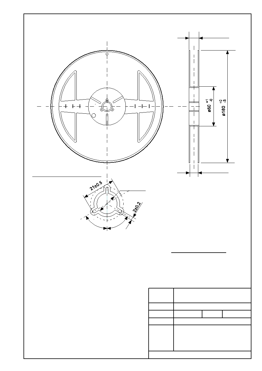
No.
TITLE
SCALE
UNIT
mm
Seiko Instruments Inc.
QTY.
3,000
(60∞)
(60∞)
¯13±0.2
12.5max.
9.0±0.3
No. NP004-A-R-SD-1.1
NP004-A-R-SD-1.1
SC82AB-A-Reel
Enlarged drawing in the central part

No.
TITLE
SCALE
UNIT
mm
Seiko Instruments Inc.
2.9±0.2
1.9±0.2
0.95±0.1
0.4±0.1
0.16
+0.1
-0.06
1
2
3
4
5
No. MP005-A-P-SD-1.2
MP005-A-P-SD-1.2
SOT235-A-PKG Dimensions

No.
TITLE
SCALE
UNIT
mm
Seiko Instruments Inc.
¯1.5
+0.1
-0
2.0±0.05
¯1.0
+0.2
-0
4.0±0.1
1.4±0.2
0.25±0.1
3.2±0.2
1
2
3
4
5
No. MP005-A-C-SD-2.1
MP005-A-C-SD-2.1
SOT235-A-Carrier Tape
Feed direction
4.0±0.1(10 pitches:40.0±0.2)
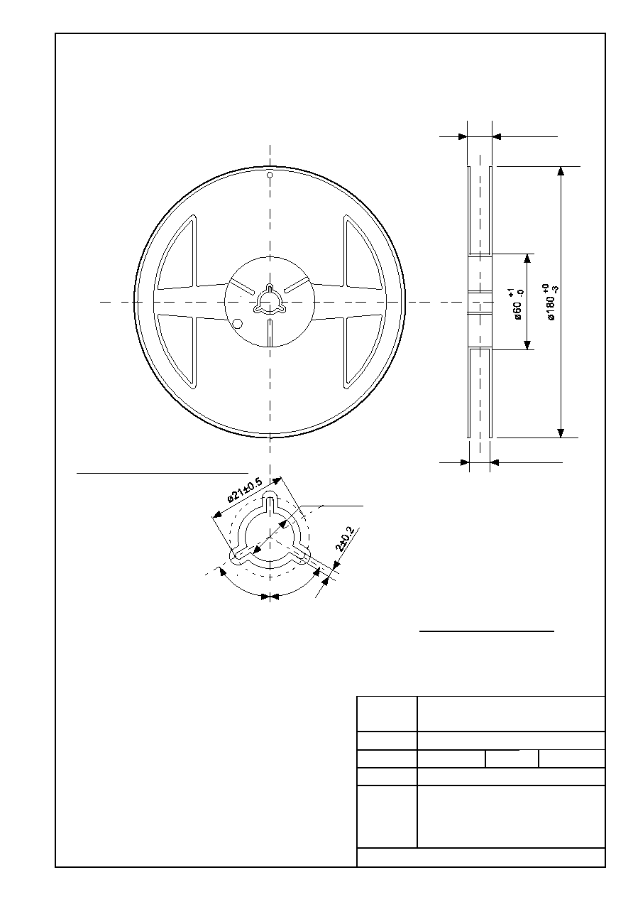
No.
TITLE
SCALE
UNIT
mm
Seiko Instruments Inc.
12.5max.
9.0±0.3
¯13±0.2
(60∞)
(60∞)
QTY.
3,000
No. MP005-A-R-SD-1.1
MP005-A-R-SD-1.1
SOT235-A-Reel
Enlarged drawing in the central part
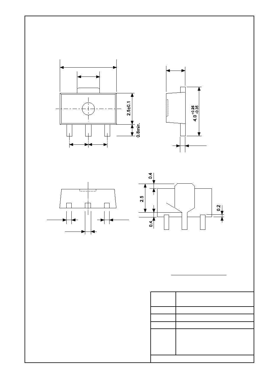
No.
TITLE
SCALE
UNIT
mm
Seiko Instruments Inc.
0.4±0.05
1.5±0.1
4.5±0.1
1.6±0.2
1.5±0.1 1.5±0.1
0.45±0.1
0.4±0.1
0.4±0.1
45∞
3
1
2
No. UP003-A-P-SD-1.1
UP003-A-P-SD-1.1
SOT893-A-PKG Dimensions
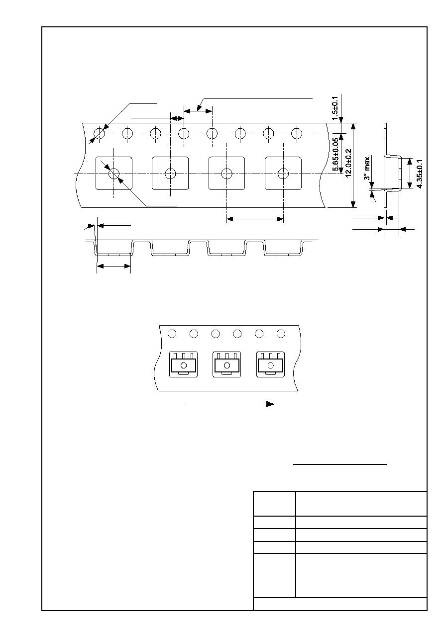
No.
TITLE
SCALE
UNIT
mm
Seiko Instruments Inc.
2.0±0.1
0.3±0.05
8.0±0.1
¯1.5
+0.1
-0
2.0±0.05
¯1.5
+0.1
-0
4.75±0.1
5∞ max.
No. UP003-A-C-SD-1.1
UP003-A-C-SD-1.1
SOT893-A-Carrier Tape
Feed direction
4.0±0.1(10 pitches : 40.0±0.2)
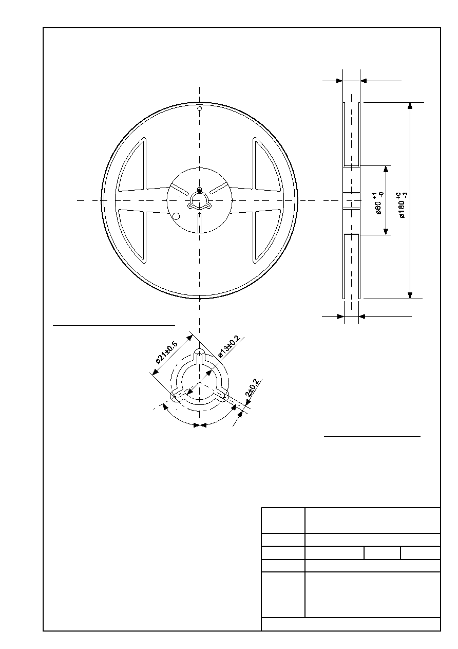
No.
TITLE
SCALE
UNIT
mm
Seiko Instruments Inc.
13.0±0.3
16.5max.
(60∞)
(60∞)
QTY.
1,000
No. UP003-A-R-SD-1.1
UP003-A-R-SD-1.1
SOT893-A-Reel
Enlarged drawing in the central part
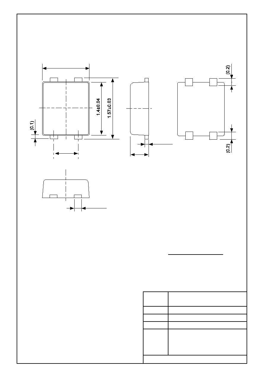
1.2±0.04
0.65
0.2±0.05
0.48±0.02
0.08
No.
TITLE
SCALE
UNIT
mm
Seiko Instruments Inc.
SNT-4A-A-PKG Dimensions
PF004-A-P-SD-3.0
No. PF004-A-P-SD-3.0
+0.05
-0.02

No.
TITLE
SCALE
UNIT
mm
Seiko Instruments Inc.
PF004-A-C-SD-1.0
SNT-4A-A-Carrier Tape
Feed direction
TF type
4.0±0.1
2.0±0.05
4.0±0.1
¯1.5
+0.1
-0
¯0.5
1.45±0.1
0.65±0.05
0.25±0.05
1
2
3
4
5∞
No. PF004-A-C-SD-1.0
+0.1
-0
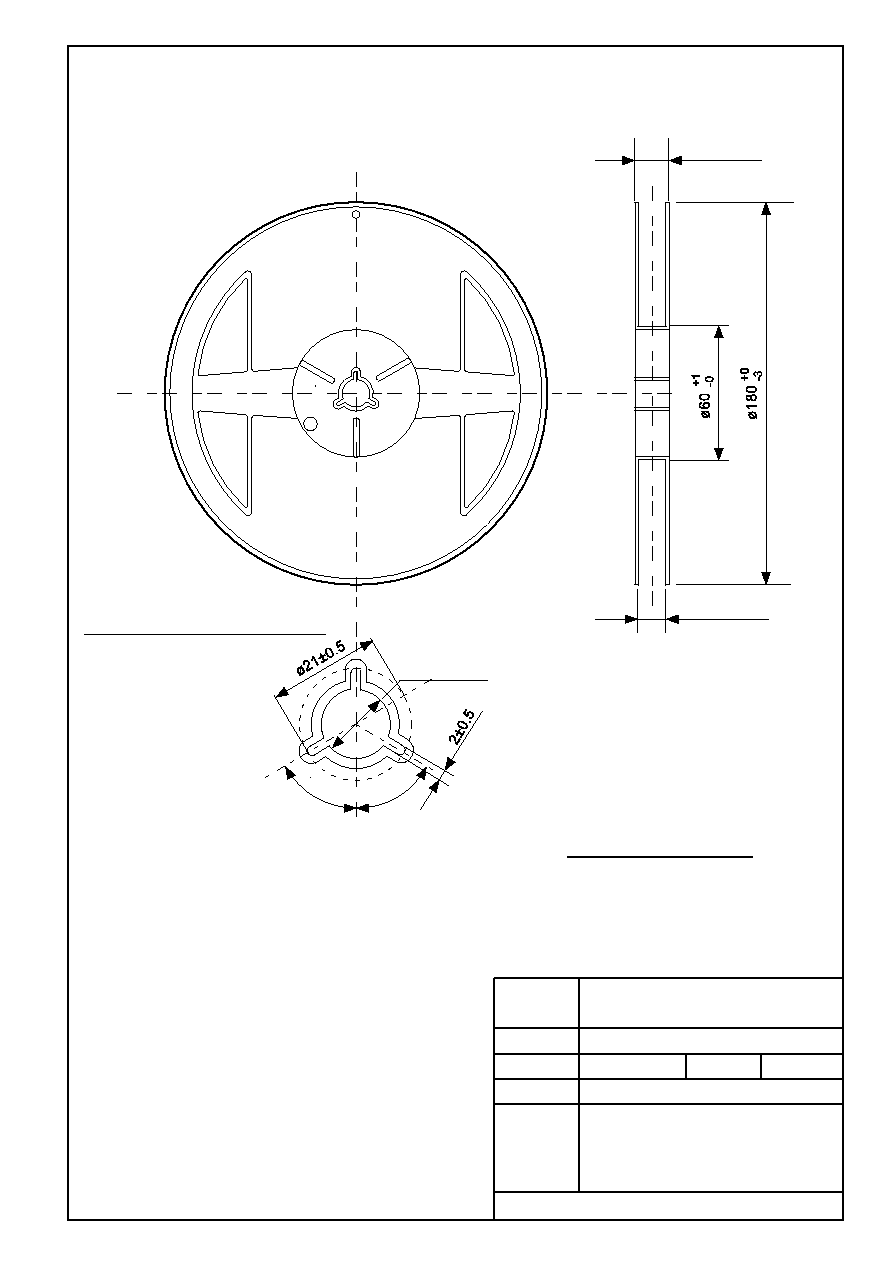
12.5max.
9.0±0.3
¯13±0.2
(60∞)
(60∞)
QTY.
5,000
No. PF004-A-R-SD-1.0
PF004-A-R-SD-1.0
Enlarged drawing in the central part
No.
TITLE
SCALE
UNIT
mm
Seiko Instruments Inc.
SNT-4A-A-Reel

No.
TITLE
SCALE
UNIT
mm
Seiko Instruments Inc.
5.2max.
4.2max.
0.6max.
0.45±0.1
0.45±0.1
1.27
No. YS003-B-P-SD-1.1
YS003-B-P-SD-1.1
TO92-B-PKG Dimensions
Marked side

No.
TITLE
SCALE
UNIT
mm
Seiko Instruments Inc.
4.2max.
0.45±0.1
Marked side
1.27
5.2max.
0.45±0.1
0.6max.
2.5
+0.4
-0.1
No. YF003-A-P-SD-1.1
YF003-A-P-SD-1.1
TO92-A-PKG Dimensions
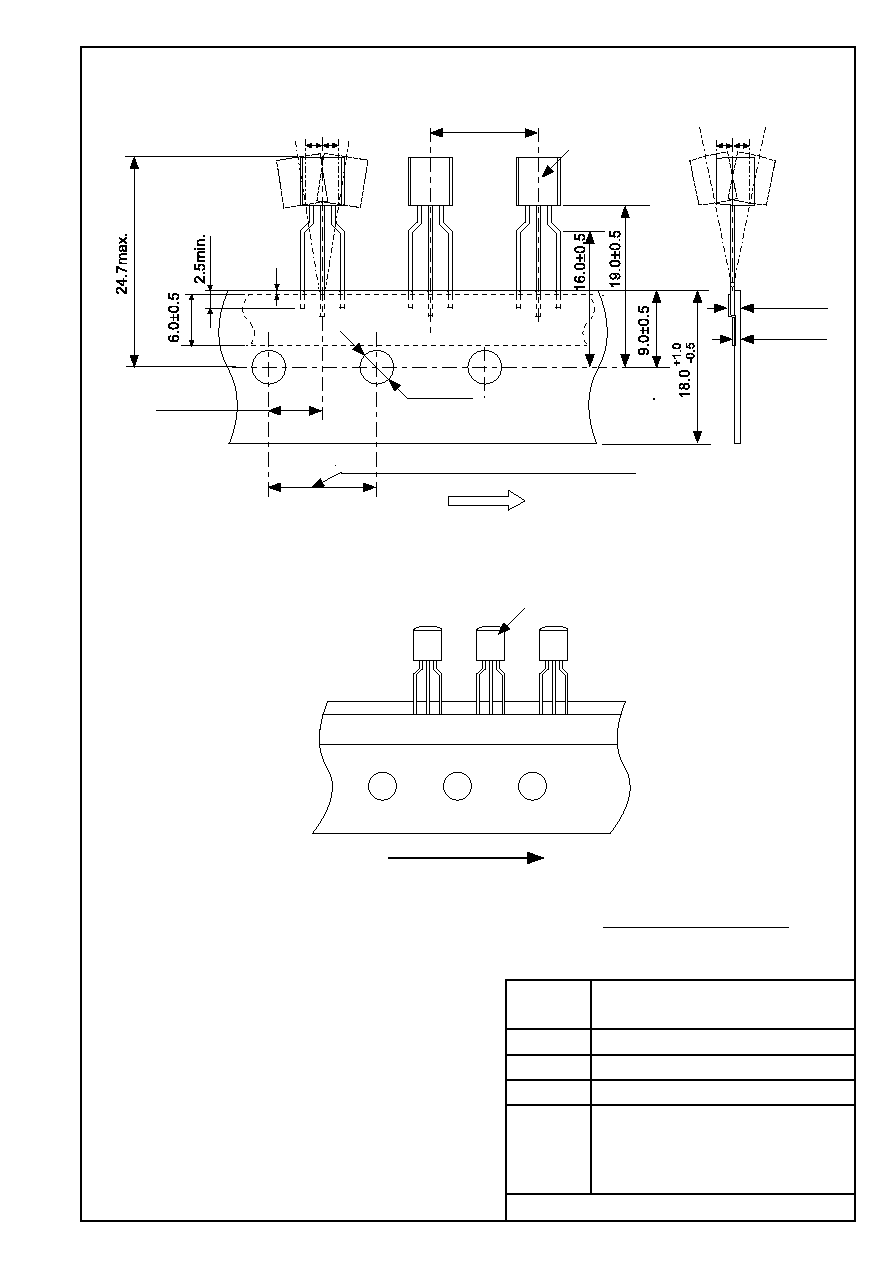
No.
TITLE
SCALE
UNIT
mm
Seiko Instruments Inc.
12.7±1.0
6.35±0.4
¯4.0±0.2
0.5max.
1#pin
3#pin
1.0max.
1.0max.
0.7±0.2
1.45max.
No. YF003-A-C-SD-4.1
YF003-A-C-SD-4.1
TO92-A-Radial Tape
Marked side
12.7±0.3(20 pitches : 254.0±1.0)
Feed direction
Feed direction
Marked side
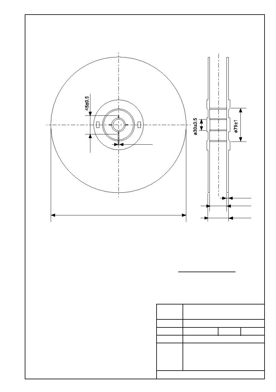
No.
TITLE
SCALE
UNIT
mm
Seiko Instruments Inc.
¯358±2
43±0.5
53±0.5
5±0.5
2±0.5
QTY.
2,000
No. YF003-A-R-SD-2.1
YF003-A-R-SD-2.1
TO92-A-Reel
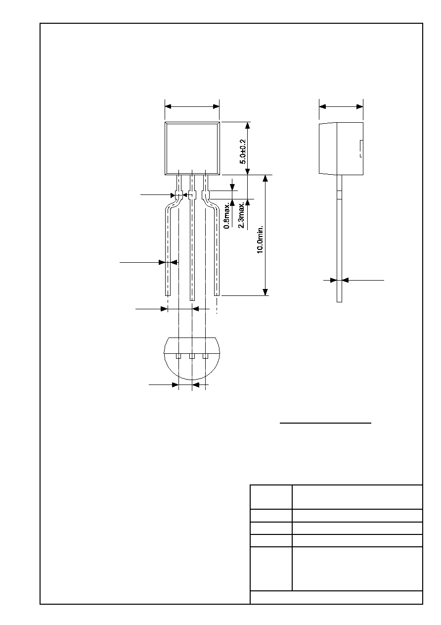
No.
TITLE
SCALE
UNIT
mm
Seiko Instruments Inc.
4.2max.
0.45±0.1
Marked side
1.27
5.2max.
0.45±0.1
0.6max.
2.5
+0.4
-0.1
No. YF003-A-P-SD-1.1
YF003-A-P-SD-1.1
TO92-A-PKG Dimensions

No.
TITLE
SCALE
UNIT
mm
Seiko Instruments Inc.
12.7±1.0
6.35±0.4
¯4.0±0.2
0.5max.
1#pin
3#pin
1.0max.
1.0max.
0.7±0.2
1.45max.
Feed direction
12.7±0.3(20 pitches : 254.0±1.0)
Marked side
No. YZ003-C-C-SD-3.1
YZ003-C-C-SD-3.1
TO92-C-Radial Tape
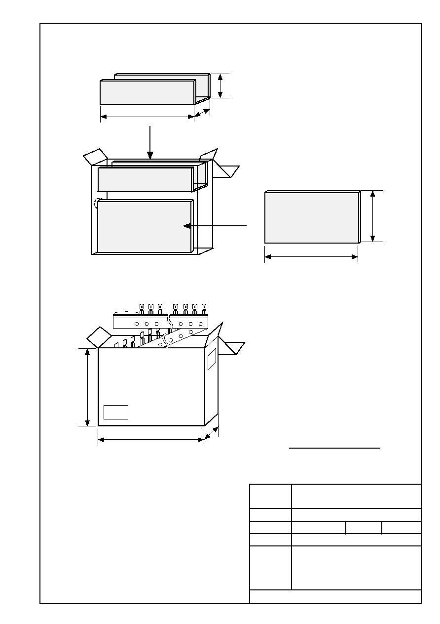
No.
TITLE
SCALE
UNIT
mm
Seiko Instruments Inc.
330
47
262
Spacer
320
40
60
165
320
QTY.
2,500
No. YZ003-C-Z-SD-2.1
YZ003-C-Z-SD-2.1
Side spacer placed in front side
Space more than 4 strokes
TO92-C-Ammo Packing

∑
The information described herein is subject to change without notice.
∑
Seiko Instruments Inc. is not responsible for any problems caused by circuits or diagrams described herein
whose related industrial properties, patents, or other rights belong to third parties. The application circuit
examples explain typical applications of the products, and do not guarantee the success of any specific
mass-production design.
∑
When the products described herein are regulated products subject to the Wassenaar Arrangement or other
agreements, they may not be exported without authorization from the appropriate governmental authority.
∑
Use of the information described herein for other purposes and/or reproduction or copying without the
express permission of Seiko Instruments Inc. is strictly prohibited.
∑
The products described herein cannot be used as part of any device or equipment affecting the human
body, such as exercise equipment, medical equipment, security systems, gas equipment, or any apparatus
installed in airplanes and other vehicles, without prior written permission of Seiko Instruments Inc.
∑
Although Seiko Instruments Inc. exerts the greatest possible effort to ensure high quality and reliability, the
failure or malfunction of semiconductor products may occur. The user of these products should therefore
give thorough consideration to safety design, including redundancy, fire-prevention measures, and
malfunction prevention, to prevent any accidents, fires, or community damage that may ensue.