 | –≠–ª–µ–∫—Ç—Ä–æ–Ω–Ω—ã–π –∫–æ–º–ø–æ–Ω–µ–Ω—Ç: S-812XXSG | –°–∫–∞—á–∞—Ç—å:  PDF PDF  ZIP ZIP |

Contents
Features .............................................................................................. 1
Applications ......................................................................................... 1
Pin Assignment ................................................................................... 1
Block Diagram ..................................................................................... 1
Selection Guide ................................................................................... 2
Absolute Maximum Ratings ................................................................. 2
Electrical Characteristics ..................................................................... 3
Test Circuits ........................................................................................ 11
Technical Terms .................................................................................. 12
Operation............................................................................................. 13
Transient Response ............................................................................ 14
Standard Circuit................................................................................... 17
Application Circuits .............................................................................. 17
Notes on Design .................................................................................. 19
Dimensions.......................................................................................... 20
Markings.............................................................................................. 20
Package Power Dissipation ................................................................. 21
Taping Dimensions.............................................................................. 22
Characteristics..................................................................................... 25
Measuring Circuits............................................................................... 31
Frequently Asked Questions................................................................ 32
Seiko Instruments Inc.
1
The S-812XXSG Series is a three-terminal positive voltage regulator
made using the CMOS process. Since the S-812XXSG Series has
higher precision output voltage and consumes less current than existing
three-terminal voltage regulators, battery-powered portable equipment
can have a higher performance and a longer service life.
Applications
Constant voltage power supply of battery-powered equipment, communications equipment, video equipment
and others
Pin Assignment
HIGH-PRECISION
VOLTAGE REGULATOR
S-812XXSG Series
Features
Low power consumption (2.5
A max.)
High accuracy of output voltage
±2% : V
OUT
2.7 V
±2.4% : V
OUT
2.6 V
Small input/output voltage difference
(S-81250SG: 160 mV typ. I
OUT
=10 mA)
Low temperature coefficient of output voltage
(S-81250SG: ±0.625 mV/
C typ.)
Wide operating voltage range
(S-81250SG: 16 V max.)
Good line regulation
(S-81250SG: 40 mV typ. I
OUT
=1
A to 40 mA)
TO-92, SOT-89-3 and SOT-23-5 package
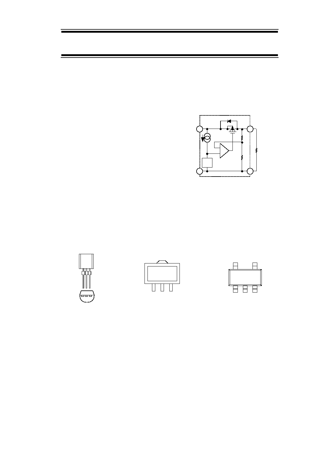
Block Diagram
Figure 1
R
L
GND
V
IN
V
OUT
2
+
-
*
Ref.
vol.
3
1
* Parasitic diode
Bottom view
1 2 3
(1)
TO-92
1 GND
2 V
IN
3 V
OUT
Top view
1
2
3
1 GND
2 V
IN
3 V
OUT
(2)
SOT-89-3
GND
V
IN
V
OUT
NC
NC
Top View
(3)
SOT-23-5
Figure 2

HIGH PRECISION VOLTAGE REGULATOR
S-812XXSG Series
2
Seiko Instruments Inc.
Selection Guide
Table 1
Output voltage
TO-92 *1
SOT-89-3 *2
SOT-23-5 *2
1.1
2.4%
S-81211SGY-X
S-81211SGUP-DQA-X
S-81211SG-QA-X
1.5
2.4%
S-81215SGY-X
S-81215SGUP-DQK-X
S-81215SG-QK-X
1.7
2.4%
S-81217SG-QQ-X
1.8
2.4%
S-81218SG-QR-X
2.0
2.4%
S-81220SGY-X
S-81220SGUP-DQS-X
S-81220SG-QS-X
2.1
2.4%
S-81221SGUP-DQU-X
2.3
2.4%
S-81223SGY-X
S-81223SG-QW-X
2.4
2.4%
S-81224SGY-X
S-81224SGUP-DQX-X
S-81224SG-QX-X
2.5
2.4%
S-81225SGY-X
S-81225SGUP-DQH-X
S-81225SG-QH-X
2.7
2.0%
S-81227SGUP-DQZ-X
3.0
2.0%
S-81230SGY-X
S-81230SGUP-DQB-X
S-81230SG-QB-X
3.3
2.0%
S-81233SGY-X
S-81233SGUP-DQF-X
S-81233SG-QF-X
3.5
2.0%
S-81235SGY-X
S-81235SGUP-DQI-X
S-81235SG-QI-X
3.6
2.0%
S-81236SGUP-DQ7-X
3.7
2.0%
S-81237SGY-X
S-81237SGUP-DQE-X
S-81237SG-QE-X
4.0
2.0%
S-81240SGY-X
S-81240SGUP-DQJ-X
S-81240SG-QJ-X
4.2
2.0%
S-81242SG-IB-X
4.5
2.0%
S-81245SGY-X
S-81245SGUP-DQ5-X
S-81245SG-Q5-X
4.6
2.0%
S-81246SGY-X
S-81246SGUP-DQM-X
S-81246SG-QM-X
4.7
2.0%
S-81247SG-IE-X
5.0
2.0%
S-81250SGY-X
S-81250SGUP-DQD-X
S-81250SG-QD-X
5.2
2.0%
S-81252SGY-X
S-81252SGUP-DQL-X
S-81252SG-QL-X
5.3
2.0%
S-81253SGUP-DIJ-X
5.4
2.0%
S-81254SGUP-DIK-X
5.5
2.0%
S-81255SGUP-DIL-X
5.6
2.0%
S-81256SGUP-DIM-X
*
1 In the TO-92 package, "x" differs depending upon the packaging form:
B : Loose
T, Z : Tape
*
2 In the SOT package, "x" differs depending upon the packaging form (in the SOT-23-5 package, on-tape
packed products only):
S : Stick
T : Tape (T1 and T2 are available depending upon the direction of the IC)
Absolute Maximum Ratings
Table 2
(Unless otherwise specified: Ta=25
C)
Parameter
Symbol
Conditions
Ratings
Unit
V
OUT
2.6 V
12
V
Input voltage
V
IN
V
OUT
2.7 V
18
Output voltage
V
OUT
V
IN
+0.3 to V
SS
-0.3
V
Output current
I
OUT
100
mA
TO-92
400
Power dissipation
P
D
SOT-89-3
500
mW
SOT-23-5
150
Operating temperature
T
opr
-40 to +85
C
Storage temperature
T
stg
-40 to +125
C
Caution: Keep static electricity to a minimum.
HIGH-PRECISION VOLTAGE REGULATOR
S-812XXSG Series
Seiko Instruments Inc.
3
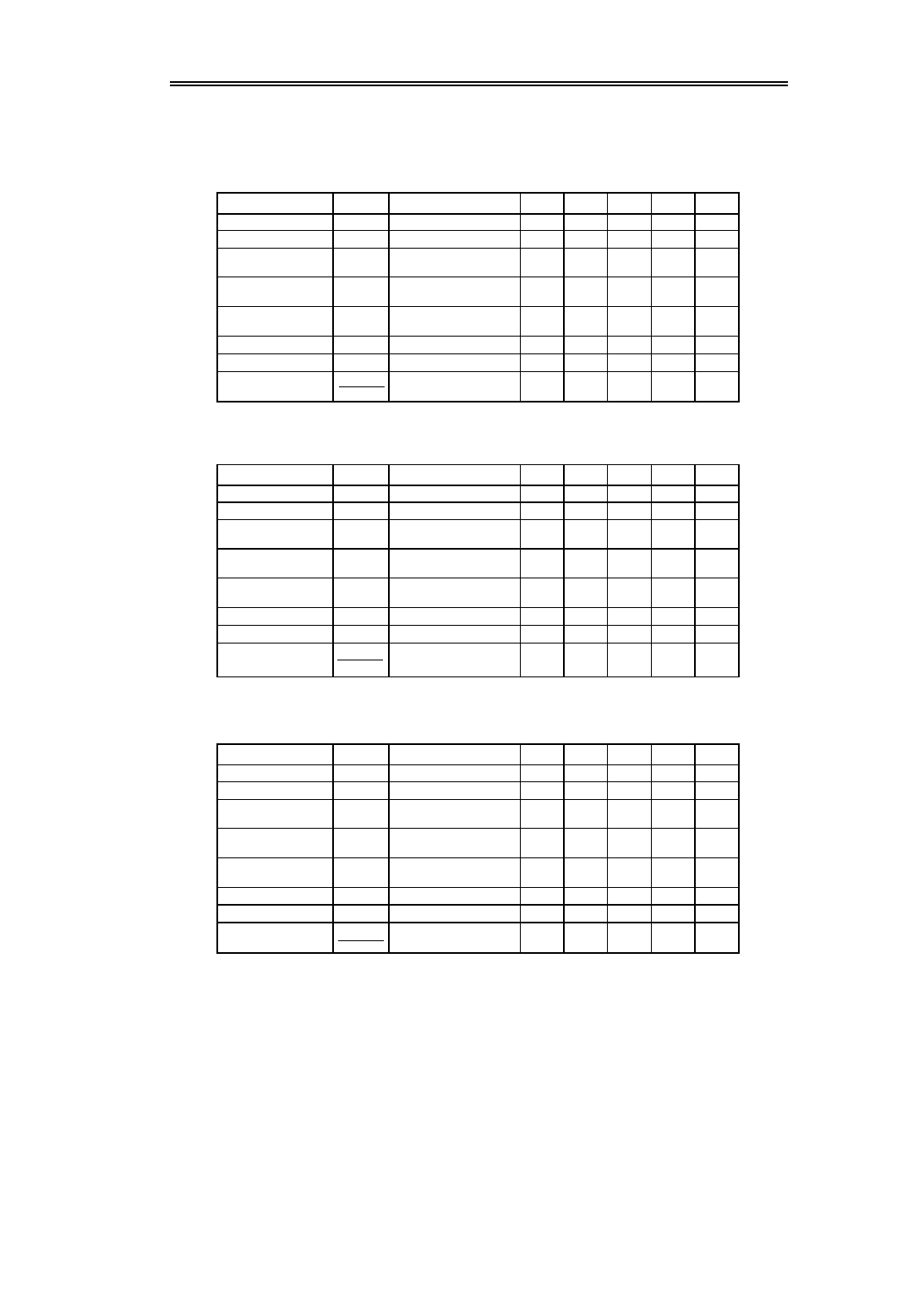
Electrical Characteristics
1.
S-81211SGY-X, S-81211SGUP-DQA-X, S-81211SG-QA-X (1.1-V output type)
Parameter
Symbol
Conditions
Min.
Typ.
Max.
Unit
Test cir.
Output voltage
V
OUT
V
IN
=1.5 V, I
OUT
=0.5 mA
1.073
1.100
1.127
V
1
I/O voltage difference
V
dif
I
OUT
=0.5 mA
0.05
0.2
V
1
Line regulation 1
V
OUT
1
V
IN
=1.5 to 10 V
I
OUT
=0.5 mA
10
50
mV
1
Line regulation 2
V
OUT
2
V
IN
=1.5 to 10 V
I
OUT
=10
A
10
77
mV
1
Load regulation
V
OUT
3
V
IN
=1.5 V
I
OUT
=10
A to 0.5 mA
10
100
mV
1
Current consumption
I
SS
V
IN
=1.5 V, Unloaded
1.2
2.5
A
2
Input voltage
V
IN
10
V
Temperature charac-
teristic of
V
OUT
V
OUT
Ta
V
IN
=1.5 V, I
OUT
= 0.5 mA
Ta=-40
C to 85
C
±0.138
mV/
C
2. S-81215SGY-X, S-81215SGUP-DQK-X, S-81215SG-QK-X (1.5-V output type)
Parameter
Symbol
Conditions
Min.
Typ.
Max.
Unit
Test cir.
Output voltage
V
OUT
V
IN
=3.5 V, I
OUT
=0.5 mA
1.464
1.500
1.536
V
1
I/O voltage difference
V
dif
I
OUT
=0.5 mA
0.03
0.18
V
1
Line regulation 1
V
OUT
1
V
IN
=2.5 to 10 V
I
OUT
=0.5 mA
7
39
mV
1
Line regulation 2
V
OUT
2
V
IN
=2.5 to 10 V
I
OUT
=1
A
7
105
mV
1
Load regulation
V
OUT
3
V
IN
=3.5 V
I
OUT
=1
A to10 mA
80
120
mV
1
Current consumption
I
SS
V
IN
=3.5 V, Unloaded
1.2
2.5
A
2
Input voltage
V
IN
10
V
Temperature charac-
teristic of
V
OUT
V
OUT
Ta
V
IN
=3.5 V, I
OUT
= 0.5 mA
Ta=-40
C to 85
C
±0.188
mV/
C
3. S-81217SG-QQ-X (1.7-V output type)
Parameter
Symbol
Conditions
Min.
Typ.
Max.
Unit
Test cir.
Output voltage
V
OUT
V
IN
=3.7 V, I
OUT
=10 mA
1.659
1.700
1.741
V
1
I/O voltage difference
V
dif
I
OUT
=10 mA
0.77
1.63
V
1
Line regulation 1
V
OUT
1
V
IN
=2.7 to 10 V
I
OUT
=1 mA
8
43
mV
1
Line regulation 2
V
OUT
2
V
IN
=2.7 to 10 V
I
OUT
=1
A
8
119
mV
1
Load regulation
V
OUT
3
V
IN
=3.7 V
I
OUT
=1
A to 10 mA
80
120
mV
1
Current consumption
I
SS
V
IN
=3.7 V, Unloaded
1.2
2.5
A
2
Input voltage
V
IN
10
V
Temperature charac-
teristic of
V
OUT
V
OUT
Ta
V
IN
=3.7 V, I
OUT
= 10 mA
Ta=-40
C to 85
C
±0.213
mV/
C
Table 3
(Unless otherwise specified: Ta=25
C)
Table 4
(Unless otherwise specified: Ta=25
C)
Table 5
(Unless otherwise specified: Ta=25
C)

HIGH PRECISION VOLTAGE REGULATOR
S-812XXSG Series
4
Seiko Instruments Inc.
4.
S-81218SG-QR-X (1.8-V output type)
Parameter
Symbol
Conditions
Min.
Typ.
Max.
Unit
Test cir.
Output voltage
V
OUT
V
IN
=3.8 V, I
OUT
=10 mA
1.756
1.800
1.843
V
1
I/O voltage difference
V
dif
I
OUT
=10 mA
0.72
1.55
V
1
Line regulation 1
V
OUT
1
V
IN
=2.8 to 10 V
I
OUT
=1 mA
8
45
mV
1
Line regulation 2
V
OUT
2
V
IN
=2.8 to 10 V
I
OUT
=1
A
8
126
mV
1
Load regulation
V
OUT
3
V
IN
=3.8 V
I
OUT
=1
A to 10 mA
80
120
mV
1
Current consumption
I
SS
V
IN
=3.8 V, Unloaded
1.2
2.5
A
2
Input voltage
V
IN
10
V
Temperature charac-
teristic of
V
OUT
V
OUT
Ta
V
IN
=3.8 V, I
OUT
= 10 mA
Ta=-40
C to 85
C
±0.225
mV/
C
5.
S-81220SGY-X, S-81220SGUP-DQS-X, S-81220SG-QS-X (2.0-V output type)
Parameter
Symbol
Conditions
Min.
Typ.
Max.
Unit
Test cir.
Output voltage
V
OUT
V
IN
=4.0 V, I
OUT
=10 mA
1.592
2.000
2.048
V
1
I/O voltage difference
V
dif
I
OUT
=10 mA
0.63
1.39
V
1
Line regulation 1
V
OUT
1
V
IN
=3.0 to 10 V
I
OUT
=1 mA
8
48
mV
1
Line regulation 2
V
OUT
2
V
IN
=3.0 to 10 V
I
OUT
=1
A
8
140
mV
1
Load regulation
V
OUT
3
V
IN
=4.0 V
I
OUT
=1
A to 10 mA
80
120
mV
1
Current consumption
I
SS
V
IN
=4.0 V, Unloaded
1.2
2.5
A
2
Input voltage
V
IN
10
V
Temperature charac-
teristic of
V
OUT
V
OUT
Ta
V
IN
=4.0 V, I
OUT
= 10 mA
Ta=-40
C to 85
C
±0.250
mV/
C
6.
S-81221SGUP-DQU-X (2.1-V output type)
Parameter
Symbol
Conditions
Min.
Typ.
Max.
Unit
Test cir.
Output voltage
V
OUT
V
IN
=4.1 V, I
OUT
=10 mA
2.049
2.100
2.151
V
1
I/O voltage difference
V
dif
I
OUT
=10 mA
0.59
1.32
V
1
Line regulation 1
V
OUT
1
V
IN
=3.1 to 10 V
I
OUT
=1 mA
9
50
mV
1
Line regulation 2
V
OUT
2
V
IN
=3.1 to 10 V
I
OUT
=1
A
9
147
mV
1
Load regulation
V
OUT
3
V
IN
=4.1 V
I
OUT
=1
A to 10 mA
80
120
mV
1
Current consumption
I
SS
V
IN
=4.1 V, Unloaded
1.2
2.5
A
2
Input voltage
V
IN
10
V
Temperature charac-
teristic of
V
OUT
V
OUT
Ta
V
IN
=4.1 V, I
OU
T = 10 mA
Ta=-40
C to 85
C
±0.263
mV/
C
Table 6
(Unless otherwise specified
:
Ta=25
C)
Table 7
(Unless otherwise specified
:
Ta=25
C)
Table 8
(Unless otherwise specified
:
Ta=25
C)