 | –≠–ª–µ–∫—Ç—Ä–æ–Ω–Ω—ã–π –∫–æ–º–ø–æ–Ω–µ–Ω—Ç: S-8130AC | –°–∫–∞—á–∞—Ç—å:  PDF PDF  ZIP ZIP |

Rev. 1.2
_00
Seiko Instruments Inc.
1
Temperature Switch with Latch
S-8130AC
The S-8130AC is a temperature switch with a latch function
having a built-in semiconductor temperature sensor. The output
signal is inverted when the temperature is detected, and latched
until a reset signal input or a detection of the power voltage
lowering.
Low voltage operation down to 2.2 V is possible and the current
consumption is low, 15
µA (typ.), due to CMOS configuration.
The S-8130AC consists of a temperature sensor having the
temperature coefficient of
-13 mV/∞C, a reference voltage source,
a comparator, voltage detection circuit, and noise suppression
circuit all of which is enclosed in a small 8-Pin MSOP package.
Available temperature range is between
-40 to +100 ∞C and wide
application in temperature control can be achieved since the output
linearity is excellent compared to other sensors including
thermistors.
Features
Applications
∑ V
SS
grounded temperature voltage output
∑ Game console
∑ Low voltage operation : V
DD
(min.)=2.2 V
∑ Electronic devices
∑ Low current consumption : 15 µA typ. (+25∞C)
∑ Noise suppression at temperature detection
∑ Detection temperature is determined with external resistance
∑ Output logic level is fixed by the latch after temperature detection
∑ Small plastic package : 8-Pin MSOP
Package
∑ 8-Pin MSOP (PKG drawing code : FN008-A)

Temparature Switch with Latch
Rev. 1.2
_00
S-8130AC
2
Seiko Instruments Inc.
Block diagram
S-8130ACXFN-XXX-T2 (Built-in temperature sensor and external setting for detection temperature)
VDD
VSS
Temparature
Sensor
D
CK
D-F/F
CD1
CD2
RESET
Reference
voltage source
Voltage detector
with delay circuit
DET
+
-
Vref
VOUT
RT
Vref
R
Q
Figure 1
Selection Guide
Product name
S - 8130 A C X F N - X X X - T 2
Taping direction (Direction of IC in tape)
Abbreviated Code
Option code
Option list
∑ DET output should be high-active or low-active.
∑ Release voltage V
RET
can be selected 0.1 V step in the range between 2.2 and 3.4 V.
∑ RESET pin should be selected from PuII-up or Nch Open Drain.
Product name
DET output
V
RET
RESET
S-8130ACAFN-MAC-T2
High-active
2.4 V
Pull-up
When other combination is required, please ask our sales office.
Rev. 1.2
_00
Temperature Switch with Latch
S-8130AC
Seiko Instruments Inc.
3
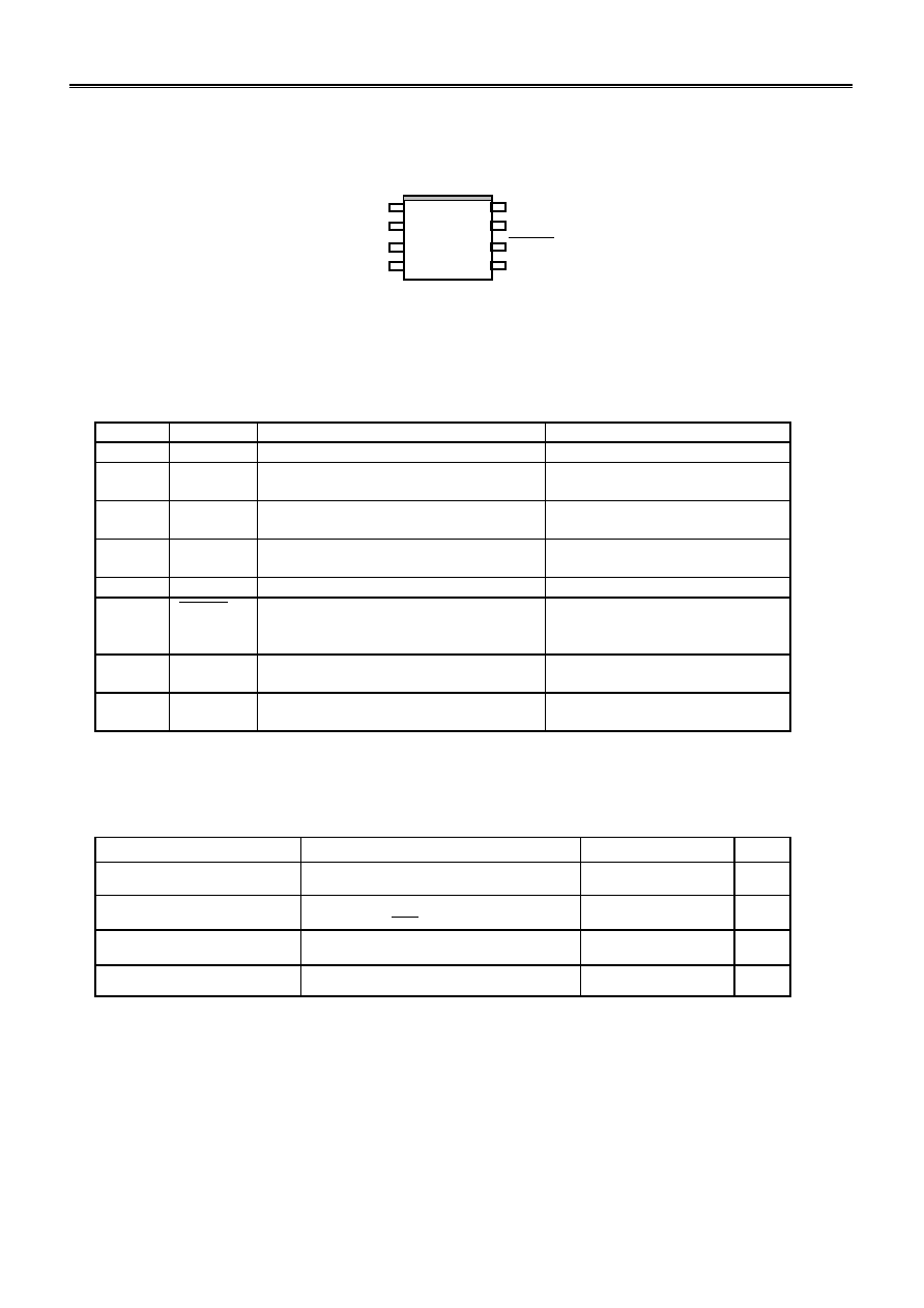
Pin configuration
8-Pin MSOP
Top view
1
2
3
4
8
7
6
5
VDD
DET
CD2
CD1
VOUT
RT
VSS
RESET
Figure
2
Pin Description
Pin No.
Pin Name
Function
Input/Output
1
VDD
Positive power supply pin
2
DET
Output pin for detection at the defined
temperature
CMOS output : Output logic is
selectable
3
CD2
Capacitor connection pin for delay time
setting in voltage detection
Input/Output
4
CD1
Capacitor connection pin for noise
filtering time
Input/Output
5 VSS Ground
pin
6
RESET
Input/Output pin for reset
Low-active
Input : CMOS
Output : N channel open drain
(Pull-up resistance is optional)
7
RT
Reference voltage input pin (short-
circuited to VOUT pin internally)
Input
8
VOUT
Output pin for reference voltage from
the internal comparator
Output
Absolute maximum ratings
(Ta = 25
∞C unless otherwise specified)
Parameter Symbol
Ratings
Unit
Supply voltage (V
SS
=0.0 V)
V
DD
V
SS
+12
V
Pin voltage
V
OUT
, V
RT
, V
RESET
, V
DET
, V
CD1
, V
CD2
V
SS
-0.3 to V
DD
+0.3
V
Operating temperature
T
opr
-40 to +100
∞C
Storage temperature
T
stg
-55 to +125
∞C
Caution The absolute maximum ratings are rated values exceeding which the product could suffer
physical damage. These values must therefore not be exceeded under any conditions.
Temparature Switch with Latch
Rev. 1.2
_00
S-8130AC
4
Seiko Instruments Inc.
Recommended values for external parts
Parameters Symbol Value Unit
CD1 capacitance
C
D1
4.7 nF
CD2 capacitance
C
D2
4.7 nF
Resistance between VOUT and RT
R
1
According to setting detection
temperature
k
Resistance between RT and VSS
R
2
According to setting detection
temperature
k
DC Electrical Characteristics
(Ta=25∞C, V
SS
=0 V unless otherwise specified)
Parameters Symbol
Conditions
Min.
Typ.
Max.
Unit
Supply voltage
V
DD
2.2
10.0 V
Output current 1
I
DETH
V
DD
=3 V
Applied to
V
DET
=2.2 V
2
4
mA
I
DETL
DET
pin V
DET
=0.4 V
0.5
1
mA
Input voltage
V
ONH
Applied to RESET pin
0.8
◊ V
DD
V
DD
V
V
ONL
V
SS
0.2
◊ V
DD
V
Pull-up resistance
R
OL
Applied to RESET pin
V
IN
=0 V, V
DD
=3.0 V
30 100 300
k
Sensor voltage
V
SENSOR
Ta=
+60∞C
1.562
V
Ta=
+100∞C
1.029
V
Release voltage for
voltage detector
V
R
V
RET
◊
0.98
V
RET
V
RET
◊
1.02
V
Hysteresis width for
voltage detector
V
HYS
V
RET
◊
0.05
V
Output current for
voltage detector
I
RSTL
V
DD
=3.0 V, V
RESET
=0.5 V
Applied to
RESET
pin
0.5
1
mA
Temperature
coefficient for
voltage detector
V
Ta V
RET
RET
∑
Ta=
-40 to 100∞C
±100
ppm/
∞C
Output voltage
V
VO
V
DD
=3.0 V, I
OUT
=1.0 mA
Applied to VOUT pin (when
the external reference voltage
is used)
1.960 2.000 2.040 V
Output current 2
I
VO
V
DD
=2.6 V, Applied to VOUT
pin (when the external
reference voltage is used)
1.0
*1
mA
Operating current
I
DD
V
DD
=3.3 V
15 30
µA
*1. Output current can be drawn to this value. Current which exceeds this value should not be provided to the
load.

Rev. 1.2
_00
Temperature Switch with Latch
S-8130AC
Seiko Instruments Inc.
5
AC Electrical Characteristics
(Ta=25∞C unless otherwise specified)
Parameters Symbol Conditions
Min. Typ. Max. Unit
Noise filtering time
T
noise
C
D1
=4.7 nF, V
DD
=3 V
10
30
50
ms
Delay time for
voltage detector
T
delay
C
D2
=4.7 nF, V
DD
=3 V
10
30
50
ms
Definition of the symbols used in the voltage detection circuit
A
B
V
DD
T
delay
V
SS
Release voltage (V
RET
)
Detection voltage
Minimum operating voltage
RESETpin voltage (V
DD
)
Hysteresis width
(V
HYS
)
V
SS
Figure
3
Description of Operation
1. Basic operation
S-8130AC series is a temperature switch which detects a certain temperature and sends a signal to an
external device. Combination of the parameters such as release voltage and DET output logic can be selected.
In the following DET output is supposed to be high-active.
When the power voltage is turned on, the DET pin voltage goes to "L" since the flip-flop circuit in the
detection circuit is cleared by the delayed voltage detection circuit. Temperature detection then starts and the
DET pin is held "L" as long as the temperature is lower than the detection temperature. The temperature goes
high and exceeds the detection temperature for longer than the time defined by the capacitor connected to the
CD1 pin, then the DET pin goes to "H". Once the over-temperature is detected and the DET pin goes to "H", the
state is held by the flip-flop circuit. In order to release the state the
RESET
pin voltage should be set to "L" by the
external signal or the power voltage should be set under the detection voltage of the built-in detector to reset the
internal circuit.
Note : The detection temperature can be set arbitrarily by connecting resistances between VOUT pin and RT
pin, and between RT pin and VSS pin since the divided voltage is applied to the internal comparator as
the reference voltage. Sufficient evaluation is needed to choose resistance values since the detection
temperature is determined by the resistance temperature coefficient, IC characteristics, etc. Current
which flows through these resistances should be less than 1 mA.
Noise filtering circuit
The noise filtering circuit prevents malfunction of the temperature switch caused by noise.
The noise filtering circuit starts charging of the capacitor connected to the CD1 pin when the output of the
internal comparator enters active state due to an external noise or a rapid change in the power voltage. In
the normal operation the flip-flop circuit is set when the capacitor is charged to a certain voltage. But in the
noise triggered operation the comparator output goes back to inactive state and the CD1 pin voltage is held
low since the charging of the capacitor is insufficient. As a result the DET pin is held low and malfunction
does not occur.

Temparature Switch with Latch
Rev. 1.2
_00
S-8130AC
6
Seiko Instruments Inc.
Noise filtering time, T
noise
, is determined by the time constant consisting of internal constant current and the
capacitance C
D1
, and calculated by the following equation.
T
noise
(ms)=Noise fitering time coefficient
◊ C
D1
(nF)
Noise fitering time coefficient (25∞C): Typ. 6.4
2. Voltage detection circuit with delay
The delay circuit of the voltage detector provides a delayed output signal to the RESET pin when the power
voltage V
DD
rises and exceeds the release voltage V
R
.
On the other hand no delay occurs when the power
voltage V
DD
goes lower than the detection voltage, V
R
-V
HYS
.
The delay time, T
delay
, is determined by the time constant consisting of internal constant current and the
capacitance C
D2
, and calculated by the following equation.
T
delay
(ms)=Delay coefficient
◊ C
D2
(nF)
Delay coefficient (25∞C): Min. 4.3, Typ. 6.4, Max. 8.5
∑ When the board wiring is made, attention should be paid that no current flows into or flows out of the
CD2 pin to have correct delay time since the impedance of the CD2 pin is high.
∑ Capacitance of the external capacitor C
D2
has no limitation as long as its leak current is negligible
compared to the internal constant current. Error in delay time occurs If the capacitor has leak current.
When the leak current is larger than the internal constant current, no release takes place.
Application circuit
Protection
circuit
VSS
CD1
VDD
RT
DET
CD2
S-8130AC
RESET
VOUT
C P U
VSS
Output port
(Input port)
VDD
Figure 4
Caution The above connection diagram will not guarantee successful operation.
Precautions
(1) Since the S-8130AC has a voltage detector inside, control for the
RESET
pin is not necessary to activate
the circuit unlike the Figure 4. In this case the
RESET
pin should be open.
(2) Current which is provided to the resistances from the VOUT pin should be less than 1 mA.
(3) A capacitor of around 1
µF should be connected to the DET pin to prevent malfunction caused by a noise
due to the power on.
(4) Do not apply an electrostatic discharge to this IC that exceeds the performance ratings of the built-in
electrostatic protection circuit.

Rev. 1.2
_00
Temperature Switch with Latch
S-8130AC
Seiko Instruments Inc.
7
Typical Characteristics
1. Current consumption vs. power voltage
2. Reference voltage vs. Power voltage
0
1
2
3
4
5
6
7
8
9
10
V
DD
(V)
Ta=-40∞C
100∞C
25∞C
I
DD
V
DD
V
SS
=0V
I
DD
(
µA)
10.0
11.0
12.0
13.0
14.0
1.96
1.97
1.98
1.99
2.00
2.01
2.02
2.03
2.04
0
1
2
3
4
5
6
7
8
9
10
V
DD
(V)
V
VO
(V)
Ta=100∞C
25∞C
-40∞C
V
OUT
V
DD
V
SS
=0V
3. Temperature sensor output vs. temperature
0.0
0.5
1.0
1.5
2.0
2.5
3.0
-40
-20
0
20
40
60
80
100
Temp(∞C)
Vsensor
(V)
Vsenser
V
DD
V
SS
=0V
4. DET pin I
SOURCE
-V
DD
characteristics
5. DET pin I
SINK
-V
DD
characteristics
0
2
4
6
8
10
0
1
2
3
4
5
6
7
8
9
10
V
DD
I
SOURCE
(mA)
(V)
100∞C
Ta=-40∞C
25∞C
I
SOURCE
V
DD
VOH=V
DD
- 0.8V
0
5
10
15
20
25
0
1
2
3
4
5
6
7
8
9
10
V
DD
I
SINK
(mA)
(V)
Ta=-40∞C
100∞C
25∞C
I
SINK
V
DD
VOL=0.4V
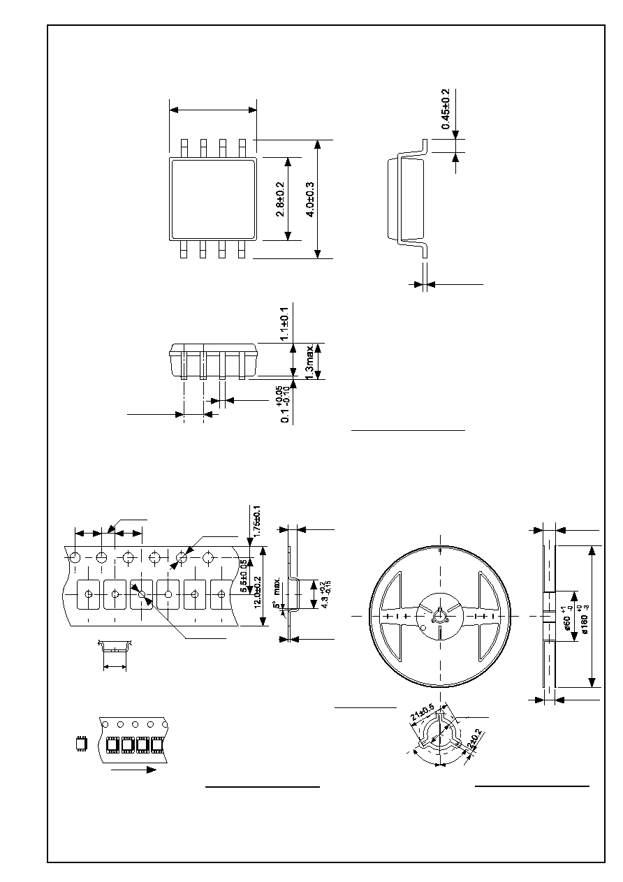
l Reel Specifications
l Tape Specifications
l Dimensions
n 8-Pin MSOP
FN008-A
Rev.1.0
020213
2.95±0.2
8
5
0.2±0.1
0.65±0.1
0.13±0.1
1
4
No. : FN008-A-P-SD-1.0
T2(TB)
0.3±0.05
1.35±0.15
1.05±0.05
1.55±0.05
2.0±0.05
4.0±0.1
3.1±0.15
4.0±0.1
1
4
5 8
Feed direction
No. : FN008-A-C-SD-1.0
(60∞)
(60∞)
13±0.2
16.5max.
13.0±0.3
Winding core
No. : FN008-A-R-SD-1.0
3000 pcs/reel

∑
The information described herein is subject to change without notice.
∑
Seiko Instruments Inc. is not responsible for any problems caused by circuits or diagrams described herein
whose related industrial properties, patents, or other rights belong to third parties. The application circuit
examples explain typical applications of the products, and do not guarantee the success of any specific
mass-production design.
∑
When the products described herein are regulated products subject to the Wassenaar Arrangement or other
agreements, they may not be exported without authorization from the appropriate governmental authority.
∑
Use of the information described herein for other purposes and/or reproduction or copying without the
express permission of Seiko Instruments Inc. is strictly prohibited.
∑
The products described herein cannot be used as part of any device or equipment affecting the human
body, such as exercise equipment, medical equipment, security systems, gas equipment, or any apparatus
installed in airplanes and other vehicles, without prior written permission of Seiko Instruments Inc.
∑
Although Seiko Instruments Inc. exerts the greatest possible effort to ensure high quality and reliability, the
failure or malfunction of semiconductor products may occur. The user of these products should therefore
give thorough consideration to safety design, including redundancy, fire-prevention measures, and
malfunction prevention, to prevent any accidents, fires, or community damage that may ensue.