Document Outline
- S-814 Series
- Cover
- Features
- Applications
- Packages
- Block Diagrams
- Product Code Structure
- Pin Configurations
- Absolute Maximum Ratings
- Electrical Characteristics
- Test Circuits
- Standard Circuit
- Technical Terms
- Operation
- Selection of Output Capacitor (CL)
- Precautions
- Characteristics (Typical data)
- Transient Response Characteristics
- Package drawings
- SOT-23-5
- SOT-89-3
- SOT-89-5

Rev.1.5
_00
LOW DROPOUT CMOS VOLTAGE REGULATOR
S-814 Series
Seiko Instruments Inc.
1
The S-814 Series is a low dropout voltage, high output
voltage accuracy and low current consumption positive
voltage regulator developed utilizing CMOS technology.
Built-in low ON-resistance transistors provide low dropout
voltage and large output current. A shutdown circuit ensures
long battery life.
Various types of output capacitors can be used in the S-814
Series compared with the past CMOS voltage regulators.
(i.e., Small ceramic capacitors can also be used in the S-814
Series.)
The SOT-23-5 miniaturized package and the SOT-89-3 and
the SOT-89-5 packages are recommended to use for
configuring portable devices and large output current
applications, respectively.
Features
∑ Low current consumption
At operation mode:
Typ. 30
µA, Max. 40 µA
At shutdown mode:
Typ. 100 nA, Max. 500 nA
∑ Output voltage:
0.1 V steps between 2.0 and 6.0 V
∑ High accuracy output voltage:
±2.0 %
∑ Output current:
110 mA capable: 3.0 V output product, at V
IN
=4 V
*1
180 mA capable: 5.0 V output product, at V
IN
=6 V
*1
∑ Low dropout voltage:
Typ. 170 mV:
5.0 V output product, at I
OUT
=60 mA
∑ Built-in shutdown circuit
Selection without a shutdown function is possible. (S-814AxxAUA
Series)
∑ Built-in short-circuit protection
∑ Low ESR capacitor, e.g. a ceramic capacitor of 0.47 µF or more, can be used as the output capacitor.
∑ Small package:
SOT-23-5, SOT-89-3, and SOT-89-5
*1. Attention should be paid to the power dissipation of the package when the output current is large.
Applications
∑ Power source for battery-powered devices, personal communication devices, and home electric/electronic
appliances.
Packages
∑ SOT-23-5 (Package drawing code: MP005-A)
∑ SOT-89-3 (Package drawing code: UP003-A)
∑ SOT-89-5 (Package drawing code: UP005-A)
LOW DROPOUT CMOS VOLTAGE REGULATOR
Rev.1.5
_00
S-814 Series
2
Seiko Instruments Inc.
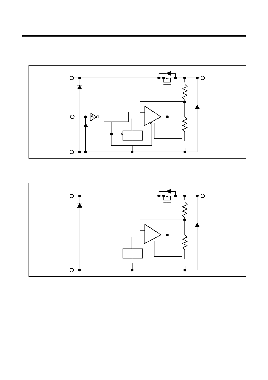
Block Diagrams
1. S-814xxxAMC Series, S-814xxxAUC Series
VOUT
ON/OFF
VSS
VIN
+
-
*1
Short-circuit
protection
circuit
Shutdown
circuit
Reference
voltage
*1. Parasitic diode
Figure 1
2. S-814AxxAUA Series
VOUT
VSS
VIN
+
-
*1
Short-circuit
protection
circuit
Reference
voltage
*1. Parasitic diode
Figure 2
Rev.1.5
_00
LOW DROPOUT CMOS VOLTAGE REGULATOR
S-814 Series
Seiko Instruments Inc.
3
Product Code Structure
1. Product name
S-814 x xx A xx- xxx- T2
IC direction in tape specifications
*1
Product name (Abbreviation)
*2
Package name (Abbreviation)
MC: SOT-23-5
UA: SOT-89-3
UC: SOT-89-5
Output voltage
20 to 60
(E.g., When output voltage is 2.0 V, it is expressed as 20.)
Product type
*3
A:
OFF
/
ON
pin positive logic (SOT-23-5, SOT-89-5),
or without shutdown function (SOT-89-3)
B:
OFF
/
ON
pin negative logic
*1. Refer to the taping specifications at the end of this book.
*2. Refer to the Table 1 in "2. Product name list".
*3. Refer to "3. ON/OFF pin (Shutdown pin)" in " Operation".
Remark A ON/OFF pin and a shutdown circuit are not in S-814AxxAUA Series.
2. Product name list
Table1 (1/2)
Output
voltage
SOT-23-5 SOT-89-3 SOT-89-5
2.0 V
±2.0 %
S-814A20AMC-BCK-T2
S-814A20AUC-BCK-T2
2.1 V
±2.0 %
S-814A21AMC-BCL-T2
S-814A21AUC-BCL-T2
2.2 V
±2.0 %
S-814A22AMC-BCM-T2
S-814A22AUC-BCM-T2
2.3 V
±2.0 %
S-814A23AMC-BCN-T2
S-814A23AUC-BCN-T2
2.4 V
±2.0 %
S-814A24AMC-BCO-T2
S-814A24AUC-BCO-T2
2.5 V
±2.0 %
S-814A25AMC-BCP-T2
S-814A25AUC-BCP-T2
2.6 V
±2.0 %
S-814A26AMC-BCQ-T2
S-814A26AUC-BCQ-T2
2.7 V
±2.0 %
S-814A27AMC-BCR-T2
S-814A27AUC-BCR-T2
2.8 V
±2.0 %
S-814A28AMC-BCS-T2
S-814A28AUC-BCS-T2
2.9 V
±2.0 %
S-814A29AMC-BCT-T2
S-814A29AUC-BCT-T2
3.0 V
±2.0 %
S-814A30AMC-BCU-T2 S-814A30AUA-BCU-T2 S-814A30AUC-BCU-T2
3.1 V
±2.0 %
S-814A31AMC-BCV-T2
S-814A31AUC-BCV-T2
3.2 V
±2.0 %
S-814A32AMC-BCW-T2
S-814A32AUC-BCW-T2
3.3 V
±2.0 %
S-814A33AMC-BCX-T2 S-814A33AUA-BCX-T2 S-814A33AUC-BCX-T2
3.4 V
±2.0 %
S-814A34AMC-BCY-T2
S-814A34AUC-BCY-T2
3.5 V
±2.0 %
S-814A35AMC-BCZ-T2
S-814A35AUC-BCZ-T2
3.6 V
±2.0 %
S-814A36AMC-BDA-T2
S-814A36AUC-BDA-T2
3.7 V
±2.0 %
S-814A37AMC-BDB-T2
S-814A37AUC-BDB-T2
3.8 V
±2.0 %
S-814A38AMC-BDC-T2
S-814A38AUC-BDC-T2
3.9 V
±2.0 %
S-814A39AMC-BDD-T2
S-814A39AUC-BDD-T2

LOW DROPOUT CMOS VOLTAGE REGULATOR
Rev.1.5
_00
S-814 Series
4
Seiko Instruments Inc.
Table 1 (2/2)
Output
voltage
SOT-23-5 SOT-89-3 SOT-89-5
4.0 V
±2.0 %
S-814A40AMC-BDE-T2
S-814A40AUC-BDE-T2
4.1 V
±2.0 %
S-814A41AMC-BDF-T2
S-814A41AUC-BDF-T2
4.2 V
±2.0 %
S-814A42AMC-BDG-T2
S-814A42AUC-BDG-T2
4.3 V
±2.0 %
S-814A43AMC-BDH-T2
S-814A43AUC-BDH-T2
4.4 V
±2.0 %
S-814A44AMC-BDI-T2
S-814A44AUC-BDI-T2
4.5 V
±2.0 %
S-814A45AMC-BDJ-T2
S-814A45AUC-BDJ-T2
4.6 V
±2.0 %
S-814A46AMC-BDK-T2
S-814A46AUC-BDK-T2
4.7 V
±2.0 %
S-814A47AMC-BDL-T2
S-814A47AUC-BDL-T2
4.8 V
±2.0 %
S-814A48AMC-BDM-T2
S-814A48AUC-BDM-T2
4.9 V
±2.0 %
S-814A49AMC-BDN-T2
S-814A49AUC-BDN-T2
5.0 V
±2.0 %
S-814A50AMC-BDO-T2
S-814A50AUC-BDO-T2
5.1 V
±2.0 %
S-814A51AMC-BDP-T2
S-814A51AUC-BDP-T2
5.2 V
±2.0 %
S-814A52AMC-BDQ-T2
S-814A52AUC-BDQ-T2
5.3 V
±2.0 %
S-814A53AMC-BDR-T2
S-814A53AUC-BDR-T2
5.4 V
±2.0 %
S-814A54AMC-BDS-T2
S-814A54AUC-BDS-T2
5.5 V
±2.0 %
S-814A55AMC-BDT-T2
S-814A55AUC-BDT-T2
5.6 V
±2.0 %
S-814A56AMC-BDU-T2
S-814A56AUC-BDU-T2
5.7 V
±2.0 %
S-814A57AMC-BDV-T2
S-814A57AUC-BDV-T2
5.8 V
±2.0 %
S-814A58AMC-BDW-T2
S-814A58AUC-BDW-T2
5.9 V
±2.0 %
S-814A59AMC-BDX-T2
S-814A59AUC-BDX-T2
6.0 V
±2.0 %
S-814A60AMC-BDY-T2
S-814A60AUC-BDY-T2
Remark Contact our sales person for products with an output voltage other than those specified above or
product type B.

Rev.1.5
_00
LOW DROPOUT CMOS VOLTAGE REGULATOR
S-814 Series
Seiko Instruments Inc.
5
Pin Configurations
Table 2
Pin No.
Symbol
Pin description
1
VIN
Voltage input pin
2
VSS
GND
pin
3
ON/OFF
Shutdown
pin
4
NC
*1
No connection
5
VOUT
Voltage output pin
SOT-23-5
Top view
5
4
3
2
1
*1. The NC pin is electrically open.
The NC pin can be connected to VIN or VSS.
Figure 3
Table 3
Pin No.
Symbol
Pin description
1
VOUT
Voltage output pin
2
VSS
GND
pin
3
VIN
Voltage input pin
SOT-89-3
Top view
3
2
1
Figure 4
Table 4
Pin No.
Symbol
Pin description
1
VOUT
Voltage output pin
2
VSS
GND
pin
3
NC
*1
No connection
4
ON/OFF
Shutdown
pin
5
VIN
Voltage input pin
SOT-89-5
Top view
1
3
2
4
5
*1. The NC pin is electrically open.
The NC pin can be connected to VIN or VSS.
Figure 5

LOW DROPOUT CMOS VOLTAGE REGULATOR
Rev.1.5
_00
S-814 Series
6
Seiko Instruments Inc.
Absolute Maximum Ratings
Table 5
(Ta
=25∞C unless otherwise specified)
Item
Symbol
Absolute maximum rating
Unit
Input voltage
V
IN
V
SS
-0.3 to V
SS
+12
V
V
ON/OFF
V
SS
-0.3 to V
SS
+12
Output voltage
V
OUT
V
SS
-0.3 to V
IN
+0.3
Power dissipation
P
D
SOT-23-5 250
mW
SOT-89-3
500
SOT-89-5
500
Operating ambient temperature
Topr
-40 to +85
∞C
Storage ambient temperature
Tstg
-40 to +125
Caution The absolute maximum ratings are rated values exceeding which the product could suffer
physical damage. These values must therefore not be exceeded under any conditions.
Rev.1.5
_00
LOW DROPOUT CMOS VOLTAGE REGULATOR
S-814 Series
Seiko Instruments Inc.
7
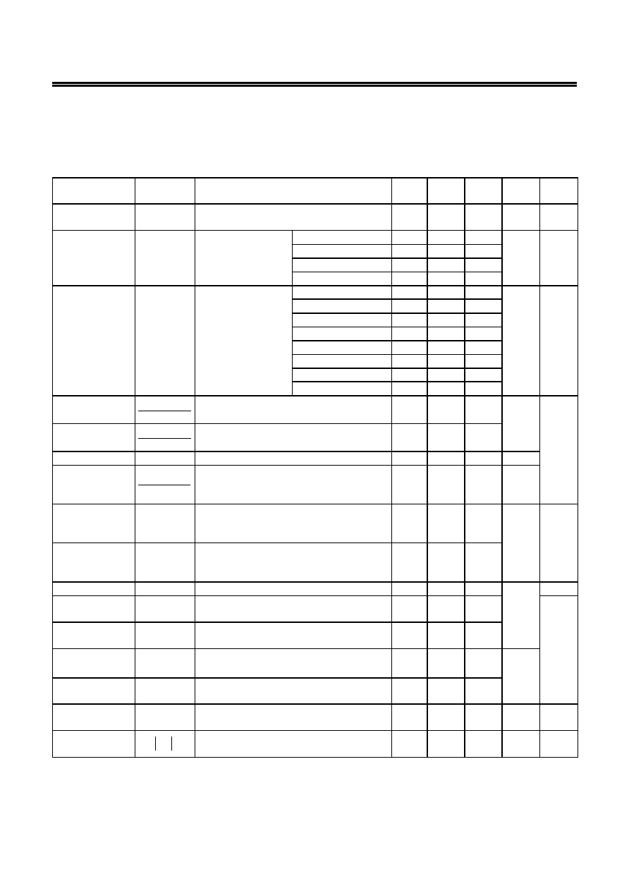
Electrical Characteristics
1. S-814xxxAMC Series, S-814AxxAUC Series
Table 6
(Ta
=25∞C unless otherwise specified)
Item Symbol
Conditions
Min.
Typ.
Max.
Units
Test
circuit
Output voltage
*1
V
OUT(E)
V
IN
=V
OUT(S)
+1 V, I
OUT
=30 mA
V
OUT(S)
◊0.98
V
OUT(S)
V
OUT(S)
◊1.02
V 1
Output current
*2
I
OUT
V
OUT(S)
+1 VV
IN
10 V 2.0 VV
OUT(S)
2.9 V
100
*3
mA 3
3.0 V
V
OUT(S)
3.9 V
110
*3
4.0 V
V
OUT(S)
4.9 V
135
*3
5.0 V
V
OUT(S)
6.0 V
180
*3
Dropout voltage
*4
V
drop
I
OUT
=60 mA
2.0 V
V
OUT(S)
2.4 V
0.51 0.87 V
1
2.5 V
V
OUT(S)
2.9 V
0.38 0.61
3.0 V
V
OUT(S)
3.4 V
0.30 0.44
3.5 V
V
OUT(S)
3.9 V
0.24 0.33
4.0 V
V
OUT(S)
4.4 V
0.20 0.26
4.5 V
V
OUT(S)
4.9 V
0.18 0.22
5.0 V
V
OUT(S)
5.4 V
0.17 0.21
5.5 V
V
OUT(S)
6.0 V
0.17 0.20
Line regulation 1
OUT
IN
1
OUT
V
V
V
∑
V
OUT(S)
+0.5 VV
IN
10 V, I
OUT
=30 mA
0.05 0.2 %/V 1
Line regulation 2
OUT
IN
2
OUT
V
V
V
∑
V
OUT(S)
+0.5 VV
IN
10 V, I
OUT
=10 µA
0.05 0.2
Load regulation
V
OUT3
V
IN
=V
OUT(S)
+1 V, 10 µAI
OUT
80 mA
30 50 mV
Output voltage
temperature
cofficient
*5
OUT
OUT
V
Ta
V
∑
V
IN
=V
OUT(S)
+1 V, I
OUT
=30 mA,
-40∞CTa85∞C
±100
ppm/
∞C
Current
consumption
during operation
I
SS1
V
IN
=V
OUT(S)
+1 V, ON/OFF pin=ON, No load
30 40
µA
2
Current
consumption
during shutdown
I
SS2
V
IN
=V
OUT(S)
+1 V, ON/OFF pin
=OFF, No load
0.1 0.5
Input voltage
V
IN
10 V 1
ON/OFF pin
input voltage "H"
V
SH
V
IN
=V
OUT(S)
+1 V, R
L
=1 k,
Judged at V
OUT
level
1.5
4
ON/OFF pin
input voltage
"L"
V
SL
V
IN
=V
OUT(S)
+1 V, R
L
=1 k,
Judged at V
OUT
level
0.3
ON/OFF pin
input current "H"
"
I
SH
V
IN
=V
OUT(S)
+1 V, V
ON/OFF
=7 V
-0.1
0.1
µA
ON/OFF pin
input current
"L"
I
SL
V
IN
=V
OUT(S)
+1 V, V
ON/OFF
=0 V
-0.1
0.1
Short current
limit
I
OS
V
IN
=V
OUT(S)
+1 V, VOUT pin=0 V
70
mA 3
Ripple rejection
RR
V
IN
=V
OUT(S)
+1 V, f=100 Hz, Vrip=0.5 Vrms,
I
OUT
=30 mA
45
dB 5
*1. V
OUT(E)
: Specified output voltage
i.e., The output voltage when fixing I
OUT
(
=30 mA) and inputting V
OUT(S)
+1.0 V.
V
OUT(S)
: Effective output voltage
*2. Output amperage when output voltage goes below 95 % of V
OUT(E)
after gradually increasing output current.
*3. Use load amperage not exceeding this value.

LOW DROPOUT CMOS VOLTAGE REGULATOR
Rev.1.5
_00
S-814 Series
8
Seiko Instruments Inc.
*4. V
drop
=V
IN1
*1
-(V
OUT(E)
◊0.98)
*1. Input voltage at which the output voltage falls 98 % of V
OUT(E)
after gradually decreasing the input
voltage.
*5. The change in temperature [mV/∞C] is calculated using the following equation.
[
]
[ ]
[
]
1000
C
/
ppm
V
Ta
V
V
V
C
/
mV
Ta
V
OUT
OUT
)
S
(
OUT
OUT
˜
∞
∑
◊
=
∞
3
*
2
*
*1
*1. Change in temperature of the dropout voltage
*2. Specified output voltage
*3. Output voltage temperature coefficient
Rev.1.5
_00
LOW DROPOUT CMOS VOLTAGE REGULATOR
S-814 Series
Seiko Instruments Inc.
9
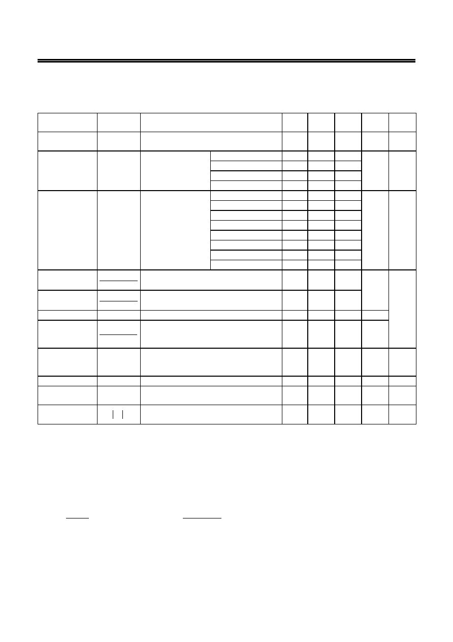
2. S-814AxxUA Series
Table 7
(Ta
=25∞C unless otherwise specified)
Item Symbol
Conditions
Min.
Typ.
Max.
Units
Test
circuit
Output voltage
*1
V
OUT(E)
V
IN
=V
OUT(S)
+1 V, I
OUT
=30 mA
V
OUT(S)
◊0.98
V
OUT(S)
V
OUT(S)
◊1.02
V 1
Output current
*2
I
OUT
V
OUT(S)
+1 VV
IN
10 V 2.0 VV
OUT(S)
2.9 V
100
*3
mA 3
3.0 V
V
OUT(S)
3.9 V
110
*3
4.0 V
V
OUT(S)
4.9 V
135
*3
5.0 V
V
OUT(S)
6.0 V
180
*3
Dropout voltage
*4
V
drop
I
OUT
=60 mA
2.0 V
V
OUT(S)
2.4 V
0.51 0.87 V
1
2.5 V
V
OUT(S)
2.9 V
0.38 0.61
3.0 V
V
OUT(S)
3.4 V
0.30 0.44
3.5 V
V
OUT(S)
3.9 V
0.24 0.33
4.0 V
V
OUT(S)
4.4 V
0.20 0.26
4.5 V
V
OUT(S)
4.9 V
0.18 0.22
5.0 V
V
OUT(S)
5.4 V
0.17 0.21
5.5 V
V
OUT(S)
6.0 V
0.17 0.20
Line regulation 1
OUT
IN
1
OUT
V
V
V
∑
V
OUT(S)
+0.5 VV
IN
10 V, I
OUT
=30 mA
0.05 0.2 %/V 1
Line regulation 2
OUT
IN
2
OUT
V
V
V
∑
V
OUT(S)
+0.5 VV
IN
10 V, I
OUT
=10 µA
0.05 0.2
Load regulation
V
OUT3
V
IN
=V
OUT(S)
+1 V, 10 µAI
OUT
80 mA
30 50 mV
Output voltage
temperature
cofficient
*5
OUT
OUT
V
Ta
V
∑
V
IN
=V
OUT(S)
+1 V, I
OUT
=30 mA,
-40∞CTa85∞C
±100
ppm/
∞C
Current
consumption
during operation
I
SS1
V
IN
=V
OUT(S)
+1 V, ON/OFF pin=ON, No load
30 40
µA
2
Input voltage
V
IN
10 V 1
Short current
limit
I
OS
V
IN
=V
OUT(S)
+1 V, VOUT pin=0 V
70
mA 3
Ripple rejection
RR
V
IN
=V
OUT(S)
+1 V, f=100 Hz, Vrip=0.5 Vrms,
I
OUT
=30 mA
45
dB 5
*1. V
OUT(E)
: Specified output voltage
i.e., The output voltage when fixing I
OUT
(
=30 mA) and inputting V
OUT(S)
+1.0 V.
V
OUT(S)
: Effective output voltage
*2. Output amperage when output voltage goes below 95 % of V
OUT(E)
after gradually increasing output current.
*3. Use load amperage not exceeding this value.
*4. V
drop
=V
IN1
*1
-(V
OUT(E)
◊0.98)
*1. Input voltage at which the output voltage falls 98 % of V
OUT(E)
after gradually decreasing the input
voltage.
*5. The change in temperature [mV/∞C] is calculated using the following equation.
[
]
[ ]
[
]
1000
C
/
ppm
V
Ta
V
V
V
C
/
mV
Ta
V
OUT
OUT
)
S
(
OUT
OUT
˜
∞
∑
◊
=
∞
3
*
2
*
*1
*1. Change in temperature of the dropout voltage
*2. Specified output voltage
*3. Output voltage temperature coefficient
LOW DROPOUT CMOS VOLTAGE REGULATOR
Rev.1.5
_00
S-814 Series
10
Seiko Instruments Inc.
Test Circuits
1.
VSS
VOUT
VIN
V
A
ON/OFF
*1
Set to power
ON
+
+
2.
VSS
VOUT
VIN
A
ON/OFF
*1
Set to
V
IN
or GND
Figure 6
Figure 7
3.
VSS
VOUT
VIN
V
A
ON/OFF
*1
Set to power
ON
+
+
4.
VSS
VOUT
VIN
V
R
L
ON/OFF
*1
A
+
Figure 8
Figure 9
5.
VSS
VOUT
VIN
V
ON/OFF
*1
Set to
power ON
R
L
+
Figure 10
*1. ON/OFF pin is not in the S-814AxxAUA Series.
Rev.1.5
_00
LOW DROPOUT CMOS VOLTAGE REGULATOR
S-814 Series
Seiko Instruments Inc.
11
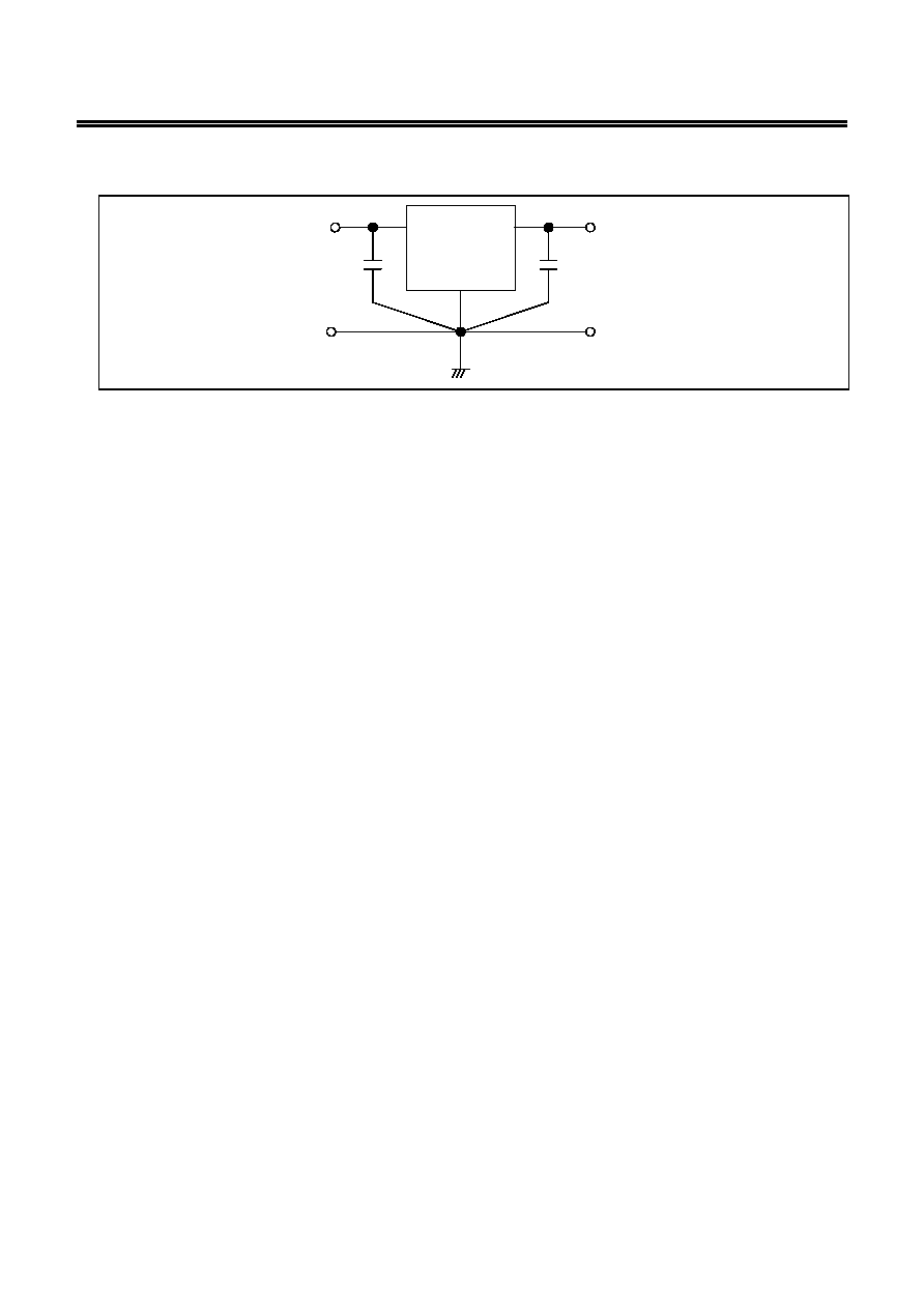
Standard Circuit
VSS
VOUT
VIN
C
IN
*1
C
L
*2
INPUT
OUTPUT
GND
Single GND
*1. C
IN
is a capacitor used to stabilize input.
*2. In addition to a tantalum capacitor, a ceramic capacitor of 0.47
µF or more can be used in C
L
.
Figure 11
Caution The above connection diagram and constant will not guarantees successful operation.
Perform through evaluation using the actual application to set the constant.
Technical Terms
1. Low dropout voltage regulator
The low dropout voltage regulator is a voltage regulator featuring a low dropout voltage characteristic due
to its internal low ON-resistance characteristic transistors.
2. Low ESR
ESR is the abbreviation for Equivalent Series Resistance. The low ESR output capacitor (C
L
) can be
used in the S-814 Series.
3. Output voltage (V
OUT
)
The accuracy of the output voltage is ensured at
±2.0 % under the specified conditions
*1
of input voltage,
output current, and temperature, which differ depending upon the product items.
*1. The condition differs depending upon each product.
Caution If you change the above conditions, the output voltage value may vary out of the
accuracy range of the output voltage. Refer to the " Electrical Characteristics" and
" Characteristics" for details.
4. Line regulation 1 (
V
OUT1
) and Line regulation 2 (
V
OUT2
)
Indicate the input voltage dependencies of output voltage. That is, the values show how much the output
voltage changes due to a change in the input voltage with the output current remained unchanged.
5. Load regulation (
V
OUT3
)
Indicates the output current dependencies of output voltage. That is, the values show how much the
output voltage changes due to a change in the output current with the input voltage remained unchanged.
LOW DROPOUT CMOS VOLTAGE REGULATOR
Rev.1.5
_00
S-814 Series
12
Seiko Instruments Inc.
6. Dropout voltage (V
drop
)
Indicates a difference between input voltage (V
IN1
) and output voltage when output voltage falls by 98 %
of V
OUT(E)
by gradually decreasing the input voltage.
V
drop
=V
IN1
-(V
OUT(E)
◊0.98)
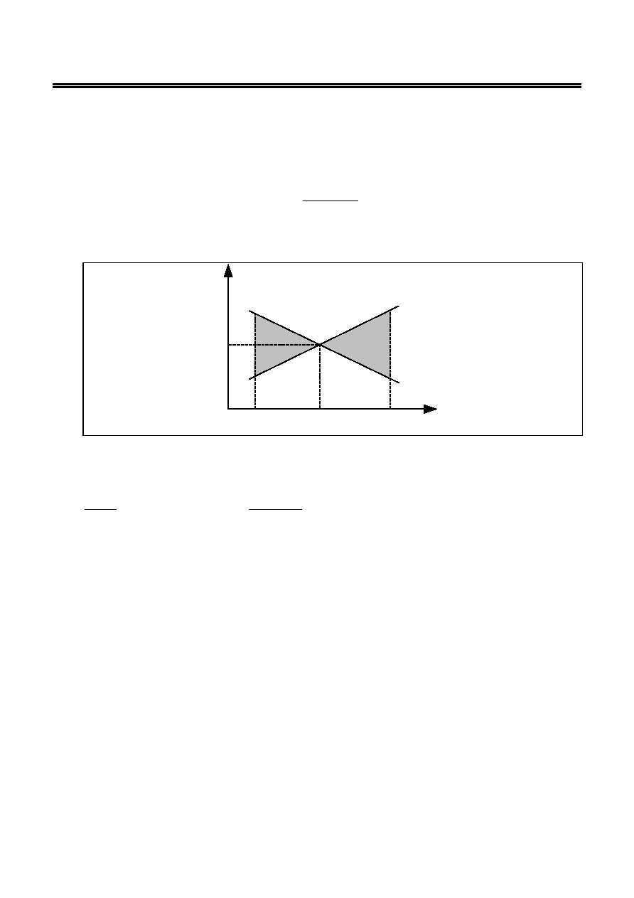
7. Temperature coefficient of output voltage
∑
∑
∑
∑
OUT
OUT
V
Ta
V
The shadowed area in Figure 12 is the range where V
OUT
varies in the operating temperature range when
the temperature coefficient of the output voltage is
±100 ppm/∞C.
-40 25
+0.28 mV/∞C
V
OUT
[V]
V
OUT(E)
*1
85
Ta [
∞C]
-0.28mV/∞C
*1. The mesurement value of output voltage at 25
∞C.
Figure 12 Typical example of the S-814A28A
A change in temperatures of output voltage [mV/∞C] is calculated using the following equation.
[
]
[ ]
[
]
1000
C
/
ppm
V
Ta
V
V
V
C
/
mV
Ta
V
OUT
OUT
)
S
(
OUT
OUT
˜
∞
∑
◊
=
∞
3
*
2
*
*1
*1. The change in temperature of the dropout voltage
*2. Specified output voltage
*3. Output voltage temperature coefficient
Rev.1.5
_00
LOW DROPOUT CMOS VOLTAGE REGULATOR
S-814 Series
Seiko Instruments Inc.
13
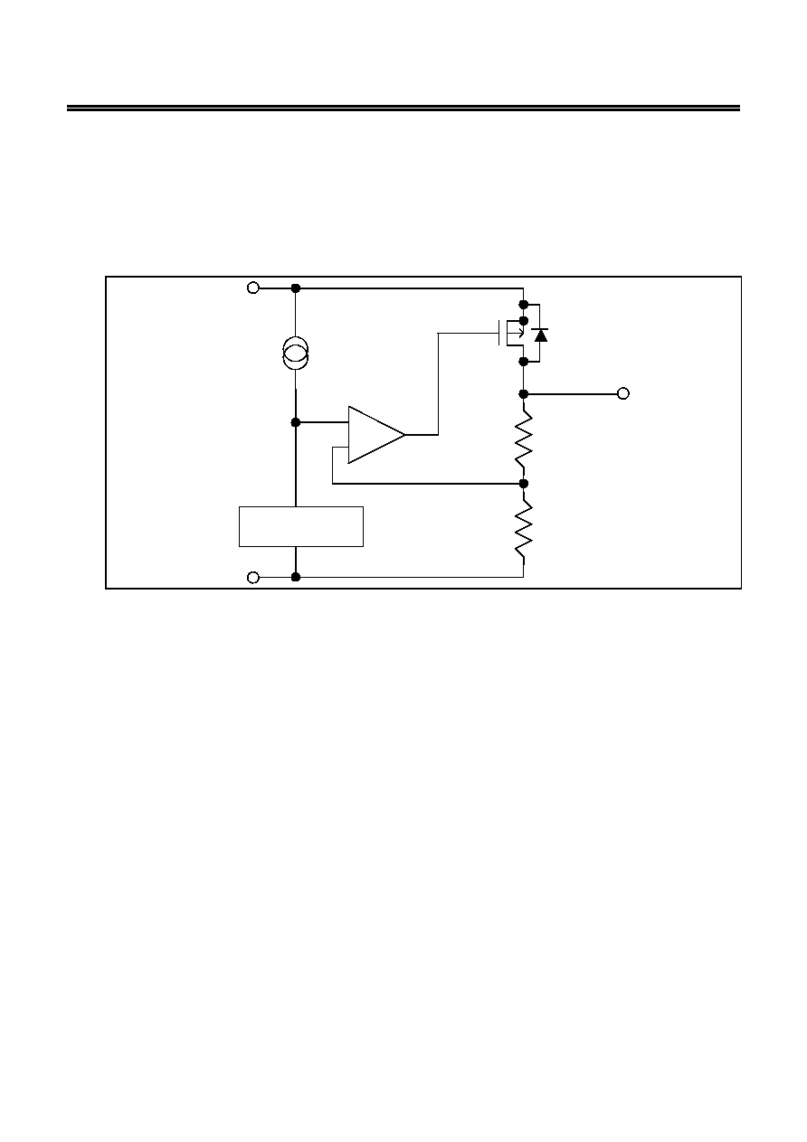
Operation
1. Basic operation
Figure 13 shows the block diagram of the S-814 Series.
The error amplifier compares a reference voltage V
ref
with part of the output voltage divided by the
feedback resistors R
s
and R
f
. It supplies the output transistor with the gate voltage, necessary to ensure
certain output voltage free of any fluctuations of input voltage and temperature.
VOUT
*1
VSS
VIN
Rs
R
f
Error amplifier
Current source
V
ref
-
+
Reference voltage
circuit
*1. Parasitic diode
Figure 13
2. Output transistor
The S-814 Series uses a low on-resistance Pch MOS FET as the output transistor.
Be sure that V
OUT
does not exceed V
IN
+0.3 V to prevent the voltage regulator from being broken due to
inverse current flowing from VOUT pin through a parasitic diode to VIN pin.

LOW DROPOUT CMOS VOLTAGE REGULATOR
Rev.1.5
_00
S-814 Series
14
Seiko Instruments Inc.
3. ON/OFF pin (Shutdown pin)
*1
This pin starts and stops the regulator.
When the shutdown pin is switched to the shutdown level, the operation of all internal circuits stops, the
built-in Pch MOSFET output transistor between VIN pin and VOUT pin is shutdown, allowing current
consumption to be drastically reduced. The VOUT pin enters the Vss level due to internally divided
resistance of several M
between VOUT pin and VSS pin.
Furthermore, the structure of the ON/OFF pin is as shown in Figure 14. Since the ON/OFF pin is neither
pulled down nor pulled up internally, do not use it in the floating state. In addition, please note that current
consumption increases if a voltage of 0.3 V to V
IN
-0.3 V is applied to the shutdown pin. When the
ON/OFF pin is not used, connect it to the VIN pin in case of the product type is `"A" and to the VSS pin in
case of "B".
V
IN
ON/OFF
V
SS
Figure 14
Table 8
Product type
ON/OFF pin
Internal circuit
VOUT pin voltage Current consumption
A
"H": Power on
Operating
Set value
I
SS1
A
"L": Shutdown
Stop
V
SS
level
I
SS2
B
"H": Shutdown
Stop
V
SS
level
I
SS2
B
"L": Power on
Operating
Set value
I
SS1
*1. ON/OFF pin (Shutdown pin) is not in S-814AxxAUA Series.
4. Short-circuit protection circuit
The S-814 Series incorporates a short-circuit protection circuit to protect the output transistor against
short-circuiting between VOUT pin and VSS pin.
The short-circuit protection circuit controls output current as shown in "1. Output voltage vs. Output
current (When load current increases)" curve in " Characteristics", and prevents output current of
approx. 70 mA or more from flowing even if VOUT pin and VSS pin are shorted. However, the short-
circuit protection circuit does not protect thermal shutdown. Be sure that input voltage and load current do
not exceed the specified power dissipation level.
When output current is large and a difference between input and output voltages is large even if not
shorted, the short-circuit protection circuit may start functioning and the output current may be controlled
to the specified amperage. For details, refer to "3. Maximum output current vs. Input voltage" curve in
" Characteristics".

Rev.1.5
_00
LOW DROPOUT CMOS VOLTAGE REGULATOR
S-814 Series
Seiko Instruments Inc.
15
Selection of Output Capacitor (C
L
)
Mount an output capacitor between VOUT pin and VSS pin for phase compensation. The S-814 Series
enables customers to use a ceramic capacitor as well as a tantalum or an aluminum electrolytic capacitor.
∑ A ceramic capacitor or an OS capacitor:
Use a capacitor of 0.47
µF or more.
∑ A tantalum or an aluminum electrolytic capacitor:
Use a capacitor of 0.47
µF or more and ESR of 10 or less.
Pay special attention not to cause an oscillation due to an increase in ESR at low temperatures, when
you use the aluminum electrolytic capacitor. Evaluate the capacitor taking into consideration its
performance including temperature characteristics.
Overshoot and undershoot characteristics differ depending upon the type of the output capacitor you
select. Refer to "C
L
dependencies of overshoot" and "C
L
dependencies of undershoot" in
" Transient Response Characteristics".
Precautions
∑ Wiring patterns for VIN pin, VOUT pin and GND pin should be designed so that the impedance is low.
When mounting an output capacitor, the distance from the capacitor to the VOUT pin and the VSS pin
should be as short as possible.
∑ Note that output voltage may increase when a series regulator is used at low load current. (Less than
10
µA)
∑ Generally, a series regulator may cause oscillation, depending on the selection of external parts. The
following conditions are recommended for this IC. However, be sure to perform sufficient evaluation under
the actual usage conditions to select the series regulator.
Output capacitor (C
L
):
0.47
µF or more
Equivalent Series Resistance (ESR): 10
or less
Input series resistance (R
IN
):
10
or less
∑ The voltage regulator may oscillate when the impedance of the power supply is high and the input
capacitor is small or an input capacitor is not connected.
∑ The application conditions for input voltage and load current do not exceed the power dissipation level of
the package.
∑ In determining the output current, attention should be paid to the output current value specified and
footnote *5 in Table 6 and Table 7 in the " Electrical Characteristics".
∑ Do not apply an electrostatic discharge to this IC that exceeds the performance ratings of the built-in
electrostatic protection circuit.
∑ SII claims no responsibility for any and all disputes arising out of or in connection with any infringement by
products including this IC of patents owned by a third party.
LOW DROPOUT CMOS VOLTAGE REGULATOR
Rev.1.5
_00
S-814 Series
16
Seiko Instruments Inc.
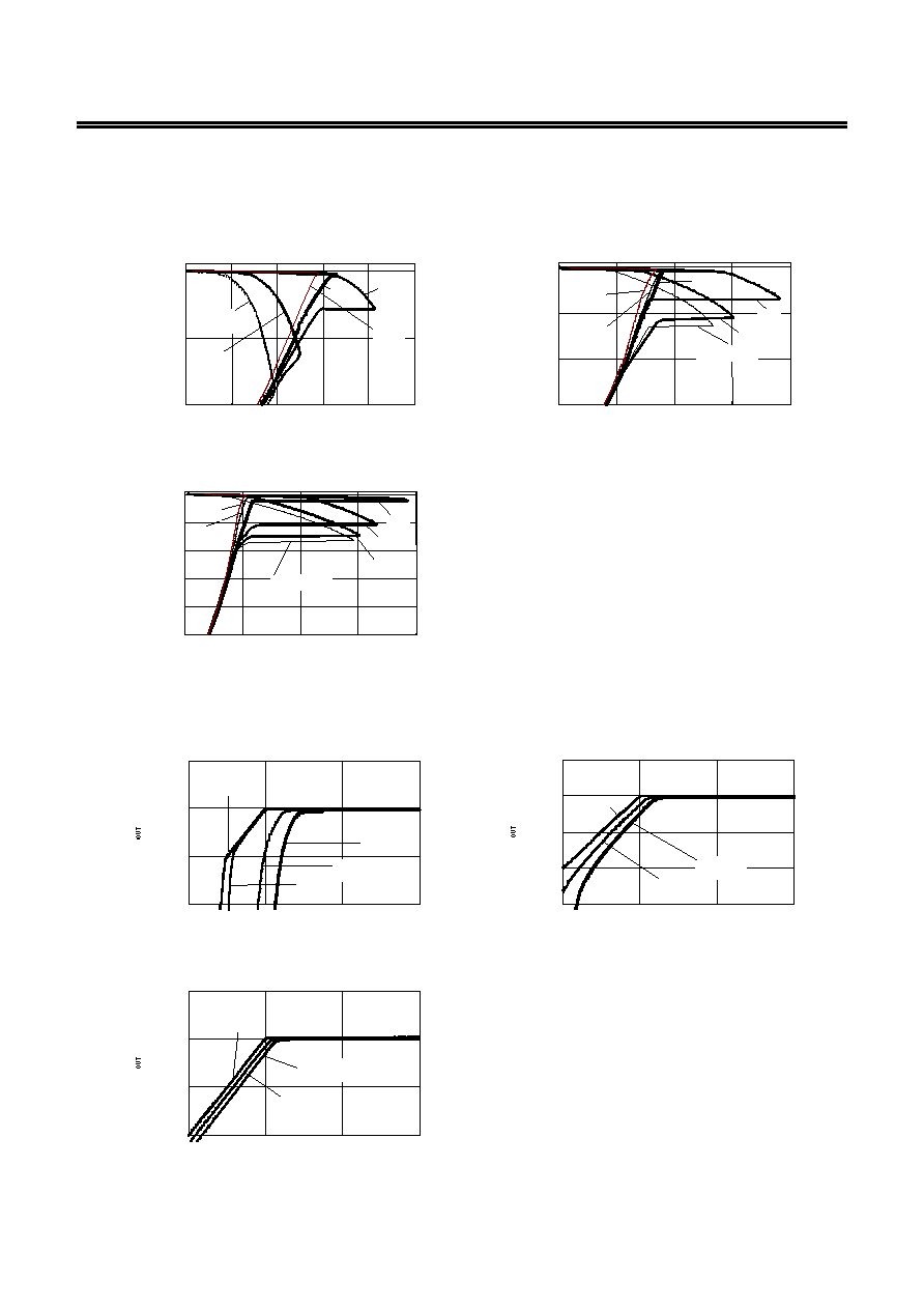
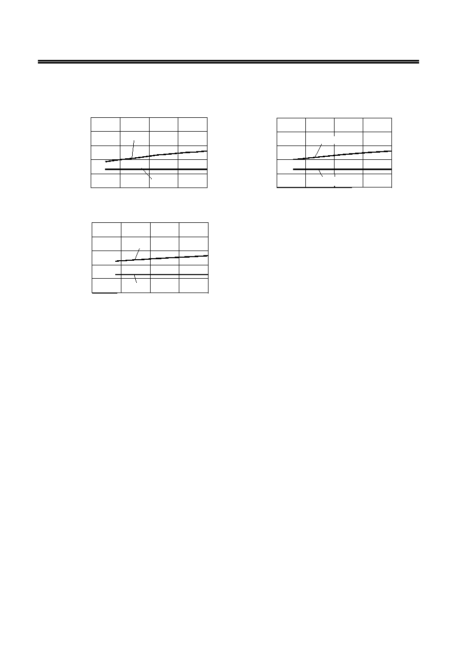
Characteristics (Typical data)
1. Output voltage (V
OUT
) vs. Output current (I
OUT
) (When load current increases)
S-814A20A S-814A30A
(Ta
=25∞C)
0
1.0
2.0
0 50 100 150 200 250
I
OUT
[mA]
V
OU
T
[V
]
3 V
V
IN
=2.3 V
2.5
V
10 V
4 V
(Ta=25∞C)
0
1.0
2.0
3.0
0 100 200 300 400
I
OUT
[mA]
V
OU
T
[
V
]
V
IN
=3.3 V
4 V
5 V
3.5 V
6 V
10 V
S-814A50A
(Ta=25∞C)
0
1.0
2.0
3.0
4.0
5.0
0 200 400 600 800
I
OUT
[mA]
V
OU
T
[
V
]
V
IN
=5.3 V
6 V
7 V
5.5 V
10 V
8 V
Remark In determining the output current, attention
should be paid to the following.
1. The minimum output current value and
footnote *5 in the " Electrical
characteristics".
2. The package power dissipation.
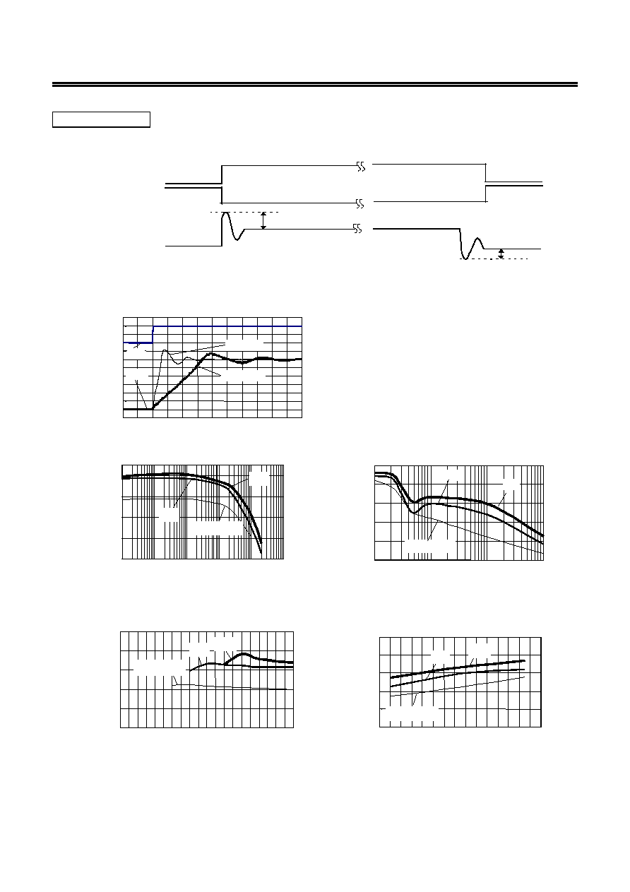
2. Output voltage (V
OUT
) vs. Input voltage (V
IN
)
S-814A20A (Ta=25∞C)
1.0
1.5
2.0
2.5
1
2
3
4
V
IN
(V)
V
(V)
60mA
Iout=10uA
1mA
30mA
100uA
S-814A30A (Ta=25∞C)
1.5
2.0
2.5
3.0
3.5
2
3
4
5
V
IN
(V)
V
(V)
30mA
60mA
Iout=10uA
1mA
100uA
S-814A50A (Ta=25∞C)
4.0
4.5
5.0
5.5
4
5
6
7
V
IN
(V)
V
(V)
30mA
60mA
1mA
Iout=10uA
100uA
Rev.1.5
_00
LOW DROPOUT CMOS VOLTAGE REGULATOR
S-814 Series
Seiko Instruments Inc.
17
3. Maximum output current (I
OUTmax
) vs. Input voltage (V
IN
)
S-814A20A S-814A30A
0
100
200
300
1 2 3 4 5 6 7 8 9 10
V
IN
[V]
I
OU
T
m
a
x
[m
A]
Ta
=-40∞C
25∞C
85∞C
0
200
400
600
2 3 4 5 6 7 8 9 10
V
IN
[V]
I
OU
Tm
a
x
[m
A
]
Ta
=-40∞C
25∞C
85∞C
S-814A50A
0
200
400
600
800
4 5 6 7 8 9 10
V
IN
[V]
I
OU
Tm
a
x
[m
A]
Ta
=-40∞C
25∞C
85∞C
Remark In determining the output current, attention
should be paid to the following.
1. The minimum output current value and
footnote *5 in the " Electrical
characteristics".
2. The package power dissipation.
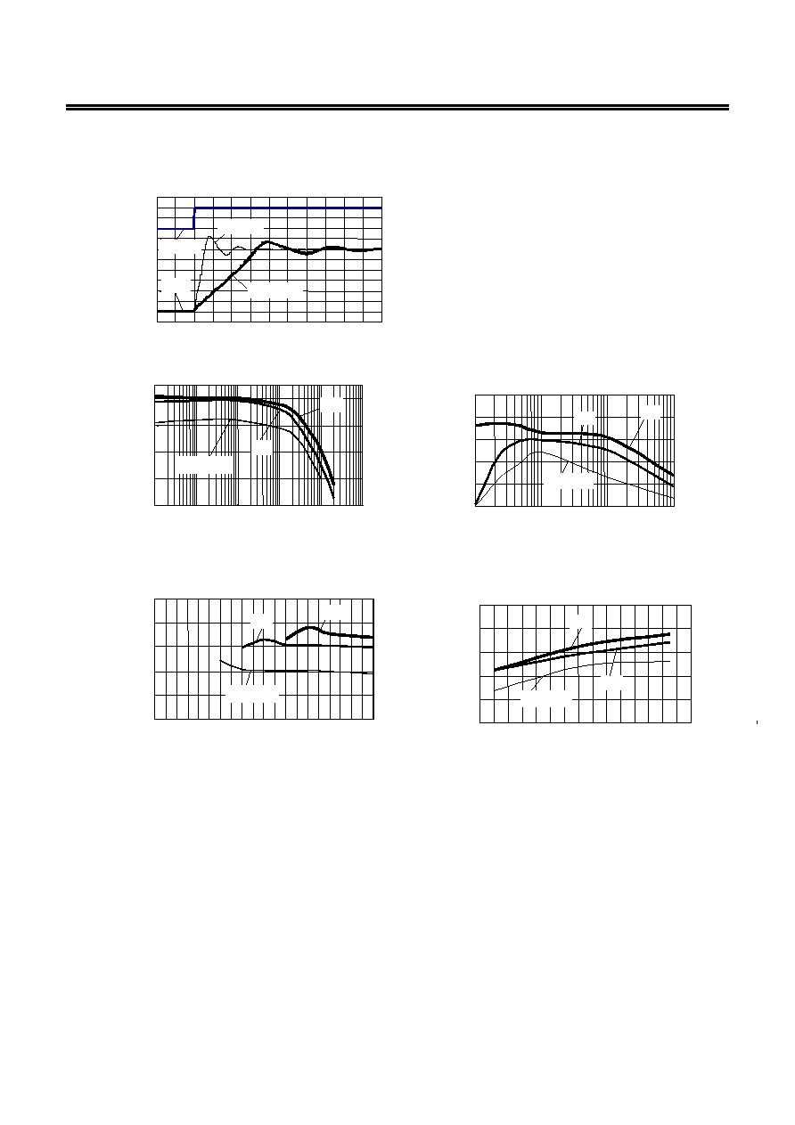
4. Dropout voltage (V
drop
) vs. Output current (I
OUT
)
S-814A20A S-814A30A
0
50
100
150
200
250
300
0 5 10 15 20 25 30
I
OUT
[mA]
V
drop
[m
V]
Ta
=-40∞C
25∞C
85∞C
0
30
60
90
120
0 5 10 15 20 25 30
I
OUT
[mA]
V
drop
[m
V]
25∞C
Ta
=-40∞C
85∞C
S-814A50A
0
40
80
120
160
0 10 20 30 40 50 60
I
OUT
[mA]
V
drop
[m
V]
Ta
=-40∞C
25∞C
85∞C
LOW DROPOUT CMOS VOLTAGE REGULATOR
Rev.1.5
_00
S-814 Series
18
Seiko Instruments Inc.
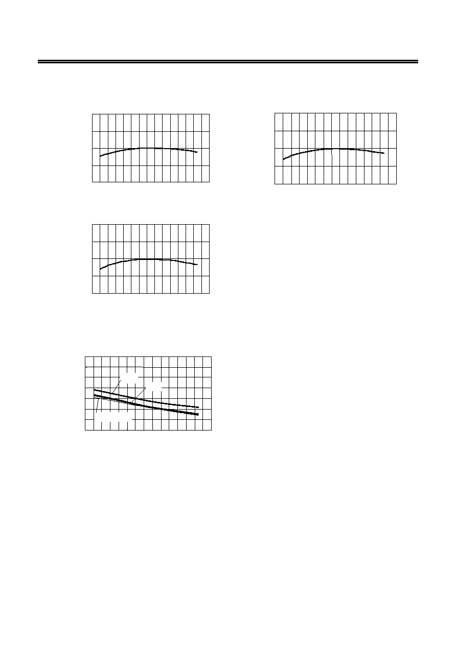
5. Output voltage (V
OUT
) vs. Ambient temperature (Ta)
S-814A20A S-814A30A
1.96
1.98
2.00
2.02
2.04
-50
0 50 100
Ta [∞C]
V
OU
T
[
V
]
V
IN
=3V, I
OUT
=30mA
2.94
2.97
3.00
3.03
3.06
-50
0 50 100
Ta [∞C]
V
OUT
[
V
]
V
IN
=4V, I
OUT
=30mA
S-814A50A
4.90
4.95
5.00
5.05
5.10
-50
0 50 100
Ta [∞C]
V
OU
T
[V
]
V
IN
=6V, I
OUT
=30mA
6. Line regulation (
V
OUT1
) vs. Ambient temperature (Ta)
S-814A20A/S-814A30A/S-814A50A
0
5
10
15
20
25
30
35
-50
0 50 100
Ta [∞C]
3 V
V
OUT
=2 V
5 V
V
IN
=V
OUT(S)
+0.510 V, I
OUT
=30 mA
V
OUT1
[m
V]
Rev.1.5
_00
LOW DROPOUT CMOS VOLTAGE REGULATOR
S-814 Series
Seiko Instruments Inc.
19
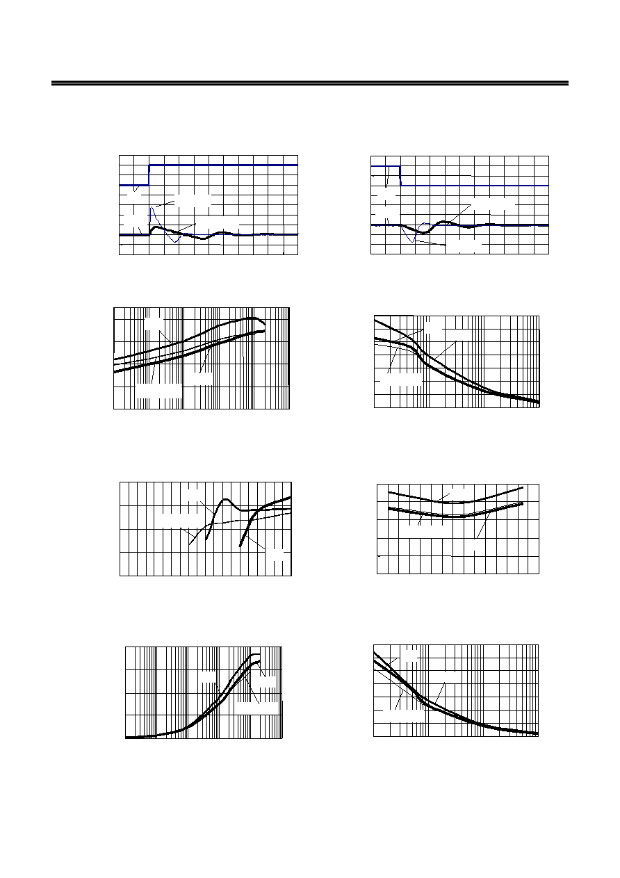
7. Load regulation (
V
OUT3
) vs. Ambient temperature (Ta)
S-814A20A/S-814A30A/S-814A50A
0
10
20
30
40
50
-50
0 50 100
Ta [∞C]
3 V
5 V
V
OUT
=2 V
V
IN
=V
OUT(S)
+1 V, I
OUT
=10 µA80 mA
V
OUT3
[m
V]
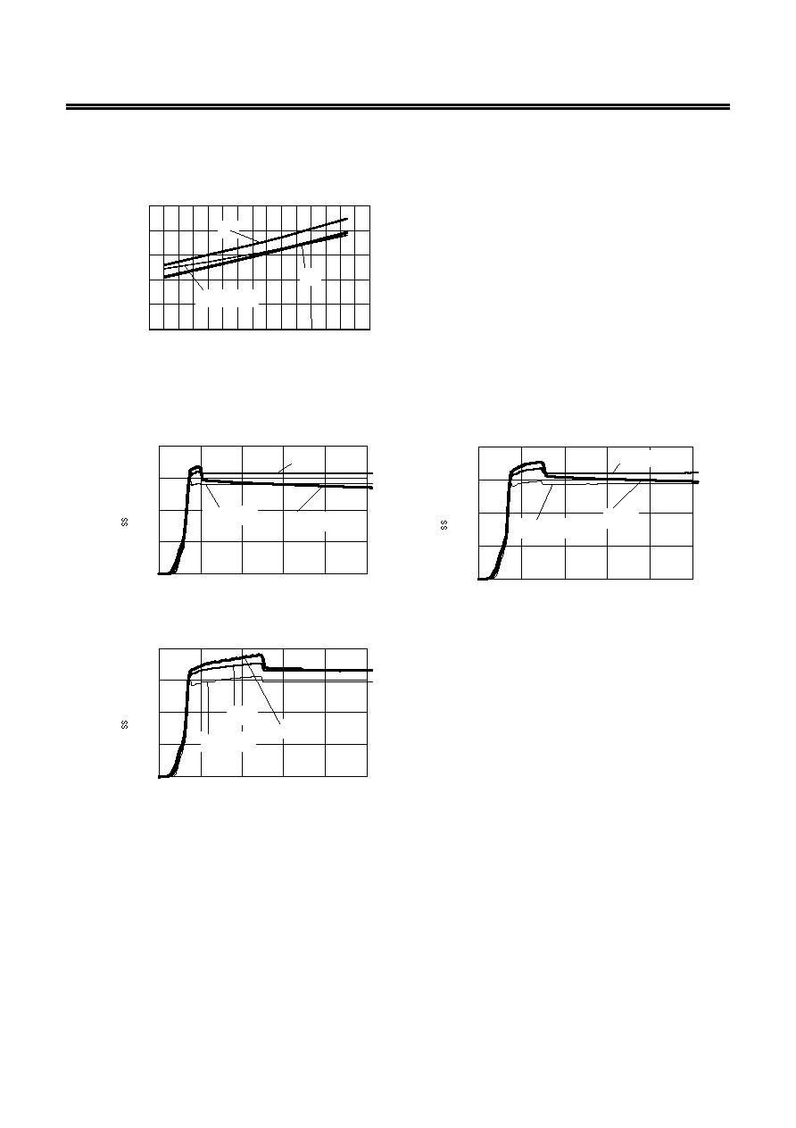
8. Current consumption (I
SS1
) vs. Input voltage (V
IN
)
S-814A20A
0
10
20
30
40
0
2
4
6
8
10
V
IN
(V)
I
1(uA)
Ta=-40∞C
85∞C
25∞C
S-814A30A
0
10
20
30
40
0
2
4
6
8
10
V
IN
(V)
I
1(uA)
Ta=-40∞C
85∞C
25∞C
S-814A50A
0
10
20
30
40
0
2
4
6
8
10
V
IN
(V)
I
1(uA)
Ta=-40∞C
85∞C
25∞C
LOW DROPOUT CMOS VOLTAGE REGULATOR
Rev.1.5
_00
S-814 Series
20
Seiko Instruments Inc.
9. Threshold voltage of shutdown pin (V
SH
/V
SL
) vs. Input voltage (V
IN
) (With shutdown function
product)
S-814A20A S-814A30A
0
0.5
1.0
1.5
2.0
2.5
2 4 6 8 10
V
IN
[V]
V
SH
/V
SL
[
V
]
V
SH
V
SL
0
0.5
1.0
1.5
2.0
2.5
3 5 7 8 10
V
IN
[V]
V
SH
/V
SL
[
V
]
V
SH
V
SL
S-814A50A
0
0.5
1.0
1.5
2.0
2.5
5 6 8 9 10
V
IN
[V]
V
SH
/V
SL
[
V
]
V
SL
V
SH
Rev.1.5
_00
LOW DROPOUT CMOS VOLTAGE REGULATOR
S-814 Series
Seiko Instruments Inc.
21
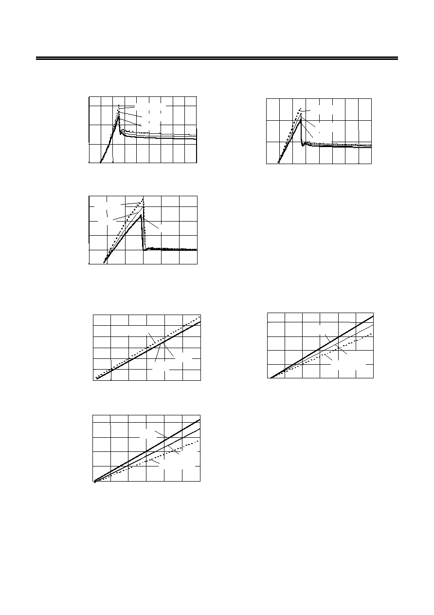
Reference data
Transient Response Characteristics (S-814A30A, Typical data, Ta
=
=
=
=25∞∞∞∞C)
Overshoot
Input voltage
or
Load current
Output volatage
Undershoot
1. At power on
Output voltage (V
OUT
) ≠ Time (t)
V
IN
=010 V, I
OUT
=30 mA
t [50
µs/div]
V
OU
T
[
0
.5
V/d
i
v
]
0 V
0 V
10 V
C
L
=4.7 µF
C
L
=
=1 µF
V
OUT
V
IN
Load dependencies of overshoot
C
L
dependencies of overshoot
0
0.2
0.4
0.6
0.8
1.E
-05
1.E
-04
1.E
-03
1.E
-02
1.E
-01
1.E
+00
I
OUT
[A]
O
v
e
r
s
hoot
[
V
]
5 V
V
IN
=0V
OUT(S)
+1 V, C
L
=1 µF
3 V
V
OUT
=2 V
0
0.2
0.4
0.6
0.8
1.0
0.1 1 10 100
C
L
[uF]
Overs
hoot
[
V
]
V
OUT
=2 V
5 V
3 V
V
IN
=0V
OUT(S)
+1 V, I
OUT
=30 mA
V
DD
dependencies of overshoot
Temperature dependencies of overshoot
0
0.2
0.4
0.6
0.8
1.0
0 2 4 6 8
10
V
DD
[V]
O
v
ers
h
oot
[V
]
V
IN
=0V
DD
, I
OUT
=30 mA, C
L
=1 µF
V
OUT
=2 V
3 V 5 V
0
0.2
0.4
0.6
0.8
1.0
-50
0 50
100
Ta [∞C]
O
ver
s
h
o
o
t
[
V
]
V
IN
=0V
OUT(S)
+1 V, I
OUT
=30 mA, C
L
=1 µF
V
OUT
=2 V
3 V
5 V
LOW DROPOUT CMOS VOLTAGE REGULATOR
Rev.1.5
_00
S-814 Series
22
Seiko Instruments Inc.
2. At power on/off control (With shutdown function product)
Output voltage (V
OUT
) ≠ Time (t)
V
IN
=10 V, ON/OFF=010 V, I
OUT
=30 mA
t [50
µs/div]
V
OU
T
[
0
.5
V/
d
i
v
]
10 V
0 V
0 V
C
L
=4.7 µF
C
L
=1 µF
V
OUT
ON/OFF
Load dependencies of overshoot
C
L
dependencies of overshoot
0
0.2
0.4
0.6
0.8
1.E
-05
1.E
-04
1.E
-03
1.E
-02
1.E
-01
1.E
+00
I
OUT
[A]
O
v
e
r
sh
o
o
t [
V
]
5 V
V
OUT
=2 V
3 V
V
IN
=V
OUT(S)
+1 V
, C
L
=1 µF, ON/OFF=0V
OUT(S)
+1 V
0
0.2
0.4
0.6
0.8
1.0
0.1 1 10 100
C
L
[
µF]
O
v
er
shoot
[
V
]
V
IN
=V
OUT(S)
+1 V, I
OUT
=30 mA, ON/OFF=0V
OUT(S)
+1V
V
OUT
=2 V
3 V
5 V
V
DD
dependencies of overshoot
Temperature dependencies of overshoot
0
0.2
0.4
0.6
0.8
1.0
0 2 4 6 8 10
V
DD
[V]
O
v
e
r
sh
o
o
t [V
]
V
IN
=V
DD
, I
OUT
=30 mA, C
L
=1 µF, ON/OFF=0V
DD
V
OUT
=2 V
5 V
3 V
0
0.2
0.4
0.6
0.8
1.0
-50
0 50 100
Ta [
∞C]
Ov
ersh
oo
t
[V
]
5 V
3 V
V
IN
=V
OUT(S)
+1 V, I
OUT
=30 mA, C
L
=1 µF,
ON/OFF
=0V
OUT(S)
+1V
V
OUT
=2 V
Rev.1.5
_00
LOW DROPOUT CMOS VOLTAGE REGULATOR
S-814 Series
Seiko Instruments Inc.
23
3. At power fluctuation
Output voltage (V
OUT
) ≠ Time (t)
V
IN
=4.010 V, I
OUT
=30 mA
t [50
µs/div]
V
OU
T
[0.
5
V
/
di
v
]
3 V
C
L
=4.7 µF
C
L
=1 µF
V
IN
4 V
10 V
V
OUT
V
IN
=104.0 V, I
OUT
=30 mA
t [50
µs/div]
V
OU
T
[0
.5
V
/
div
]
3 V
4 V
10 V
V
IN
C
L
=4.7 µF
C
L
=1 µF
V
OUT
Load dependencies of overshoot
C
L
dependencies of overshoot
0
0.2
0.4
0.6
0.8
1.E
-05
1.E
-04
1.E
-03
1.E
-02
1.E
-01
1.E
+00
I
OUT
[A]
O
v
er
s
hoot
[V
]
5 V
V
IN
=V
OUT(S)
+1 VV
OUT(S)
+2 V, C
L
=1 µF
V
OUT
=2 V
3 V
0
0.2
0.4
0.6
0.8
1.0
1.2
1.4
0.1 1 10 100
C
L
[
µF]
O
v
ersho
o
t
[V]
5 V
3 V
V
OUT
=2 V
V
IN
=V
OUT(S)
+1 VV
OUT(S)
+2 V, I
OUT
=30 mA
V
DD
dependencies of overshoot
Temperature dependencies of overshoot
0
0.5
1.0
1.5
2.0
0 2 4 6 8 10
V
DD
[V]
O
v
e
r
sh
o
o
t [V
]
V
IN
=V
OUT(S)
+1 VV
DD
, I
OUT
=30 mA, C
L
=1 µF
V
OUT
=2 V
3 V
5 V
0
0.2
0.4
0.6
0.8
1.0
-50
0 50 100
Ta [
∞C]
O
v
er
shoot
[
V
]
5 V
3 V
V
OUT
=2 V
V
IN
=V
OUT(S)
+1 VV
OUT(S)
+2 V, I
OUT
=30 mA, C
L
=1 µF
Load dependencies of undershoot
C
L
dependencies of undershoot
0
0.2
0.4
0.6
0.8
1.E
-05
1.E
-04
1.E
-03
1.E
-02
1.E
-01
1.E
+00
I
OUT
[A]
U
n
de
rsh
oot
[V]
5 V
V
OUT
=2 V
V
IN
=V
OUT(S)
+2 VV
OUT(S)
+1 V, C
L
=1 µF
3 V
0
0.2
0.4
0.6
0.8
1.0
1.2
1.4
0.1 1 10 100
C
L
[
µF]
Undersh
oo
t [V
]
5 V
3 V
V
OUT
=2 V
V
IN
=V
OUT(S)
+2 VV
OUT(S)
+1 V, I
OUT
=30 mA
LOW DROPOUT CMOS VOLTAGE REGULATOR
Rev.1.5
_00
S-814 Series
24
Seiko Instruments Inc.
V
DD
dependencies of undershoot
Temperature dependencies of undershoot
0
0.2
0.4
0.6
0.8
1.0
0 2 4 6 8 10
V
DD
[V]
U
n
d
e
r
s
h
o
o
t [V
]
5 V
3 V
V
IN
=V
DD
V
OUT(S)
+1 V, I
OUT
=30 mA, C
L
=1 µF
V
OUT
=2 V
0
0.2
0.4
0.6
0.8
1.0
-50
0 50 100
Ta [
∞C]
Unde
rsho
o
t
[V]
5 V
3 V
V
OUT
=2 V
V
IN
=V
OUT(S)
+2 VV
OUT(S)
+1 V, I
OUT
=30 mA, C
L
=1 µF
Rev.1.5
_00
LOW DROPOUT CMOS VOLTAGE REGULATOR
S-814 Series
Seiko Instruments Inc.
25
4. At load fluctuation
Output voltage (V
OUT
) ≠ Time (t)
I
OUT
=10 µA30 mA, V
IN
=4 V
t [20
µs/div]
V
OU
T
[0.
2
V
/
div]
30 mA
V
OUT
I
OUT
3 V
10
µA
C
L
=4.7 µF
C
L
=1 µF
I
OUT
=30 mA10 µA, V
IN
=4 V
t [20 ms/div]
V
OU
T
[0.1 V
/
di
v]
30 mA
V
OUT
I
OUT
3 V
10
µA
C
L
=1 µF
C
L
=4.7 µF
Load current dependencies of overshoot
C
L
dependencies of overshoot
0
0.2
0.4
0.6
0.8
1
1.E
-03
1.E
-02
1.E
-01
1.E
+00
I
OUT
[A]
O
v
er
shoot
[
V
]
5 V
V
OUT
=2 V
V
IN
=V
OUT(S)
+1 V, C
L
=1 µF
3 V
Remark
I
OUT
shows larger load current at load
current fluctuation. Smaller current at load
current fluctuation is fixed to 10 µA.
i.e.
I
OUT
=1.E-02 [A] means load current
fluctuation from 10 mA to 10 µA.
0
0.2
0.4
0.6
0.8
1.0
0.1 1 10 100
C
L
[
µF]
Ov
ersh
oo
t
[
V
]
5 V
3 V
V
IN
=V
OUT(s)
+1 V, I
OUT
=30 mA10 µA
V
OUT
=2 V
V
DD
dependencies of overshoot
Temperature dependencies of overshoot
0
0.2
0.4
0.6
0.8
1.0
0 2 4 6 8 10
V
DD
[V]
O
v
e
r
sh
o
o
t [V
]
5 V
3 V
V
OUT
=2 V
V
IN
=V
DD
, I
OUT
=30 mA10 µA, C
L
=1 µF
0
0.2
0.4
0.6
0.8
1.0
-50
0 50 100
Ta [∞C]
Ov
ersho
o
t
[
V
]
3 V
V
IN
=V
OUT(S)
+1 V, I
OUT
=30 mA10 µA, C
L
=1 µF
V
OUT
=2 V
5 V

LOW DROPOUT CMOS VOLTAGE REGULATOR
Rev.1.5
_00
S-814 Series
26
Seiko Instruments Inc.
Load current dependencies of undershoot
C
L
dependence of undershoot
0
0.2
0.4
0.6
0.8
1
1.2
1.4
1.E
-03
1.E
-02
1.E
-01
1.E
+00
I
OUT
[A]
Unders
h
o
o
t
[
V
]
V
IN
=V
OUT(S)
+1 V, C
L
=1 µF
3 V
5 V
V
OUT
=2 V
Remark
I
OUT
shows larger load current at load
current fluctuation. Lower current at load
current fluctuation is fixed to 10 µA.
i.e.
I
OUT
=1.E-02 [A] means load current
fluctuation from 10 µA to 10 mA.
0
0.2
0.4
0.6
0.8
1.0
1.2
0.1 1 10 100
C
L
[
µF]
Under
sho
o
t
[
V
]
5 V
V
IN
=V
OUT(S)
+1 V, I
OUT
=10 µA30 mA
3 V
V
OUT
=2 V
V
DD
dependencies of undershoot
Temperature dependencies of undershoot
0
0.2
0.4
0.6
0.8
1.0
0 2 4 6 8 10
V
DD
[V]
U
ndershoot [
V
]
5 V
3 V
V
IN
=V
DD
, I
OUT
=10 µA30 mA, C
L
=1 µF
V
OUT
=2 V
0
0.2
0.4
0.6
0.8
1.0
-50
0 50 100
Ta [
∞C]
U
n
de
r
s
ho
ot
[
V
]
V
IN
=V
OUT(S)
+1 V, I
OUT
=10 µA30 mA, C
L
=1 µF
V
OUT
=2 V
3 V
5 V
No.
TITLE
SCALE
UNIT
mm
Seiko Instruments Inc.
2.9±0.2
1.9±0.2
0.95±0.1
0.4±0.1
0.16
+0.1
-0.06
1
2
3
4
5
No. MP005-A-P-SD-1.2
MP005-A-P-SD-1.2
SOT235-A-PKG Dimensions
No.
TITLE
SCALE
UNIT
mm
Seiko Instruments Inc.
¯1.5
+0.1
-0
2.0±0.05
¯1.0
+0.2
-0
4.0±0.1
1.4±0.2
0.25±0.1
3.2±0.2
1
2
3
4
5
No. MP005-A-C-SD-2.1
MP005-A-C-SD-2.1
SOT235-A-Carrier Tape
Feed direction
4.0±0.1(10 pitches:40.0±0.2)

No.
TITLE
SCALE
UNIT
mm
Seiko Instruments Inc.
12.5max.
9.0±0.3
¯13±0.2
(60∞)
(60∞)
QTY.
3,000
No. MP005-A-R-SD-1.1
MP005-A-R-SD-1.1
SOT235-A-Reel
Enlarged drawing in the central part
No.
TITLE
SCALE
UNIT
mm
Seiko Instruments Inc.
0.4±0.05
1.5±0.1
4.5±0.1
1.6±0.2
1.5±0.1 1.5±0.1
0.45±0.1
0.4±0.1
0.4±0.1
45∞
3
1
2
No. UP003-A-P-SD-1.1
UP003-A-P-SD-1.1
SOT893-A-PKG Dimensions
No.
TITLE
SCALE
UNIT
mm
Seiko Instruments Inc.
2.0±0.1
0.3±0.05
8.0±0.1
¯1.5
+0.1
-0
2.0±0.05
¯1.5
+0.1
-0
4.75±0.1
5∞ max.
No. UP003-A-C-SD-1.1
UP003-A-C-SD-1.1
SOT893-A-Carrier Tape
Feed direction
4.0±0.1(10 pitches : 40.0±0.2)

No.
TITLE
SCALE
UNIT
mm
Seiko Instruments Inc.
13.0±0.3
16.5max.
(60∞)
(60∞)
QTY.
1,000
No. UP003-A-R-SD-1.1
UP003-A-R-SD-1.1
SOT893-A-Reel
Enlarged drawing in the central part
No.
TITLE
SCALE
UNIT
mm
Seiko Instruments Inc.
1.5±0.1 1.5±0.1
1.6±0.2
4.5±0.1
1
3
2
1.5±0.1
0.4±0.05
0.4±0.1
0.45±0.1
0.4±0.1
45∞
0.3
5
4
No. UP005-A-P-SD-1.1
UP005-A-P-SD-1.1
SOT895-A-PKG Dimensions

No.
TITLE
SCALE
UNIT
mm
Seiko Instruments Inc.
2.0±0.1
0.3±0.05
8.0±0.1
¯1.5
+0.1
-0
2.0±0.05
¯1.5
+0.1
-0
4.75±0.1
5∞ max.
1
3 2
5
4
No. UP005-A-C-SD-1.1
UP005-A-C-SD-1.1
SOT895-A-Carrier Tape
Feed direction
4.0±0.1(10 pitches : 40.0±0.2)
No.
TITLE
SCALE
UNIT
mm
Seiko Instruments Inc.
16.5max.
13.0±0.3
QTY.
1,000
(60∞)
(60∞)
No. UP005-A-R-SD-1.1
UP005-A-R-SD-1.1
SOT895-A-Reel
Enlarged drawing in the central part

∑
The information described herein is subject to change without notice.
∑
Seiko Instruments Inc. is not responsible for any problems caused by circuits or diagrams described herein
whose related industrial properties, patents, or other rights belong to third parties. The application circuit
examples explain typical applications of the products, and do not guarantee the success of any specific
mass-production design.
∑
When the products described herein are regulated products subject to the Wassenaar Arrangement or other
agreements, they may not be exported without authorization from the appropriate governmental authority.
∑
Use of the information described herein for other purposes and/or reproduction or copying without the
express permission of Seiko Instruments Inc. is strictly prohibited.
∑
The products described herein cannot be used as part of any device or equipment affecting the human
body, such as exercise equipment, medical equipment, security systems, gas equipment, or any apparatus
installed in airplanes and other vehicles, without prior written permission of Seiko Instruments Inc.
∑
Although Seiko Instruments Inc. exerts the greatest possible effort to ensure high quality and reliability, the
failure or malfunction of semiconductor products may occur. The user of these products should therefore
give thorough consideration to safety design, including redundancy, fire-prevention measures, and
malfunction prevention, to prevent any accidents, fires, or community damage that may ensue.