Document Outline
- S-816 Series
- Cover
- Features
- Applications
- Package
- Block Diagram
- Product Code Structure
- Pin Configuration
- Absolute Maximum Ratings
- Electrical Characteristics
- Test Circuits
- Operation
- Selection of Associated External Components
- Standard Circuit
- Precautions
- Application Circuits
- Typical Characteristics
- Transient Response Characteristics (Typical Data)
- Package drawing

Rev.4.1
_10
EXTERNAL TRANSISTOR TYPE VOLTAGE REGULATOR
S-816 Series
Seiko Instruments Inc.
1
The S-816 Series consists of external transistor type positive
voltage regulators, which have been developed using the CMOS
process. These voltage regulators incorporate an overcurrent
protection, and shutdown function. A low drop-out type regulator
with an output current ranging from several hundreds of mA to 1 A
can be configured with the PNP transistor driven by this IC.
Despite the features of the S-816, which is low current
consumption, the improvement in its transient response
characteristics of the IC with a newly deviced phase compensation
circuit made it possible to employ the products of the S-816 Series
even in applications where heavy input variation or load variation is
experienced.
The S-816 Series regulators serve as ideal power supply units for
portable devices when coupled with the SOT-23-5 minipackage,
providing numerous outstanding features, including low current
consumption. Since this series can accommodate an input voltage
of up to 16 V, it is also suitable when operating via an AC adapter.
Features
(1) Low current consumption
∑ Operation mode:
30
µA typ., 40 µA max.
∑ Shutdown mode:
1
µA max.
(2) Input voltage range:
16 V max.
(3) Output voltage accuracy:
± 2.0%
(4) Output voltage range:
Selectable between 2.5 V and 6.0 V in steps of 0.1 V.
(5) With shutdown function.
(6) A built-in current source (10
µA) eliminates the need of a base-emitter resistance.
(7) With overcurrent (base current) protection function.
Applications
∑ Power supplies for on-board such as battery devices for portable telephones, electronic notebooks, PDAs.
∑ Constant voltage power supplies for cameras, video equipment and portable communications equipment.
∑ Power Supplies for CPUs.
∑ Post-Regulators for Switching Regulators.
∑ Main Regulators in Multiple-Power Supply Systems.
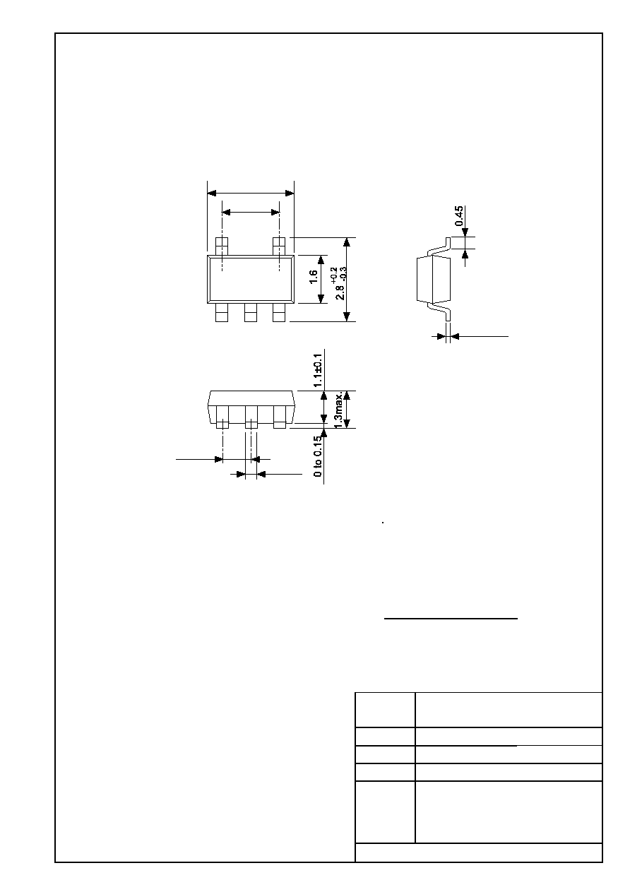
Package
SOT-23-5 (Package drawing code: MP005-A)
EXTERNAL TRANSISTOR TYPE VOLTAGE REGULATOR
S-816 Series
Rev.4.1
_10
2
Seiko Instruments Inc.
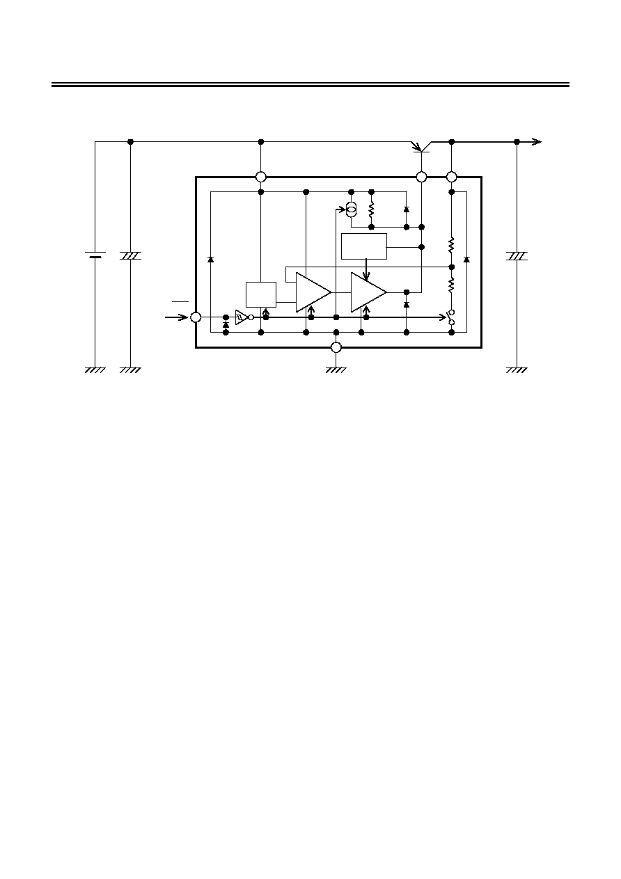
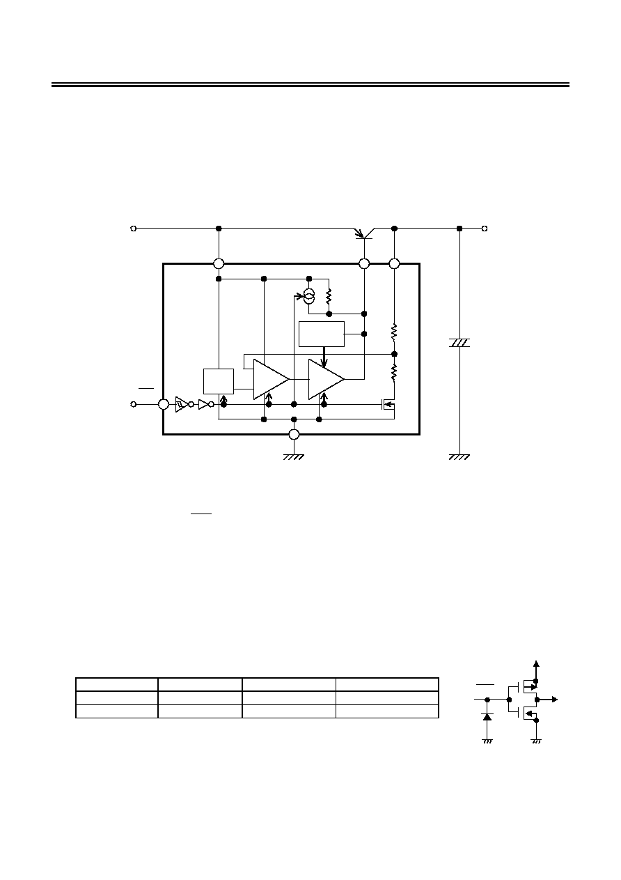
Block Diagram
+
+
+
+
-
-
-
-
EXT VOUT
VSS
OFF
ON/
VIN
V
REF
Current Source
Overcurrent
Protection
Circuit
Pull-Up
Error
Amplifier
Sink
Driver
+
+
+
+
-
-
-
-
+
+
+
+
-
-
-
-
Remark 1. To ensure you power cutoff of the external transistor when the device is powered down, the
EXT output is pulled up to V
IN
by a pull-up resistance (approx. 0.5 M
) inside the IC.
2. The diode inside the IC is a parasitic diode.
Figure 1
EXTERNAL TRANSISTOR TYPE VOLTAGE REGULATOR
Rev.4.1
_10
S-816 Series
Seiko Instruments Inc.
3
Product Code Structure
1. Product Name
S-816A xx A MC - xxx - T2
IC direction in tape specifications
Product name (abbreviation)
Package name (abbreviation)
MC: SOT-23-5
Output voltage
◊ 10
25 to 60 (2.5 V to 6.0 V)
2. Product Name List
Table 1
Output Voltage
(V)
Product Name
Output Voltage
(V)
Product Name
2.5 V
±2.0%
S-816A25AMC-BAA-T2 4.3 V
±2.0%
S-816A43AMC-BAS-T2
2.6 V
±2.0%
S-816A26AMC-BAB-T2 4.4 V
±2.0%
S-816A44AMC-BAT-T2
2.7 V
±2.0%
S-816A27AMC-BAC-T2 4.5 V
±2.0%
S-816A45AMC-BAU-T2
2.8 V
±2.0%
S-816A28AMC-BAD-T2 4.6 V
±2.0%
S-816A46AMC-BAV-T2
2.9 V
±2.0%
S-816A29AMC-BAE-T2 4.7 V
±2.0%
S-816A47AMC-BAW-T2
3.0 V
±2.0%
S-816A30AMC-BAF-T2 4.8 V
±2.0%
S-816A48AMC-BAX-T2
3.1 V
±2.0%
S-816A31AMC-BAG-T2 4.9 V
±2.0%
S-816A49AMC-BAY-T2
3.2 V
±2.0%
S-816A32AMC-BAH-T2 5.0 V
±2.0%
S-816A50AMC-BAZ-T2
3.3 V
±2.0%
S-816A33AMC-BAI-T2 5.1 V
±2.0%
S-816A51AMC-BBA-T2
3.4 V
±2.0%
S-816A34AMC-BAJ-T2 5.2 V
±2.0%
S-816A52AMC-BBB-T2
3.5 V
±2.0%
S-816A35AMC-BAK-T2 5.3 V
±2.0%
S-816A53AMC-BBC-T2
3.6 V
±2.0%
S-816A36AMC-BAL-T2 5.4 V
±2.0%
S-816A54AMC-BBD-T2
3.7 V
±2.0%
S-816A37AMC-BAM-T2 5.5 V
±2.0%
S-816A55AMC-BBE-T2
3.8 V
±2.0%
S-816A38AMC-BAN-T2 5.6 V
±2.0%
S-816A56AMC-BBF-T2
3.9 V
±2.0%
S-816A39AMC-BAO-T2 5.7 V
±2.0%
S-816A57AMC-BBG-T2
4.0 V
±2.0%
S-816A40AMC-BAP-T2 5.8 V
±2.0%
S-816A58AMC-BBH-T2
4.1 V
±2.0%
S-816A41AMC-BAQ-T2 5.9 V
±2.0%
S-816A59AMC-BBI-T2
4.2 V
±2.0%
S-816A42AMC-BAR-T2 6.0 V
±2.0%
S-816A60AMC-BBJ-T2
EXTERNAL TRANSISTOR TYPE VOLTAGE REGULATOR
S-816 Series
Rev.4.1
_10
4
Seiko Instruments Inc.
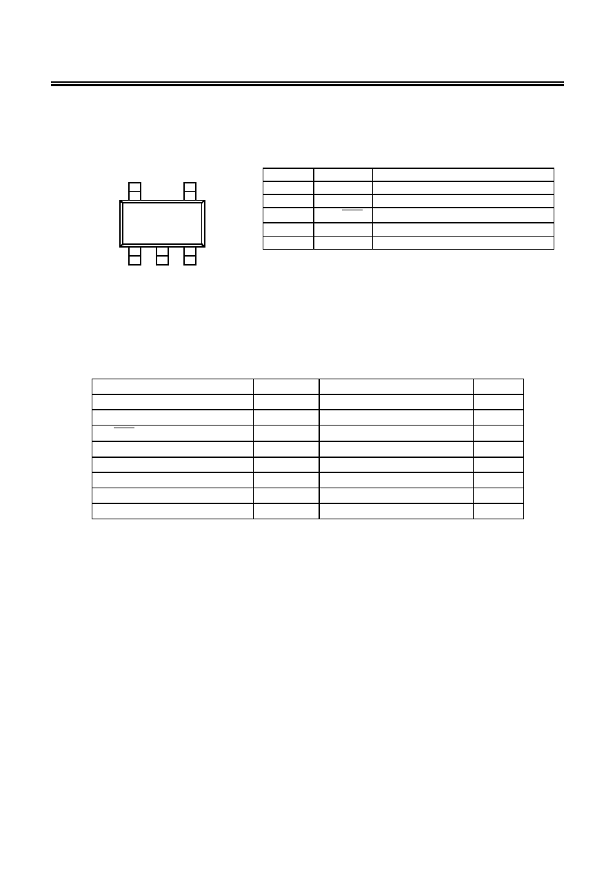
Pin Configuration
Table 2
Pin
No.
Symbol
Description
1
EXT
Output Pin for Base-Current Control
2
VSS
GND
Pin
3
OFF
ON/
Shutdown Pin ("H" active)
4
VIN
IC Power Supply Pin
5
VOUT
Output Voltage Monitoring Pin
SOT-23-5
Top view
1 2 3
5 4
Figure 2
Absolute Maximum Ratings
Table 3
(Ta
=25∞C unless otherwise specified)
Item Symbol
Absolute
Maximum
Ratings
Unit
VIN Pin Voltage
V
IN
V
SS
-0.3 to V
SS
+18
V
VOUT Pin Voltage
V
OUT
V
SS
-0.3 to V
SS
+18
V
OFF
ON/
Pin Voltage
V
ON/OFF
V
SS
-0.3 to V
SS
+18
V
EXT Pin Voltage
V
EXT
V
SS
-0.3 to V
IN
+0.3
V
EXT Pin Current
I
EXT
50
mA
Power Dissipation
P
D
250
mW
Operating Temperature Range
T
opr
-40 to +85
∞C
Storage Temperature Range
T
stg
-40 to +125
∞C
Caution The absolute maximum ratings are rated values exceeding which the product
could suffer physical damage. These values must therefore not be exceeded
under any conditions.

EXTERNAL TRANSISTOR TYPE VOLTAGE REGULATOR
Rev.4.1
_10
S-816 Series
Seiko Instruments Inc.
5
Electrical Characteristics
Table 4
(Ta
=25∞C unless otherwise specified)
Item Symbol
Conditions
Min.
Typ.
Max.
Unit
Test
circuit
Input Voltage
V
IN
16 V 1
Output Voltage
V
OUT
V
IN
=V
OUT
+1 V, I
OUT
=50 mA,
V
ON/OFF
="H"
V
OUT
◊0.98
V
OUT
V
OUT
◊1.02
V 1
Maximum Output Current (PNP
Output)
*1
1
A 1
Drop-Out Voltage
*1
V
drop
I
OUT
=100 mA
100
mV 1
Load Regulation (PNP Output)
*1
V
OUT
V
IN
=V
OUT
+1 V, 1 mA < I
OUT
< 1 A
60 mV 1
Line Regulation (PNP Output)
*1
IN
OUT
OUT
V
V
V
∑
I
OUT
=50 mA, V
OUT
+1 V < V
IN
< 16 V -0.15 0.01 0.15 %/V 1
Output Voltage Temperature
Coefficient
Ta
V
OUT
V
IN
=V
OUT
+1 V, I
OUT
=50 mA,
V
ON/OFF
="H", Ta=-40 to 85∞C
±0.15
mV/∞C 1
Current Consumption during
Operation
I
SS
V
IN
=V
OUT
+1 V, V
ON/OFF
="H"
30 40
µA
1
Current Consumption during
Shutdown
I
STB
V
IN
=16 V, V
ON/OFF
="L"
1
µA
1
EXT Output Source Constant
Current
I
SRC
V
IN
=V
OUT
+1 V, V
ON/OFF
="H",
V
EXT
=V
OUT
, V
OUT
=V
OUT
◊0.95
-10
µA
2
EXT Output Pull-Up Resistance
R
UP
V
IN
=16 V, V
ON/OFF
="L"
0.25 0.50 1.00 M
2
EXT Output Sink Current
I
SINK
V
IN
=V
OUT
+1 V, V
ON/OFF
="H",
V
OUT
=V
OUT
◊0.95
10
mA 2
Leakage Current during EXT
Output Off
I
OFF
V
IN
=V
EXT
=V
OUT
+1 V, V
OUT
=0 V,
V
ON/OFF
="L"
0.1
µA
2
EXT Output Sink Overcurrent
Set Value
I
MAX
V
IN
=V
EXT
=7 V, V
ON/OFF
="H",
V
OUT
=V
OUT
◊0.95
12 16 20 mA 2
Shutdown Pin Input Voltage
V
SH
V
IN
=V
OUT
+1 V, V
OUT
=0 V,
Check V
EXT
="L"
2.4
V 3
V
SL
V
IN
=V
OUT
+1 V, V
OUT
=0 V,
Check V
EXT
="H"
0.3
Shutdown Pin Input Current
I
SH
V
ON/OFF
=V
OUT
+1 V
0.1
µA
2
I
SL
V
ON/OFF
=0 V
-0.1
*1. The characteristics vary with the associated external components.
The characteristics given above are those obtained when the IC is combined with a Toshiba Corporation 2SA1213-Y
for the PNP transistor and a 10
µF tantalum capacitor for the output capacitor (C
L
).
EXTERNAL TRANSISTOR TYPE VOLTAGE REGULATOR
S-816 Series
Rev.4.1
_10
6
Seiko Instruments Inc.
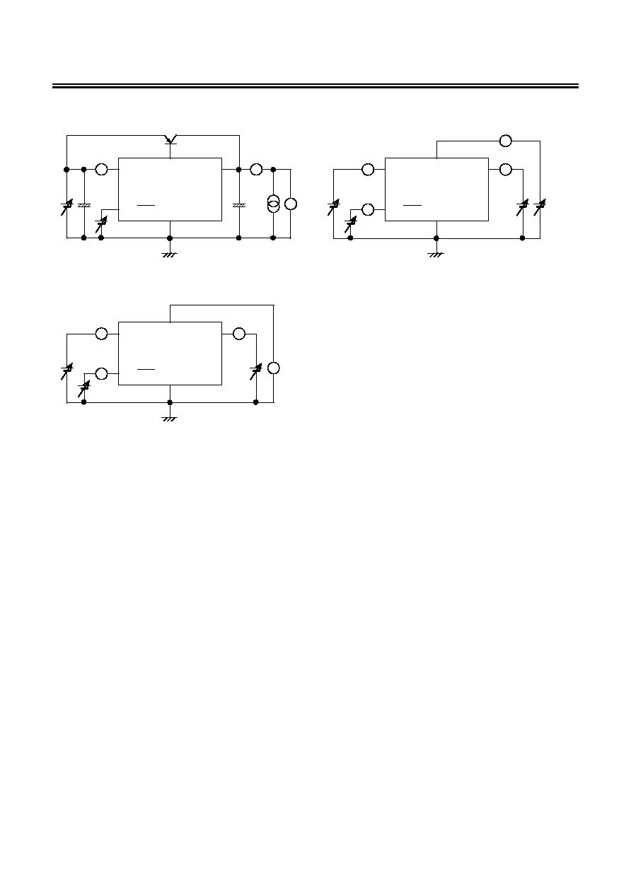
Test Circuits
1.
2.
VIN
EXT VOUT
VSS
OFF
ON/
A
A
V
+
-
+
-
VIN
EXT VOUT
VSS
OFF
ON/
A
A
A
A
Figure 3
Figure 4
3.
VIN
EXT VOUT
VSS
OFF
ON/
A
A
V
A
Figure 5
EXTERNAL TRANSISTOR TYPE VOLTAGE REGULATOR
Rev.4.1
_10
S-816 Series
Seiko Instruments Inc.
7
Operation
1. Basic Operation
Figure 6 shows a block diagram of the S-816 Series.
The device compares the voltage which is obtained from dividing output voltage V
OUT
by feedback
resistances R
A
and R
B
with reference voltage V
REF
through the error amplifier, output of which controls the
sink driver. By regulating the base current of the external PNP transistor, the IC maintains a constant
output voltage that is not susceptible to an input voltage variation or temperature variation.
OUT
IN
C
L
EXT VOUT
VSS
OFF
ON/
VIN
V
REF
Current Source
Overcurrent
Protection
Circuit
R
B
R
A
R
C
Error
Amplifier
Sink
Driver
+
-
+
-
Figure 6
2. Internal Circuits
2.1. Shutdown Pin (
OFF
ON/
Pin)
This pin activates and deactivates the regulating operation.
When the shutdown pin is set to "L", the V
IN
voltage appears through the EXT pin, prodding the external
PNP transistor to off. All the internal circuits stop working, and substantial savings in current consumption
are achieved accordingly. In this condition, the EXT pin is pulled up to V
IN
by a pull-up resistance
(approx. 0.5 M
) inside the IC in order to ensure you power cut off of the external PNP transistor.
The shutdown pin is configured as shown in Figure 7. Since neither pull-up or pull-down is performed
internally, please avoid using the pin in a floating state. Also, be sure to refrain from applying a voltage of
0.3 V to 2.4 V to this pin lest the current consumption increase. When this shutdown pin is not used,
leave it coupled to the VIN pin.
Table 5
Shutdown Pin
Internal Circuit
EXT Pin Voltage
VOUT Pin Voltage
"H" Activated V
IN
-V
BE
Set value
"L" Deactivated V
IN
Hi-Z
VIN
VSS
OFF
ON/
Figure 7

EXTERNAL TRANSISTOR TYPE VOLTAGE REGULATOR
S-816 Series
Rev.4.1
_10
8
Seiko Instruments Inc.
2.2. Overcurrent Protection Circuit
The overcurrent protection function of the S-816 Series monitors the EXT pin sink current (base current of
the external PNP transistor) with an overcurrent protection circuit incorporated in the IC, and limits that
current (EXT pin sink current).
As the load current increases, the EXT pin sink current (base current of the external PNP transistor) also
grows larger to maintain the output voltage. The overcurrent protection circuit clamps and limits the EXT
pin sink current to the EXT output sink overcurrent set value (I
MAX
) in order to prevent it from increasing
beyond that value.
The load current at which the overcurrent protection function works is represented by the following
equation:
I
OUT_MAX
= I
MAX
◊ h
FE
In this case, h
FE
is the DC amplification factor of the external PNP transistor.
I
OUT_MAX
represents the maximum output current of this regulator. If it is attempted to obtain a higher load
current, the output voltage will fall.
Note that within the overcurrent protection function of this IC, the external PNP transistor may not be able
to be protected from collector overcurrents produced by an EXT-GND short-circuiting or other
phenomenon occurring outside the IC. To protect the external PNP transistor from such collector
overcurrents, it will be necessary to choose a transistor with a larger power dissipation than I
OUT_MAX
◊ V
IN
,
or to add an external overcurrent protection circuit. With regard to this external overcurrent protection
circuit, refer to "Overcurrent Protection Circuit" in " Application Circuits".
2.3. Phase Compensation Circuit
The S-816 Series performs phase compensation with a phase compensation circuit, incorporated in the
IC, and the ESR (Equivalent Series Resistance) of an output capacitor, to secure stable operation even in
the presence of output load variation. A uniquely devised phase compensation circuit has resulted in
improved transient response characteristics of the IC, while preserving the same feature of low current
consumption. This feature allows the IC to be used in applications where the input variation or load
variation is heavy.
Because the S-816 Series is designed to perform the phase compensation, utilizing the ESR of an output
capacitor, such output capacitor (C
L
) should always be placed between VOUT and VSS. Since each
capacitor to be employed has an optimum range of their own characteristics, be sure to choose
components for the IC with your all attention. For details, refer to " Selection of Associated External
Components".
EXTERNAL TRANSISTOR TYPE VOLTAGE REGULATOR
Rev.4.1
_10
S-816 Series
Seiko Instruments Inc.
9
Selection of Associated External Components
1. External PNP Transistor
Select an external transistor according to the conditions of input voltage, output voltage, and output
current. A low-saturation voltage PNP transistor with "h
FE
" ranging from 100 to 300 will be suitable for this
IC.
The parameters for selection of the external PNP transistor include the maximum collector-base voltage,
the maximum collector-emitter voltage, the DC amplification factor (h
FE
), the maximum collector current
and the collector dissipation.
The maximum collector-base voltage and the maximum collector-emitter voltage are determined by the
input voltage range in each specific application to be employed. You may select a transistor with an input
voltage at least several volts higher than the expected maximum input voltage.
The DC amplification factor (h
FE
) affects the maximum output current that can be supplied to the load.
With an internal overcurrent protection circuit of this IC, the base current is clamped, and will not exceed
the overcurrent set value (I
MAX
). Select a transistor which is capable of delivering the required maximum
output current to the intended application, with hfe and maximum collector current. (Refer to
" Overcurrent Protection Circuit")
Likewise, select a transistor, based on the maximum output current and the difference between the input
and output voltages, with due attention to the collector dissipation.
2. Output Capacitor (C
L
)
The S-816 Series performs phase compensation by an internal phase compensation circuit of IC, and the
ESR (Equivalent Series Resistance) of an output capacitor for to secure stable operation even in the
presence of output load variation. Therefore, always place a capacitor (C
L
) of 4.7
µF or more between
VOUT and VSS.
For stable operation of the S-816 Series, it is essential to employ a capacitor with an ESR having
optimum range. Whether an ESR is larger or smaller than that optimum range (approximately 0.1
to
5
), this could produce an unstable output, and cause a possibility of oscillations. For this reason, a
tantalum electrolytic capacitor is recommended.
When a ceramic capacitor or an OS capacitor having a low ESR is selected, it will be necessary to
connect an additional resistance that serves for the ESR in series with the output capacitor, as illustrated
in Figure 8. The resistance value that needs to be added will be from 0.1
to 5 , but this value may
vary depends on the service conditions, and should be defined through careful evaluation in advance. In
general, our recommendation is 0.3
or so.
An aluminum electrolytic capacitor tends to produce oscillations as its ESR increases at a low
temperature. Beware of this case. When this type of capacitor is employed, make thorough evaluation of
it, including its temperature characteristics.
OUT
IN
R
0.3
C
L
S-816 Series
EXT VOUT
VSS
OFF
ON/
VIN
Figure 8
Caution The above connection diagram and constant will not guarantee successful operation.
Perform through evaluation using the actual application to set the constant.
EXTERNAL TRANSISTOR TYPE VOLTAGE REGULATOR
S-816 Series
Rev.4.1
_10
10
Seiko Instruments Inc.
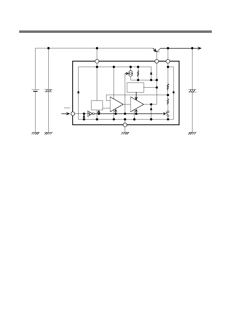
Standard Circuit
+
+
+
+
-
-
-
-
EXT VOUT
VSS
OFF
ON/
VIN
V
REF
Current Source
Overcurrent
Protection
Circuit
Pull-Up
Error
Amplifier
Sink
Driver
+
+
+
+
-
-
-
-
+
+
+
+
-
-
-
-
Figure 9
Caution The above connection diagram does not guarantee correct operation. Perform
sufficient evaluation using the actual application to set the constant.
EXTERNAL TRANSISTOR TYPE VOLTAGE REGULATOR
Rev.4.1
_10
S-816 Series
Seiko Instruments Inc.
11
Precautions
∑ The overcurrent protection function of this IC detects and limits the sink current at the EXT pin inside the
IC. Therefore, it does not work on collector overcurrents which are caused by an EXT-GND short-
circuiting or other phenomenon outside the IC. To protect the external PNP transistor from collector
overcurrents perfectly, it is necessary to provide another external overcurrent protection circuit.
∑ This IC performs phase compensation by using an internal phase compensator circuit and the ESR of an
output capacitor. Therefore, always place a capacitor of 4.7
µF or more between VOUT and VSS.
A tantalum type capacitor is recommended for this purpose. Moreover, to secure stable operation of the
S-816 Series, it will be necessary to employ a capacitor having an ESR (Equivalent Series Resistance)
covered in a certain optimum range (0.1
to 5 ). Whether an ESR is larger or smaller than that
optimum range, this could result in an unstable output, and cause a possibility of oscillations. Select a
capacitor through careful evaluation made according to the actual service conditions.
∑ Do not apply an electrostatic discharge to this IC that exceeds the performance ratings of the built-in
electrostatic protection circuit.
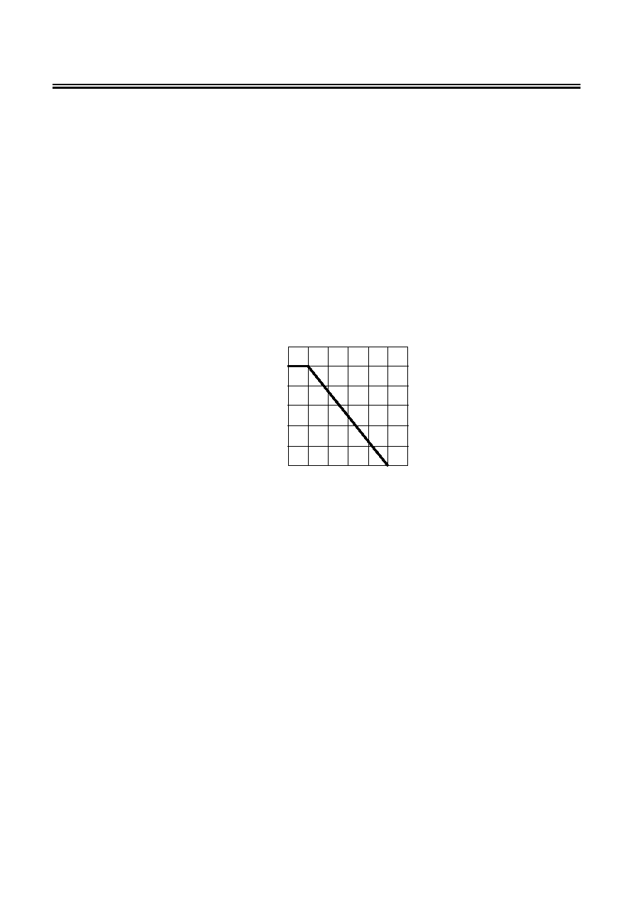
∑ Make sure that the power dissipation inside the IC due to the EXT output sink current (especially at a high
temperature) will not surpass the power dissipation of the package.
150
200
100
0
100
50
0
300
Ambient Temperature Ta (
∞C)
Power
Dissipation
P
D
(mW)
Figure 10 Power Dissipation of SOT-23-5 Package (When Not Mounted)
∑ SII claims no responsibility for any disputes arising out of or in connection with any infringement by
products including this IC of patents owned by a third party.
EXTERNAL TRANSISTOR TYPE VOLTAGE REGULATOR
S-816 Series
Rev.4.1
_10
12
Seiko Instruments Inc.
Application Circuits
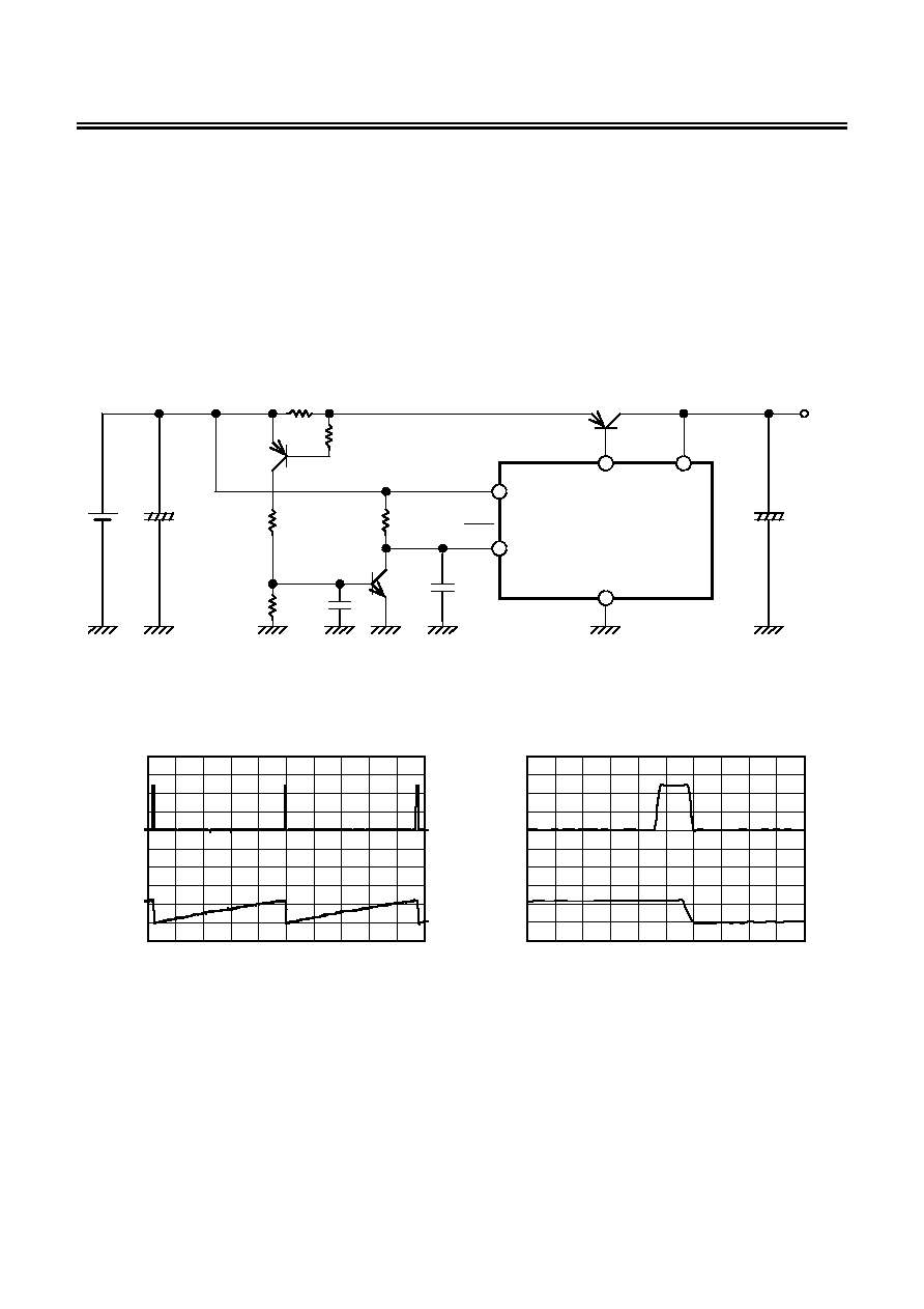
1. Overcurrent Protection Circuit
Figure 11 shows a sample of overcurrent protection implemented with an external circuit connected.
The internal overcurrent protection function of the S-816 Series is designed to detect the sink current
(base current of the PNP transistor) at the EXT pin, therefore it may not be able to protect the external
PNP transistor from collector overcurrents caused by an EXT-GND short-circuiting or other phenomenon
occurring outside the IC.
This sample circuit activates the regulator intermittently against collector overcurrents, thereby
suppressing the heat generation of the external PNP transistor.
The duty of the on-time and off-time of the intermittent operation can be regulated through an external
component.
V
IN
C
IN
10
µF
+
-
R
2
2 k
R
1
100 k
R
S
0.5
R
4
2 k
Tr1
R
3
2 k
C
2
0.22
µF
Tr2 C
1
0.22
µF
C
L
10
µF
+
-
VIN
EXT VOUT
S-816 Series
VSS
OUT
OFF
ON/
2SA1213Y
Figure 11
Caution The above connection diagram and constant will not guarantee successful operation.
Perform through evaluation using the actual application to set the constant.
S-816A30AMC (V
IN
=4 V)
1 A
Load Current
(0.5 A/div)
0 A
2 V
V
ON/OFF
(1 V/div)
0 V
t (2 ms/div)
S-816A30AMC (V
IN
=4 V)
1 A
Load Current
(0.5 A/div)
0 A
2 V
V
ON/OFF
(1 V/div)
0 V
t (100
µs/div)
Figure 12 Output Current Waveforms during Intermittent Operation Prompted by Load Short-Circuiting
The detection of the overcurrent is done by the sense resistance (R
S
) and the PNP transistor (Tr1).
When Tr1 comes on, triggered by a voltage drop of R
S
, the NPN transistor (Tr2) also comes on, according
to the time constants of the capacitor (C
2
) and resistance (R
2
). This causes the shutdown pin to turn to
the "L" level, and the regulating operation to stop, and interrupting the current to the load.
When the load current is cut off, the voltage drop of R
S
stops. This makes Tr1 off again, and also makes
the NPN transistor (Tr2) off.
In this condition, the shutdown pin returns to the "H" level, according to the time constants of the
capacitor (C
1
) and resistance (R
1
). This delay time in which shutdown pin returns to the "H" level from the
"L" level is the time in which the load current remains cut off.
EXTERNAL TRANSISTOR TYPE VOLTAGE REGULATOR
Rev.4.1
_10
S-816 Series
Seiko Instruments Inc.
13
If an overcurrent flows again after the shutdown pin has assumed the "H" level following the delay time
and the regulating operation has been restarted, the circuit will again suspend the regulating operation
and resume the intermittent operation. This intermittent operation will be continued till the overcurrentt is
eliminated, and once theovercurrent disappears, the normal operation will be restored.
The overcurrent detection value (I
OUT_MAX
) is represented by the following equation:
I
OUT_MAX
= |V
BE1
| / R
S
In this case, R
S
denotes the resistance value of the sense resistance, and V
BE1
denotes the base-emitter
saturation voltage of Tr1.
For the PNP transistor (Tr1) and the NPN transistor (Tr2), try to select those of small-signal type that offer
a sufficient withstand voltage against the input voltage (V
IN
).
The on-time (t
ON
) and the off-time (t
OFF
) of the intermittent operation are broadly expressed by the
following equations:
t
ON
= -1 ◊ C
2
◊ R
2
◊ L
N
( 1
- ( V
BE2
◊ ( 1 + R
2
/ R
3
) ) / ( V
IN
- V
BE1
) )
t
OFF
= -1 ◊ C
1
◊ R
1
◊ L
N
( 1
- V
SH
/ V
IN
)
In this case, V
BE2
denotes the base-emitter saturation voltage of Tr2, V
IN
denotes the input voltage, and
V
SH
denotes the inversion voltage ("L"
"H") of the shutdown pin.
Set the on-time value that does not cause the overcurrent protection to be activated by a rush current to
the load capacitor. Then, compute the ratio between the on-time and the off-time from the maximum
input voltage of the appropriate application and the power dissipation of the external PNP transistor, and
decide the off-time with reference to the on-time established earlier.
Take the equation above as a rough guide, because the actual on-time (t
ON
) and off-time (t
OFF
) should be
defined and checked using the utilizing components.
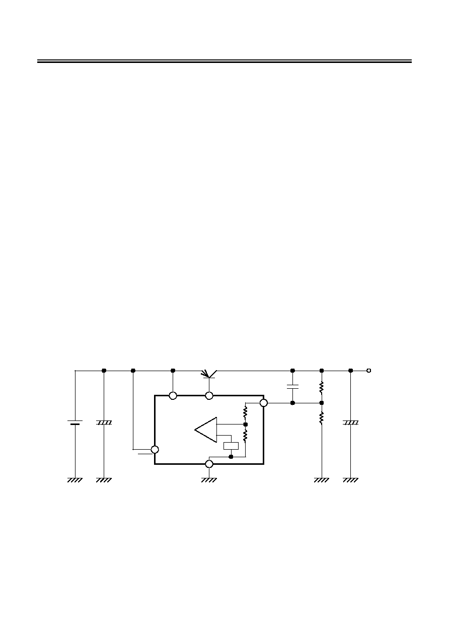
2. External Adjustment of Output Voltage
The S-816 Series allows you to adjust the output voltage or to set its value over the output voltage range
(6 V) of the products of this series, when external resistances R
A
, R
B
and capacitor C
C
are added, as
illustrated in Figure 13. Moreover, a temperature gradient can be obtained by inserting a thermistor or
other element in series with external resistances R
A
and R
B
.
V
IN
C
IN
+
-
C
L
OFF
ON/
VIN EXT
+
-
VOUT
VSS
OUT
+
-
C
C
R
A
R
B
R
1
R
2
Error
amplifier
V
REF
Figure 13
The S-816 Series has an internal impedance resulting from R
1
and R
2
between the VOUT and the VSS
pin, as shown in Figure 13. Therefore, the influence of the internal resistances (R
1
, R
2
) of the IC has to
be taken into consideration in defining the output voltage (OUT).
The output voltage (OUT) is expressed by the following equation:
OUT
= V
OUT
+ V
OUT
◊ R
A
˜ ( R
B
//
*1
R
I
)
*1. "//" denotes a combined resistance in parallel.
In this case, V
OUT
is the output voltage value of the S-816 Series, R
A
and R
B
is the resistance values of
the external resistances, and R
I
is the resistance value (R
1
+R
2
) of the internal resistances in the IC.

EXTERNAL TRANSISTOR TYPE VOLTAGE REGULATOR
S-816 Series
Rev.4.1
_10
14
Seiko Instruments Inc.
The accuracy of the output voltage (OUT) is determined by the absolute accuracy of external connecting
resistances R
A
and R
B
, the output voltage accuracy (V
OUT
±2.0%) of the S-816 Series, and deviations in
the absolute value of the internal resistance (R
I
) in the IC.
The maximum value (OUTmax) and the minimum value (OUTmin) of the output voltage (OUT), including
deviations, are expressed by the following equations:
OUTmax
= V
OUT
◊ 1.02 + V
OUT
◊ 1.02 ◊ R
Amax
˜ ( R
Bmin
// R
Imin
)
OUTmin
= V
OUT
◊ 0.98 + V
OUT
◊ 0.98 ◊ R
Amin
˜ ( R
Bmax
// R
Imax
)
Where R
Amax
, R
Amin
, R
Bmax
and R
Bmin
denote the maximum and minimum of the absolute accuracy of
external resistances R
A
and R
B
, and R
Imax
and R
Imin
denote the maximum and minimum deviations of the
absolute value of the internal resistance (R
I
) in the IC, respectively.
The deviations in the absolute value of internal resistance (R
I
) in the IC vary with the output voltage set
value of the S-816 Series, and are broadly classified as follows:
∑ Output voltage (V
OUT
) 2.5 V to 2.7 V
3.29 M to 21.78 M
∑ Output voltage (V
OUT
) 2.8 V to 3.1 V
3.29 M to 20.06 M
∑ Output voltage (V
OUT
) 3.2 V to 3.7 V
2.23 M to 18.33 M
∑ Output voltage (V
OUT
) 3.8 V to 5.1 V
2.23 M to 16.61 M
∑ Output voltage (V
OUT
) 5.2 V to 6.0 V
2.25 M to 14.18 M
If a value of R
I
given by the equation shown below is taken in calculating the output voltage (OUT), a
median voltage deviation of the output voltage (OUT) will be obtained.
R
I
= 2 ˜ ( 1 ˜ (Maximum value of internal resistance of IC) + 1 ˜ (Minimum value of internal resistance of IC) )
The closer the output voltage (OUT) and the output voltage set value (V
OUT
) of the IC are brought to each
other, the more the accuracy of the output voltage (OUT) remains immune to deviations in the absolute
accuracy of external resistances (R
A
, R
B
) and the absolute value of the internal resistance (R
I
) of the IC.
In particular, to suppress the influence of deviations in the internal resistance (R
I
), the resistance values
of external resistances (R
A
, R
B
) need to be limited to a much smaller value than that of the internal
resistance (R
I
). However, since reactive current flows through the external resistances (R
A
, R
B
), there is a
tradeoff between the accuracy of the output voltage (OUT) and the reactive current. This should be taken
into consideration, according to the requirements of the intended application.
Note that when larger value (more than 1 M
) is taken for the external resistances (R
A
, R
B
), IC is
vulnerable to external noise. Check the influence of this value well with the actual application.
Furthermore, add a capacitor C
C
in parallel to the external resistance R
A
in order to avoid output
oscillations and other types of instability. (Refer to Figure 13)
Make sure that the capacitance value of C
C
is larger than the value given by the following equation:
C
C
[F]
1 ˜ ( 2 ◊ ◊ R
A
[
] ◊ 6000 )
Caution The above connection diagram and constant will not guarantee successful operation.
Perform through evaluation using the actual application to set the constant.

EXTERNAL TRANSISTOR TYPE VOLTAGE REGULATOR
Rev.4.1
_10
S-816 Series
Seiko Instruments Inc.
15
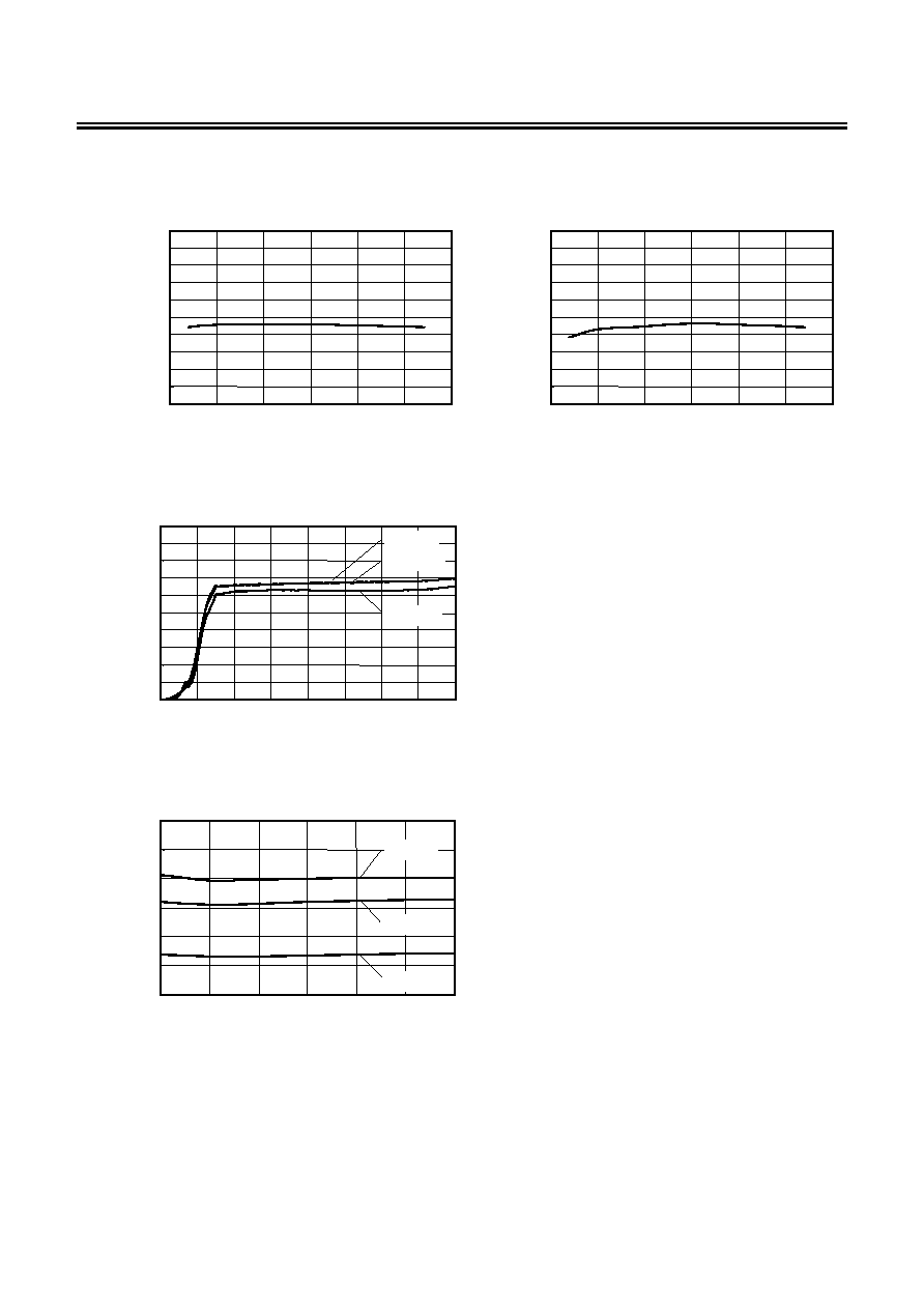
Typical Characteristics
1. Input Voltage (V
IN
) - Output Voltage (V
OUT
) Characteristics
V
IN
-V
OUT
S-816A30AMC (I
OUT
=50 mA)
V
IN
-V
OUT
S-816A50AMC (I
OUT
=50 mA)
Ta
=-40∞C
Ta
=85∞C
Ta
=25∞C
3.10
3.08
3.06
3.04
3.02
3.00
2.98
2.96
2.94
2.92
2.90
2 4 6 8 10
12
14
16
V
IN
(V)
V
OUT
(V)
Ta
=85∞C
Ta
=-40∞C
Ta
=25∞C
5.10
5.08
5.06
5.04
5.02
5.00
4.98
4.96
4.94
4.92
4.90
2 4 6 8 10
12
14
16
V
IN
(V)
V
OUT
(V)
V
IN
-V
OUT
S-816A30AMC (Ta
=25∞C)
V
IN
-V
OUT
S-816A50AMC (Ta
=25∞C)
I
OUT
=1 mA
I
OUT
=100 mA
I
OUT
=500 mA
I
OUT
=1 A
3.10
3.05
3.00
2.95
2.90
2.85
2.80
2.8 2.9 3.0 3.1 3.2 3.3 3.4 3.5 3.6 3.7 3.8
V
IN
(V)
V
OUT
(V)
I
OUT
=1 A
I
OUT
=1 mA
I
OUT
=100 mA
I
OUT
=500 mA
5.10
5.05
5.00
4.95
4.90
4.85
4.80
4.8 4.9 5.0 5.1 5.2 5.3 5.4 5.5 5.6 5.7 5.8
V
IN
(V)
V
OUT
(V)
2. Output Current (I
OUT
) - Output Voltage (V
OUT
) Characteristics
I
OUT
-V
OUT
S-816A30AMC (V
IN
=4 V)
I
OUT
-V
OUT
S-816A50AMC (V
IN
=6 V)
Ta
=85∞C
Ta
=25∞C
Ta
=-40∞C
3.10
3.08
3.06
3.04
3.02
3.00
2.98
2.96
2.94
2.92
2.90
1 10
100
1000
I
OUT
(mA)
V
OUT
(V)
Ta
=25∞C
Ta
=85∞C
Ta
=-40∞C
5.10
5.08
5.06
5.04
5.02
5.00
4.98
4.96
4.94
4.92
4.90
1 10
100
1000
I
OUT
(mA)
V
OUT
(V)
EXTERNAL TRANSISTOR TYPE VOLTAGE REGULATOR
S-816 Series
Rev.4.1
_10
16
Seiko Instruments Inc.
3. Temperature (Ta) - Output Voltage (V
OUT
) Characteristics
Ta-V
OUT
S-816A30AMC (V
IN
=4 V, I
OUT
=50 mA)
Ta-V
OUT
S-816A50AMC (V
IN
=6 V, I
OUT
=50 mA)
3.10
3.08
3.06
3.04
3.02
3.00
2.98
2.96
2.94
2.92
2.90
-50
-25 0 25 50 75 100
Ta (
∞C)
V
OUT
(V)
5.10
5.08
5.06
5.04
5.02
5.00
4.98
4.96
4.94
4.92
4.90
-50
-25 0 25 50 75 100
Ta (
∞C)
V
OUT
(V)
4. Input Voltage (V
IN
) - Consumption Current (I
SS
) Characteristics
V
IN
-I
SS
S-816A30AMC (V
ON/OFF
="H")
Ta
=-40∞C
Ta
=85∞C
Ta
=25∞C
50
45
40
35
30
25
20
15
10
5
0
0 2 4 6 8 10 12
14
16
V
IN
(V)
I
SS
(
µA)
5. Input Voltage (V
IN
) - EXT Output Sink Overcurrent Set Value (I
MAX
) Characteristics
V
IN
-I
MAX
S-816A30AMC
Ta
=-40∞C
Ta
=85∞C
Ta
=25∞C
22
20
18
16
14
12
10
4 6 8 10
12
14
16
V
IN
(V)
I
MAX
(mA)

EXTERNAL TRANSISTOR TYPE VOLTAGE REGULATOR
Rev.4.1
_10
S-816 Series
Seiko Instruments Inc.
17
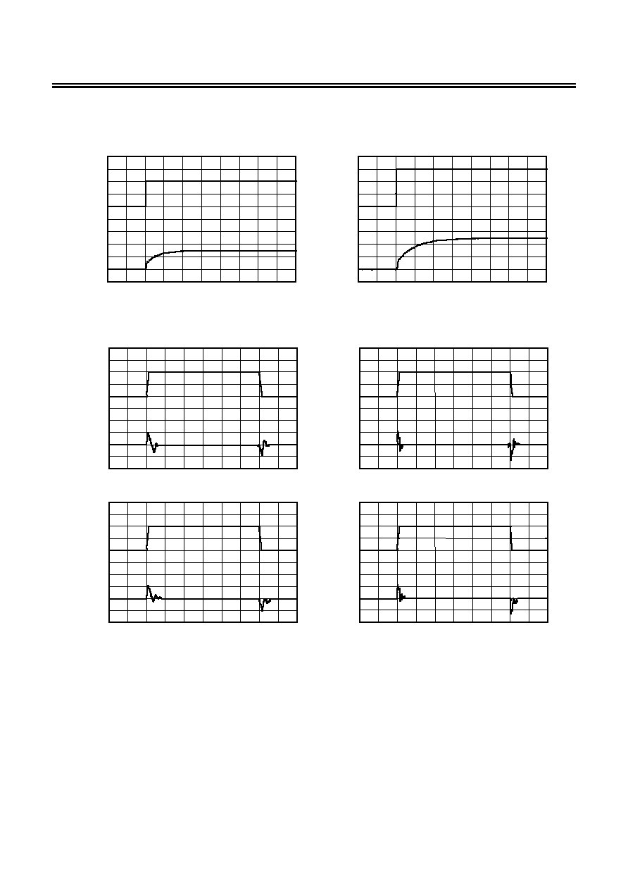
6. Input Voltage (V
IN
) - Shutdown Pin Input Voltage (V
SH
, V
SL
) Characteristics
V
IN
-V
SH
S-816A30AMC
V
IN
-V
SL
S-816A30AMC
Ta
=-40∞C
Ta
=85∞C
Ta
=25∞C
2.5
2.0
1.5
1.0
0.5
0.0
4 6 8 10
12 14
16
V
IN
(V)
V
SH
(V)
Ta
=-40∞C
Ta
=85∞C
Ta
=25∞C
2.5
2.0
1.5
1.0
0.5
0.0
4 6 8 10
12 14
16
V
IN
(V)
V
SL
(V)
EXTERNAL TRANSISTOR TYPE VOLTAGE REGULATOR
S-816 Series
Rev.4.1
_10
18
Seiko Instruments Inc.
Transient Response Characteristics (Typical Data)
1. Input Transient Response Characteristics (Power-on V
IN
=
=
=
=0 V
V
OUT
+
+
+
+1 V, I
OUT
=
=
=
=0 A, C
L
=
=
=
=10 µµµµF)
S-816A30AMC (V
IN
=0 V 4 V)
4 V
V
IN
(2 V/div)
0 V
V
OUT
(2 V/div)
0 V
t (100
µs/div)
S-816A50AMC (V
IN
=0 V 6 V)
6 V
V
IN
(2 V/div)
0 V
V
OUT
(2 V/div)
0 V
t (100
µs/div)
2. Input Transient Response Characteristics (Supply voltage variation V
IN
=
=
=
=V
OUT
+
+
+
+1 V
V
OUT
+
+
+
+2 V, C
L
=
=
=
=10 µµµµF)
S-816A30AMC (I
OUT
=10 mA)
5 V
V
IN
(0.5 V/div)
4 V
V
OUT
(20 mV/div)
3 V
t (100
µs/div)
S-816A30AMC (I
OUT
=300 mA)
5 V
V
IN
(0.5 V/div)
4 V
V
OUT
(20 mV/div)
3 V
t (100
µs/div)
S-816A50AMC (I
OUT
=10 mA)
7 V
V
IN
(0.5 V/div)
6 V
V
OUT
(20 mV/div)
5 V
t (100
µs/div)
S-816A50AMC (I
OUT
=300 mA)
7 V
V
IN
(0.5 V/div)
6 V
V
OUT
(20 mV/div)
5 V
t (100
µs/div)
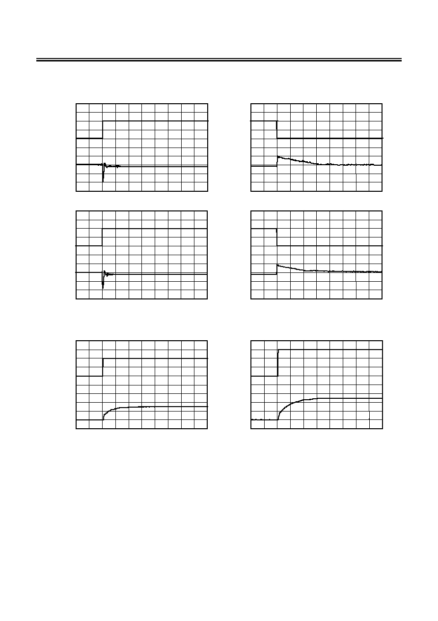
EXTERNAL TRANSISTOR TYPE VOLTAGE REGULATOR
Rev.4.1
_10
S-816 Series
Seiko Instruments Inc.
19
3. Load Transient Response Characteristics (Power-on I
OUT
=
=
=
=1 mA
100 mA, C
L
=
=
=
=10 µµµµF)
S-816A30AMC (V
IN
=4 V)
100 mA
I
OUT
(50 mA/div)
1 mA
V
OUT
(20 mV/div)
3 V
t (50
µs/div)
S-816A30AMC (V
IN
=4 V)
100 mA
I
OUT
(50 mA/div)
1 mA
V
OUT
(20 mV/div)
3 V
t (50
µs/div)
S-816A50AMC (V
IN
=6 V)
100 mA
I
OUT
(50 mA/div)
1 mA
V
OUT
(20 mV/div)
5 V
t (50
µs/div)
S-816A50AMC (V
IN
=6 V)
100 mA
I
OUT
(50 mA/div)
1 mA
V
OUT
(20 mV/div)
5 V
t (50
µs/div)
4. Shutdown Pin Transient Response Characteristics (V
ON/OFF
=
=
=
=0 V
V
IN
, I
OUT
=
=
=
=0 A, C
L
=
=
=
=10 µµµµF)
S-816A30AMC (V
IN
=4 V)
4 V
V
ON/OFF
(2 V/div)
0 V
V
OUT
(2 V/div)
0 V
t (100
µs/div)
S-816A50AMC (V
IN
=6 V)
6 V
V
ON/OFF
(2 V/div)
0 V
V
OUT
(2 V/div)
0 V
t (100
µs/div)
No.
TITLE
SCALE
UNIT
mm
Seiko Instruments Inc.
2.9±0.2
1.9±0.2
0.95±0.1
0.4±0.1
0.16
+0.1
-0.06
1
2
3
4
5
No. MP005-A-P-SD-1.2
MP005-A-P-SD-1.2
SOT235-A-PKG Dimensions
No.
TITLE
SCALE
UNIT
mm
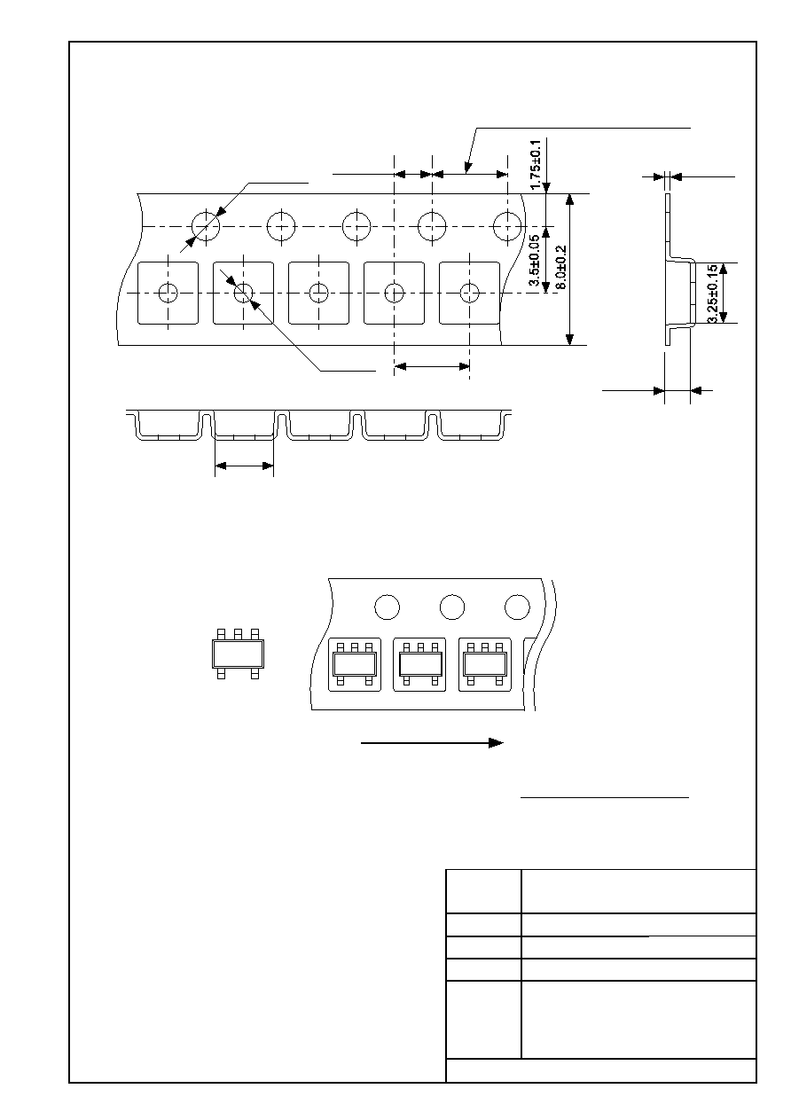
Seiko Instruments Inc.
¯1.5
+0.1
-0
2.0±0.05
¯1.0
+0.2
-0
4.0±0.1
1.4±0.2
0.25±0.1
3.2±0.2
1
2
3
4
5
No. MP005-A-C-SD-2.1
MP005-A-C-SD-2.1
SOT235-A-Carrier Tape
Feed direction
4.0±0.1(10 pitches:40.0±0.2)
No.
TITLE
SCALE
UNIT
mm
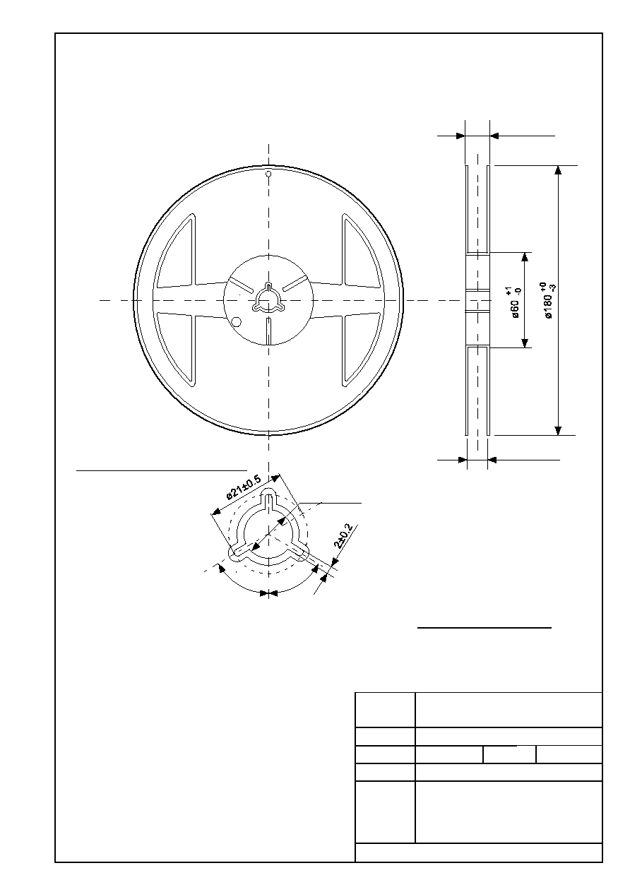
Seiko Instruments Inc.
12.5max.
9.0±0.3
¯13±0.2
(60∞)
(60∞)
QTY.
3,000
No. MP005-A-R-SD-1.1
MP005-A-R-SD-1.1
SOT235-A-Reel
Enlarged drawing in the central part

∑
The information described herein is subject to change without notice.
∑
Seiko Instruments Inc. is not responsible for any problems caused by circuits or diagrams described herein
whose related industrial properties, patents, or other rights belong to third parties. The application circuit
examples explain typical applications of the products, and do not guarantee the success of any specific
mass-production design.
∑
When the products described herein are regulated products subject to the Wassenaar Arrangement or other
agreements, they may not be exported without authorization from the appropriate governmental authority.
∑
Use of the information described herein for other purposes and/or reproduction or copying without the
express permission of Seiko Instruments Inc. is strictly prohibited.
∑
The products described herein cannot be used as part of any device or equipment affecting the human
body, such as exercise equipment, medical equipment, security systems, gas equipment, or any apparatus
installed in airplanes and other vehicles, without prior written permission of Seiko Instruments Inc.
∑
Although Seiko Instruments Inc. exerts the greatest possible effort to ensure high quality and reliability, the
failure or malfunction of semiconductor products may occur. The user of these products should therefore
give thorough consideration to safety design, including redundancy, fire-prevention measures, and
malfunction prevention, to prevent any accidents, fires, or community damage that may ensue.