 | –≠–ª–µ–∫—Ç—Ä–æ–Ω–Ω—ã–π –∫–æ–º–ø–æ–Ω–µ–Ω—Ç: S-817B30A | –°–∫–∞—á–∞—Ç—å:  PDF PDF  ZIP ZIP |
Document Outline
- S-817 Series
- Cover
- Features
- Applications
- Package
- Block Diagrams
- Product Code Structure
- Pin Configuration
- Absolute Maximum Ratings
- Electrical Characteristics
- Test Circuits
- Standard Circuit
- Technical Terms
- Operation
- Selection of Output Capacitor (CL)
- Application Circuits
- Precautions
- Typical Operating Characteristics
- Transient Response Charcteristics (Typical data:Ta =25 ∞C)
- Package Drawing
- SC-82AB
- SOT-23-5
- SOT-89-3
- TO-92 (Bulk)
- TO-92 (Tape and reel)
- TO-92 (Tape and ammo)
Rev.2.4
_00
SUPER-SMALL PACKAGE CMOS VOLTAGE REGULATOR
S-817 Series
Seiko Instruments Inc.
1
The S-817 is an ultra compact 3-Pin positive voltage
regulator developed using CMOS technology.
Housing into a miniaturized 2.0
◊ 2.1 mm SC-82AB
package, the S-817 offers key advantages for small,
portable applications.
The S-817 allows many types of output capacitors
including ceramic capacitors and ensures highly-
stable operations at light load as low as 1
µA.
Features
∑ Ultra-low current consumption: Operating current: Typ. 1.2 µA, Max. 2.5 µA
∑ Output voltage:
1.1 to 6.0 V, selectable in 0.1 V steps.
∑ Output voltage accuracy:
±2.0%
∑ Output current:
50 mA capable (3.0 V output product, V
IN
=5 V)
*1
75 mA capable (5.0 V output product, V
IN
=7 V)
*1
∑ Dropout voltage:
Typ. 160 mV (V
OUT
= 5.0 V, I
OUT
= 10 mA)
∑ Low ESR capacitor (e.g., a ceramic capacitor of 0.1 µF or more) can be used as an output capacitor.
∑ Short circuit protection for:
Series A
∑ Excellent Line Regulation:
Stable operation at light load of 1
µA
*1. Attention should be paid to the power dissipation of the package when the output current is large.
Applications
∑ Power source for battery-powered devices
∑ Power source for personal communication devices
∑ Power source for home electric/electronic appliances
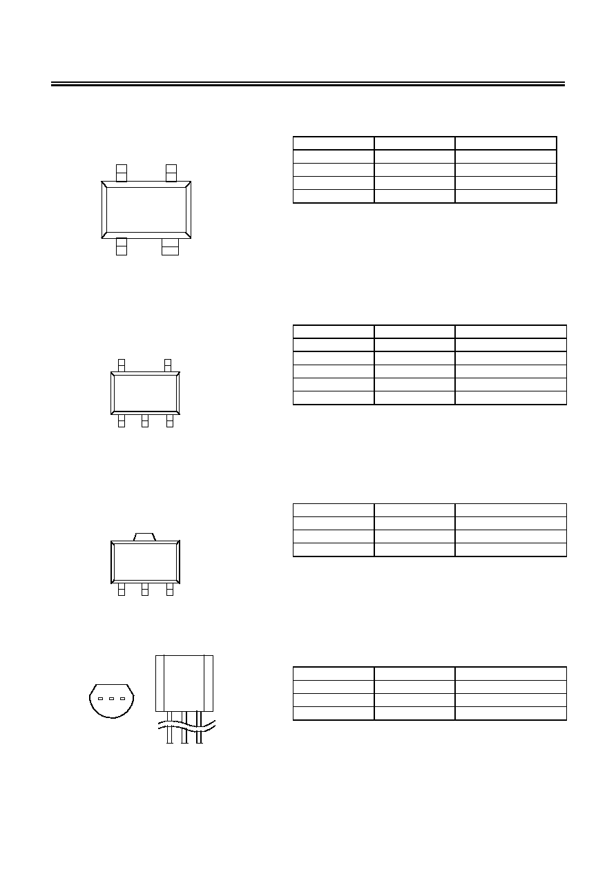
Package
Package name
Drawing code
Package
Tape
Reel
Zigzag
SC-82AB
NP004-A NP004-A NP004-A
SOT-23-5
MP005-A MP005-A MP005-A
SOT-89-3
UP003-A UP003-A UP003-A
TO-92 (Bulk)
YS003-B
TO-92 (Tape and reel)
YF003-A
YF003-A
YF003-A
TO-92 (Tape and ammo)
YF003-A
YZ003-C
YZ003-C

SUPER-SMALL PACKAGE CMOS VOLTAGE REGULATOR
S-817 Series
Rev.2.4
_00
2
Seiko Instruments Inc.
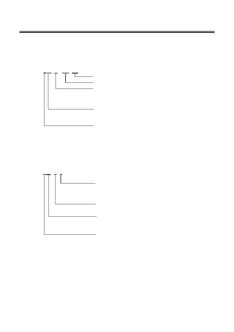
Block Diagrams
1. S-817A Series
Reference
voltage
VSS
VOUT
VIN
*1
Short circuit
protection
*2
+
-
*1. Parasitic diode
Figure 1
2. S-817B Series
Reference
voltage
VSS
VOUT
VIN
*1
+
-
*1. Parasitic diode
Figure 2
SUPER-SMALL PACKAGE CMOS VOLTAGE REGULATOR
Rev.2.4
_00
S-817 Series
Seiko Instruments Inc.
3
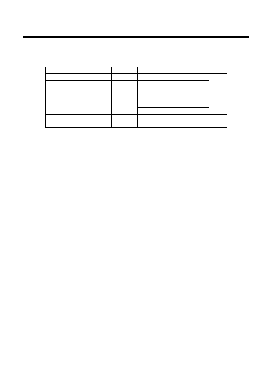
Product Code Structure
1. Product name
1.1 Package SC-82A, SOT-23-5 & SOT-89-3
S-817x xx Axx - xxx - T2
IC direction in tape specifications
*1
Package name (abbreviation)
*2
NB: SC-82AB
MC: SOT-23-5
UA: SOT-89-3
Product name (abbreviation)
Short circuit protection
A
= Yes
B
= No
Output voltage
11 to 60
(E.g., when the output voltage is 1.5 V, it is expressed 15)
*1. Refer to the specifications at the end of this book.
*2. Refer to the "Product name list".
1.2 Package TO-92
S-817x xx AY - x
Package name (abbreviation)
*1
Y: TO-92
Product name (abbreviation)
B: Bulk
Z: Tape and ammo
T: Tape and Reel
Short circuit protection
A
= Yes
B
= No
Output voltage
11 to 60
(E.g., when the output voltage is 1.5 V, it is expressed 15)
*1. Refer to the "Product name list".
SUPER-SMALL PACKAGE CMOS VOLTAGE REGULATOR
S-817 Series
Rev.2.4
_00
4
Seiko Instruments Inc.
2. Product name list
2.1 S-817A series
Table 1
Output voltage
SC-82AB
SOT-23-5
1.1 V
±2.0 %
S-817A11ANB-CUA-T2
1.2 V
±2.0 %
S-817A12ANB-CUB-T2
1.3 V
±2.0 %
S-817A13ANB-CUC-T2
1.4 V
±2.0 %
S-817A14ANB-CUD-T2 S-817A14AMC-T2
1.5 V
±2.0 %
S-817A15ANB-CUE-T2
1.6 V
±2.0 %
S-817A16ANB-CUF-T2 S-817A16AMC-T2
1.7 V
±2.0 %
1.8 V
±2.0 %
S-817A18ANB-CUH-T2
1.9 V
±2.0 %
S-817A19ANB-CUI-T2
2.0 V
±2.0 %
S-817A20ANB-CUJ-T2
2.1 V
±2.0 %
S-817A21ANB-CUK-T2
2.2 V
±2.0 %
S-817A22ANB-CUL-T2
2.4 V
±2.0 %
S-817A24ANB-CUN-T2
2.5 V
±2.0 %
S-817A25ANB-CUO-T2
2.6 V
± 2.0 %
S-817A26ANB-CUP-T2
2.7 V
±2.0 %
S-817A27ANB-CUQ-T2
2.8 V
±2.0 %
S-817A28ANB-CUR-T2
2.9 V
±2.0 %
S-817A29ANB-CUS-T2
3.0 V
±2.0 %
S-817A30ANB-CUT-T2
3.2 V
±2.0 %
S-817A32ANB-CUV-T2
3.3 V
±2.0 %
S-817A33ANB-CUW-T2
3.4 V
±2.0 %
3.5 V
±2.0 %
S-817A35ANB-CUY-T2
3.6 V
±2.0 %
S-817A36ANB-CUZ-T2
3.7 V
±2.0 %
S-817A37ANB-CVA-T2
3.8 V
±2.0 %
4.0 V
±2.0 %
S-817A40ANB-CVD-T2
4.2 V
±2.0 %
S-817A42ANB-CVF-T2
4.3 V
±2.0 %
S-817A43ANB-CVG-T2
4.5 V
±2.0 %
S-817A45ANB-CVI-T2
4.8 V
±2.0 %
S-817A48ANB-CVL-T2
5.0 V
±2.0 %
S-817A50ANB-CVN-T2
5.2 V
± 2.0 %
5.3 V
±2.0 %
5.6 V
±2.0 %
S-817A56ANB-CVT-T2
6.0 V
±2.0 %
Remark Please contact the SII marketing department for products with an output voltage
over than those specified above.
SUPER-SMALL PACKAGE CMOS VOLTAGE REGULATOR
Rev.2.4
_00
S-817 Series
Seiko Instruments Inc.
5
2.2 S-817B series
Table 2
Output voltage
SOT-23-5
SOT-89-3
TO-92
*1
1.1 V
±2.0 %
S-817B11AMC-CWA-T2 S-817B11AUA-CWA-T2 S-817B11AY-x
1.2 V
±2.0 %
S-817B12AMC-CWB-T2 S-817B12AUA-CWB-T2
1.3 V
±2.0 %
S-817B13AMC-CWC-T2
1.5 V
±2.0 %
S-817B15AMC-CWE-T2 S-817B15AUA-CWE-T2 S-817B15AY-x
1.6 V
±2.0 %
S-817B16AMC-CWF-T2 S-817B16AUA-CWF-T2
1.7 V
±2.0 %
S-817B17AMC-CWG-T2
1.8 V
±2.0 %
S-817B18AMC-CWH-T2 S-817B18AUA-CWH-T2
1.9 V
±2.0 %
S-817B19AUA-CWI-T2
2.0 V
±2.0 %
S-817B20AMC-CWJ-T2 S-817B20AUA-CWJ-T2
2.2 V
±2.0 %
S-817B22AMC-CWL-T2
2.5 V
±2.0 %
S-817B25AMC-CWO-T2 S-817B25AUA-CWO-T2 S-817B25AY-x
2.7 V
±2.0 %
S-817B27AUA-CWQ-T2
2.8 V
±2.0 %
S-817B28AMC-CWR-T2
3.0 V
±2.0 %
S-817B30AMC-CWT-T2 S-817B30AUA-CWT-T2 S-817B30AY-x
3.3 V
±2.0 %
S-817B33AMC-CWW-T2 S-817B33AUA-CWW-T2 S-817B33AY-x
3.5 V
±2.0 %
S-817B35AMC-CWY-T2 S-817B35AUA-CWY-T2
3.6 V
±2.0 %
S-817B36AUA-CWZ-T2
3.7 V
±2.0 %
S-817B37AMC-CXA-T2 S-817B37AUA-CXA-T2 S-817B37AY-x
3.8 V
±2.0 %
S-817B38AMC-CXB-T2 S-817B38AUA-CXB-T2
4.0 V
±2.0 %
S-817B40AMC-CXD-T2 S-817B40AUA-CXD-T2 S-817B40AY-x
4.2 V
±2.0 %
S-817B42AMC-CXF-T2
4.3 V
±2.0 %
S-817B43AUA-CXG-T2
4.5 V
±2.0 %
S-817B45AUA-CXI-T2
5.0 V
±2.0 %
S-817B50AMC-CXN-T2 S-817B50AUA-CXN-T2 S-817B50AY-x
5.2 V
±2.0 %
S-817B52AUA-CXP-T2 S-817B52AY-x
5.3 V
±2.0 %
S-817B53AUA-CXQ-T2
5.6 V
±2.0 %
S-817B56AUA-CXT-T2
6.0 V
±2.0 %
S-817B60AUA-CXX-T2 S-817B60AY-x
*1. X changes according to the packing form in TO-92. Standard forms are B; Bulk and Z; Zigzag (tape
and ammo).
Remark Please contact the SII marketing department for products with an output voltage over than
those specified above.
SUPER-SMALL PACKAGE CMOS VOLTAGE REGULATOR
S-817 Series
Rev.2.4
_00
6
Seiko Instruments Inc.
Pin Configuration
Table 3
Pin
No.
Symbol
Description
1 VSS
GND
pin
2 VIN
Input
voltage
pin
3
VOUT
Output voltage pin
4
NC
*1
No connection
4 3
1
2
SC-82AB
Top view
*1. The NC pin is electrically open.
The NC pin can be connected to VIN or VSS,
Figure 3
Table 4
Pin
No.
Symbol
Description
1
VSS
GND
pin
2
VIN
Input
voltage
pin
3
VOUT
Output voltage pin
4
NC
*1
No connection
5
NC
*1
No connection
SOT-23-5
Top view
5
4
3
2
1
*1. The NC pin is electrically open.
The NC pin can be connected to VIN or VSS,
Figure 4
Table 5
Pin
No.
Symbol
Description
1
VSS
GND
pin
2
VIN
Input
voltage
pin
3
VOUT
Output voltage pin
SOT-89-3
Top view
3
2
1
Figure 5
Table 6
Pin
No.
Symbol
Description
1
VSS
GND
pin
2
VIN
Input
voltage
pin
3
VOUT
Output voltage pin
TO-92
Bottom view
1
3
2
Figure 6
SUPER-SMALL PACKAGE CMOS VOLTAGE REGULATOR
Rev.2.4
_00
S-817 Series
Seiko Instruments Inc.
7
Absolute Maximum Ratings
Table 7
(Ta
=25∞C unless otherwise specified)
Item
Symbol
Absolute Maximum Rating
Units
Input voltage
V
IN
V
SS
-0.3 to V
SS
+12 V
Output voltage
V
OUT
V
SS
-0.3 to V
IN
+0.3
SC-82AB 150
SOT-23-5 250
SOT-89-3 500
Power dissipation
P
D
TO-92 400
mW
Operating temperature range
T
opr
-40 to +85
∞C
Storage temperature range
T
stg
-40 to +125
Caution The absolute maximum ratings are rated values exceeding which the
product could suffer physical damage. These values must therefore not
be exceeded under any conditions.
SUPER-SMALL PACKAGE CMOS VOLTAGE REGULATOR
S-817 Series
Rev.2.4
_00
8
Seiko Instruments Inc.
Electrical Characteristics
1. S-817A series
Table 8 (Ta
=25∞C unless otherwise specified)
Item
Symbol
Conditions
Min. Typ. Max. Units
Test
circuits
Output voltage
*1
V
OUT(E)
V
IN
=V
OUT(S)
+2 V, I
OUT
=10 mA
V
OUT(S)
◊ 0.98
V
OUT(S)
V
OUT(S)
◊ 1.02
V 1
Output current
*2
I
OUT
V
OUT
(S)
+
2 V
1.1 V
V
OUT(S)
1.9 V
20
-
- mA 3
V
IN
10 V
2.0 V
V
OUT(S)
2.9 V
35
-
-
3.0
V
V
OUT(S)
3.9 V
50
-
-
4.0
V
V
OUT(S)
4.9 V
65
-
-
5.0
V
V
OUT(S)
6.0 V
75
-
-
Dropout voltage
*3
V
drop
I
OUT
= 10 mA 1.1 V V
OUT(S)
1.4 V
-
0.92 1.58 V
1
1.5 V
V
OUT(S)
1.9 V
-
0.58 0.99
2.0 V
V
OUT(S)
2.4 V
-
0.40 0.67
2.5 V
V
OUT(S)
2.9 V
-
0.31 0.51
3.0 V
V
OUT(S)
3.4 V
-
0.25 0.41
3.5 V
V
OUT(S)
3.9 V
-
0.22 0.35
4.0 V
V
OUT(S)
4.4 V
-
0.19 0.30
4.5 V
V
OUT(S)
4.9 V
-
0.18 0.27
5.0 V
V
OUT(S)
5.4 V
-
0.16 0.25
5.5 V
V
OUT(S)
6.0 V
-
0.15 0.23
Line regulation 1
V
OUT1
V
OUT(S)
+ 1 V V
IN
10 V, I
OUT
= 1 mA
- 5 20 mV
Line regulation 2
V
OUT2
V
OUT(S)
+ 1 V V
IN
10 V, I
OUT
= 1 µA
- 5 20
Load regulation
V
OUT3
V
IN
=V
OUT(S)
+ 2 V 1.1 V V
OUT(S)
1.9 V,
1
µA I
OUT
10 mA
- 5 20
2.0
V
V
OUT(S)
2.9 V,
1
µA I
OUT
20 mA
- 10 30
3.0
V
V
OUT(S)
3.9 V,
1
µA I
OUT
30 mA
- 20 45
4.0
V
V
OUT(S)
4.9 V,
1
µA I
OUT
40 mA
- 25 65
5.0
V
V
OUT(S)
6.0 V,
1
µA I
OUT
50 mA
- 35 80
Output voltage
temperature coefficient
*4
V
OUT
Ta ∑ V
OUT
V
IN
= V
OUT(S)
+ 1 V, I
OUT
= 10 mA
-40∞C Ta 85∞C
-
±100
- ppm
/
∞C
Current consumption
I
SS
V
IN
= V
OUT(S)
+ 2 V, no load
- 1.2 2.5 µA 2
Input voltage
V
IN
-
-
- 10 V 1
Short current limit
I
OS
V
IN
= V
OUT(S)
+ 2 V,
V
OUT
pin
= 0 V
- 40 - mA 3
*1. V
OUT(S)
=Specified output voltage
V
OUT(E)
=Effective output voltage, i.e., the output voltage when fixing I
OUT
(
=10 mA) and inputting V
OUT(S)
+2.0 V.
*2. Output current at which output voltage becomes 95
% of V
OUT(E)
after gradually increasing output current.
*3. V
drop
= V
IN1
-(V
OUT(E)
◊ 0.98), where V
IN1
is the Input voltage at which output voltage becomes 98
% of
V
OUT(E)
after
gradually decreasing input voltage.
*4. Temperature change ratio for the output voltage [mV/∞C] is calculated using the following equation.
[
]
[ ]
[
]
1000
C
ppm/
V
Ta
V
V
V
C
mV/
Ta
V
OUT
OUT
OUT(S)
OUT
˜
∞
∑
◊
=
∞
Specified output voltage
Output voltage temperature coefficient
Temperature change ratio for output voltage

SUPER-SMALL PACKAGE CMOS VOLTAGE REGULATOR
Rev.2.4
_00
S-817 Series
Seiko Instruments Inc.
9
2. S-817B series
Table 9 (Ta
=25∞C unless otherwise specified)
Item Symbol
Conditions
Min.
Typ.
Max.
Units
Test
circuits
Output voltage
*1
V
OUT(E)
V
IN
=V
OUT(S)
+2 V, I
OUT
=10 mA
V
OUT(S)
◊ 0.98
V
OUT(S)
V
OUT(S)
◊ 1.02
V 1
Output current
*2
I
OUT
V
OUT
(S)
+
2 V
1.1 V
V
OUT(S)
1.9 V
20
-
- mA 3
V
IN
10 V 2.0 V V
OUT(S)
2.9 V
35
-
-
3.0
V
V
OUT(S)
3.9 V
50
-
-
4.0
V
V
OUT(S)
4.9 V
65
-
-
5.0
V
V
OUT(S)
6.0 V
75
-
-
Dropout voltage
*3
V
drop
I
OUT
= 10 mA 1.1 V V
OUT(S)
1.4 V
-
0.92 1.58 V
1
1.5 V
V
OUT(S)
1.9 V
-
0.58 0.99
2.0 V
V
OUT(S)
2.4 V
-
0.40 0.67
2.5 V
V
OUT(S)
2.9 V
-
0.31 0.51
3.0 V
V
OUT(S)
3.4 V
-
0.25 0.41
3.5 V
V
OUT(S)
3.9 V
-
0.22 0.35
4.0 V
V
OUT(S)
4.4 V
-
0.19 0.30
4.5 V
V
OUT(S)
4.9 V
-
0.18 0.27
5.0 V
V
OUT(S)
5.4 V
-
0.16 0.25
5.5 V
V
OUT(S)
6.0 V
-
0.15 0.23
Line regulation 1
V
OUT1
V
OUT(S)
+ 1 V V
IN
10 V, I
OUT
= 1 mA
- 5 20 mV
Line regulation 2
V
OUT2
V
OUT(S)
+ 1 V V
IN
10 V, I
OUT
= 1 µA
- 5 20
Load regulation
V
OUT3
V
IN
=V
OUT(S)
+ 2 V 1.1 V V
OUT(S)
1.9 V,
1
µA I
OUT
10 mA
- 5 20
2.0
V
V
OUT(S)
2.9 V,
1
µA I
OUT
20 mA
- 10 30
3.0
V
V
OUT(S)
3.9 V,
1
µA I
OUT
30 mA
- 20 45
4.0
V
V
OUT(S)
4.9 V,
1
µA I
OUT
40 mA
- 25 65
5.0
V
V
OUT(S)
6.0 V,
1
µA I
OUT
50 mA
- 35 80
Output voltage
temperature coefficient
*4
V
OUT
Ta ∑ V
OUT
V
IN
= V
OUT(S)
+ 1 V, I
OUT
= 10 mA
-40∞C Ta 85∞C
-
±100
- ppm
/
∞C
Current consumption
I
SS
V
IN
= V
OUT(S)
+ 2 V, no load
- 1.2 2.5 µA 2
Input voltage
V
IN
-
-
- 10 V 1
*1. V
OUT(S)
=Specified output voltage
V
OUT(E)
=Effective output voltage, i.e., the output voltage when fixing I
OUT
(
=10 mA) and inputting V
OUT(S)
+2.0 V.
*2. Output current at which output voltage becomes 95
% of V
OUT(E)
after gradually increasing output current.
*3. V
drop
= V
IN1
-(V
OUT(E)
◊ 0.98), where V
IN1
is the Input voltage at which output voltage becomes 98
% of
V
OUT(E)
after
gradually decreasing input voltage.
*4. Temperature change ratio for the output voltage [mV/∞C] is calculated using the following equation.
[
]
[ ]
[
]
1000
C
ppm/
V
Ta
V
V
V
C
mV/
Ta
V
OUT
OUT
OUT(S)
OUT
˜
∞
∑
◊
=
∞
Specified output voltage
Output voltage temperature coefficient
Temperature change ratio for output voltage
SUPER-SMALL PACKAGE CMOS VOLTAGE REGULATOR
S-817 Series
Rev.2.4
_00
10
Seiko Instruments Inc.
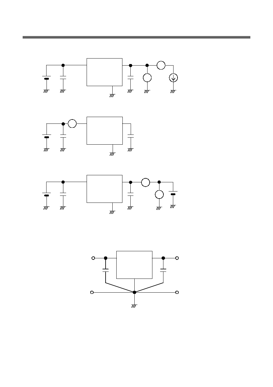
Test Circuits
1
.
VSS
VOUT
VIN
V
A
+
+
Figure 7
2.
VSS
VOUT
VIN
A
Figure 8
3.
VSS
VOUT
VIN
V
A
+
+
Figure 9
Standard Circuit
VSS
VOUT
VIN
C
IN
*1
C
L
*2
INPUT OUTPUT
GND
Single GND
*1. C
IN
is a capacitor used to stabilize input.
*2. A ceramic capacitor of 0.1
µF or more can be used for C
L
.
Figure 10
Caution The above connection diagram and constant will not guarantee successful operation.
Perform through evaluation using the actual application to set the constant.

SUPER-SMALL PACKAGE CMOS VOLTAGE REGULATOR
Rev.2.4
_00
S-817 Series
Seiko Instruments Inc.
11
Technical Terms
1. Low ESR
ESR is the abbreviation for Equivalent Series Resistance.
Low ESR output capacitors (C
L
) can be used in the S-817 Series.
2. Output voltage (V
OUT
)
The accuracy of the output voltage is
±2.0% guaranteed under the specified conditions for input voltage,
which differs depending upon the product items, output current, and temperature.
Caution If the above conditions change, the output voltage value may vary and go out of the
accuracy range of the output voltage. See the electrical characteristics and
characteristics data for details.
3. Line regulations 1 and 2 (
V
OUT1
, V
OUT2
)
Indicate the input voltage dependencies of output voltage. That is, the values show how much the output
voltage changes due to a change in the input voltage with the output current remained unchanged.
4. Load regulation (
V
OUT3
)
Indicates the output current dependencies of output voltage. That is, the values show how much the
output voltage changes due to a change in the output current with the input voltage remained unchanged.
5. Dropout voltage (V
drop
)
Indicates a difference between input voltage (V
IN1
) and output voltage when output voltage falls by 98% of
V
OUT(E)
by gradually decreasing the input voltage (V
IN
).
V
drop
= V
IN1
-[V
OUT(E)
◊ 0.98]
SUPER-SMALL PACKAGE CMOS VOLTAGE REGULATOR
S-817 Series
Rev.2.4
_00
12
Seiko Instruments Inc.
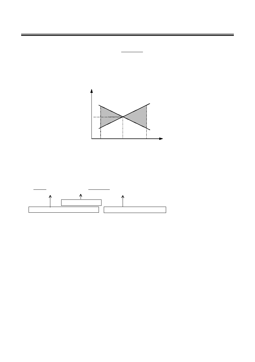
6. Temperature coefficient of output voltage
∑
OUT
OUT
V
Ta
V
The output voltage lies in the shaded area in the whole operating temperature shown in Figure 11 when
the temperature coefficient of the output voltage is
±100 ppm/∞C.
Ex. S-817A15A Typ.
-40
25
+0.15mV/∞C
V
OUT
[V]
V
OUT(E)
*1
85
Ta [
∞C]
-0.15mV/∞C
*1. V
OUT(E)
is the value of the output voltage measured at 25
∞C.
Figure 11
Temperature change ratio for output voltage [mV/∞C] is calculated by using the following equation.
[
]
[ ]
[
]
1000
C
ppm/
V
Ta
V
V
V
C
mV/
Ta
V
OUT
OUT
OUT(S)
OUT
˜
∞
∑
◊
=
∞
Specified output voltage
Output voltage temperature coefficient
Temperatures change ratio for output voltage
SUPER-SMALL PACKAGE CMOS VOLTAGE REGULATOR
Rev.2.4
_00
S-817 Series
Seiko Instruments Inc.
13
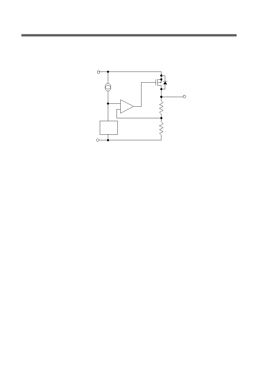
Operation
1. Basic Operation
Reference
voltage
circuit
VOUT
*1
VSS
VIN
R
S
R
f
Error amplifier
Current sauce
V
ref
-
+
*1. Parasitic diode
Figure 12
Figure 12 shows the block diagram of the S-817 series. he error amplifier compares a reference voltage
V
ref
with a part of the output voltage divided by the feedback resistors R
s
and R
f
, and supplies the gate
voltage to the output transistor, necessary to ensure certain output voltage independent from change of
input voltage and temperature.
2. Output Transistor
The S-817 series uses a P-channel MOS FET as the output transistor.
Be sure that V
OUT
does not exceed V
IN
+0.3 V to prevent the voltage regulator from being damaged due to
inverse current flowing from VOUT pin through a parastic diode to VIN pin.
3. Short Circuit Protection
The S-817A series incorporates a short circuit protection to protect the output transistor against short
circuit between VOUT pin and VSS pin. Installation of the short-circuit protection which protects the
output transistor against short-circuit between VOUT and VSS can be selected in the S-812C series. The
short-circuit protection controls output current as shown in the typical characteristics, (1) Output Voltage
versus Output Current, and suppresses output current at about 40 mA even if VOUT and VSS pins are
short-circuited.
The short-circuit protection can not be a thermal protection at the same time. Attention should be paid to
the Input voltage and the load current under the actual condition so as not to exceed the power
dissipation of the package including the case for short-circuit.
When the output current is large and the difference between input and output voltage is large even if not
shorted, the short-circuit protection may work and the output current is suppressed to the specified value.
Products without short-circuit protection can provide comparatively large current by removing a short-
circuit protection.
SUPER-SMALL PACKAGE CMOS VOLTAGE REGULATOR
S-817 Series
Rev.2.4
_00
14
Seiko Instruments Inc.
Selection of Output Capacitor (C
L
)
To stabilize operation against variation in output load, a capacitor (C
L
) must be mounted between VOUT and
VSS in the S-817 series because the phase is compensated with the help of the internal phase
compensation circuit and the ESR of the output capacitor.
When selecting a ceramic or an OS capacitor, capacitance should be 0.1
µF or more, and when selecting a
tantalum or an aluminum electrolytic capacitor, capacitance should be 0.1
µF or more and ESR 30 or less.
When an aluminum electrolytic capacitor is used attention should be especially paid to since the ESR of the
aluminum electrolytic capacitor increases at low temperature and possibility of oscillation becomes large.
Sufficient evaluation including temperature characteristics is indispensable.
Overshoot and undershoot characteristics differ depending upon the type of the output capacitor.
Refer to C
L
dependencies in "Transient Response Characteristics".
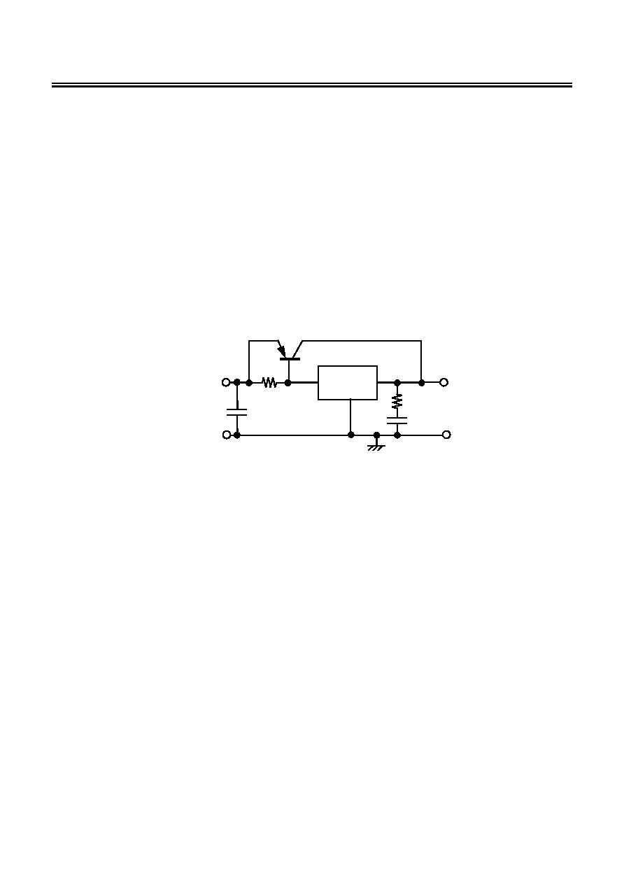
Applied Circuits
1. Output Current Boosting Circuit
R
2
R
1
Tr1
GND
VOUT
VIN
VSS
V
IN
V
OUT
C
L
S-817
series
C
IN
Figure 13
As shown in Figure 13, the output current can be boosted by externally attaching a PNP transistor. The
base current of the PNP transistor is controlled so that output voltage V
OUT
goes the voltage specified in
the S-817 when base-emitter voltage V
BE
necessary to turn on the PNP transistor is obtained between
input voltage V
IN
and S-817 power source pin VIN.
The following are tips and hints for selecting and ensuring optimum use of external parts
∑
PNP transistor Tr1:
1. Set h
FE
to approx. 100 to 400.
2. Confirm that no problem occurs due to power dissipation under normal operation conditions.
∑
Resistor R
1
:
Generally set R
1
to 1 k
˜ V
OUT (S)
(the voltage specified in the S-817 Series) or more.
Output capacitor C
L
:
Output capacitor C
L
is effective in minimizing output fluctuation at powering on or due to power or
load fluctuation, but oscillation might occur. Always connect resistor R2 in series to output capacitor
C
L
.
∑
Resistor R
2
: Set R
2
to 2
◊ V
OUT(S)
or more.
∑
DO NOT attach a capacitor between the S-817 power source VIN and GND pins or between base
and emitter of the PNP transistor to avoid oscillation.
∑
To improve transient response characteristics of the output current boosting circuit shown in Figure
13, check that no problem occurs due to output fluctuation at powering on or due to power or load
fluctuation under normal operating conditions.
∑
Pay attention to the short current limit circuit incorporated into the S-817 Series because it does not
function as a shortcircuiting protection circuit for this boosting circuit.
SUPER-SMALL PACKAGE CMOS VOLTAGE REGULATOR
Rev.2.4
_00
S-817 Series
Seiko Instruments Inc.
15
The following graphs show the examples of input-output voltage characteristics (Ta
=25∞C, typ.) in the output
current boosting circuit:
(1) S-817A11ANB/S-817B11AMC
(2) S-817A50ANB/S-817B50AMC
Tr1 : 2SA1213Y, R
1
: 1 k
, C
L
: 10
µF,
R
2
: 2
Tr1 : 2SA1213Y, R
1
:
200
, C
L
:
10
µF,
R
2
:
10
0.60
0.70
0.80
0.90
1.00
1.10
1.20
1.4 1.5 1.6 1.7 1.8 1.9 2
2.1 2.2 2.3 2.4
V
IN
(V)
V
OU
T
(V)
800 mA
600 mA
400 mA
200 mA
10 mA
50 mA
100 mA
1 mA
4.60
4.70
4.80
4.90
5.00
5.10
5.20
5.2
5.3
5.4
5.5
5.6
5.7
5.8
5.9
V
IN
(V)
V
OU
T
(V
)
100 mA
50 mA
10 mA
5 mA
800 mA
600 mA
400 mA
200 mA
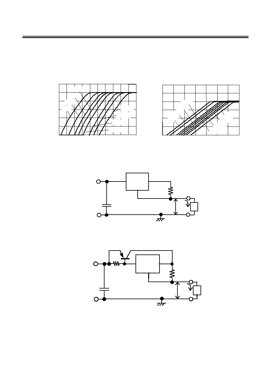
2. Constant Current Circuit
(1) Constant Current Circuit
GND
R
L
VOUT
VIN
V
IN
V0
V
O
I
O
C
IN
VSS
S-817
Series
Figure 14
(2) Constant Current Boosting Circuit
I
O
R
1
GND
R
L
VOUT
V
IN
V0
C
IN
VSS
S-817
Series
Tr1
V
O
Figure 15
SUPER-SMALL PACKAGE CMOS VOLTAGE REGULATOR
S-817 Series
Rev.2.4
_00
16
Seiko Instruments Inc.
The S-817 Series can be configured as a constant current circuit. See Figure 14 & 15.
Constant amperage I
O
is calculated using the following equation (V
OUT(E)
: Effective output voltage):
I
O
= (V
OUT(E)
˜ R
L
)
+I
SS
.
Please note that it is impossible to set constant amperage I
O
in case of circuit (1) of Figure 14 to the
value exceeding the drive ability of the S-817.
However, circuit (2) of Figure 15 is an example to set constant amperage to the value exceeding the
drive ability of the S-817. Circuit (2) incorporates a current boosting circuit. The maximum input voltage
of the constant current circuit is the value obtained by adding 10 V to voltage V
O
of the device. It is not
recommended to attach a capacitor between the S-817 power source VIN and VSS pins or between
output VOUT and VSS pins because rush current flows at powering on. An example of input voltage
between V
IN
and V
O
in circuit (2) vs. I
O
current characteristics
V
IN,
V
O
pins,
Input
voltage - I
O
current
S-817A11ANB, S-817B11AMC, Tr : 2SK1213Y, R
1 :
1 k
, V
O
=2 V
0.00
0.10
0.20
0.30
0.40
0.50
0.60
1.4 1.6 1.8 2 2.2 2.4
V
IN
-V
O
(V)
I
O
(A
)
R
L
=1.83
2.2
2.75
3.67
5.5
11
SUPER-SMALL PACKAGE CMOS VOLTAGE REGULATOR
Rev.2.4
_00
S-817 Series
Seiko Instruments Inc.
17
3. Output Voltage Adjustment Circuit
GND
V0
R
2
R
1
VOUT
VIN
V
IN
C
L
C1
C
IN
VSS
S-817
Series
Figure 16
The output voltage can be boosted by using the configuration shown in Figure 16. The output Voltage V
O
can be calculated using the following equation (V
OUT(E)
:Effective output voltage):
V
O
= V
OUT(E)
◊ (R
1
+ R
2
)
˜ R
1
+ R
2
◊ I
SS
Set R
1
and R
2
to high values of resistance so as not to be affected by current consumption I
SS.
Capacitor C1 is effective in minimizing output fluctuation at powering on or due to power or load fluctuation.
Determine the optimum value on your actual device. But it is not also recommended to attach a capacitor
between the S-817 power source VIN and VSS pins or between output VOUT and VSS pins because
output fluctuation or oscillation at powering on might occur. As shown in figure 16, a capacitor must be
mounted between VIN and GND, and between VOUT and GND.
Precautions
∑ Design wiring patterns for VIN, VOUT and GND pins to hold low impedance.
When mounting an output capacitor between the VOUT and VSS pins (C
L
) and a capacitor for
stabilizing the input between VIN and VSS pins (C
IN
), the distance from the capacitor to the VOUT pin
and to the VSS pin should be as short as possible.
∑ Note that output voltage may be increased at low load current of less than 1 µA.
∑ To prevent oscillation, it is recommended to use the external parts under the following conditions.
Output capacitor (C
L
): 0.1
µF or more
Equivalent Series Resistance (ESR): 30
or less
Input series resistance (R
IN
): 10
or less
∑ A voltage regulator may oscillate when power source impedance is high and input capacitor is low or
not connected.
∑ The application condition for input voltage and load current should not exceed the package power
dissipation.
∑ SII claims no responsibility for any and all disputes arising out of or in connection with any infringement
of the products including this IC upon patents owned by a third party.
∑ Do not apply an electrostatic discharge to this IC that exceeds the performance ratings of the built-in
electrostatic protection circuit.
SUPER-SMALL PACKAGE CMOS VOLTAGE REGULATOR
S-817 Series
Rev.2.4
_00
18
Seiko Instruments Inc.
Typical Operating Characteristics
(1) Output Voltage vs. Output Current (when load current increases)
(a) S-817A Series
S-817A11A(Ta=25∞C)
0.0
0.3
0.6
0.9
1.2
0
20
40
60
80
I
OUT
(mA)
V
OUT
(V)
V
IN
=
1.5V
2.1V
3.1V
4.1V
8V
S-817A20A(Ta=25∞C)
0.0
0.5
1.0
1.5
2.0
2.5
0
30
60
90
120
I
OUT
(mA)
V
IN
=
2.4V
3V
10V
5V
4V
V
OUT
(V)
S-817A30A(Ta=25 ∞ C)
0.0
0.5
1.0
1.5
2.0
2.5
3.0
0 30 60 90 120
150
I
OUT
(mA)
4V
V
IN
=
3.4V
5V
6V
10V
V
OUT
(V)
S-817A50A(Ta=25 ∞ C)
0.0
1.0
2.0
3.0
4.0
5.0
0 40 80 120
160
200
I
OUT
(mA)
V
IN
=5.4V
6V
7V
8V
10V
V
OUT
(V)
(b) S-817B series
S-817B11A(Ta=25∞C)
0.0
0.3
0.6
0.9
1.2
0 50 100
150
200
250
I
OUT
(mA)
V
OUT
(V)
V
IN
=
1.5V
2.1V
3.1V
4.1V
8V
S-817B20A(Ta=25∞C)
0.0
0.5
1.0
1.5
2.0
2.5
0 50 100
150
200
250
300
I
OUT
(mA)
V
OUT
(V)
V
IN
=2.4V
3V
4V
5V
10V
S-817B30A(Ta=25∞C)
0.0
0.5
1.0
1.5
2.0
2.5
3.0
3.5
0 50 100
150
200
250
300
I
OUT
(mA)
V
OUT
(V)
V
IN
=
3.4V
4V
5V
6V
10V
S-817B50A(Ta=25∞C)
0.0
1.0
2.0
3.0
4.0
5.0
0 50 100
150
200
250
300
I
OUT(
mA)
V
OUT
(V)
V
IN
=5.4V
6V
7V
8V
10V
SUPER-SMALL PACKAGE CMOS VOLTAGE REGULATOR
Rev.2.4
_00
S-817 Series
Seiko Instruments Inc.
19
(2) Output Voltage vs. Input Voltage
S-817A11A/S-817B11A(Ta=25∞C)
0.0
0.5
1.0
1.5
0 2 4 6 8 10
V
IN
(V)
I
OUT
1mA
10mA
20mA
=1
µ A
V
OUT
(V)
S-817A20A/S-817B20A(Ta=25∞C)
0.0
0.5
1.0
1.5
2.0
2.5
0
2
4
6
8
10
V
IN
(V)
I
OUT
=1
µA
1mA
10mA
20mA
50mA
V
OUT
(V)
S-817A30A/S-817B30A(Ta=25∞C)
0.0
0.5
1.0
1.5
2.0
2.5
3.0
3.5
0
2
4
6
8
10
V
IN
(V)
I
OUT
=1
µA
1mA
20mA
50mA
10mA
V
OUT
(V)
S-817A50A/S-817B50A(Ta=25∞C)
0.0
1.0
2.0
3.0
4.0
5.0
0
2
4
6
8
10
V
IN
(V)
I
OUT
=1
µA
1mA
10mA
20mA
50mA
V
OUT
(V)
SUPER-SMALL PACKAGE CMOS VOLTAGE REGULATOR
S-817 Series
Rev.2.4
_00
20
Seiko Instruments Inc.
(3) Maximum Output Current vs. Input Voltage
(a) S-817A Series
S-817A11A
0
20
40
60
80
100
0 2 4 6 8 10
V
IN
(V)
I
OUT
max.(mA)
Ta=-40 ∞ C
25 ∞ C
85 ∞ C
S-817A20A
0
20
40
60
80
100
120
1
3
5
7
9
V
IN
(V)
Ta=-40∞C
25∞C
85∞C
I
OUT
max.(mA)
S-817A30A
0
30
60
90
120
150
180
2
4
6
8
10
V
IN
(V)
Ta=-40∞C
25∞C
85∞C
I
OUT
max.(mA)
S-817A50A
0
50
100
150
200
250
4
6
8
10
V
IN
(V)
Ta=-40∞C
25∞C
85∞C
I
OUT
max.(mA)
(b) S-817B Series
S-817B11A
0
50
100
150
200
250
300
0 2 4 6 8 10
V
IN
(V)
I
OUT
max.(mA)
Ta=-40∞C
25∞C
85∞C
S-817B20A
0
50
100
150
200
250
300
0 2 4 6 8 10
V
IN
(V)
I
OUT
max.(mA)
Ta=-40∞C
25∞C
85∞C
S-817B30A
0
50
100
150
200
250
300
2 4 6 8 10
V
IN
(V)
I
OUT
max.(mA)
Ta=-40∞C
25∞C
85∞C
S-817B50A
0
50
100
150
200
250
300
4 6 8 10
V
IN
(V)
I
OUT
max.(mA)
Ta=-40∞C
25∞C
85∞C

SUPER-SMALL PACKAGE CMOS VOLTAGE REGULATOR
Rev.2.4
_00
S-817 Series
Seiko Instruments Inc.
21
(4) Dropout Voltage vs. Output Current
S-817A11A/S-817B11A
0
500
1000
1500
2000
0 5 10
15 20
I
OUT
(mA)
V
dr
o
p
(m
V)
Ta=-40∞C
25∞C
85∞C
S-817A20A/S-817B20A
0
500
1000
1500
2000
0 10 20 30 40
I
OUT
(mA)
V
dr
o
p
(m
V)
Ta=-40∞C
25∞C
85∞C
S-817A30A/S-817B30A
0
400
800
1200
1600
0 10 20 30 40 50
I
OUT
(mA)
V
dr
o
p
(m
V)
Ta=-40∞C
25∞C
85∞C
S-817A50A/S-817B50A
0
200
400
600
800
1000
0 10 20 30 40 50
I
OUT
(mA)
V
dr
o
p
(m
V)
Ta=-40∞C
25∞C
85∞C
(5) Output Voltage vs. Ambient Temperature
S-817A11A/S-817B11A
1.08
1.09
1.10
1.11
1.12
-50
0
50
100
Ta(∞C)
(V
)
V
OU
T
V
IN
=3.1V,I
OUT
=10mA
S-817A20A/S-817B20A
1.96
1.98
2.00
2.02
2.04
-50
0
50
100
Ta(∞C)
(V
)
V
IN
=4V,I
OUT
=10mA
V
OU
T
S-817A30A/S-817B30A
2.94
2.97
3.00
3.03
3.06
-50
0
50
100
Ta(∞C)
(V
)
V
IN
=5V,I
OUT
=10mA
V
OU
T
S-817A50A/S-817B50A
4.90
4.95
5.00
5.05
5.10
-50
0
50
100
Ta(∞C)
(V
)
V
IN
=7V,I
OUT
=10mA
V
OU
T
SUPER-SMALL PACKAGE CMOS VOLTAGE REGULATOR
S-817 Series
Rev.2.4
_00
22
Seiko Instruments Inc.
(6) Line Regulation 1 vs. Ambient Temperature
(7) Line Regulation 2 vs. Ambient Temperature
S-817B11/20/30/50A
S-817A11/20/30/50A
0
5
10
15
20
25
30
-50 -25 0 25 50 75 100
Ta(∞C)
V
OU
T
1
(m
V)
3V
2V
V
OUT
=1.1V
5V
V
IN
=V
OUT(S)
+1V10V,I
OUT
=1mA
S-817B11/20/30/50A
S-817A11/20/30/50A
0
5
10
15
20
25
30
-50 -25 0 25 50 75 100
Ta(∞C)
V
OU
T
2
(
mV
)
3V
2V
V
OUT
=1.1V
5V
V
IN
=V
OUT(S)
+1V10V,I
OUT
=1
µA
(8) Load Regulation vs. Ambient Temperature
S-817B11/20/30/50A
S-817A11/20/30/50A
0
10
20
30
40
50
60
70
80
-50 -25 0 25 50 75 100
Ta(∞C)
V
OU
T
3
(
mV
)
2V(I
OUT
=20mA)
V
OUT
=1.1V(I
OUT
=10mA)
3V(I
OUT
=30mA)
5V(I
OUT
=50mA)
V
IN
=V
OUT(S)
+2V,I
OUT
=1
µAI
OUT

SUPER-SMALL PACKAGE CMOS VOLTAGE REGULATOR
Rev.2.4
_00
S-817 Series
Seiko Instruments Inc.
23
(9) Current Consumption vs. Input Voltage
S-817A11A/S-817B11A
0
0.4
0.8
1.2
1.6
0 2 4 6 8 10
V
IN
(V)
I
SS1
(
µ
A)
85∞C
Ta=-40∞C
25∞C
S-817A20A/S-817B20A
0
0.4
0.8
1.2
1.6
0 2 4 6 8 10
V
IN
(V)
I
SS1
(
µ
A
)
Ta=-40∞C
25∞C
85∞C
S-817A30A/S-817B30A
0
0.4
0.8
1.2
1.6
0 2 4 6 8 10
V
IN
(V)
I
SS1
(
µ
A)
Ta=-40∞C
25∞C
85∞C
S-817A50A/S-817B50A
0
0.4
0.8
1.2
1.6
0 2 4 6 8 10
V
IN
(V)
I
SS1
(u
A
)
Ta=-40∞C
25∞C
85∞C
SUPER-SMALL PACKAGE CMOS VOLTAGE REGULATOR
S-817 Series
Rev.2.4
_00
24
Seiko Instruments Inc.
REFERENCE DATA
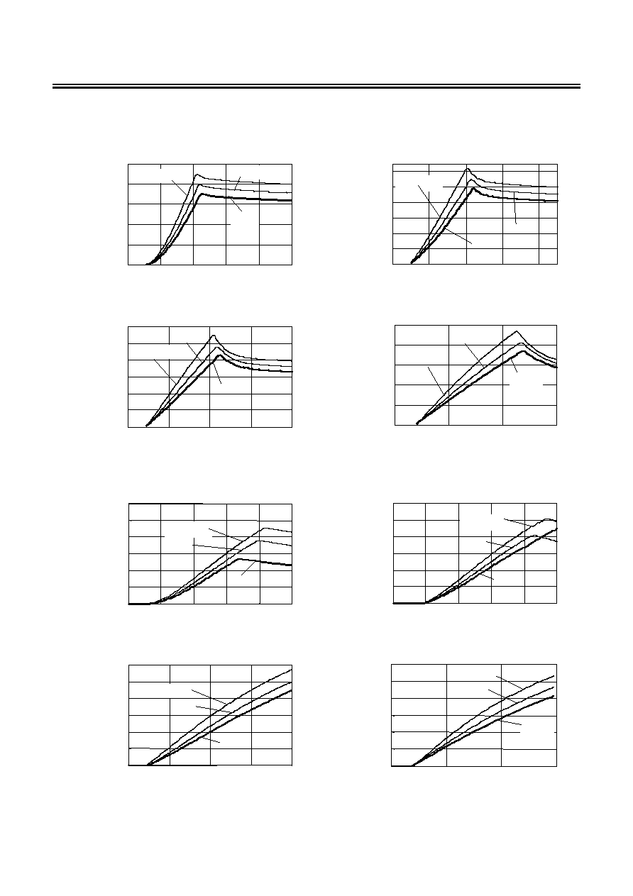
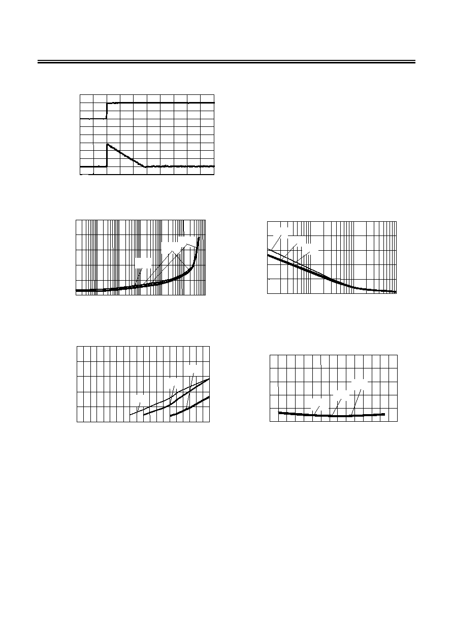
Transient Response Charcteristics (Typical data:Ta
=
=
=
=25 ∞∞∞∞C)
O v e rs h o o t
In p u t v o lta g e
O u tp u t v o lta g e
o r
L o a d c u rre n t
U n d e rs h o o t
(1) At powering on S-817A30A (when using a ceramic capacitor, C
L
=
=
=
=1 µµµµF)
TIME(100
µs/div)
V
OUT
(0.5 V/div)
10 V
0 V
3 V
V
IN
=0 V10 V, I
OUT
=10 mA, C
L
=1 µF
Load dependencies of overshoot at powering on
C
L
dependencies of overshoot at powering on
0
0.01
0.02
0.03
0.04
0.05
1.E-07
1.E-06
1.E-05
1.E-04
1.E-03
1.E-02
1.E-01
I
OUT
(A)
Ov
er
S
hoot(
V
)
2V
3V
5V
V
OUT
=0 V
V
OUT(S)
+2 V, C
L
=1
µF
0
0.01
0.02
0.03
0.04
0.05
0.01
0.1
1
10
C
L
(
µF)
O
v
er Shoot(V)
2V
3V
5V
V
IN
=0 VV
OUT(S)
+2 V, I
OUT
=10 mA
V
DD
dependencies of overshoot at powering on
"Ta" dependencies of overshoot at powering on
0
0.01
0.02
0.03
0.04
0.05
0
2
4
6
8
10
V
DD
(V)
Ov
er
S
hoot(
V
)
2V
3V
5V
V
IN
=0 VV
DD,
I
OUT
=10 mA, C
L
=1 µF
0
0.01
0.02
0.03
0.04
0.05
-50
0
50
100
Ta(∞C)
O
v
er Shoot(V)
2V
3V
5V
V
IN
=0 VV
OUT(S)
+2 V, I
OUT
=10 mA, C
L
=1 µF
SUPER-SMALL PACKAGE CMOS VOLTAGE REGULATOR
Rev.2.4
_00
S-817 Series
Seiko Instruments Inc.
25
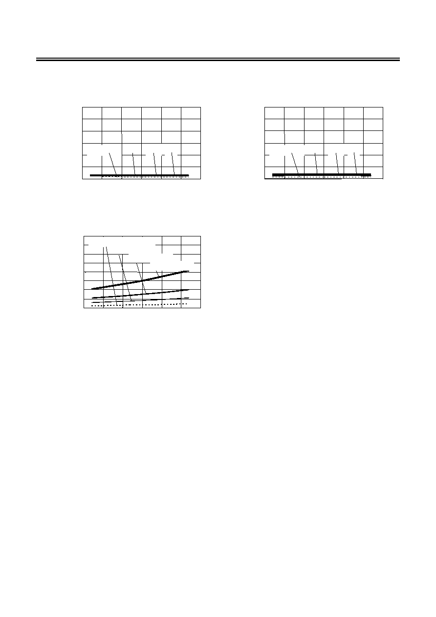
(2) At powering on S-817B30A (when using a ceramic capacitor, C
L
=
=
=
=1 µµµµF)
V
IN
=0 V10 V, I
OUT
=10 mA, C
L
=1 µF
TIME(100
µs/div)
V
OUT
(0.5 V/div)
10 V
0 V
3 V
Load dependencies of overshoot at powering on
C
L
dependencies of overshoot at powering on
0
0.01
0.02
0.03
0.04
0.05
1.E-07
1.E-06
1.E-05
1.E-04
1.E-03
1.E-02
1.E-01
I
OUT
(A)
Ov
er
S
hoot(
V
)
2V
3V
5V
V
IN
=0 VV
OUT(S)
+2 V, C
L
=1 µF
0
0.01
0.02
0.03
0.04
0.05
0.01
0.1
1
10
C
L
(
µF)
O
v
er Shoot(V)
2V
3V
5V
V
IN
=0 VV
OUT(S)
+2 V, I
OUT
=10 mA
V
DD
dependencies of overshoot at powering on
"Ta" dependencies of overshoot at powering on
0
0.01
0.02
0.03
0.04
0.05
0
2
4
6
8
10
V
DD
(V)
Ov
er
S
hoot(
V
)
2V
3V
5V
V
IN
=0 VV
DD,
I
OUT
=10 mA, C
L
=1 µF
0
0.01
0.02
0.03
0.04
0.05
-50
0
50
100
Ta(∞C)
O
v
er Shoot(V)
2V
3V
5V
V
IN
=0 VV
OUT(S)
+2 V, I
OUT
=10 mA, C
L
=1 µF
SUPER-SMALL PACKAGE CMOS VOLTAGE REGULATOR
S-817 Series
Rev.2.4
_00
26
Seiko Instruments Inc.
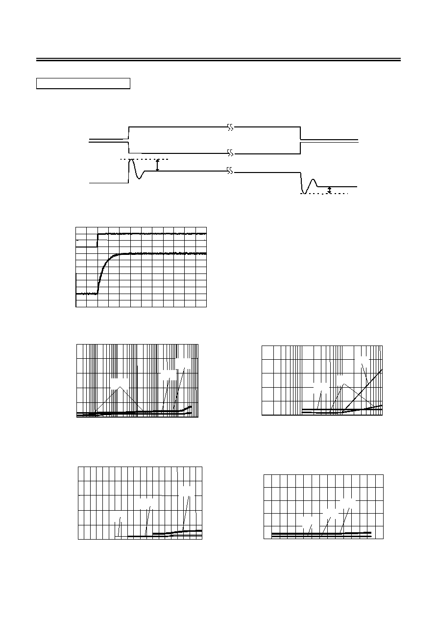
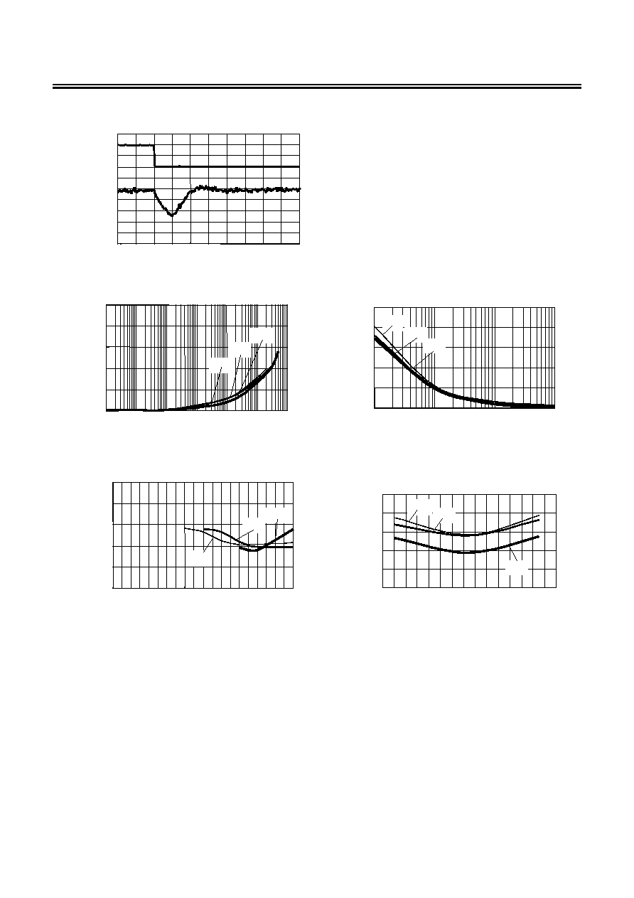
(3) Power fluctuation S-817A30A (when using a ceramic capacitor, C
L
=
=
=
=1 µµµµF)
V
IN
=4 V10 V,I
OUT
=1 mA, C
L
=1 µF
TIME(200
µ s/div)
V
OUT
(0.2 V/div)
10 V
4 V
3 V
Load dependencies of overshoot at power fluctuation C
L
dependencies of overshoot at power fluctuation
0
0.1
0.2
0.3
0.4
0.5
1.E-07 1.E-06 1.E-05 1.E-04 1.E-03 1.E-02 1.E-01
I
OUT
(A)
O
v
e
r
Shoot
(
V
)
2 V
3 V
5 V
V
IN
=V
OUT(S)
+1 V V
OUT(S)
+2 V, C
L
=1 µF
0
0.2
0.4
0.6
0.8
1
0.01 0.1 1 10
C
L
(
µF)
O
v
e
r
Sh
o
o
t(
V)
2 V
3 V
5 V
V
IN
=V
OUT(S)
+1 VV
OUT(S)
+2 V, I
OUT
=1 mA
V
DD
dependencies of overshoot at power fluctuation "Ta" dependencies of overshoot at power fluctuation
0
0.2
0.4
0.6
0.8
1
0
2
4
6
8
10
V
DD
(V)
O
v
er Shoot(V)
2V
3V
5V
V
IN
=V
OUT(S)
+1 VV
DD
, I
OUT
=1 mA, C
L
=1 µF
0
0.2
0.4
0.6
0.8
1
-50
0
50
100
Ta(∞C)
O
v
er Shoot(V)
2V
3V
5V
V
IN
=V
OUT(S)
+1 VV
OUT(S)
+2 V, I
OUT
=1 mA, C
L
=1 µF
SUPER-SMALL PACKAGE CMOS VOLTAGE REGULATOR
Rev.2.4
_00
S-817 Series
Seiko Instruments Inc.
27
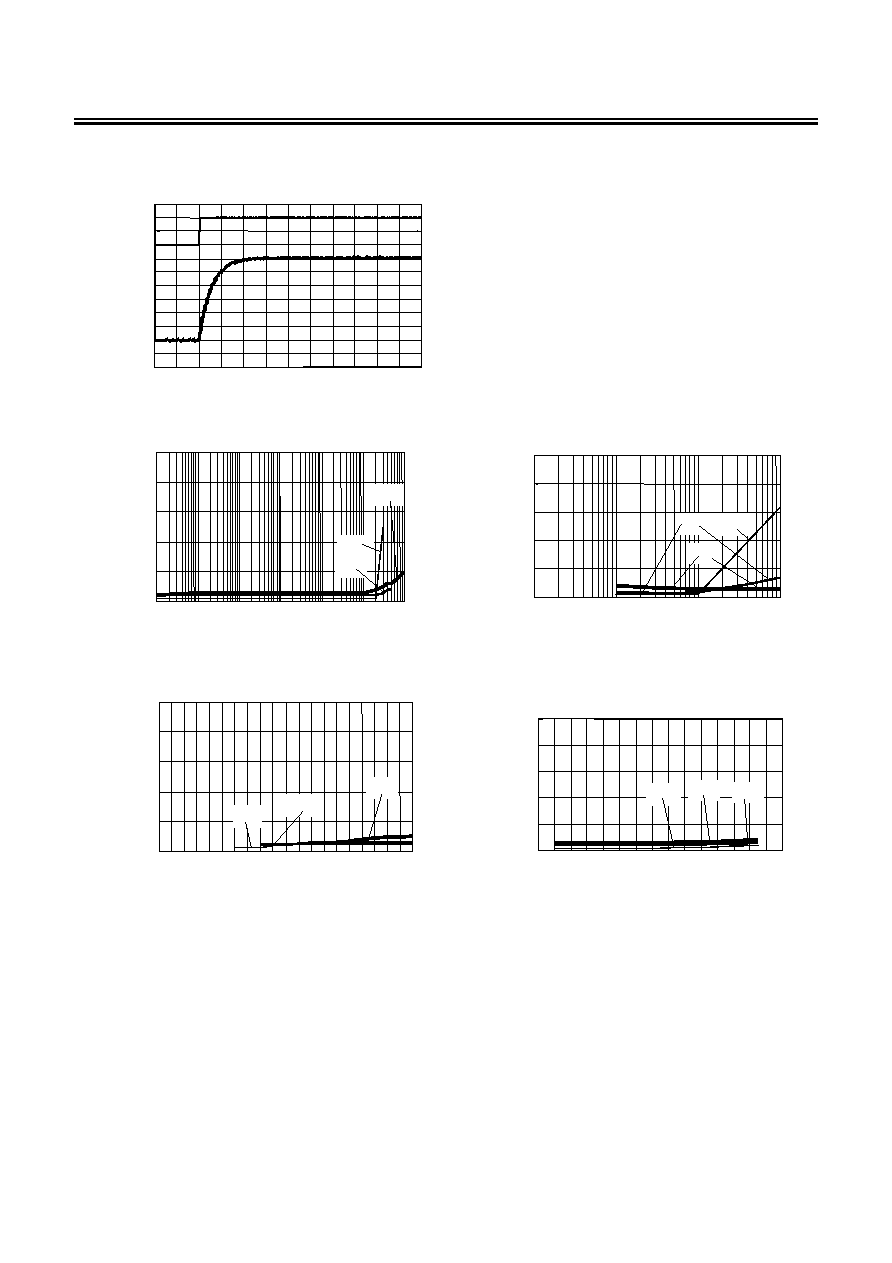
V
IN
=10 V4 V,I
OUT
=1 mA, C
L
=1 µF
TIME(50
µs/div)
V
OUT
(0.02 V/div)
10 V
3 V
4 V
Load dependencies of undershoot at power fluctuation C
L
dependencies of undershoot at power fluctuation
0
0.1
0.2
0.3
0.4
0.5
1.E-07
1.E-06
1.E-05
1.E-04
1.E-03
1.E-02
1.E-01
I
OUT
(A)
U
nder Sho
o
t(V)
2V
3V
5V
V
IN
=V
OUT(S)
+2 VV
OUT(S)
1 V, C
L
=1 µF
0
0.2
0.4
0.6
0.8
1
0.01
0.1
1
10
C
L
(
µF)
U
nder Sho
o
t(V)
2V
3V
5V
V
IN
=V
OUT(S)
+2 VV
OUT(S)
+1 V, I
OUT
=1 mA
V
DD
dependencies of undershoot at power fluctuation "Ta" dependencies of undershoot at power fluctuation
0
0.02
0.04
0.06
0.08
0.1
0
2
4
6
8
10
V
DD
(V)
U
nder Sho
o
t(V)
2V
3V
5V
V
IN
=V
DD
V
OUT(S)
+1 V, I
OUT
=1 mA, C
L
=1 µF
0
0.02
0.04
0.06
0.08
0.1
-50
0
50
100
Ta(∞C)
U
nder Sho
o
t(V)
2V
3V
5V
V
IN
=V
OUT(S)
+2 VV
OUT(S)
+1 V, I
OUT
=1 mA, C
L
=1 µF
SUPER-SMALL PACKAGE CMOS VOLTAGE REGULATOR
S-817 Series
Rev.2.4
_00
28
Seiko Instruments Inc.
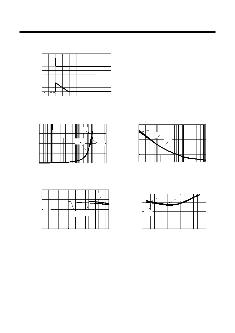
(4) Load fluctuation S-817A30A/S-817B30A (when using a ceramic capacitor, C
L
=
=
=
=1 µµµµF)
I
OUT
=30 mA10 µA,V
IN
=5 V, C
L
=1 µF
TIME(20 ms/div)
V
OUT
(0.2 V/div)
10
µA
3 V
30 mA
Load current dependencies of overshoot at load
fluctuation
C
L
dependencies of overshoot at load fluctuation
0
0.5
1
1.5
2
1.E-05
1.E-04
1.E-03
1.E-02
1.E-01
1.E+00
I
OUT
(A)
O
v
er Shoot(V)
2V
3V
5V
V
IN
=V
OUT(S)
+2 V, I
OUT
=I
L
10 µA, C
L
=1 µF
0
0.2
0.4
0.6
0.8
1
0.01
0.1
1
10
C
L
(
µF)
O
v
er Shoot(V)
2V
3V
5V
V
IN
=V
OUT(S)
+2 V, I
OUT
=10 mA10 µA
V
DD
dependencies of overshoot at load fluctuation
"Ta" dependencies of overshoot at load fluctuation
0
0.05
0.1
0.15
0.2
0
2
4
6
8
10
V
DD
(V)
O
v
er Shoot(V)
2V
3V
5V
V
IN
=V
DD
, I
OUT
=10 mA,10 µA, C
L
=1 µF
0
0.05
0.1
0.15
0.2
-50
0
50
100
Ta(∞C)
O
v
er Shoot(V)
2V
3V
5V
V
IN
=V
OUT(S)
+2 V, I
OUT
=10 mA10 µA, C
L
=1 µF
SUPER-SMALL PACKAGE CMOS VOLTAGE REGULATOR
Rev.2.4
_00
S-817 Series
Seiko Instruments Inc.
29
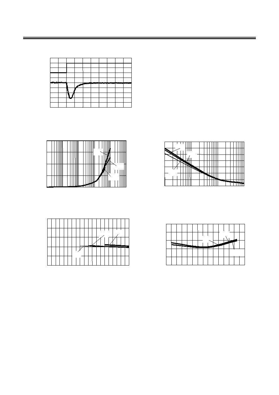
I
OUT
=10
µA30mA, V
IN
=5V, C
L
=1
µF
TIME(50 ms/div)
V
OUT
(0.2V/div)
30mA
3V
10
µA
Load current dependencies of undershoot at load
fluctuation
C
L
dependencies of undershoot at load fluctuation
0
0.5
1
1.5
2
1.E-05
1.E-04
1.E-03
1.E-02
1.E-01
1.E+00
I
OUT
(A)
U
nder Sho
o
t(V)
2V
3V
5V
V
IN
=V
OUT(S)
+2 V, I
OUT
=10 µAI
L,
C
L
=1 µA
0
0.2
0.4
0.6
0.8
1
1.2
1.4
0.01
0.1
1
10
C
L
(
µF)
U
nder Sho
o
t(V)
2V
3V
5V
V
IN
=V
OUT(S)
+2 V, I
OUT
=10 µA10 mA
V
DD
dependencies of undershoot at load fluctuation
"Ta" dependencies of undershoot at load fluctuation
0
0.1
0.2
0.3
0.4
0.5
0
2
4
6
8
10
V
DD
(V)
U
nder Sho
o
t(V)
2V
3V
5V
V
IN
=V
DD
, I
OUT
=10 µA10 mA, C
L
=1 µF
0
0.1
0.2
0.3
0.4
0.5
-50
0
50
100
Ta(∞C)
U
nder Sho
o
t(V)
2V
3V
5V
V
IN
=V
OUT(S)
+2 V, I
OUT
=10 µA 10 mA, C
L
=1 µF

No.
TITLE
SCALE
UNIT
mm
Seiko Instruments Inc.
0.3
+0.1
-0.05
0.4
+0.1
-0.05
0.05
1
2
4
3
0.16
+0.1
-0.06
1.3±0.2
2.0±0.2
No. NP004-A-P-SD-1.1
SC82AB-A-PKG Dimensions
NP004-A-P-SD-1.1
No.
TITLE
SCALE
UNIT
mm
Seiko Instruments Inc.
1.1±0.1
0.2±0.05
4.0±0.1
2.0±0.05
4.0±0.1
1.5
1.05±0.1
+0.1
-0.05
2.2±0.2
(0.7)
No. NP004-A-C-SD-2.1
NP004-A-C-SD-2.1
SC82AB-A-Carrier Tape
Feed direction
No.
TITLE
SCALE
UNIT
mm
Seiko Instruments Inc.
QTY.
3,000
(60∞)
(60∞)
¯13±0.2
12.5max.
9.0±0.3
No. NP004-A-R-SD-1.1
NP004-A-R-SD-1.1
SC82AB-A-Reel
Enlarged drawing in the central part

No.
TITLE
SCALE
UNIT
mm
Seiko Instruments Inc.
2.9±0.2
1.9±0.2
0.95±0.1
0.4±0.1
0.16
+0.1
-0.06
1
2
3
4
5
No. MP005-A-P-SD-1.2
MP005-A-P-SD-1.2
SOT235-A-PKG Dimensions
No.
TITLE
SCALE
UNIT
mm
Seiko Instruments Inc.
¯1.5
+0.1
-0
2.0±0.05
¯1.0
+0.2
-0
4.0±0.1
1.4±0.2
0.25±0.1
3.2±0.2
1
2
3
4
5
No. MP005-A-C-SD-2.1
MP005-A-C-SD-2.1
SOT235-A-Carrier Tape
Feed direction
4.0±0.1(10 pitches:40.0±0.2)
No.
TITLE
SCALE
UNIT
mm
Seiko Instruments Inc.
12.5max.
9.0±0.3
¯13±0.2
(60∞)
(60∞)
QTY.
3,000
No. MP005-A-R-SD-1.1
MP005-A-R-SD-1.1
SOT235-A-Reel
Enlarged drawing in the central part
No.
TITLE
SCALE
UNIT
mm
Seiko Instruments Inc.
0.4±0.05
1.5±0.1
4.5±0.1
1.6±0.2
1.5±0.1 1.5±0.1
0.45±0.1
0.4±0.1
0.4±0.1
45∞
3
1
2
No. UP003-A-P-SD-1.1
UP003-A-P-SD-1.1
SOT893-A-PKG Dimensions
No.
TITLE
SCALE
UNIT
mm
Seiko Instruments Inc.
2.0±0.1
0.3±0.05
8.0±0.1
¯1.5
+0.1
-0
2.0±0.05
¯1.5
+0.1
-0
4.75±0.1
5∞ max.
No. UP003-A-C-SD-1.1
UP003-A-C-SD-1.1
SOT893-A-Carrier Tape
Feed direction
4.0±0.1(10 pitches : 40.0±0.2)
No.
TITLE
SCALE
UNIT
mm
Seiko Instruments Inc.
13.0±0.3
16.5max.
(60∞)
(60∞)
QTY.
1,000
No. UP003-A-R-SD-1.1
UP003-A-R-SD-1.1
SOT893-A-Reel
Enlarged drawing in the central part

No.
TITLE
SCALE
UNIT
mm
Seiko Instruments Inc.
5.2max.
4.2max.
0.6max.
0.45±0.1
0.45±0.1
1.27
No. YS003-B-P-SD-1.1
YS003-B-P-SD-1.1
TO92-B-PKG Dimensions
Marked side
No.
TITLE
SCALE
UNIT
mm
Seiko Instruments Inc.
4.2max.
0.45±0.1
Marked side
1.27
5.2max.
0.45±0.1
0.6max.
2.5
+0.4
-0.1
No. YF003-A-P-SD-1.1
YF003-A-P-SD-1.1
TO92-A-PKG Dimensions
No.
TITLE
SCALE
UNIT
mm
Seiko Instruments Inc.
12.7±1.0
6.35±0.4
¯4.0±0.2
0.5max.
1#pin
3#pin
1.0max.
1.0max.
0.7±0.2
1.45max.
No. YF003-A-C-SD-4.1
YF003-A-C-SD-4.1
TO92-A-Radial Tape
Marked side
12.7±0.3(20 pitches : 254.0±1.0)
Feed direction
Feed direction
Marked side
No.
TITLE
SCALE
UNIT
mm
Seiko Instruments Inc.
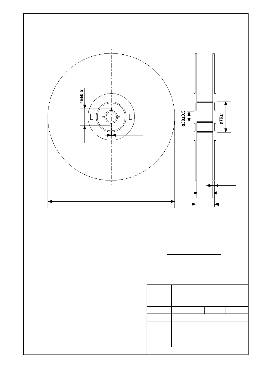
¯358±2
43±0.5
53±0.5
5±0.5
2±0.5
QTY.
2,000
No. YF003-A-R-SD-2.1
YF003-A-R-SD-2.1
TO92-A-Reel

No.
TITLE
SCALE
UNIT
mm
Seiko Instruments Inc.
4.2max.
0.45±0.1
Marked side
1.27
5.2max.
0.45±0.1
0.6max.
2.5
+0.4
-0.1
No. YF003-A-P-SD-1.1
YF003-A-P-SD-1.1
TO92-A-PKG Dimensions
No.
TITLE
SCALE
UNIT
mm
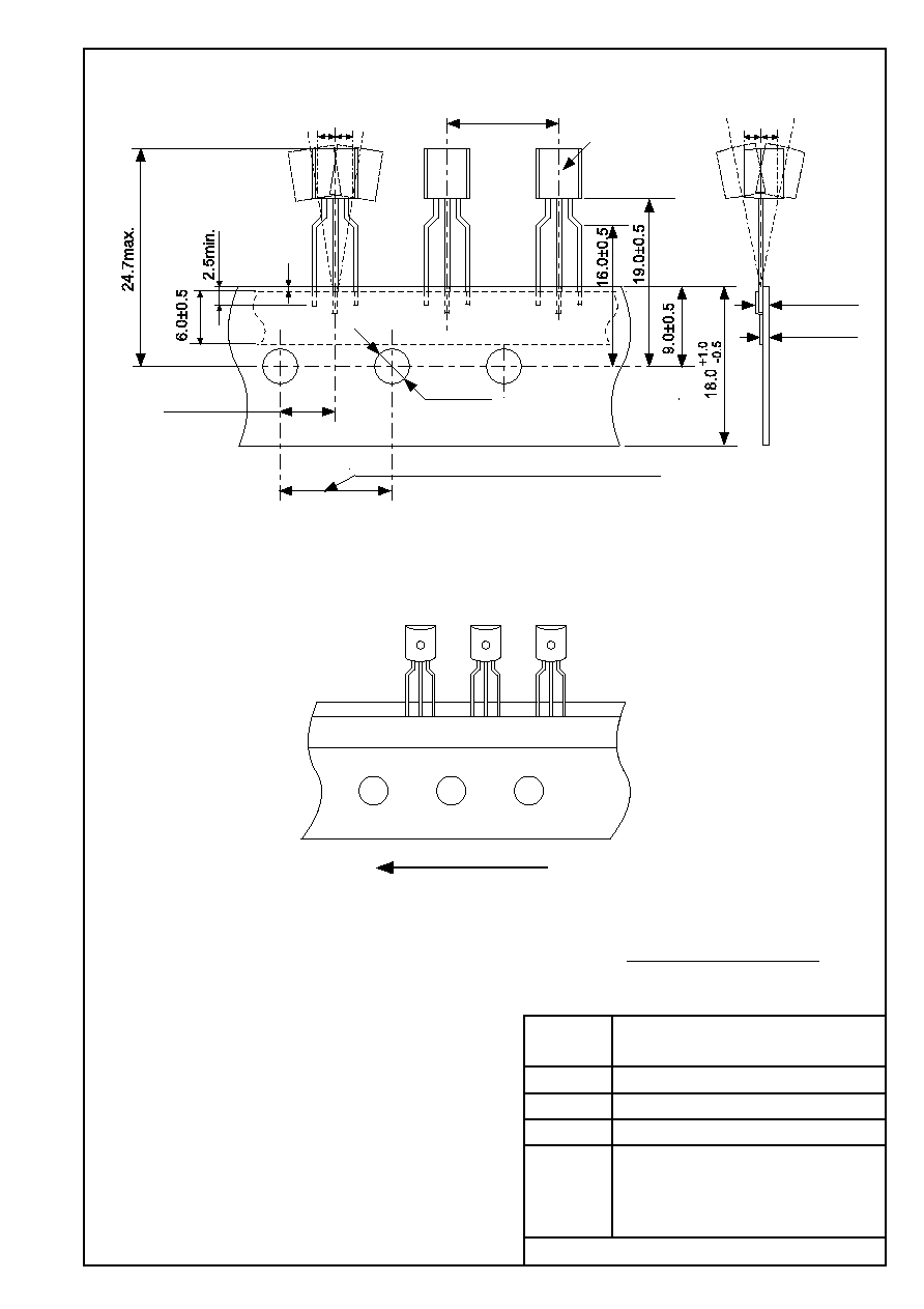
Seiko Instruments Inc.
12.7±1.0
6.35±0.4
¯4.0±0.2
0.5max.
1#pin
3#pin
1.0max.
1.0max.
0.7±0.2
1.45max.
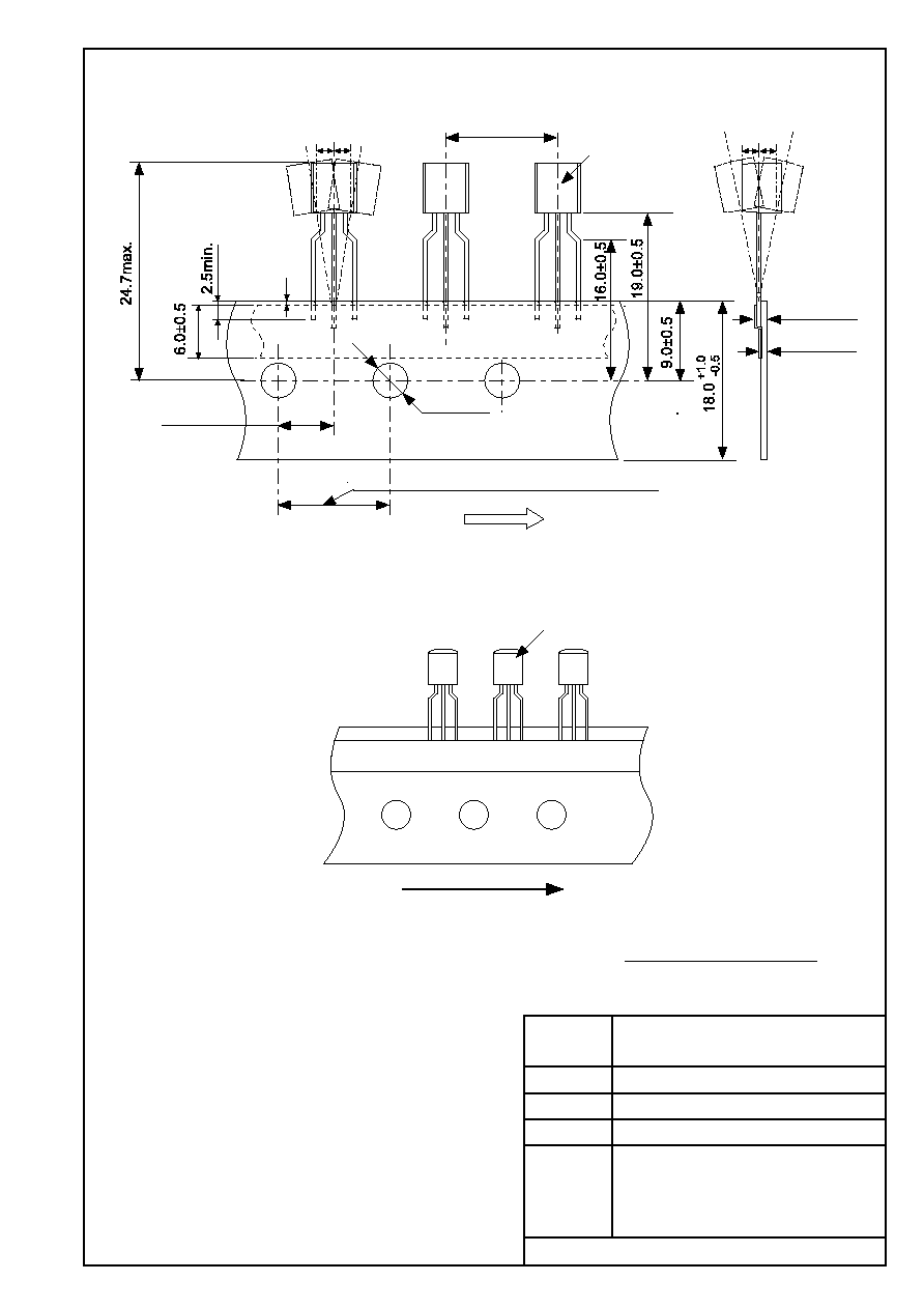
Feed direction
12.7±0.3(20 pitches : 254.0±1.0)
Marked side
No. YZ003-C-C-SD-3.1
YZ003-C-C-SD-3.1
TO92-C-Radial Tape
No.
TITLE
SCALE
UNIT
mm
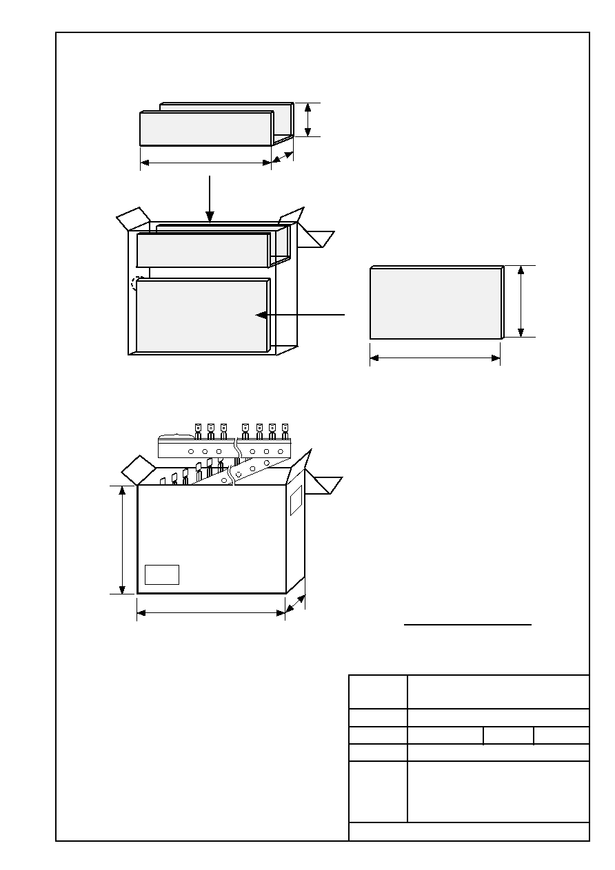
Seiko Instruments Inc.
330
47
262
Spacer
320
40
60
165
320
QTY.
2,500
No. YZ003-C-Z-SD-2.1
YZ003-C-Z-SD-2.1
Side spacer placed in front side
Space more than 4 strokes
TO92-C-Ammo Packing

∑
The information described herein is subject to change without notice.
∑
Seiko Instruments Inc. is not responsible for any problems caused by circuits or diagrams described herein
whose related industrial properties, patents, or other rights belong to third parties. The application circuit
examples explain typical applications of the products, and do not guarantee the success of any specific
mass-production design.
∑
When the products described herein are regulated products subject to the Wassenaar Arrangement or other
agreements, they may not be exported without authorization from the appropriate governmental authority.
∑
Use of the information described herein for other purposes and/or reproduction or copying without the
express permission of Seiko Instruments Inc. is strictly prohibited.
∑
The products described herein cannot be used as part of any device or equipment affecting the human
body, such as exercise equipment, medical equipment, security systems, gas equipment, or any apparatus
installed in airplanes and other vehicles, without prior written permission of Seiko Instruments Inc.
∑
Although Seiko Instruments Inc. exerts the greatest possible effort to ensure high quality and reliability, the
failure or malfunction of semiconductor products may occur. The user of these products should therefore
give thorough consideration to safety design, including redundancy, fire-prevention measures, and
malfunction prevention, to prevent any accidents, fires, or community damage that may ensue.