 | –≠–ª–µ–∫—Ç—Ä–æ–Ω–Ω—ã–π –∫–æ–º–ø–æ–Ω–µ–Ω—Ç: S-818 | –°–∫–∞—á–∞—Ç—å:  PDF PDF  ZIP ZIP |
Document Outline
- ˛ˇ
- ˛ˇ
- ˛ˇ
- ˛ˇ
- ˛ˇ
- ˛ˇ
- ˛ˇ
- ˛ˇ
- ˛ˇ
- ˛ˇ
- ˛ˇ
- ˛ˇ
- ˛ˇ
- ˛ˇ
- ˛ˇ
- ˛ˇ
- ˛ˇ
- ˛ˇ
- ˛ˇ
- ˛ˇ
- ˛ˇ

Rev.1.2
Seiko Instruments Inc.
1
LOW DROPOUT CMOS VOLTAGE REGULATOR
S-818 Series
Note : Please consider power dissipation of the package when the output current is large.
Package
O
5-pin SOT-23-5 (Package drawing code: MP005-A)
O
5-pin SOT-89-5 (Package drawing code: UP005-A)
The S-818 Series is a positive voltage regulator developed
utilizing CMOS technology featured by low dropout voltage,
high output voltage accuracy and low current consumption.
Built-in low on-resistance transistor provides low dropout
voltage and large output current. A ceramic capacitor of 2
µ
F
or more can be used as an output capacitor. A power-OFF
circuit ensures long battery life.
The SOT-23-5 miniaturized package and the SOT-89-5
package are recommended for configuring portable devices
and large output current applications, respectively.
Applications
O
Power source for
battery-powered devices
O
Power source for
personal communication devices
O
Power source for home electric/electronic
appliances
Features
O
Low current consumption
During operation: Typ. 30
µ
A, Max. 40
µ
A
During power off: Typ. 100 nA, Max. 500 nA
O
Output voltage: 0.1 V steps between 2.0 and 6.0 V
O
High accuracy output voltage:
±
2.0%
O
Peak output current;
200 mA capable (3.0 V output product, V
IN
=4 V)
Note
300 mA capable (5.0 V output product, V
IN
=6 V)
Note
O
Low dropout voltage
Typ. 170 mV (5.0 V output product, I
OUT
= 60 mA)
A ceramic capacitor (2
µ
F or more) can be used as an
output capacitor.
O
Built-in power-off circuit
O
Compact package: SOT-23-5, SOT-89-5
LOW DROPOUT CMOS VOLTAGE REGULATOR
Rev.1.2
S-818 Series
2
Seiko Instruments Inc.
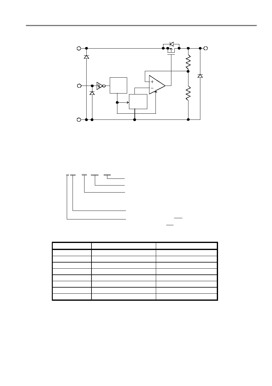
Block Diagram
Reference
voltage
VOUT
ON/OFF
VSS
VIN
*1: Parasitic diode
*1
ON/OFF
circuit
Figure 1 Block Diagram
Selection Guide
1. Product Name
S-818x xx A xx - xxx - T2
IC orientation in taping specifications
Product abbreviation
Package type
MC : SOT-23-5
UC :
A: ON/OFF pin has positive logic (high active)
B: ON/OFF pin has negative logic (low active)
SOT-89-5
Product type
Output voltage x 10
Table 1 Selection Guide
Output Voltage
SOT-23-5
SOT-89-5
2.0 V ± 2.0%
S-818A20AMC-BGA-T2
S-818A20AUC-BGA-T2
2.5 V ± 2.0%
S-818A25AMC-BGF-T2
S-818A25AUC-BGF-T2
2.8 V ± 2.0%
S-818A28AMC-BGI-T2
S-818A28AUC-BGI-T2
3.0 V ± 2.0%
S-818A30AMC-BGK-T2
S-818A30AUC-BGK-T2
3.3 V ± 2.0%
S-818A33AMC-BGN-T2
S-818A33AUC-BGN-T2
3.8 V ± 2.0%
S-818A38AMC-BGS-T2
S-818A38AUC-BGS-T2
4.0 V ± 2.0%
S-818A40AMC-BGU-T2
S-818A40AUC-BGU-T2
5.0 V ± 2.0%
S-818A50AMC-BHE-T2
S-818A50AUC-BHE-T2
Note:
Contact SII sales division for product with an output voltage other than those
specified above or product type B, low active product.
Rev.1.2
LOW DROPOUT CMOS VOLTAGE REGULATOR
S-818 Series
Seiko Instruments Inc.
3
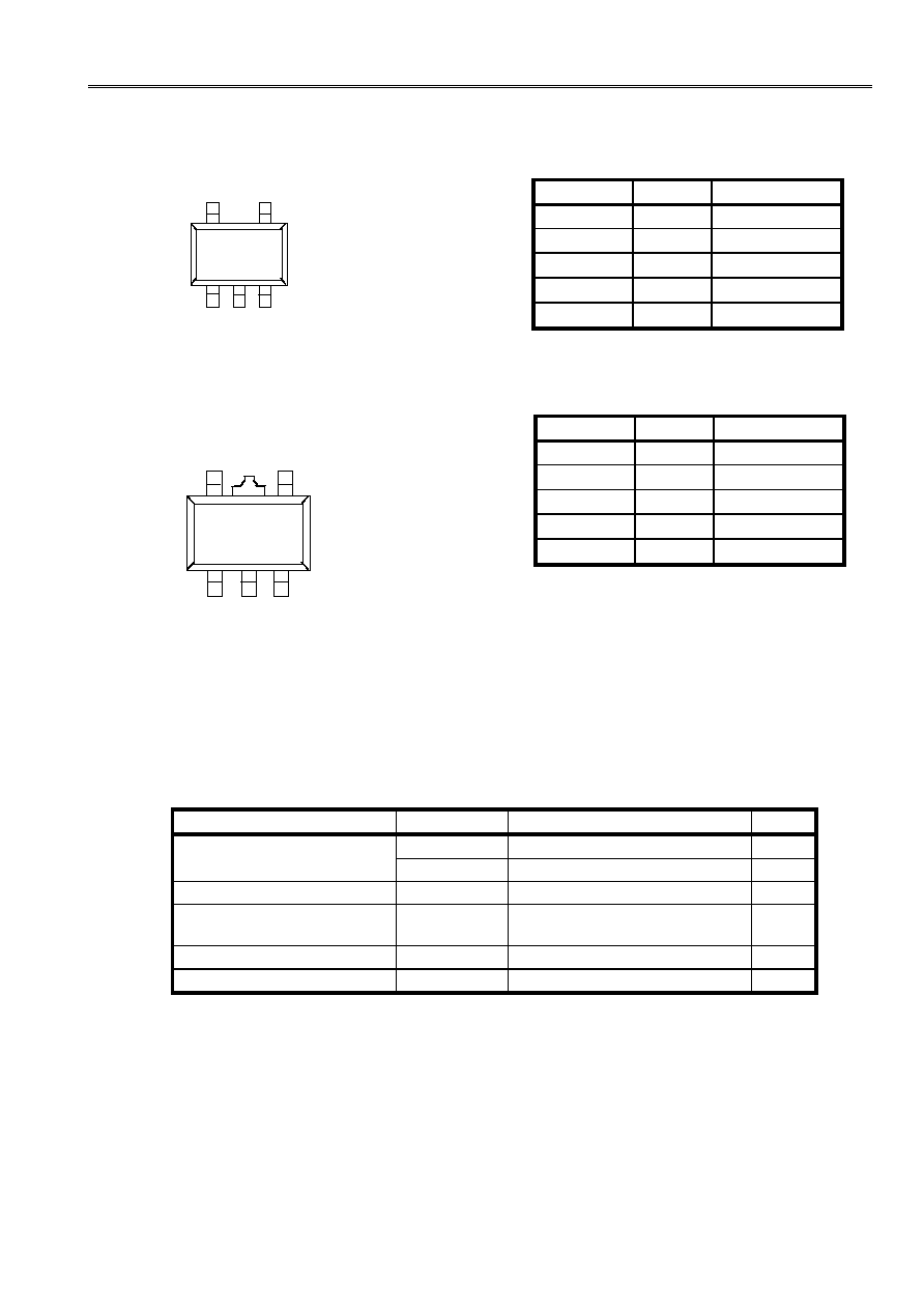
Pin Configuration
Please refer to the package drawings at the end of this document for details.
Table 2 Pin Assignment
Table 3 Pin Assignment
Note
:
NC means electrical open. Connecting
NC pin to VIN or VSS is allowed.
Absolute Maximum Ratings
Table 4 Absolute Maximum Ratings
(Ta=25
∞
C unless otherwise specified)
Parameter
Symbol
Absolute Maximum Rating
Unit
Input voltage
V
IN
12
V
V
ON / OFF
V
SS
-0.3 to 12
V
Output voltage
V
OUT
V
SS
-0.3 to V
IN
+0.3
V
Power dissipation
P
D
250 (SOT-23-5)
500 (SOT-89-5)
mW
Operating temperature range
Tope
-40 to +85
∞
C
Storage temperature range
Tstg
-40 to +125
∞
C
The IC has a protection circuit against static electricity. DO NOT apply high static electricity or high voltage
that exceeds the performance of the protection circuit to the IC.
Pin No.
Symbol
Description
1
VIN
Voltage input pin
2
VSS
GND pin
3
ON/OFF
Power off pin
4
NC
Note
No connection
5
VOUT
Voltage output pin
Figure 2 SOT-23-5
1
3
2
4
5
SOT-23-5
Top view
Pin No.
Symbol
Description
1
VOUT
Voltage output pin
2
VSS
GND pin
3
NC
Note
No connection
4
ON/OFF
Power off pin
5
VIN
Voltage input pin
5
4
1
3
2
SOT-89-5
Top view
Figure 3 SOT-89-5
LOW DROPOUT CMOS VOLTAGE REGULATOR
Rev.1.2
S-818 Series
4
Seiko Instruments Inc.
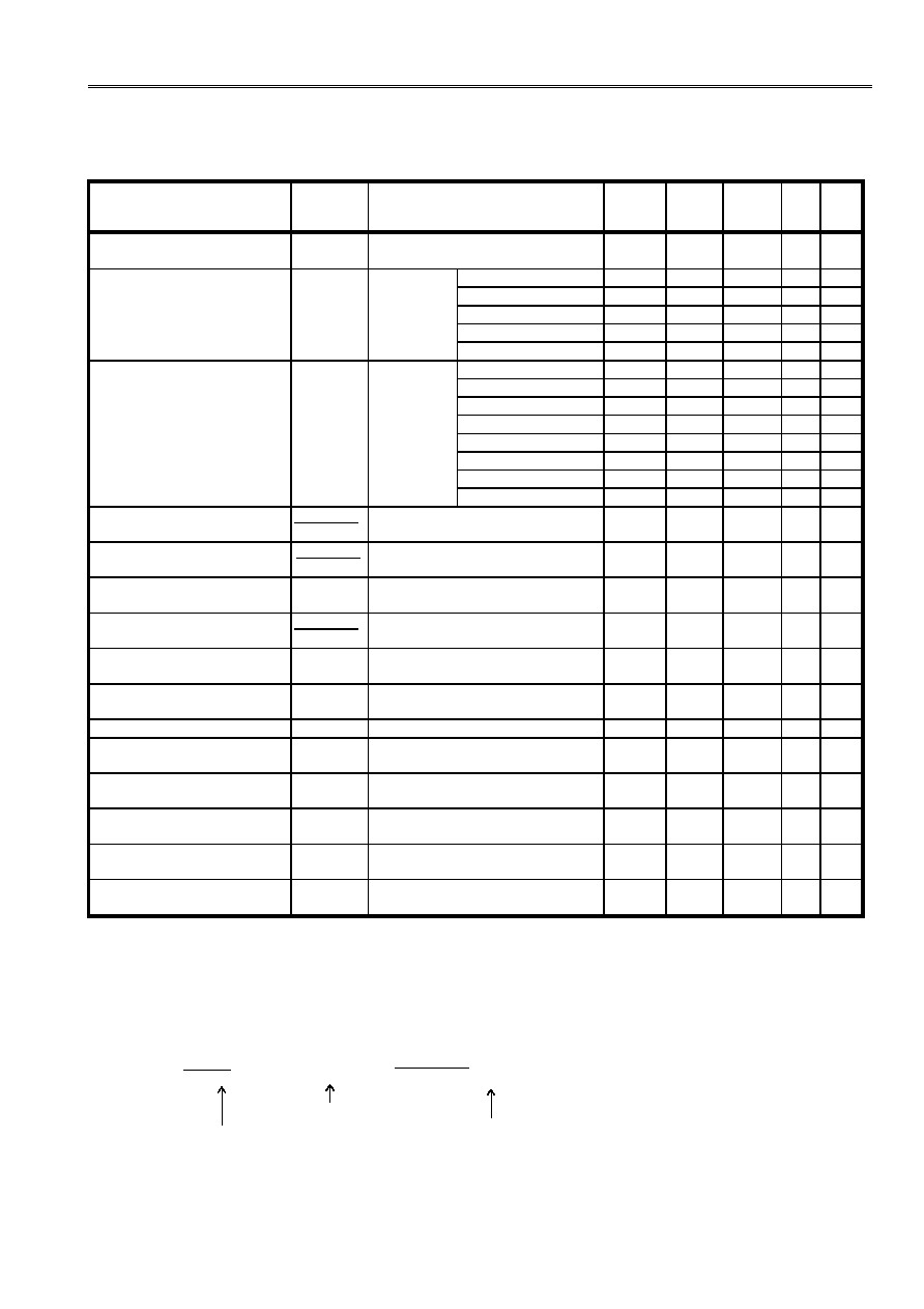
Electrical Characteristics
S-818AXXAMC/UC, S-818BXXAMC/UC
Table 5 Electrical Characteristics (Ta=25
∞
C unless otherwise specified)
Parameter
Symbol
Conditions
Min.
Typ.
Max.
Units
Test
circuit
s
Output voltage
*1)
V
OUT
(E)
V
IN
=V
OUT
(S)+1V,I
OUT
=30mA
V
OUT
(S)
◊
0.98
V
OUT
(S) V
OUT
(S)
◊
1.02
V
1
Output current
*2)
I
OUT
V
OUT
(S)+
1V
2.0V
V
OUT
(S)
2.4V
100
*5)
-
-
mA
3
V
IN
10V
2.5V
V
OUT
(S)
2.9V
150
*5)
-
-
mA
3
3.0V
V
OUT
(S)
3.9V
200
*5)
-
-
mA
3
4.0V
V
OUT
(S)
4.9V
250
*5)
-
-
mA
3
5.0V
V
OUT
(S)
6.0V
300
*5)
-
-
mA
3
Dropout voltage
*3)
Vdrop
I
OUT
=
2.0V
V
OUT
(S)
2.4V
-
0.51
0.87
V
1
60mA
2.5V
V
OUT
(S)
2.9V
-
0.38
0.61
V
1
3.0V
V
OUT
(S)
3.4V
-
0.30
0.44
V
1
3.5V
V
OUT
(S)
3.9V
-
0.24
0.33
V
1
4.0V
V
OUT
(S)
4.4V
-
0.20
0.26
V
1
4.5V
V
OUT
(S)
4.9V
-
0.18
0.22
V
1
5.0V
V
OUT
(S)
5.4V
-
0.17
0.21
V
1
5.5V
V
OUT
(S)
6.0V
-
0.17
0.20
V
1
Line regulation 1
V
OUT
1
1
V
IN
∑
V
OUT
V
OUT
(S) + 0.5 V
V
IN
10 V,
I
OUT
= 30mA
0.05
0.2
%/V
1
Line regulation 2
V
OUT
2
1
V
IN
∑
V
OUT
V
OUT
(S) + 0.5 V
V
IN
10 V,
I
OUT
= 10
µ
A
0.05
0.2
%/V
1
Load regulation
V
OUT
3
V
IN
= V
OUT
(S) + 1 V,
10
µ
A
I
OUT
80mA
30
50
mV
1
Output voltage temperature
coefficient
*4)
V
OUT
1
Ta
∑
V
OUT
V
IN
= V
OUT
(S) + 1 V, I
OUT
= 30mA
-40
∞
C
Ta
85
∞
C
±
100
ppm
/
∞
C
1
Current consumption during
operation
I
SS
1
V
IN
= V
OUT
(S) + 1 V,
ON/OFF pin = ON, no load
30
40
µ
A
2
Current consumption when
power off
I
SS
2
V
IN
= V
OUT
(S) + 1 V,
ON/OFF pin = OFF, no load
0.1
0.5
µ
A
2
Input voltage
V
IN
10
V
1
Power-off pin input voltage "H"
V
SH
V
IN
= V
OUT
(S) + 1 V, R
L
= 1k
,
Judged by V
OUT
output level.
1.5
V
4
Power-off pin input voltage "L"
V
SL
V
IN
= V
OUT
(S) + 1 V, R
L
= 1k
,
Judged by V
OUT
output level.
0.3
V
4
Power-off pin input current "H"
I
SH
V
IN
= V
OUT
(S) + 1 V,
ON/OFF = 7 V
0.1
µ
A
4
Power-off pin input current "L"
I
SL
V
IN
= V
OUT
(S) + 1 V,
ON/OFF = 0 V
-0.1
µ
A
4
Ripple rejection
RR
V
IN
= V
OUT
(S) + 1 V, f = 100Hz,
Vrip = 0.5 V p-p, I
OUT
=30mA
45
dB
5
*1) V
OUT
(S)=Specified output voltage
V
OUT
(E)=Effective output voltage, i.e., the output voltage at fixet I
OUT
(=30 mA) and input V
OUT
(S)+1.0 V.
*2) Output current when the output voltage goes below 95% of V
OUT
(E) after gradually increasing output current.
*3) Vdrop = V
IN
1-(V
OUT
(E) ◊ 0.98)
V
IN
1
= Input voltage when output voltage falls 98% of
V
OUT
(E) after gradually decreasing input voltage.
*4) Output voltage shift by temperature [mV/∞C] is calculated using the following equation.
*5) Peak output current can exceed the minimum value.
V
OUT
[ppm/
∞
C]
˜
1000
[mV/
∞
C] = V
OUT
(S)[V] ◊
Ta
V
OUT
Ta
∑
V
OUT
Specified output voltage
Output voltage temperature coefficient
Output voltage shift by temperature
Rev.1.2
LOW DROPOUT CMOS VOLTAGE REGULATOR
S-818 Series
Seiko Instruments Inc.
5
Test Circuits
1.
2.
3.
4.
5.
Figure 4 Test Circuits
Standard Circuit
VSS
VOUT
VIN
C
IN
C
L
INPUT
OUTPUT
GND
Single GND
Figure 5 Standard Circuit
Operating Conditions
Input capacitor (C
IN
)
: 0.47
µ
F or more
Output capacitor (C
L
)
: 2
µ
F or more
Equivalent Series Resistor (ESR) : 10
or less
Input Series Resistor (R
IN
)
: 10
or less
VSS
VOUT
ON/OFF
VIN
V
A
Set to
power ON
VSS
VOUT
Set to
V
IN
or GND
ON/OFF
VIN
A
VSS
R
L
VOUT
ON/OFF
VIN
V
A
VSS
VOUT
ON/OFF
VIN
V
A
Set to
power ON
VSS
VOUT
ON/ OFF
VIN
V
Set to
power ON
R
L
In addition to a tantalum capacitor, a ceramic
capacitor of 2
µ
F or more can be used in CL.
C
IN
is a capacitor used to stabilize input. Use a
capacitor of 0.47
µ
F or more.