S8231_E6.2_00

Seiko Instruments Inc.
1
Rev.6.2_
00
BATTERY PROTECTION IC (FOR A
SINGLE-CELL PACK)
S-8231 SERIES
The 8231 is a series of lithium-ion rechargeable battery protection ICs
incorporating high-accuracy voltage detection circuits and delay circuits.
It is suitable for a single-cell lithium-ion battery pack.
Features
(1) Internal high-accuracy voltage detection circuit
Overcharge detection voltage
4.00 V
± 25 mV to 4.60 V ± 25 mV
5 mV- step
Overcharge release voltage
3.70 V
± 50 mV to 4.60 V ± 50m V
5 mV- step
(The Overcharge release voltage can be selected within the range where the difference from
Overcharge detection voltage is 0 to 0.3 V)
Overdischarge detection voltage
1.70 V
± 80 mV to 2.50 V ± 80 mV
50 mV- step
Overdischarge release voltage
1.70 V
± 100 mV to 3.50 V ± 100 mV
50 mV - step
(The overdischarge release voltage can be selected within the range where a difference from
overdischarge detection voltage is 0 to 1.0V)
Overcurrent detection voltage 1
0.06 V
± 20 mV to 0.30 V ± 20 mV
5 mV-step
(2)
High input-voltage device (absolute maximum rating: 18 V)
(3) Wide operating voltage range:
1.5 V to 16 V
(4) Wide operating temperature range:
-40 to +85
°C
(5) The delay time for every detection can be set via an external capacitor.
Each delay time for Overcharge detection, Overdischarge detection, Overcurrent detection are
Proportion of hundred to ten to One. or Proportion of fifty to ten to One.
(6)
Two overcurrent detection levels (protection for short-circuiting)
(7)
Internal auxiliary over voltage detection circuit (Fail safe for over voltage)
(8)
Internal charge circuit for 0V battery (Unavailable is option)
(9)
Low current consumption
Operation 7.5
µA typ. 13.7 µA max. (-40 to +85 °C)
Power-down mode 0.2 nA typ. 0.14
µA max. (-40 to +85 °C)
(10) MSOP package (8-pin) 4.0 mm×2.95 mm
Applications
Lithium-ion rechargeable battery packs

Battery Protection IC (for a single-cell pack)
S-8231 Series
Rev.6.2_
00
Seiko Instruments Inc.
2
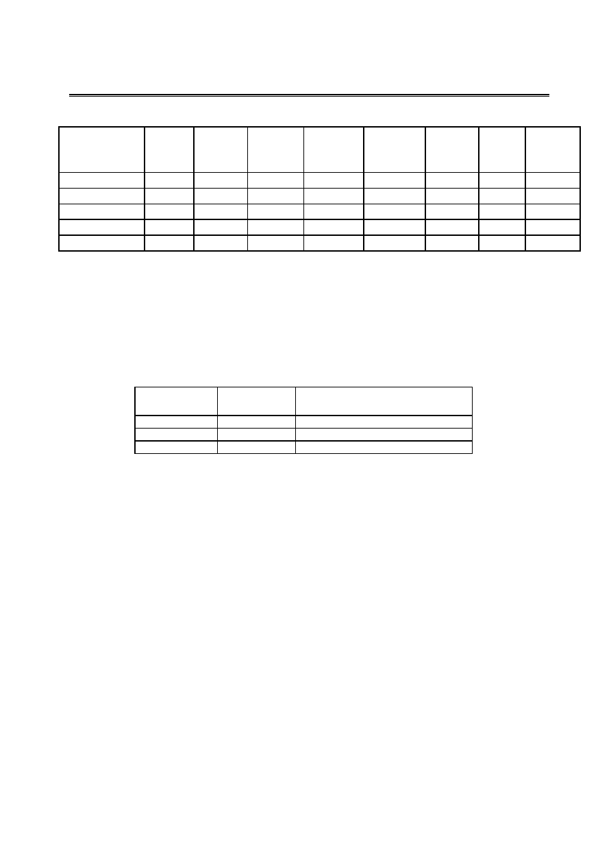
Selection Guide(6, Aug, 1999)
A / N series
Table1
Model/Item Overcharge
detection
voltage
Overcharge
release
voltage
Overdischarg
e detection
voltage
Overdischarge
release
voltage
Overcurrent
detection
voltage1
Overcharge
detection
delay
(C2=0.047
µF)
0V battery
charging
function
Auxiliary
overcharge
detection vol.
Magnification
*3
S-8231AAFN-CAA-T2 4.25V±25mV 4.05±50mV 2.30V±80mV 2.70V±100mV
0.100V±20mV 1.0
sec
Available
1.24
S-8231ABFN-CAB-T2 4.35V±25mV 4.10±50mV 2.30V±80mV 3.00V±100mV
0.100V±20mV 1.0
sec
Available
1.24
S-8231ACFN-CAC-T2 4.25V±25mV 4.05±50mV 2.30V±80mV 2.50V±100mV
0.120V±20mV 0.5
sec Unavailable
1.24
S-8231ADFN-CAD-T2 4.25V±25mV 4.05±50mV 2.30V±80mV 2.50V±100mV
0.240V±20mV 0.5
sec Unavailable
1.24
S-8231AEFN-CAE-T2 4.25V±25mV 3.95±50mV 2.30V±80mV 3.00V±100mV
0.100V±20mV 1.0
sec
Available
1.24
S-8231AGFN-CAG-T2 4.25V±25mV 4.05±50mV 2.30V±80mV 2.70V±100mV
0.150V±20mV 1.0
sec
Available
1.24
S-8231AHFN-CAH-T2 4.35V±25mV 4.28±50mV 2.30V±80mV 2.80V±100mV
0.100V±20mV 1.0
sec
Available
1.24
S-8231AIFN-CAI-T2 4.25V±25mV 4.05V
*2 2.30V±80mV
2.70V±100mV
0.150V±20mV 1.0
sec Available
1.24
S-8231AJFN-CAJ-T2 4.25V±25mV
4.05±50mV 2.30V±80mV
2.50V±100mV
0.120V±20mV 0.5
sec Available
1.24
S-8231AKFN-CAK-T2 4.25V±25mV 4.05±50mV 2.30V±80mV 2.50V±100mV
0.240V±20mV 0.5
sec
Available
1.24
S-8231ALFN-CAL-T2 4.295V±25mV 4.20±50mV 2.50V±80mV 3.00V±100mV 0.150V±20mV 1.0
sec Unavailable
1.10
S-8231AMFN-CAM-T2 4.25V±25mV 4.05±50mV 2.30V±80mV 2.70V±100mV 0.130V±20mV 1.0
sec Unavailable
1.24
S-8231ANFN-CAN-T2 4.35V±25mV 4.10±50mV 2.30V±80mV 3.00V±100mV
0.100V±20mV 0.5
sec Unavailable
1.24
S-8231AOFN-CAO-T2 4.295V±25mV 4.295V *1 2.30V±80mV 3.00V±100mV 0.300V±20mV
1.0 sec
Unavailable
1.10
S-8231AQFN-CAQ-T2 4.20V±25mV 4.10±50mV 2.30V±80mV 2.50V±100mV
0.200V±20mV 1.0
sec Unavailable
1.24
S-8231ARFN-CAR-T2 4.20V±25mV 4.10±50mV 2.30V±80mV 2.50V±100mV
0.100V±20mV 1.0
sec Unavailable
1.24
S-8231ASFN-CAS-T2 4.12V±25mV 4.12V
*1 2.30V±80mV
2.50V±100mV
0.200V±20mV 1.0
sec Unavailable
1.10
S-8231ATFN-CAT-T2 4.35V±25mV 4.10±50mV 2.30V±80mV 3.00V±100mV
0.250V±20mV 1.0
sec
Available
1.24
S-8231AUFN-CAU-T2 4.28V±25mV 4.05±50mV 2.30V±80mV 2.70V±100mV
0.130V±20mV 1.0
sec
Available
1.24
S-8231AVFN-CAV-T2 4.28V±25mV 4.05±50mV 2.30V±80mV 2.70V±100mV
0.130V±20mV 1.0
sec Unavailable
1.24
S-8231AWFN-CAW-T2 4.28V±25mV 4.18±50mV 2.30V±80mV 2.90V±100mV 0.080V±20mV 1.0
sec Unavailable
1.24
S-8231AXFN-CAX-T2 4.295V±25mV 4.295V *1 2.30V±80mV 3.00V±100mV 0.300V±20mV
1.0 sec
Unavailable
Unavailable
S-8231NAFN-CDA-T2 4.33V±25mV 4.28±50mV 2.30V±80mV 2.80V±100mV
0.100V±20mV 1.0
sec
Available
1.24
S-8231NBFN-CDB-T2 4.28V±25mV 3.98±50mV 2.30V±80mV 2.35V±100mV
0.125V±20mV 1.0
sec Unavailable
1.24
S-8231NCFN-CDC-T2 4.28V±25mV 4.18±50mV 2.30V±80mV 2.90V±100mV
0.060V±20mV 1.0
sec Unavailable
1.24
S-8231NDFN-CDD-T2 4.25V±25mV 4.05±50mV 2.30V±80mV 2.70V±100mV
0.130V±20mV 1.0
sec
Available Unavailable
S-8231NEFN-CDE-T2 4.20V±25mV 4.07±50mV 2.50V±80mV 2.75V±100mV
0.200V±20mV 1.0
sec Unavailable
1.24
Battery Protection IC (for a single-cell pack)
Rev.6.2_
00
S-8231 Series
Seiko Instruments Inc.
3
B series
Model/Item Overcharge
detection
voltage
(0 to 50°C)
Overcharge
release
voltage
Overdischarge
detection
voltage
Overdischarge
release voltage
Overcurrent
detection
voltage1
Overcharge
detection
delay
(C2=0.047
µF)
0V battery
charging
function
Auxiliary
overcharge
detection vol.
Magnification
*3
S-8231BAFN-CCA-T2 4.18V±30mV 3.98V±50mV 2.60V±80mV 2.90V±100mV 0.110V±20mV
1.0 sec
Available
1.24
S-8231BBFN-CCB-T2 4.18V±30mV 4.08V±50mV 2.30V±80mV 2.90V±100mV 0.110V±20mV
1.0 sec
Available
1.24
S-8231BGFN-CCG-T2 4.28V±30mV 4.08V±50mV 2.60V±80mV 2.90V±100mV 0.080V±20mV
1.0 sec
Unavailable
1.24
S-8231BIFN-CCI-T2 4.28V±30mV 4.08V±50mV 2.60V±80mV 2.90V±100mV 0.080V±20mV
1.0
sec
Available
1.24
S-8231BKFN-CCK-T2 4.22V±30mV 4.22V *1
2.3 0V±80mV
2.30V *4
0.200V±20mV
0.5 sec
Available
Unavailable
*1) No hysteresis is set between overcharge detection and release.
*2) Charge and discharge are prohibited once overcharge is detected. (Overcharge lock type)
*3) Auxiliary overcharge detection voltage comes in three types, i.e., overcharge detection voltage (VCU) x 1. 24 times, overcharge
detection voltage (VCU) x 1.10 times, and no final overcharge detection function.
*4) No hysteresis is set between overdischarge detection and release.
Change in the detection voltage is available in products other than the above listed ones.
Please contact with our sales division.
The overdischarge detection voltage can be selected within the range from 1.7 to 3.0V. When the
Overdischarge detection voltage is higher than 2.5V, the Overcharge detection voltage and the Overcharge
release voltage are limited as follows table.
Table 2
Overdischarge
detection voltage
(VDD)
Overcharge
detection voltage
(VCU)
Voltage difference between
Overcharge detection voltage and
Overcharge release voltage
1.70 to 2.50 V
4.00 to 4.60 V
0 to 0.30 V
1.70 to 2.70 V
4.00 to 4.50 V
0 to 0.20 V
1.70 to 3.00 V
4.00 to 4.35 V
0 to 0.10 V
Battery Protection IC (for a single-cell pack)
S-8231 Series
Rev.6.2_
00
Seiko Instruments Inc.
4
Block Diagram
Control
logic
Over discharge
Reference
voltage
Over current
detection circuit
Delay
circuit
-
+
-
+
VM
ICT
VSS
SENS
VCC
CO
DO
-
-
+
Delay circuit
control signal
Control signal
Over charge
Auxiliary
Over charge
Delay circuit
control signal
Delay circuit
control signal
RCOL
Figure 1
Output impedance when CO terminal output `L' is higher than DO terminal. Resistor (RCOL) is connected
with CO terminal. Please refer `Electric Characteristics'.
Battery Protection IC (for a single-cell pack)
Rev.6.2_
00
S-8231 Series
Seiko Instruments Inc.
5
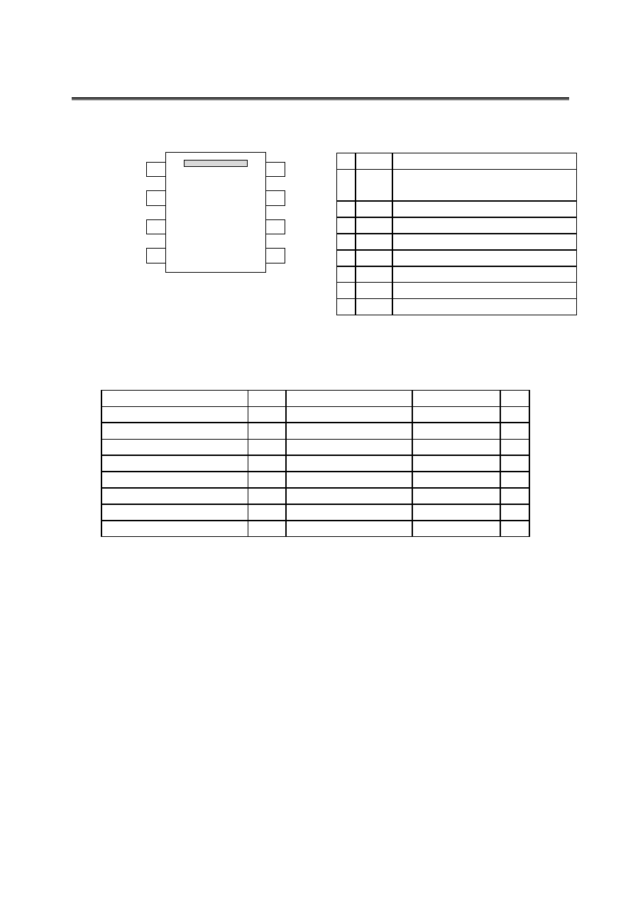
Pin Assignment
Top View
DO
ICT
NC
VSS
SENS
VCC
VM
CO
1
2
3
4
5
6
8
7
Figure 2
MSOP - 8
Pin Description
Table.3
No. Name
Description
1
SENS
Detects voltage between Vss to SENS(Overcharge/discharge
detection pin)
2
DO
Connects FET gate for discharge control (CMOS output)
3
CO
Connects FET gate for charge control (CMOS output)
4
VM
Detects voltage between VSS to VM(Overcurrent detection pin)
5
VSS
Negative power input
6
ICT
Connects capacitor for every detection delay circuit
7 NC
Non
connect
8
VCC
Positive power input and connects battery positive voltage
Absolute Maximum Ratings
Table 4
Ta = 25
°C
Item Sym.
Applied
Pins Rating
Unit
Input voltage between VCC and VSS
VDS
VCC
VSS-0.3 to VSS+18
V
ICT input terminal voltage
VICT
ICT
VSS-0.3 to VCC+0.3
V
VM input terminal voltage
VVM
VM
VCC-18 to VCC+0.3
V
DO output terminal voltage
VDO
DO
VSS-0.3 to VCC+0.3
V
CO output terminal voltage
VCO
CO
VM-0.3 to VCC+0.3
V
Power dissipation
PD
150
mW
Operating temperature range
Topr
-40 to +85
°C
Storage temperature range
Tstg
-40 to +125
°C
Document Outline
- S-8231 Series
- Cover
- Features
- Applications
- Selection Guide(6, Aug, 1999)
- Block Diagram
- Pin Assignment
- Pin description
- Absolute Maximum Ratings
- Electrical Characteristics
- Measurement Circuits
- Description of Operation
- Operation Timing Charts
- Battery Protection IC Connection Example
- Precautions
- Characteristics (typical characteristics)
- Package Drawing