Document Outline
- S-8232 Series
- Cover
- Features
- Applications
- Package
- Selection Guide (01 .Nov ,2001)
- Block Diagram
- Pin Assignment
- Pin Description
- Absolute Maximum Ratings
- Electrical Characteristics
- Measurement Circuits
- Description of Operation
- Operation Timing Charts
- Battery Protection IC Connection Example
- Precautions
- Characteristics(typical characteristics)
- Package Drawing

Rev.4.1
_00
BATTERY PROTECTION IC (FOR A 2-SERIAL-CELL PACK)
S-8232 Series
Seiko Instruments Inc.
1
The 8232 is a series of lithium-ion rechargeable battery protection
ICs incorporating high-accuracy voltage detection circuits and
delay circuits.
The S-8232 is suitable for a 2-serial-cell lithium-ion battery pack.
Features
(1)
Internal high-accuracy voltage detection circuit
Overcharge detection voltage
3.90 V
Ī 25 mV to 4.60 V Ī 25 mV
5 mV- step
Overcharge release voltage
3.60 V
Ī 50 mV to 4.60 V Ī 50 mV
5 mV- step
(The Overcharge release voltage can be selected within the range where a difference from
Overcharge detection voltage is 0 to 0.3 V)
Overdischarge detection voltage
1.70 V
Ī 80 mV to 2.60 V Ī 80 mV
50 mV- step
Overdischarge release voltage
1.70 V
Ī 100 mV to 3.80 V Ī 100 mV
50 mV - step
(The Overdischarge release voltage can be selected within the range where a difference from
Overdischarge detection voltage is 0 to 1.2 V)
Overcurrent detection voltage 1
0.07 V
Ī 20 mV to 0.30 V Ī 20 mV
5 mV-step
(2)
High input-voltage device (absolute maximum rating: 18 V)
(3)
Wide operating voltage range:
2.0 V to 16 V
(4)
The delay time for every detection can be set via an external capacitor.
Each delay time for Overcharge detection, Overdischarge detection, Overcurrent detection are
"Proportion of hundred to ten to one."
(5)
Two overcurrent detection levels (protection for short-circuiting)
(6)
Internal auxiliary over voltage detection circuit (Fail safe for over voltage)
(7)
Internal charge circuit for 0 V battery (Unavailable is option)
(8)
Low current consumption
Operation
7.5
ĶA typ. 14.2 ĶA max (-40 to +85 įC)
Power-down mode
0.2 nA typ. 0.1
ĶA max (-40 to +85 įC)
(9)
TSSOP package (8-pin) 6.4 mm◊3.1 mm
Applications
Lithium-ion rechargeable battery packs
Package
8-PinTSSOP (PKG code:FT008-A)

Battery Protection IC (for a 2-serial-cell pack)
S-8232 Series
Rev. 4.1
_00
2
Seiko Instruments Inc.
Selection Guide (01 .Nov ,2001)
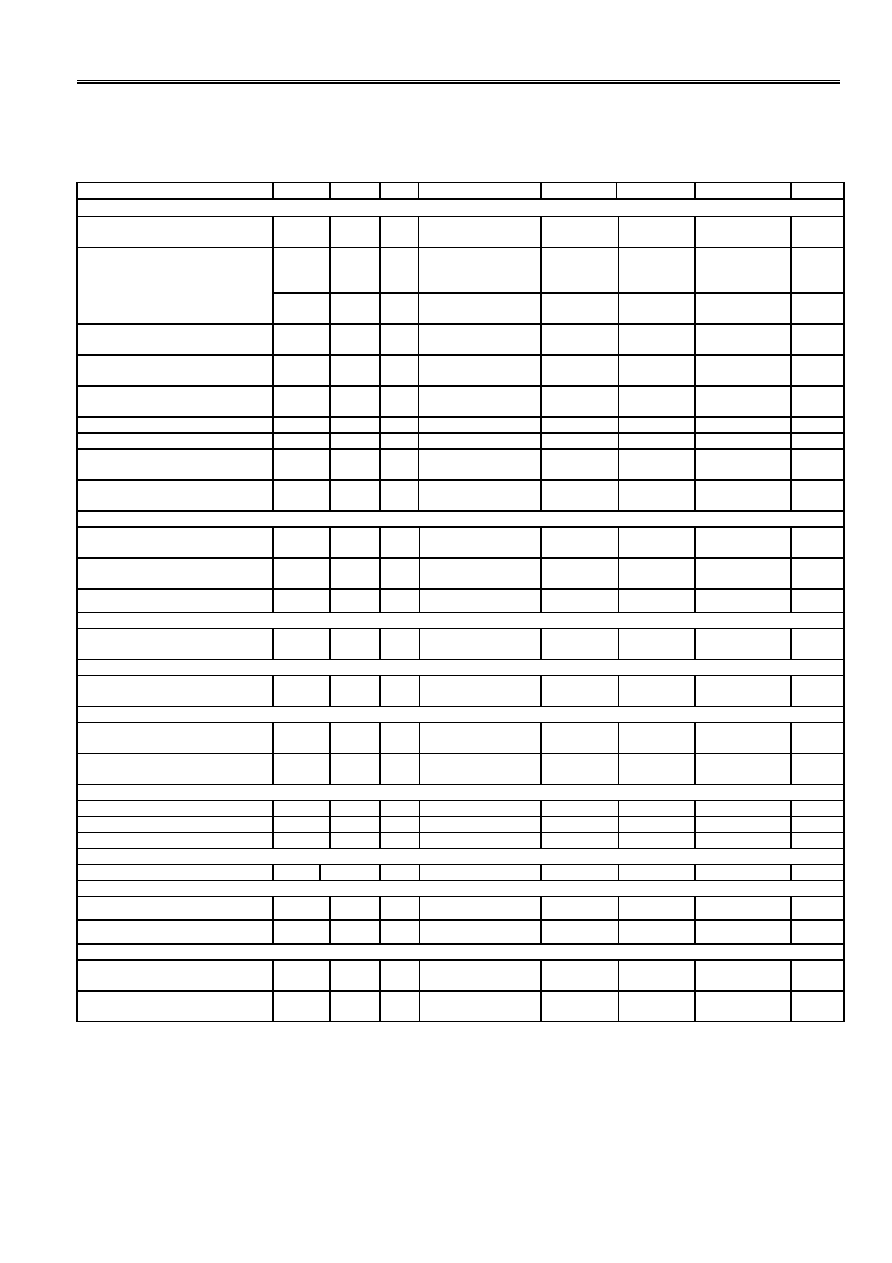
Table1
Model/Item
Overcharge
detection
voltage1,2
(V
CU1,2
)
Overcharge
release voltage1,2
(V
CD1,2
)
Overdischarge
detection
voltage1,2
(V
DD1,2
)
Overdischarge
release
voltage1,2
(V
DU1,2
)
Overcurrent
detection
voltage1
(V
IOV1
)
Overcharge
detection delay
time (t
CU
)
C3=0.22
Ķ
F
0 V battery
charging
function
S-8232AAFT 4.25VĪ25mV 4.05Ī50mV 2.40VĪ80mV
3.00VĪ100mV
0.150VĪ20mV 1.0
s
Available
S-8232ABFT 4.35VĪ25mV 4.15Ī50mV 2.30VĪ80mV
3.00VĪ100mV
0.300VĪ20mV 1.0
s
Available
S-8232ACFT 4.35VĪ25mV
4.15Ī50mV 2.30VĪ80mV
3.00VĪ100mV
0.300VĪ20mV 1.0
s Unavailable
S-8232AEFT 4.35VĪ25mV 4.28Ī50mV 2.15VĪ80mV
2.80VĪ100mV
0.100VĪ20mV 1.0
s
Available
S-8232AFFT 4.25VĪ25mV 4.05Ī50mV 2.30VĪ80mV
2.70VĪ100mV
0.300VĪ20mV 1.0
s
Available
S-8232AGFT 4.25VĪ25mV
4.05Ī50mV 2.20VĪ80mV
2.40VĪ100mV
0.200VĪ20mV 1.0
s
Available
S-8232AHFT 4.25VĪ25mV
4.05Ī50mV 2.20VĪ80mV
2.40VĪ100mV
0.300VĪ20mV 1.0
s
Available
S-8232AIFT 4.325VĪ25mV 4.325VĪ25mV
1),2)
2.40VĪ80mV 3.00VĪ100mV 0.300VĪ20mV
1.0
s
Unavailable
S-8232AJFT 4.25VĪ25mV 4.05Ī50mV 2.40VĪ80mV
3.00VĪ100mV
0.150VĪ20mV 1.0
s Unavailable
S-8232AKFT 4.20VĪ25mV 4.00Ī50mV 2.30VĪ80mV
2.90VĪ100mV
0.200VĪ20mV 1.0
s
Available
S-8232ALFT 4.30VĪ25mV 4.05Ī50mV 2.00VĪ80mV
3.00VĪ100mV
0.200VĪ20mV 1.0
s
Available
S-8232AMFT 4.19VĪ25mV 4.19
VĪ25mV
1)
2.00VĪ80mV 3.00VĪ100mV
0.190VĪ20mV 1.0
s
Available
S-8232ANFT 4.325VĪ25mV 4.325VĪ25mV
1),3)
2.40VĪ80mV 3.00VĪ100mV 0.300VĪ20mV
1.0
s
Unavailable
S-8232AOFT 4.30VĪ25mV
4.05Ī50mV 2.00VĪ80mV
3.00VĪ100mV
0.230VĪ20mV 1.0
s
Available
S-8232APFT 4.28VĪ25mV 4.05Ī50mV 2.30VĪ80mV
2.90VĪ100mV
0.100VĪ20mV 1.0
s Unavailable
S-8232ARFT 4.325VĪ25mV 4.325VĪ25mV
1),3)
2.00VĪ80mV 2.50VĪ100mV 0.300VĪ20mV
1.0
s
Unavailable
S-8232ASFT
4)
4.295VĪ25mV 4.20Ī50mV
3)
2.30VĪ80mV
3.00VĪ100mV
0.300VĪ20mV 1.0
s Unavailable
S-8232ATFT 4.125VĪ25mV 4.125Ī25mV
1)
2.00VĪ80mV 3.00VĪ100mV
0.190VĪ20mV 1.0
s
Available
S-8232AUFT 4.30VĪ25mV
4.10Ī50mV 2.40VĪ80mV
3.00VĪ100mV
0.200VĪ20mV 1.0
s Unavailable
S-8232AVFT 4.30VĪ25mV 4.05VĪ50mV 2.00VĪ80mV
3.00VĪ100mV
0.300VĪ20mV 1.0
s
Available
S-8232AWFT 4.35VĪ25mV 4.15VĪ50mV 2.30VĪ80mV
3.00VĪ100mV
0.150VĪ20mV 1.0
s Unavailable
S-8232AXFT 4.325VĪ25mV 4.200VĪ50mV 2.30VĪ80mV
3.00VĪ100mV
0.20VĪ20mV 1.0
s Unavailable
S-8232AYFT 4.30VĪ25mV 4.05VĪ50mV 2.00VĪ80mV
2.00VĪ80mV
0.20VĪ20mV 1.0
s
Available
S-8232AZFT 4.30VĪ25mV 4.05VĪ50mV 2.30VĪ80mV
2.30VĪ80mV
0.20VĪ20mV 1.0
s
Available
S-8232NAFT 4.325VĪ25mV 4.325VĪ25mV
1), 3)
2.40VĪ80mV 3.00VĪ100mV 0.15VĪ20mV
1.0
s
Unavailable
S-8232NCFT
4.275 VĪ25 mV
4.05 VĪ50 mV
2.20 VĪ80 mV 3.00 VĪ100 mV 0.20 VĪ20 mV
1.0 s
Unavailable
S-8232NDFT
4.35 VĪ25 mV
4.15 VĪ50 mV
2.30 VĪ80 mV 2.30 VĪ80 mV 0.15 VĪ20 mV
1.0 s
Available
1): No overcharge detection/release hysteresis
2): The magnification of final overcharge is 1.11; other is 1.25.
3): No final overcharging function
4): Refer to the Description of Operation (*3).
Change in the detection voltage is available. Please contact SII sales office.
The overdischarge detection voltage can be selected within the range from 1.7 to 3.0 V.
When the overdischarge detection voltage is higher than 2.6 V, the overcharge detection voltage and the
overcharge release voltage are limited as table 2.
Table 2
Overdischarge detection
voltage1,2 (V
DD1,2
)
Overcharge detection
voltage1,2 (V
CU1,2
)
Voltage difference between overcharge detection voltage
and overcharge release voltage (V
CU1,2
- V
CD1,2
)
1.70 to 2.60 V
3.90 to 4.60 V
0 to 0.30 V
1.70 to 2.80 V
3.90 to 4.60 V
0 to 0.20 V
1.70 to 3.00 V
3.90 to 4.50 V
0 to 0.10 V

Battery Protection IC (for a 2-serial-cell pack)
Rev. 4.1
_00
S-8232 Series
Seiko Instruments Inc.
3
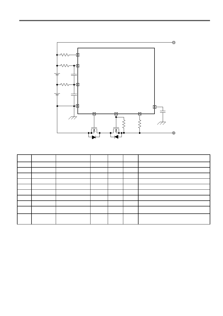
Block Diagram
Auxiliary
Over charge
detector 2
Over charge
detector 2
Delay circuit
control signal
Delay circuit
control signal
Delay circuit
control signal
Auxiliary
Over
charge
detector 1
Reference
voltage 2
Reference
voltage 1
Control
Logic
DO,CO control signal
-
+
Over current
detection
circuit
CO
DO
ICT
VM
VSS
VC
SENS
VCC
Delay circuit
Over charge
detector 1
Delay circuit
control signal
Over discharge
detector 1
Over discharge
detector 2
R
COL
-
+
-
-
+
+
-
+
-
+
Figure 1
Output impedance when CO terminal output `L' is higher than DO terminal. R
COL
resistor is connected with CO
terminal. Please refer `Electric Characteristics'.

Battery Protection IC (for a 2-serial-cell pack)
S-8232 Series
Rev. 4.1
_00
4
Seiko Instruments Inc.
Pin Assignment
Top View
1
2
3
4
8
7
6
5
TSSOP-8
Figure 2
Pin Description
Table
3
No. Name
Description
1 SENS
Detection pin for voltage between SENS and VC (Detection for
overcharge and overdischarge)
2
DO
FET gate connection pin for discharge control (CMOS output)
3
CO
FET gate connection pin for charge control (CMOS output)
4
VM
Detection pin for voltage between VM and VSS (Overcurrent detection
pin)
5
VSS
Negative power input pin
6
ICT
Capacitor connection pin for detection delay
7
VC
Middle voltage input pin
8
VCC
Positive power input pin
Absolute Maximum Ratings
Table 4
Ta
= 25įC
Item Symbol
Applied
Pins Rating
Unit
Input voltage between VCC and VSS
V
DS
VCC V
SS
-0.3 to V
SS
+18 V
SENS Input terminal voltage
V
SENS
SENS V
SS
-0.3 to V
CC
+0.3 V
ICT Input terminal voltage
V
ICT
ICT V
SS
-0.3 to V
CC
+0.3 V
VM Input terminal voltage
V
VM
VM V
CC
-18 to V
CC
+0.3 V
DO output terminal voltage
V
DO
DO V
SS
-0.3 to V
CC
+0.3 V
CO output terminal voltage
V
CO
CO V
VM
-0.3 to V
CC
+0.3 V
Power dissipation
P
D
300
mW
Operating temperature range
T
opr
-40 to +85 įC
Storage temperature range
T
stg
-40 to +125 įC
Battery Protection IC (for a 2-serial-cell pack)
Rev. 4.1
_00
S-8232 Series
Seiko Instruments Inc.
5
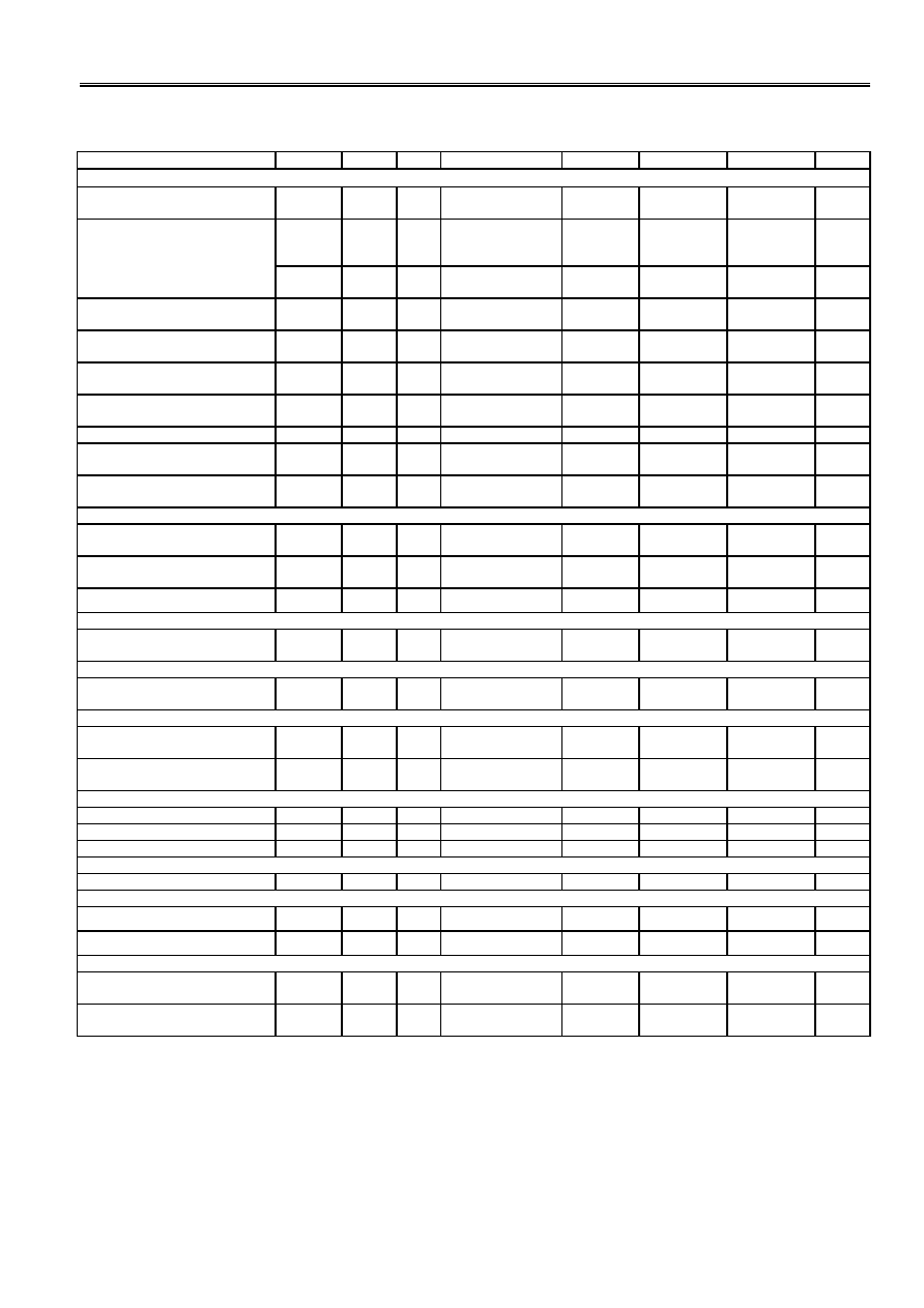
Electrical Characteristics
Table 5
Unless otherwise noted, Ta
= 25įC
Item
Symbol Condition
Circuit
Notice Min.
Typ.
Max.
Unit
Detection voltage
Overcharge detection voltage 1,2
V
CU1,2
1,2 1 Between
3.90
and
4.60
V
CU1,2
-0.025
V
CU1,2
V
CU1,2
+0.025
V
Auxiliary overcharge detection
voltage 1,2
(4)
V
CUaux
1,2
= V
CU1,2
◊1.25
V
CUaux1,2
1,2 1
V
CU1,2
◊1.25 V
CU1,2
◊1.21
V
CU1,2
◊1.25
V
CU1,2
◊1.29
V
or
V
CUaux
1,2
= V
CU1,2
◊1.11
V
CUaux1,2
1,2 1
V
CU1,2
◊1.11 V
CU1,2
◊1.07
V
CU1,2
◊1.11
V
CU1,2
◊1.15
V
Overcharge release voltage 1,2
V
CD1,2
1,2 1 Between
3.60
and
4.60
V
CD1,2
-0.050
V
CD1,2
V
CD1,2
+0.050
V
Overdischarge detection voltage
1,2
V
DD1,2
1,2 1 Between
1.70
and
2.60
V
DD1,2
-0.080
V
DD1,2
V
DD1,2
+0.080
V
Overdischarge release voltage 1,2
V
DU1,2
1,2 1 Between
1.70
and
3.80
V
DU1,2
-0.100
V
DU1,2
V
DU1,2
+0.100
V
Overcurrent detection voltage 1
V
IOV1
3
1
Between 0.07 to 0.30 V
IOV1
-0.020 V
IOV1
V
IOV1
+0.020 V
Overcurrent detection voltage 2
V
IOV2
3 1 V
CC
Reference
-1.57
-1.20
-0.83 V
Temperature coefficient 1 for
detection voltage
(1)
T
COE1
Ta
=-40 to 85įC
-0.6 0 0.6
mV/įC
Temperature coefficient 2 for
detection voltage
(2)
T
COE2
Ta
=-40 to 85įC
-0.24
-0.05 0
mV/įC
Delay time (C3=0.22
Ķ
Ķ
Ķ
ĶF)
Overcharge detection
delay time1,2
t
CU1,2
8,9 5
1.0
s
0.73 1.00 1.35
s
Overdischarge detection
delay time 1,2
t
DD1,2
8,9 5
0.1
s
68 100 138
ms
Overcurrent detection delay time1
t
IOV1
10 5
0.01
s
6.7 10 13.9
ms
Input voltage
Input voltage between
VCC and VSS
V
DS
Absolute
maximum
rating
-0.3
- 18
Operating voltage
Operating voltage between VCC
and VSS
(3)
V
DSOP
2.0
- 16
V
Current consumption
Current consumption
during normal operation
I
OPE
4 2 V1
=V2=3.6 V
2.1
7.5
12.7
ĶA
Current consumption
at power down
I
PDN
4 2 V1
=V2=1.5 V
0
0.0002
0.04
ĶA
Output voltage
DO"H"voltage V
DO(H)
6 3
Iout
=10 ĶA V
CC
-0.05 V
CC
-0.003 V
CC
V
DO"L"voltage V
DO(L)
6 3 Iout
=10 ĶA V
SS
V
SS
+0.003 V
SS
+0.05 V
CO"H"voltage V
CO(H)
7 4
Iout
=10 ĶA V
CC
-0.15 V
CC
-0.019 V
CC
V
CO pin internal resistance
Resistance between VSS and CO
R
COL
7 4 V
CO
-V
SS
=9.4 V
0.29
0.6
1.44
M
Internal resistance
Resistance between VCC and VM
R
vcm
5 2 Vcc
-V
VM
=0.5 V
105 240 575
k
Resistance between VSS and VM
R
vsm
5 2 V
VM
-V
SS
=1.1 V
511 597 977
k
0 V battery charging function
0 V charge starting voltage
V
0CHA
11
6
0 V battery charging
Available
0.38 0.75 1.12 V
0 V charge inhibiting voltage 1,2
V
0INH1,2
12,13
6
0 V battery charging
Unavailable
0.32 0.88 1.44 V
(1)
Temperature coefficient 1 for detection voltage should be applied to overcharge detection voltage, overcharge release
voltage, overdischarge detection voltage, and overdischarge release voltage.
(2)
Temperature coefficient 2 for detection voltage should be applied to overcurrent detection voltage.
(3)
The DO and CO pin logic are established at the operating voltage.
(4)
Auxiliary overcharge detection voltage is equal to the overcharge detection voltage times 1.11 for the products without
overcharge hysteresis, and times 1.25 for other products.

Battery Protection IC (for a 2-serial-cell pack)
S-8232 Series
Rev. 4.1
_00
6
Seiko Instruments Inc.
Table 6
Unless otherwise noted, Ta
= -20 to +70įC
Item
Symbol Condition
Circuit
Notice Min.
Typ. Max.
Unit
Detection voltage
Overcharge detection voltage 1,2
V
CU1,2
1,2
1
Between 3.90 and
4.60
V
CU1,2
-0.045
V
CU1,2
V
CU1,2
+0.040
V
Auxiliary overcharge detection
voltage 1,2
(4)
V
CUaux1,2
= V
CU1,2
◊1.25
V
CUaux1,2
1,2 1
V
CU1,2
◊1.25 V
CU1,2
◊1.19
V
CU1,2
◊1.25
V
CU1,2
◊1.31
V
or
V
CUaux1,2
= V
CU1,2
◊1.11
V
CUaux1,2
1,2 1
V
CU1,2
◊1.11 V
CU1,2
◊1.05
V
CU1,2
◊1.11
V
CU1,2
◊1.17
V
Overcharge release voltage 1,2
V
CD1,2
1,2
1
Between 3.60 and
4.60
V
CD1,2
-0.070
V
CD1,2
V
CD1,2
+0.065
V
Overdischarge detection voltage
1,2
V
DD1,2
1,2
1
Between 1.70 and
2.60
V
DD1,2
-0.100
V
DD1,2
V
DD1,2
+0.095
V
Overdischarge release voltage 1,2
V
DU1,2
1,2
1
Between 1.70 and
3.80
V
DU1,2
-0.120
V
DU1,2
V
DU1,2
+0.115
V
Overcurrent detection voltage 1
V
IOV1
3
1
Between 0.07 to
0.30
V
IOV1
-0.029 V
IOV1
V
IOV1
+0.029 V
Overcurrent detection voltage 2
V
IOV2
3 1 V
CC
Reference
-1.66
-1.20
-0.74 V
Temperature coefficient 1 for
detection voltage
(1)
T
COE1
Ta
=-40 to 85įC
-0.6 0 0.6
mV/įC
Temperature coefficient 2 for
detection voltage
(2)
T
COE2
Ta
=-40 to 85įC
-0.24
-0.05 0
mV/įC
Delay time (C3=0.22
Ķ
Ķ
Ķ
ĶF)
Overcharge detection
delay time1,2
t
CU1,2
8,9 5
1.0
s
0.60 1.00 1.84
s
Overdischarge detection
delay time 1,2
t
DD1,2
8,9 5
0.1
s
67 100 141
ms
Overcurrent detection delay time1
t
IOV1
10 5
0.01
s
6.5 10 14.5
ms
Input voltage
Input voltage between
VCC and VSS
V
DS
Absolute
maximum
rating
-0.3
- 18
Operating voltage
Operating voltage between VCC
and VSS
(3)
V
DSOP
2.0
- 16
V
Current consumption
Current consumption
during normal operation
I
OPE
4 2 V1
=V2=3.6 V
1.9
7.5
13.8
ĶA
Current consumption
at power down
I
PDN
4 2 V1
=V2=1.5 V
0
0.0002
0.06
ĶA
Output voltage
DO"H"voltage V
DO(H)
6 3 Iout
=10 ĶA V
CC
-0.14 V
CC
-0.003 V
CC
V
DO"L"voltage V
DO(L)
6 3 Iout
=10 ĶA V
SS
V
SS
+0.003 V
SS
+0.14 V
CO"H"voltage V
CO(H)
7 4 Iout
=10 ĶA V
CC
-0.24 V
CC
-0.019 V
CC
V
CO pin internal resistance
Resistance between VSS and CO
R
COL
7 4 V
CO
-V
SS
=9.4 V
0.24
0.6
1.96
M
Internal resistance
Resistance between VCC and VM
R
vcm
5 2
V
CC
-V
VM
=0.5 V
86 240 785
k
Resistance between VSS and VM
R
vsm
5 2
V
VM
-V
SS
=1.1 V
418 597 1332
k
0 V battery charging function
0 V charge starting voltage
V
0CHA
11
6
0 V battery charging
Available
0.29 0.75 1.21 V
0 V charge inhibiting voltage 1,2
V
0INH1,2
12,13
6
0 V battery charging
Unavailable
0.23 0.88 1.53 V
(1)
Temperature coefficient 1 for detection voltage should be applied to overcharge detection voltage, overcharge release
voltage, overdischarge detection voltage, and overdischarge release voltage.
(2)
Temperature coefficient 2 for detection voltage should be applied to overcurrent detection voltage.
(3)
The DO and CO pin logic are established at the operating voltage.
(4)
Auxiliary overcharge detection voltage is equal to the overcharge detection voltage times 1.11 for the products without
overcharge hysteresis, and times 1.25 for other products.
Battery Protection IC (for a 2-serial-cell pack)
Rev. 4.1
_00
S-8232 Series
Seiko Instruments Inc.
7
Table 7
Unless otherwise noted, Ta
= -40 to +85įC
Item
Symbol Condition
Circuit
Notice Min.
Typ. Max.
Unit
Detection voltage
Overcharge detection voltage 1,2
V
CU1,2
1,2
1
Between 3.90 and
4.60
V
CU1,2
-0.055
V
CU1,2
V
CU1,2
+0.045
V
Auxiliary overcharge detection
voltage 1,2
(4)
V
CUaux1,2
= V
CU1,2
◊1.25
V
CUaux1,2
1,2 1
V
CU1,2
◊1.25 V
CU1,2
◊1.19
V
CU1,2
◊1.25
V
CU1,2
◊1.31
V
or
V
CUaux1,2
= V
CU1,2
◊1.11
V
CUaux1,2
1,2 1
V
CU1,2
◊1.11 V
CU1,2
◊1.05
V
CU1,2
◊1.11
V
CU1,2
◊1.17
V
Overcharge release voltage 1,2
V
CD1,2
1,2
1
Between 3.60 and
4.60
V
CD1,2
-0.080
V
CD1,2
V
CD1,2
+0.070
V
Overdischarge detection voltage
1,2
V
DD1,2
1,2
1
Between 1.70 and
2.60
V
DD1,2
-0.110
V
DD1,2
V
DD1,2
+0.100
V
Overdischarge release voltage 1,2
V
DU1,2
1,2
1
Between 1.70 and
3.80
V
DU1,2
-0.130
V
DU1,2
V
DU1,2
+0.120
V
Overcurrent detection voltage 1
V
IOV1
3
1
Between 0.07 to
0.30
V
IOV1
-0.033 V
IOV1
V
IOV1
+0.033 V
Overcurrent detection voltage 2
V
IOV2
3 1 V
CC
Reference
-1.70
-1.20
-0.71 V
Temperature coefficient 1 for
detection voltage
(1)
T
COE1
Ta
=-40 to 85įC
-0.6 0 0.6
mV/įC
Temperature coefficient 2 for
detection voltage
(2)
T
COE2
Ta
=-40 to 85įC
-0.24
-0.05 0
mV/įC
Delay time (C3=0.22
Ķ
Ķ
Ķ
ĶF)
Overcharge detection
delay time1,2
t
CU1,2
8,9 5
1.0
s
0.55 1.00 2.06
s
Overdischarge detection
delay time 1,2
t
DD1,2
8,9 5
0.1
s
67 100 141
ms
Overcurrent detection delay time1
t
IOV1
10 5
0.01
s
6.3 10 14.7
ms
Input voltage
Input voltage between
VCC and VSS
V
DS
Absolute
maximum
rating
-0.3
- 18
Operating voltage
Operating voltage between VCC
and VSS
(3)
V
DSOP
2.0
- 16
V
Current consumption
Current consumption
during normal operation
I
OPE
4 2 V1
=V2=3.6 V
1.8
7.5
14.2
ĶA
Current consumption
at power down
I
PDN
4 2 V1
=V2=1.5 V
0
0.0002
0.10
ĶA
Output voltage
DO"H"voltage V
DO(H)
6 3 Iout
=10 ĶA V
CC
-0.17 V
CC
-0.003 V
CC
V
DO"L"voltage V
DO(L)
6 3 Iout
=10 ĶA V
SS
V
SS
+0.003 V
SS
+0.17 V
CO"H"voltage V
CO(H)
7 4 Iout
=10 ĶA V
CC
-0.27 V
CC
-0.019 V
CC
V
CO pin internal resistance
Resistance between VSS and CO
R
COL
7 4 V
CO
-V
SS
=9.4 V
0.22
0.6
2.20
M
Internal resistance
Resistance between VCC and VM
R
vcm
5 2
Vcc
-V
VM
=0.5 V
79 240 878
k
Resistance between VSS and VM
R
vsm
5 2
V
VM
-V
SS
=1.1 V
387 597 1491
k
0 V battery charging function
0 V charge starting voltage
V
0CHA
11
6
0 V battery charging
Available
0.26 0.75 1.25 V
0 V charge inhibiting voltage 1,2
V
0INH1,2
12,13
6
0 V battery charging
Unavailable
0.20 0.88 1.57 V
(1)
Temperature coefficient 1 for detection voltage should be applied to overcharge detection voltage, overcharge release
voltage, overdischarge detection voltage, and overdischarge release voltage.
(2)
Temperature coefficient 2 for detection voltage should be applied to overcurrent detection voltage.
(3)
The DO and CO pin logic are established at the operating voltage.
(4)
Auxiliary overcharge detection voltage is equal to the overcharge detection voltage times 1.11 for the products without
overcharge hysteresis, and times 1.25 for other products.

Battery Protection IC (for a 2-serial-cell pack)
S-8232 Series
Rev. 4.1
_00
8
Seiko Instruments Inc.
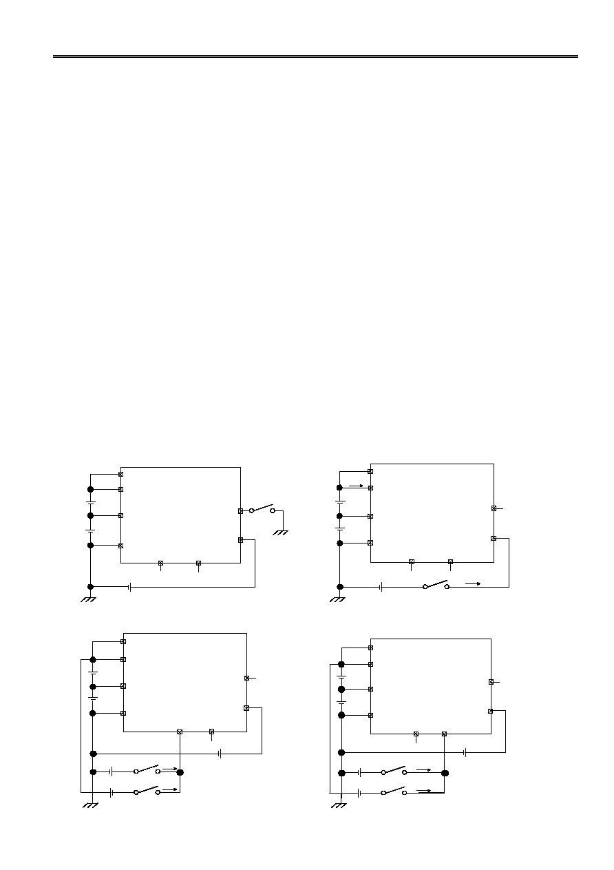
Measurement Circuits
(1) Measurement 1 Measurement circuit 1
Set S1
=OFF, V1=V2=3.6 V, and V3=0 V under normal condition. Increase V1 from 3.6 V gradually. The V1
voltage when CO
= 'L' is overcharge detection voltage 1 (V
CU1
). Decrease V1 gradually. The V1 voltage when
CO
= 'H' is overcharge release voltage 1 (V
CD1
). Further decrease V1. The V1 voltage when DO
= 'L' is
overdischarge voltage 1 (V
DD1
). Increase V1 gradually. The V1 voltage when DO
= 'H' is overdischarge
release voltage 1 (V
DU1
). Set S1
=ON, and V1=V2=3.6 V and V3=0 V under normal condition. Increase V1 from
3.6 V gradually. The V1 voltage when CO
= 'L' is auxiliary overcharge detection voltage 1 (V
CUaux1
).
(2) Measurement 2 Measurement circuit 1
Set S1
=OFF,V1=V2=3.6 V ,and V3=0 V under normal condition. Increase V2 from 3.6 V gradually. The V2
voltage when CO
= 'L' is overcharge detection voltage 2 (V
CU2
). Decrease V2 gradually. The V2 voltage when
CO
= 'H' is overcharge release voltage 2 (V
CD2
). Further decrease V2. The V2 voltage when DO
= 'L' is
overdischarge voltage 2 (V
DD2
). Increase V2 gradually. The V2 voltage when DO
= 'H' is overdischarge
release voltage 2 (V
DU2
). Set S1
=ON,and V1=V2=3.6 V and V3=0 V under normal condition. Increase V2 from
3.6 V gradually. The V2 voltage when CO
= 'L' is auxiliary overcharge detection voltage 2 (V
CUaux2
).
(3) Measurement 3 Measurement circuit 1
Set S1
=OFF,V1=V2=3.6 V , and V3=0 V under normal condition. Increase V3 from 0 V gradually. The V3
voltage when DO
= 'L' is overcurrent detection voltage 1 (V
IOV1
). Set S1
=ON,V1=V2=3.6 V,V3=0 under normal
condition. Increase V3 from 0 V gradually.(The voltage change rate < 1.0V/ms) (V1
+V2-V3) voltage when DO
= 'L' is overcurrent detection voltage 2 (V
IOV2
).
(4) Measurement 4 Measurement circuit 2
Set S1
=ON, V1=V2=3.6 V, and V3=0 V under normal condition and measure current consumption. Current
consumption I1 is the normal condition current consumption (I
OPE
). Set S1
=OFF, V1=V2=1.5 V under
overdischarge condition and measure current consumption. Current consumption I1 is the power-down
current consumption (I
PDN
).
(5) Measurement 5 Measurement circuit 2
Set S1
=ON, V1=V2=V3=1.5 V, and V3=2.5 V under overdischarge condition. (V1+V2-V3)/I2 is the internal
resistance between VCC and VM (R
vcm
).
Set S1
=ON, V1=V2=3.5 V, and V3=1.1 V under overcurrent condition. V3/I2 is the internal resistance
between VSS and VM (R
vsm
).
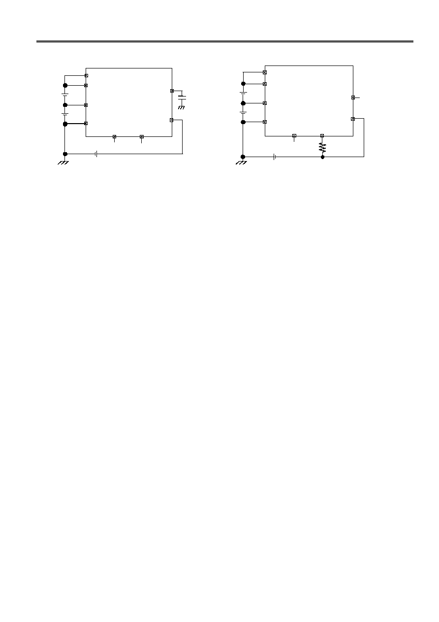
(6) Measurement 6 Measurement circuit 3
Set S1
=ON, S2=OFF, V1=V2=3.6 V, and V3=0 V under normal condition. Increase V4 from 0 V gradually.
The V4 voltage when I1
= 10 ĶA is DO'H' voltage (V
D0 (H)
).
Set S1
=OFF, S2=ON, V1=V2=3.6 V, and V3=0.5 V under overcurrent condition. Increase V5 from 0 V
gradually. The V5 voltage when I2
= 10 ĶA is the DO'L' voltage (V
DO (L)
).
(7) Measurement 7 Measurement circuit 4
Set S1
=ON, S2=OFF, V1=V2=3.6 V and V3=0 V under normal condition. Increase V4 from 0 V gradually.
The V4 voltage when I1
= 10 ĶA is the CO'H' voltage (V
C0 (H)
).
Set S1
=OFF S2=ON, V1=V2=4.7, V3=0 V, and V4=9.4 V under over voltage condition. (V5)/I2 is the CO pin
internal resistance (R
COL
).
(8) Measurement 8 Measurement circuit 5
Set V1
=V2=3.6 V, and V3=0 V under normal condition. Increase V1 from (V
CU1
-0.2 V) to (V
CU1
+0.2 V)
immediately (within 10
Ķs). The time after V1 becomes (V
CU1
+0.2 V) until CO goes 'L' is the overcharge
detection delay time 1 (t
CU1
).
Battery Protection IC (for a 2-serial-cell pack)
Rev. 4.1
_00
S-8232 Series
Seiko Instruments Inc.
9
Set V1
=V2=3.5 V, and V3=0 V under normal condition. Decrease V1 from (V
DD1
+0.2 V) to (V
DD1
-0.2 V)
immediately (within 10
Ķs). The time after V1 becomes (V
DD1
-0.2 V) until DO goes 'L' is the overdischarge
detection delay time 1 (t
DD1
).
(9) Measurement 9 Measurement circuit 5
Set V1
=V2=3.6 V, and V3=0 V under normal condition. Increase V2 from (V
CU2
-0.2 V) to (V
CU2
+0.2 V)
immediately (within 10
Ķs). The time after V2 becomes (V
CU2
+0.2 V) until CO goes 'L' is the overcharge
detection delay time 2 (t
CU2
).
Set V1
=V2=3.6 V, and V3=0 V under normal condition. Decrease V2 from (V
DD2
+0.2 V) to (V
DD2
-0.2 V)
immediately (within 10
Ķs). The time after V2 becomes (V
DD2
-0.2 V) until DO goes 'L' is the overdischarge
detection delay time 2 (t
DD2
).
(10) Measurement 10 Measurement circuit 5
Set V1
=V2=3.6 V, and V3=0 V under normal condition. Increase V3 from 0 V to 0.5 V immediately (within 10
Ķs). The time after V3 becomes 0.5 V until DO goes 'L' is the overcurrent detection delay time 1 (t
I0V1
).
(11) Measurement 11 Measurement circuit 6
Set V1
=V2=0 V, and V3=2 V, and decrease V3 gradually. The V3 voltage when CO = 'L' (V
CC
- 0.3 V or
lower) is the 0 V charge starting voltage (V
0CHA
).
(12) Measurement 12 Measurement circuit 6
Set V1
=0 V, V2=3.6 V, and V3=12 V, and increase V1 gradually. The V1 voltage when CO = 'H' (V
VM
+
0.3 V or higher) is the 0 V charge inhibiting voltage 1 (V
0INH1
).
(13) Measurement 13 Measurement circuit 6
Set V1
=3.6 V, V2=0 V, and V3=12 V, and increase V2 gradually. The V2 voltage when CO = 'H' (V
VM
+
0.3 V or higher) is the 0 V charge inhibiting voltage 2 (V
0INH2
).
VSS
DO
CO
VM
ICT
VCC
SENS
V1
S1
VC
V2
V3
S-8232Series
VSS
DO
CO
VM
ICT
VCC
SENS
V2
V3
S1
I 1
I 2
VC
V1
S-8232Series
Measurement circuit 1
Measurement circuit 2
VSS
DO
CO
VM
ICT
VC
SENS
V1
V3
V4
S1
V5
S2
I 1
I 2
VCC
V2
S-8232Series
VSS
DO
CO
VM
ICT
VCC
SENS
V1
V3
I 1
V4
S1
V5
S2
I 2
VC
V2
S-8232Series
Measurement circuit 3
Measurement circuit 4
Battery Protection IC (for a 2-serial-cell pack)
S-8232 Series
Rev. 4.1
_00
10
Seiko Instruments Inc.
VSS
DO
CO
VM
ICT
VCC
SENS
V1
C3
C3=0.22
Ķ
Ķ
Ķ
ĶF
V3
V2
VC
S-8232Series
VSS
DO
CO
VM
ICT
VCC
SENS
V1
4.7M
V3
VC
V2
S-8232Series
Measurement circuit 5
Measurement circuit 6
Description of Operation
Normal condition
(1), (3)
This IC monitors the voltages of the two serially connected batteries and the discharge current to control
charging and discharging. When the voltages of two batteries are in the range from the overdischarge
detection voltage (V
DD1,2
) to the overcharge detection voltage (V
CU1,2
), and the current flowing through the
batteries becomes equal or lower than a specified value (the VM terminal voltage is equal or lower than
overcurrent detection voltage 1), the charging and discharging FETs are turned on. In this condition,
charging and discharging can be carried out freely. This condition is called normal condition. In this
condition, the VM and VSS terminals are shorted by the R
vsm
resistor.
Overcurrent condition
When the discharging current becomes equal to or higher than a specified value (the VM terminal voltage is
equal to or higher than the overcurrent detection voltage) during discharging under normal condition and it
continues for the overcurrent detection delay time (t
IOV
) or longer, the discharging FET is turned off to stop
discharging. This condition is called overcurrent condition. The VM and VSS terminals are shorted by the
R
vsm
resistor at this time. The charging FET is also turned off. When the discharging FET is off and a load
is connected, the VM terminal voltage equals the V
CC
potential.
The overcurrent condition returns to the normal condition when the load is released and the impedance
between the EB
- and EB+ terminals (see Figure 6 for a connection example) is 200 M or higher. When
the load is released, the VM terminal, which is shorted to the VSS terminal with the R
vsm
resistor, goes back
to the V
SS
potential. The IC detects that the VM terminal potential returns to overcurrent detection voltage 1
(V
IOV1
) or lower and returns to the normal condition.
Overcharge condition
Following two cases are detected as overcharge conditions:
1)
If one of the battery voltages becomes higher than the overcharge detection voltage (V
CU1,2
) during
charging under normal condition and it continues for the overcharge detection delay time (t
CU1,2
) or
longer, the charging FET turns off to stop charging.
2)
If one of the battery voltages becomes higher than the auxiliary overcharge detection voltage (V
CUaux1,2
)
the charging FET turns off immediately to stop charging.
The VM and VSS terminals are shorted by the R
vsm
resistor under the overcharge condition.
The auxiliary overcharge detection voltages (V
CUaux1,2
) are correlated with the overcharge detection voltages
(V
CU1,2
) and are defined by following equations:
V
CUaux1,2
[V]
= 1.25◊V
CU1,2
[V]
or for no overcharge hysteresis type (V
CU1,2
= V
CD1,2
)
V
CUaux1,2
[V]
= 1.11◊V
CU1,2
[V]

Battery Protection IC (for a 2-serial-cell pack)
Rev. 4.1
_00
S-8232 Series
Seiko Instruments Inc.
11
The overcharge condition is released in two cases:
1)
The battery voltage which exceeded the overcharge detection voltage (V
CU1,2
) falls below the
overcharge release voltage (V
CD1,2
), the charging FET turns on and the normal condition returns.
2)
If the battery voltage which exceeded the overcharge detection voltage (V
CU1,2
) is equal or higher than
the overcharge release voltage (V
CD1,2
), but the charger is removed, a load is placed, and discharging
starts, the charging FET turns on and the normal condition returns.
The release mechanism is as follows: the discharge current flows through an internal parasitic diode of the
charging FET immediately after a load is installed and discharging starts, and the VM terminal voltage
decreases by about 0.6 V from the VSS terminal voltage momentarily. The IC detects this voltage
(overcurrent detection voltage 1 or higher), releases the overcharge condition and returns to the normal
condition.
Overdischarge condition
If any one of the battery voltages falls below the overdischarge detection voltage (V
DD1,2
) during discharging
under normal condition and it continues for the overdischarge detection delay time (t
DD1,2
) or longer, the
discharging FET turns off and discharging stops. This condition is called the overdischarge condition.
When the discharging FET turns off, the VM terminal voltage becomes equal to the V
CC
voltage and the IC's
current consumption falls below the power-down current consumption (I
PDN
). This condition is called the
power-down condition. The VM and VCC terminals are shorted by the R
vcm
resistor under the overdischarge
and power-down conditions.
The power-down condition is canceled when the charger is connected and the voltage between VM and
VCC is overcurrent detection voltage 2 or higher. When all the battery voltages becomes equal to or higher
than the overdischarge release voltage (V
DU1,2
) in this condition, the overdischarge condition changes to the
normal condition.
Delay circuits
The overcharge detection delay time (t
CU1,2
), the overdischarge detection delay time (t
DD1,2
), and the
overcurrent detection delay time 1 (t
I0V1
) change with an external capacitor (C3). Since one capacitor
determine each delay time, delay times are correlated by the following ratio:
Overcharge delay time : Overdischarge delay time: Overcurrent delay time
=
=
=
= 100 : 10 : 1
The delay times are calculated by the following equations: (Ta
=-40 to +85įC)
Overcharge detection delay time Min., Typ., Max.
t
CU
[s]
=Delay factor ( 2.500, 4.545, 9.364 )◊C3 [ĶF]
Overdischarge detection delay time
t
DD
[s]
=Delay factor ( 0.3045, 0.4545, 0.6409 )◊C3 [ĶF]
Overcurrent detection delay time
t
IOV1
[s]
=Delay factor ( 0.02864, 0.04545, 0.06682 )◊C3 [ĶF]
Note: The delay time for overcurrent detection 2 is fixed by an internal circuit. The delay time cannot be
changed via an external capacitor.
0 V battery charging function
(2)
This function is used to recharge both of two serially-connected batteries after they self-discharge to 0 V.
When the 0 V charging start voltage (V
0CHA
) or higher is applied to between VM and VCC by connecting the
charger, the charging FET gate is fixed to V
CC
potential.
When the voltage between the gate sources of the charging FET becomes equal to or higher than the turn-
on voltage by the charger voltage, the charging FET turns on to start charging. At this time, the discharging
FET turns off and the charging current flows through the internal parasitic diode in the discharging FET. If
all the battery voltages become equal to or higher than the overdischarge release voltage (V
DU1,2
), the
normal condition returns.

Battery Protection IC (for a 2-serial-cell pack)
S-8232 Series
Rev. 4.1
_00
12
Seiko Instruments Inc.
0 V battery charge inhibiting function
(2)
This function is used for inhibiting charging when either of the connected batteries goes 0 V due to its self-
discharge. When the voltage of either of the connected batteries goes below 0 V charge inhibit voltage 1
and 2 (V
OINH1, 2
), the charging FET gate is fixed to "EB
-" to inhibit charging. Charging is possible only when
the voltage of both connected batteries goes 0 V charge inhibit voltage 1 and 2 (V
OINH1, 2
) or more.
Note that charging may be possible when the total voltage of both connected batteries is less than the
minimum value (V
DSOPmin
) of the operating voltage between VCC-VSS even if the voltage of either of the
connected batteries is 0 V charge inhibit voltage 1 and 2 (V
0INH1, 2
) or less. Charging is prohibited when the
total voltage of both connected batteries reaches the minimum value (V
DSOPmin
) of the operating voltage
between VCC-VSS.
When using this optional function, a resistor of 4.7 M
is needed between the gate and the source of the
charging control FET (refer to Figure 6).
(1)
When initially connecting batteries, the IC may fail to enter the normal condition (discharging ready state). If
so, once set the VM pin to VSS voltage (short pins VM and VSS or connect a charger).
(2)
Some lithium ion batteries are not recommended to be recharged after having been completely discharged.
Please contact the battery manufacturer when you decide to select a 0 V battery charging function.
(3)
The products indicated with 4) in the Selection Guide (model name/item) are set to "overcharge
detection/release hysteresis," "no final overcharge function," and "0 V battery charge inhibiting function."
The following phenomena may be found, but there is no problem for practical use.
The product is an overcurrent condition due to overload connection when the battery voltage is overcharge
release voltage (V
CD1, 2
) or more and overcharge detection voltage (V
CU1, 2
) or less. Usually, the IC returns
to its normal condition when overload is removed under this condition. However, the charging FET may be
turned OFF when overload is removed under this condition, leading to an overcharge condition. If so,
attach load to start discharge. The charging FET is turned ON to return to the normal condition. Refer to
"Overcharge condition" of description Section.
Battery Protection IC (for a 2-serial-cell pack)
Rev. 4.1
_00
S-8232 Series
Seiko Instruments Inc.
13
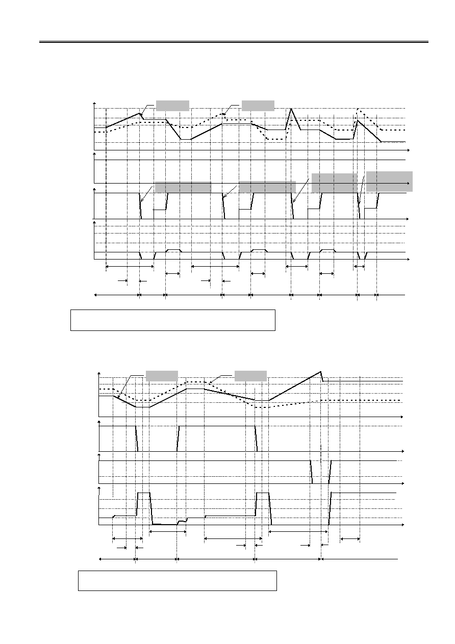
Operation Timing Charts
1. Overcharge detection
V2 auxiliary
over voltage detect
V2 Over voltage detect
V1 auxiliary
over voltage detect
V1 Over voltage detect
Vcuaux
Vcu
Vcd
Vdu
Vdd
Vss
Vcc
Vss
Vcc
Vss
EB-
Vcc
Viov2
Viov1
Vss
EB-
Battery
voltage
V1 battery
V2 battery
DO
terminal
CO
terminal
VM
terminal
Charger
connected
Load
connected
Mode
Delay
Delay
Note: Normal mode, Over charge mode, Over discharge mode, over current mode
The charger is assumed to charge with a constant current.
Figure
3
2. Overdischarge detection
Vcu
Vcd
Vdu
Vdd
Vss
Vcc
Vss
Vcc
Vss
EB-
Vcc
Viov2
Viov1
Vss
EB-
Delay
&
V1 battery
V2 battery
Battery
voltage
DO
terminal
CO
terminal
VM
terminal
Mode
Charger
connected
Load
connecte
d
Delay
Delay
Note: Normal mode, Over charge mode, Over discharge mode, over current mode
The charger is assumed to charge with a constant current.
Figure 4

Battery Protection IC (for a 2-serial-cell pack)
S-8232 Series
Rev. 4.1
_00
14
Seiko Instruments Inc.
3. Overcurrent detection
Vcu
Vcd
Vdu
Vdd
Vcc
Vss
Vcc
Vss
EB-
Delay =
t
IOV1
Delay =
t
IOV2
Vcc
Viov1
Vss
EB-
Viov2
<
t
IOV1
V1,V2 battery
Battery
voltage
DO
terminal
CO
terminal
VM
terminal
Mode
Charger
connected
Load
connected
Note: Normal mode, Over charge mode, Over discharge mode, over current mode
The charger is assumed to charge with a constant current.
Figure 5
Battery Protection IC (for a 2-serial-cell pack)
Rev. 4.1
_00
S-8232 Series
Seiko Instruments Inc.
15
Battery Protection IC Connection Example
EB
+
EB -
S-8232 series
R2 1 k
R1 1 k
R4 1 k
VSS
DO
SENS
ICT
R3
C2
C3
CO
VM
Delay time
setting
FET1
FET2
VC
VCC
C1
Battery 2
Battery 1
0.22
Ķ
F
0.22
Ķ
F
1 k
0.22
Ķ
F
R5
4.7 M
Figure 6
Table 8 Constant
Symbol Parts
Purpose
Recom-
mended
min. max.
Remarks
FET1
Nch MOSFET
Charge control
-----
-----
-----
-----
FET2
Nch MOSFET
Discharge control
-----
-----
-----
-----
R1
Chip resistor
ESD protection
1 k
300
1
k
C1
Chip capacitor
Filter
0.22
ĶF 0
ĶF 1
ĶF
R2
Chip resistor
ESD protection
1 k
300
1
k
C2
Chip capacitor
Filter
0.22
ĶF 0
ĶF 1
ĶF
R4
Chip resistor
ESD protection
1 k
=R1 min. =R1 max. 1) Same value as R1 and R2
C3
Chip capacitor
Delay time setting
0.22
ĶF 0
ĶF 1
ĶF
2) Attention should be paid to leak current of C3.
R3
Chip resistor
Protection for charger
reverse connection
1 k
300
5
k
3) Discharge can't be stopped at less than 300
when a charger is reverse-connected.
R5
Chip resistor
0 V battery charging
inhibition
(4.7 M
) (1
M
) (10M)
4) R5 should be added when the product has 0 V
battery charge inhibition. Lower resistance
increases current consumption.
1)
R4 =R1 is required. Overcharge detection voltage increases by R4. For example 10 k
(R4) increases overcharge
detection voltage by 20 mV.
2)
The overcharge detection delay time (t
CU
), the overdischarge detection delay time (t
CD
), and the over current detection
delay time (t
IOV
) change with the external capacitor C3. See the electrical characteristics.
3)
When the resistor R3 is set less than 300
and a charger is reverse-connected, current which exceeds the power
dissipation of the package will flow and the IC may break. But excessive R3 causes increase of overcurrent detection
voltage 1 (V
IOV1
). V
IOV1
changes to V
IOV1
=(R3+R
vsm
)/R
vsm
◊V
IOV1
. For example 50 k
resistor (R3) increases overcurrent
detection voltage 1 (V
IOV1
) from 0.100 V to 0.113 V.
4)
A 4.7 M
resistor is needed for R5 to inhibit 0 V battery charging. Current consumption increases when the R5
resistance increases. R5 should be connected when the product has 0 V battery charging inhibition.
Note:
The above connection diagram and constants do not guarantee proper operations. Evaluate your actual application and set
constants properly.
Battery Protection IC (for a 2-serial-cell pack)
S-8232 Series
Rev. 4.1
_00
16
Seiko Instruments Inc.
Precautions
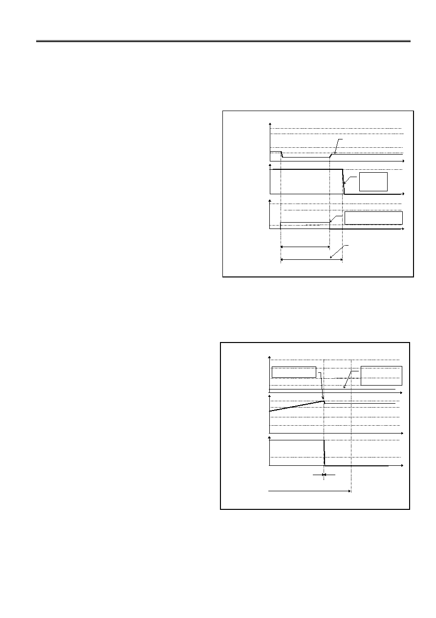
(1) After the overcurrent detection delay, if the battery voltages is equals the overdischarge detection voltage
(V
DD1,2
) or lower, the overdischarge detection delay time becomes shorter than 10ms (min.).
It occurs because capacitor C3 sets all of delay times. (Refer fig.7)
[ Cause ]
It occurs because capacitor C3 sets all of delay
times. When overcurrent detection is released
until t
IOV1
, the capacitor C3 is charged by S-
8232. If all battery voltage is lower than V
DD1,2
at
that time, charging goes on. So delay time is
shorter then typical.
[ Conclusion ]
This phenomenon occurs when all battery
voltage is nearly equal to the overdischarge
voltage (V
DD1,2
) after overcurrent detected. It
means that the battery capacity is small and
those must be charged in the future. Even if the
state changes to overdischarge condition, the
battery package capacity is same as typical.
(2) When one of the battery voltages is overdischarge detection voltage(V
DD1,2
) or lower and the other one
becomes higher than the overcharge detection voltage(V
CU1,2
), the IC detects the overcharge without the
overcharge detection delay time(t
CU
). (Refer fig.8)
[ Cause ]
It is same as the overdischarge detection under
the overcurrent condition. It occurs because
capacitor C3 sets all of delay times.
[ Conclusion ]
This phenomenon occurs when one battery
voltage is lower than overdischarge voltage
(V
DD1,2
) and batteries are charged by charger.
Under this situation voltage difference between
two batteries is unusual. Without delay time is
better than long delay time for battery pack
safety.(Refer fig.8)
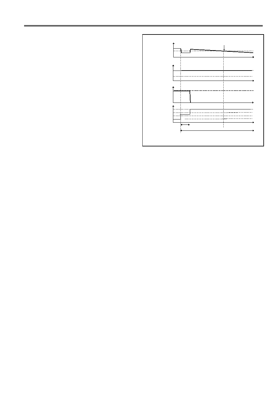
(3) After the overcurrent detection, the load was connected for a long time, even if one of the battery voltage
became lower than overdischarge detection voltage (V
DD1,2
), the IC can't detects the overdischarge as long as
the load is connected. Therefor the IC's current consumption at the one of the battery voltage is lower than the
overdischarge detection voltage is same as normal condition current consumption (I
OPE
) . (Refer fig.9)
Vcu
Vcd
Vdu
Vdd
Vcc
Vss
The over current
delay
Load
connect
Vcc
Viov2
Viov1
Vss
The over discharge
delay
The over current returns to
normal current.
the over
discharge
detection
The battery voltages is
equal to or less the over
discharge voltage.
The delay time becomes
shorter than usual.
Battery
voltage
DO
terminal
VM
terminal
Figure 7
Vcu
Vcd
Vdu
Vdd
Battery 1
voltage
Vcc
Vss
EB-
Charger connected
Over discharge
state
Over voltage detect
Delay time = 0
Vcu
Vcd
Vdu
Vdd
Battery 2
voltage
CO
terminal
Figure 8
Battery Protection IC (for a 2-serial-cell pack)
Rev. 4.1
_00
S-8232 Series
Seiko Instruments Inc.
17
[ Cause ]
The reason is as follows. If the overcurrent
detection and overdischarge detection occur at
same time, the overcurrent detection takes
precedence the overdischarge detection.
As long as the IC detects overcurrent, the IC
can't detect overdischarge.
[ Conclusion ]
If the load is taken off at least one time, the
overcurrent is released and the overdischarge
detection works.
Unless keeping the IC(S-8232) with load for a
long time, the reduction of battery voltage will be
neglected, because of the IC's(S-8232) current
consumption(typ. 7.5
ĶA) is small.
(4) Do not apply an electrostatic discharge to this IC that exceeds the performance ratings of the built-in electrostatic
protection circuit.
Vdd
0V
Vcc
Vss
The over current
delay
Load
connect
Vcc
Viov2
Viov1
Vss
EB-
The battery voltages is less than the over discharge voltage,
by self current consumption.
Battery
voltage
DO
terminal
VM
terminal
Iope
Ipdn
0A
Current
Consumption
As long as the load is connected, the IC's current consumption is same
as normal current consumption (Iope).
Figure 9
Battery Protection IC (for a 2-serial-cell pack)
S-8232 Series
Rev. 4.1
_00
18
Seiko Instruments Inc.
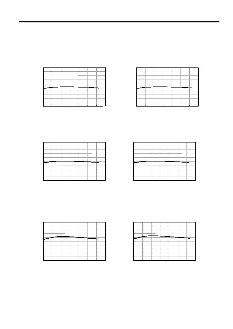
Characteristics(typical characteristics)
1. Detection voltage temperature characteristics
4.2
4.3
4.4
-40
-20
0
20
40
60
80
100
V
CU1
=4.30 [V]
Ta(įC)
V
CU1
(V
)
Overcharge detection voltage1 vs. temperature
4.2
4.3
4.4
-40
-20
0
20
40
60
80
100
V
CU2
=4.30 [V]
Ta(įC)
V
CU2
(V
)
Overcharge detection voltage2 vs. temperature
3.9
4
4.1
-40
-20
0
20
40
60
80
100
V
CD1
=4.00 [V]
Ta(įC)
V
CD1
(V
)
Overcharge release voltage1 vs. temperature
3.9
4
4.1
-40
-20
0
20
40
60
80
100
Ta(įC)
3.9
4
4.1
-40
-20
0
20
40
60
80
100
V
CD2
=4.00 [V]
Ta(įC)
V
CD2
(V
)
Overcharge release voltage2 vs. temperature
5.25
5.35
5.45
V
CUaux1
=5.375[V]
-40
-20
0
20
40
60
80
100
Ta(įC)
V
CUa
ux
1
(V
)
Auxiliary overcharge detection voltage1 vs. temperature
5.25
5.35
5.45
V
CUaux2
=5.375[V]
-40
-20
0
20
40
60
80
100
Ta(įC)
V
CUa
ux
2
(V
)
Auxiliary overcharge detection voltage2 vs. temperature

Battery Protection IC (for a 2-serial-cell pack)
Rev. 4.1
_00
S-8232 Series
Seiko Instruments Inc.
19
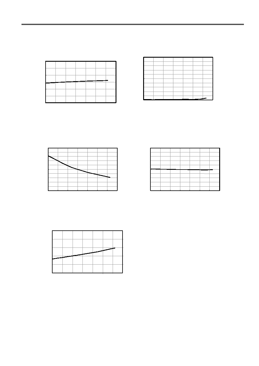
1.9
2
2.1
-40
-20
0
20
40
60
80
100
V
DD1
=2.00 [V]
Ta(įC)
V
DD1
(V
)
Overdischarge detection voltage1 vs. temperature
1.9
2
2.1
-40
-20
0
20
40
60
80
100
V
DD2
=2.00 [V]
Ta(įC)
V
DD2
(V
)
Overdischarge detection voltage2 vs. temperature
2.5
2.6
2.7
-40
-20
0
20
40
60
80
100
V
DU1
=2.60 [V]
Ta(įC)
V
DU1
(V
)
Overdischarge release voltage1 vs. temperature
2.5
2.6
2.7
-40
-20
0
20
40
60
80
100
V
DU2
=2.60 [V]
Ta(įC)
V
DU2
(V
)
Overdischarge release voltage1 vs. temperature
0.08
0.12
-40
-20
0
20
40
60
80
100
V
IOV1
=0.1 [V]
Ta(įC)
V
IOV1
(V
)
Overcurrent1 detection voltage vs. temperature
0.10
-1.30
-1.25
-1.20
-1.15
-1.10
-40
-20
0
20
40
60
80
100
V
IOV2
(V
)
Overcurrent1 detection voltage vs. temperature
V
IOV2
=1.20 [V] (V
CC
reference)
Ta(įC)
Battery Protection IC (for a 2-serial-cell pack)
S-8232 Series
Rev. 4.1
_00
20
Seiko Instruments Inc.
2.Current consumption temperature characteristics
0
5
10
15
-40 -20 0 20 40 60 80 100
V
CC
=7.2 [V]
Ta(įC)
I
OPE
(u
A
)
Current consumption vs. temperature in normal mode
0
50
100
-40
-20
0
20
40
60
80
100
V
CC
=3.0 [V]
Ta(įC)
I
PDN
(n
A
)
Current consumption vs. temperature in power-down mode
3. Delay time temperature characteristics
0.5
1
1.5
-40
-20
0
20
40
60
80
100
C3=0.22 [uF]
Ta(įC)
t
CU
(s)
Overcharge detection1 time vs. temperature
50
100
150
-40
-20
0
20
40
60
80
100
C3=0.22 [uF]
Ta(įC)
T
DD
(m
s
)
Overcharge detection1 time vs. temperature
7
8
9
10
11
12
-40 -20 0 20 40 60 80 100
C3=0.22 [uF]
Ta(įC
)
t
IOV1
(m
s
)
Overcurrent1 detection time vs. temperature
No.
TITLE
SCALE
UNIT
mm
Seiko Instruments Inc.
0.17Ī0.05
3.00
+0.3
-0.2
0.65
0.2Ī0.1
1
4
5
8
TSSOP8-A-PKG Dimensions
No. FT008-A-P-SD-1.1
FT008-A-P-SD-1.1
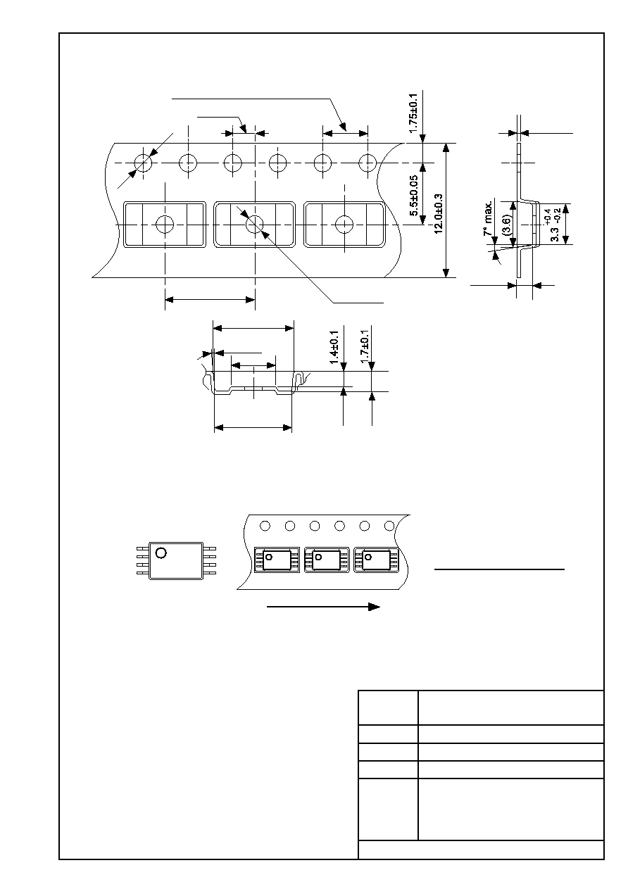
No.
TITLE
SCALE
UNIT
mm
Seiko Instruments Inc.
1.55Ī0.05
2.0Ī0.05
8.0Ī0.1
1.55
+0.1
-0
(6.9)
4.0
+0.4
-0.2
6.6
1.4Ī0.1
0.3Ī0.05
7į max.
1
4
5
8
4.0Ī0.1(50 pitches:200.0Ī0.3)
Feed direction
TSSOP8-A-Carrier Tape
No. FT008-A-C-SD-3.1
FT008-A-C-SD-3.1
No.
TITLE
SCALE
UNIT
mm
Seiko Instruments Inc.
13.4Ī1.0
17.5Ī1.0
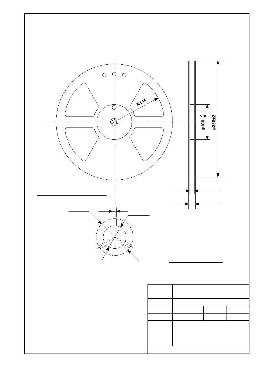
Ý13Ī0.5
2Ī0.5
Ý21Ī0.8
QTY.
3,000
Enlarged drawing in the central part
TSSOP8-A-Reel
No. FT008-A-R-SD-3.1
FT008-A-R-SD-3.1

∑
The information described herein is subject to change without notice.
∑
Seiko Instruments Inc. is not responsible for any problems caused by circuits or diagrams described herein
whose related industrial properties, patents, or other rights belong to third parties. The application circuit
examples explain typical applications of the products, and do not guarantee the success of any specific
mass-production design.
∑
When the products described herein are regulated products subject to the Wassenaar Arrangement or other
agreements, they may not be exported without authorization from the appropriate governmental authority.
∑
Use of the information described herein for other purposes and/or reproduction or copying without the
express permission of Seiko Instruments Inc. is strictly prohibited.
∑
The products described herein cannot be used as part of any device or equipment affecting the human
body, such as exercise equipment, medical equipment, security systems, gas equipment, or any apparatus
installed in airplanes and other vehicles, without prior written permission of Seiko Instruments Inc.
∑
Although Seiko Instruments Inc. exerts the greatest possible effort to ensure high quality and reliability, the
failure or malfunction of semiconductor products may occur. The user of these products should therefore
give thorough consideration to safety design, including redundancy, fire-prevention measures, and
malfunction prevention, to prevent any accidents, fires, or community damage that may ensue.