Rev.3.2
_10
BATTERY PROTECTION IC
FOR 3-SERIAL-CELL PACK
S-8233A Series
Seiko Instruments Inc.
1
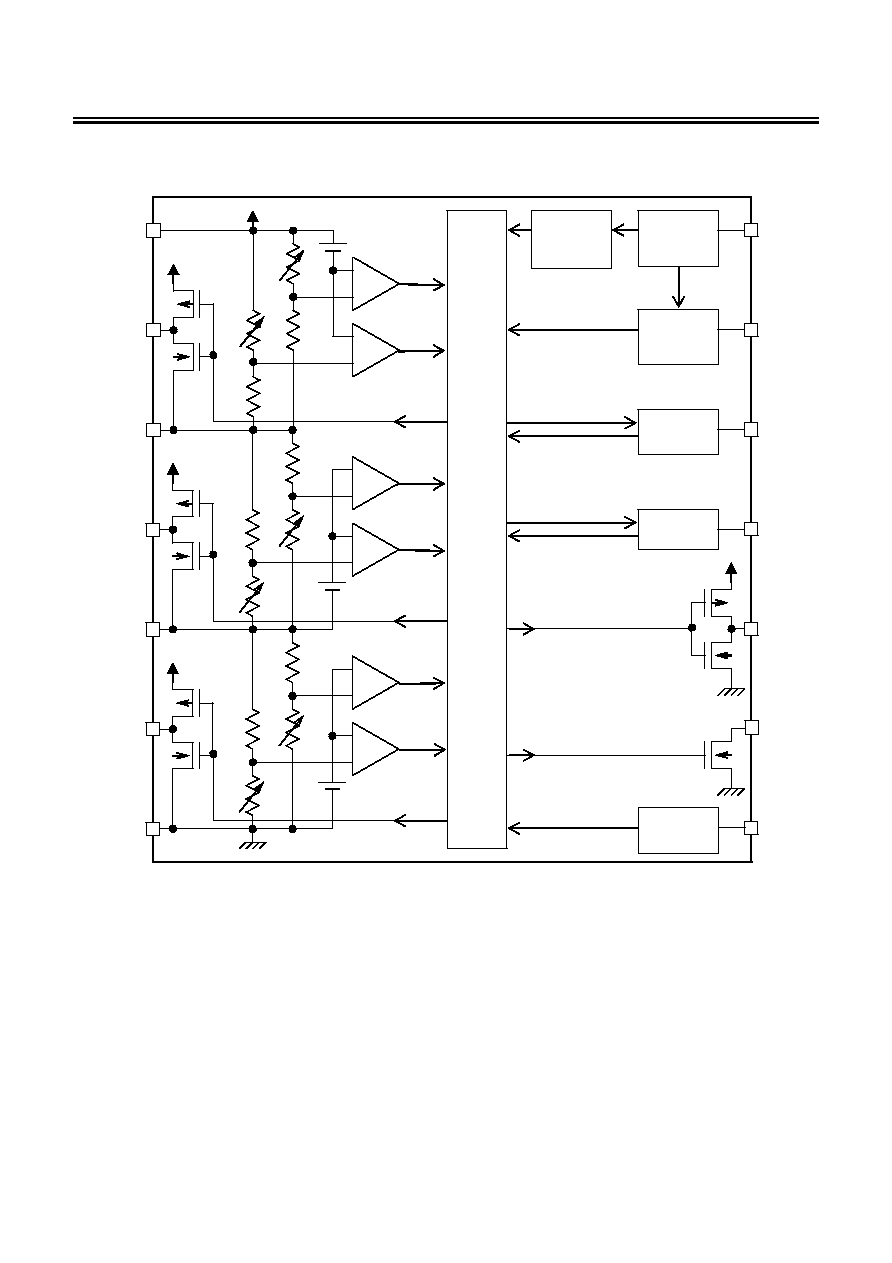
The S-8233A Series is a series of lithium-ion rechargeable battery
protection ICs incorporating high-accuracy voltage detection circuits and
delay circuits. It is suitable for a 3-serial-cell lithium-ion battery pack.
Features
(1)
Internal high-accuracy voltage detection circuit
Over charge detection voltage
4.10
± 0.05 V to 4.35 ± 0.05 V
50 mV- step
Over charge release voltage
3.85
± 0.10 V to 4.35 ± 0.10 V
50 mV- step
(The over charge release voltage can be selected within the range where a difference from over
charge detection voltage is 0 V to 0.3 V)
Over discharge detection voltage
2.00
± 0.08 V to 2.70± 0.08 V
100 mV- step
Over discharge release voltage
2.00
± 0.10 V to 3.70± 0.10 V
100 mV - step
(The over discharge release voltage can be selected within the range where a difference from over
discharge detection voltage is 0 V to 1.0 V)
Over current detection voltage 1
0.15
±0.015 V to 0.5 ±0.05 V
50 mV-step
(2)
High input-voltage device (absolute maximum rating: 26 V)
(3)
Wide operating voltage range:
2 V to 24 V
(4)
The delay time for every detection can be set via an external capacitor.
(5)
Three over current detection levels (protection for short-circuiting)
(6)
Internal charge/discharge prohibition circuit via the control terminal
(7)
The function for charging batteries from 0 V is available.
(8) Low
current
consumption
Operation 50
µA max. (+25 ∞C)
Power-down 0.1
µA max. (+25 ∞C)
Applications
Lithium-ion rechargeable battery packs
Packages
Drawing Code
Package Name
Package Tape Reel
14-Pin SOP
FE014-A
FE014-A
FE014-A
16-Pin TSSOP
FT016-A
FT016-A
FT016-A

BATTERY PROTECTION IC FOR 3-SERIAL-CELL PACK
Rev.3.2
_10
S-8233A Series
Seiko Instruments Inc.
3
Product Name Structure
1. Product name
S
-8233A x xx - TB
IC direction in tape specifications
*1
Package name (abbreviation)
FE: 14-Pin SOP
FT: 16-Pin TSSOP
Serial code
Assigned from A to Z in alphabetical order
*1. Refer to the taping specifications.
BATTERY PROTECTION IC FOR 3-SERIAL-CELL PACK
S-8233A Series
Rev.3.2
_10
Seiko Instruments Inc.
4
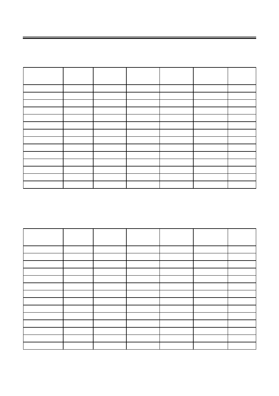
2. Product name list
14-Pin SOP
Table 1
Product name /
Parameter
Overcharge
detection voltage
V
CU
Overcharge
release voltage
V
CD
Overdischarge
detection voltage
V
DD
Overdischarge
release voltage
V
DU
Overcurrent
detection voltage1
V
IOV1
0 V battery
charge function
S-8233ACFE-TB
4.25±0.05 V
4.05±0.10 V
2.00±0.08 V
2.30±0.10 V
0.20±0.02 V
S-8233ADFE-TB 4.10±0.05
V 4.10
*1
2.00±0.08 V
2.30±0.10 V
0.20±0.02 V
S-8233AEFE-TB
4.25±0.05 V
4.10±0.10 V
2.30±0.08 V
2.70±0.10 V
0.15±0.015 V
S-8233AFFE-TB
4.35±0.05 V
4.05±0.10 V
2.40±0.08 V
2.70±0.10 V
0.50±0.05 V
Available
S-8233AGFE-TB
4.25±0.05 V
4.05±0.10 V
2.40±0.08 V
2.70±0.10 V
0.40±.0.04 V
Available
S-8233AIFE-TB
4.25±0.05 V
4.10±0.10 V
2.30±0.08 V
3.00±0.10 V
0.15±0.015 V
S-8233AJFE-TB
4.35±0.05 V
4.05±0.10 V
2.40±0.08 V
2.70±0.10 V
0.30±0.03 V
S-8233AKFE-TB
4.35±0.05 V
4.05±0.10 V
2.40±0.08 V
2.70±0.10 V
0.15±0.015 V
S-8233ALFE-TB
4.35±0.05 V
4.05±0.10 V
2.40±0.08 V
2.70±0.10 V
0.40±0.04 V
Available
S-8233AMFE-TB
4.35±0.05 V
4.05±0.10 V
2.40±0.08 V
2.70±0.10 V
0.30±0.03 V
Available
S-8233ANFE-TB
4.35±0.05 V
4.05±0.10 V
2.40±0.08 V
2.40±0.10 V
0.15±0.015 V
Available
S-8233AOFE-TB
4.35±0.05 V
4.05±0.10 V
2.40±0.08 V
2.70±0.10 V
0.15±0.015 V
Available
S-8233APFE-TB
4.25±0.05 V
4.05±0.10 V
2.70±0.08 V
3.00±0.10 V
0.30±0.03 V
Available
S-8233AQFE-TB 4.25±0.05
V 4.25
*1
2.70±0.08 V
3.00±0.10 V
0.30±0.03 V
Available
*1. Without over charge detection hysteresis.
Remark Please contact the SII marketing department for the products with the detection voltage value other
than those specified above.
16-Pin TSSOP
Table 2
Product name /
Parameter
Overcharge
detection voltage
V
Cu
Overcharge
release voltage
V
CD
Overdischarge
detection voltage
V
DD
Overdischarge
release voltage
V
DU
Overcurrent
detection voltage1
V
IOV1
0 V battery
charge function
S-8233ACFT-TB
4.25±0.05 V
4.05±0.10 V
2.00±0.08 V
2.30±0.10 V
0.20±0.02 V
S-8233ADFT-TB 4.10±0.05
V 4.10
*1
2.00±0.08 V
2.30±0.10 V
0.20±0.02 V
S-8233AEFT-TB
4.25±0.05 V
4.10±0.10 V
2.30±0.08 V
2.70±0.10 V
0.15±0.015 V
S-8233AFFT-TB
4.35±0.05 V
4.05±0.10 V
2.40±0.08 V
2.70±0.10 V
0.50±0.05 V
Available
S-8233AGFT-TB
4.25±0.05 V
4.05±0.10 V
2.40±0.08 V
2.70±0.10 V
0.40±.0.04 V
Available
S-8233AIFT-TB
4.25±0.05 V
4.10±0.10 V
2.30±0.08 V
3.00±0.10 V
0.15±0.015 V
S-8233AJFT-TB
4.35±0.05 V
4.05±0.10 V
2.40±0.08 V
2.70±0.10 V
0.30±0.03 V
S-8233AKFT-TB
4.35±0.05 V
4.05±0.10 V
2.40±0.08 V
2.70±0.10 V
0.15±0.015 V
S-8233ALFT-TB
4.35±0.05 V
4.05±0.10 V
2.40±0.08 V
2.70±0.10 V
0.40±0.04 V
Available
S-8233AMFT-TB
4.35±0.05 V
4.05±0.10 V
2.40±0.08 V
2.70±0.10 V
0.30±0.03 V
Available
S-8233ANFT-TB
4.35±0.05 V
4.05±0.10 V
2.40±0.08 V
2.40±0.10 V
0.15±0.015 V
Available
S-8233AOFT-TB
4.35±0.05 V
4.05±0.10 V
2.40±0.08 V
2.70±0.10 V
0.15±0.015 V
Available
S-8233APFT-TB
4.25±0.05 V
4.05±0.10 V
2.70±0.08 V
3.00±0.10 V
0.30±0.03 V
Available
S-8233ARFT-TB
4.35±0.05 V
4.05±0.10 V
2.00±0.08 V
2.70±0.10 V
0.30±0.03 V
Available
*1. Without over charge detection hysteresis.
Remark Please contact the SII marketing department for the products with the detection voltage value other
than those specified above.
BATTERY PROTECTION IC FOR 3-SERIAL-CELL PACK
Rev.3.2
_10
S-8233A Series
Seiko Instruments Inc.
5
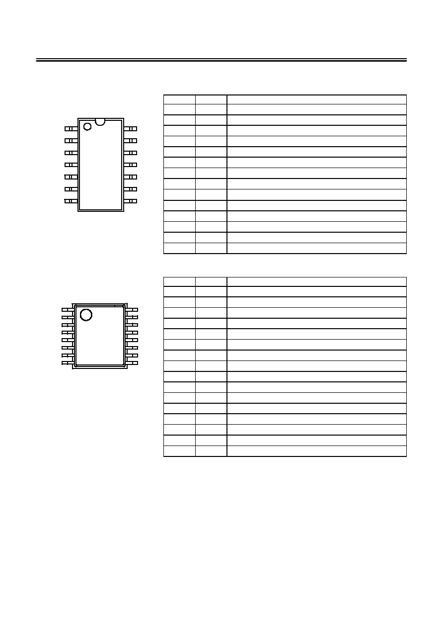
Pin Assignment
Table
3
Pin No. Symbol
Pin description
1 DOP
Connects FET gate for discharge control (CMOS output)
2 COP
Connects FET gate for charge control (Nch open-drain output)
3 VMP
Detects voltage between VCC to VMP(Over current detection pin)
4 COVT
Connects capacitor for over current detection1delay circuit
5 CDT
Connects capacitor for over discharge detection delay circuit
6 CCT
Connects capacitor for over charge detection delay circuit
7 VSS
Negative power input, and connects negative voltage for battery 3
8 CTL
Charge/discharge control signal input
9 CD3
Battery 3 conditioning signal output
10 VC2
Connects battery 2 negative voltage and battery 3 positive voltage
11 CD2
Battery 2 conditioning signal output
12 VC1
Connects battery 1 negative voltage and battery 2 positive voltage
13 CD1
Battery 1 conditioning signal output
VSS
VMP
VCC
CTL
14
13
12
11
10
9
8
7
6
5
4
3
2
1
DOP
COP
CCT
COVT
CDT
VC1
VC2
CD1
CD3
CD2
14-Pin SOP
Top view
Figure 2
14 VCC
Positive power input and connects battery 1 positive voltage
Table 4
Pin No. Symbol
Pin description
1 DOP
Connects FET gate for discharge control (CMOS output)
2 NC
No connection
*1
3 COP
Connects FET gate for charge control (Nch open-drain output)
4 VMP
Detects voltage between VCC to VMP(Over current detection pin)
5 COVT
Connects capacitor for over current detection1 delay circuit
6 CDT
Connects capacitor for over discharge detection delay circuit
7 CCT
Connects capacitor for over charge detection delay circuit
8 VSS
Negative power input, and connects negative voltage for battery 3
9 CTL
Charge/discharge control signal input
10 CD3
Battery 3 conditioning signal output
11 VC2
Connects battery 2 negative voltage and battery 3 positive voltage
12 CD2
Battery 2 conditioning signal output
13 VC1
Connects battery 1 negative voltage and battery 2 positive voltage
14
CD1 Battery 1 conditioning signal output
15 NC
No connection
*1
VSS
VMP
VCC
CTL
14
13
12
11
10
9
7
6
5
4
3
2
1
DOP
COP
CCT
COVT
CDT
VC1
VC2
CD1
CD3
CD2
16-Pin TSSOP
Top view
8
15
16
NC
NC
Figure
3
16 VCC
Positive power input and connects battery 1 positive voltage
*1. The NC pin is electrically open. The NC pin can be connected to
VCC or VSS.