Document Outline
- S-8233A Series
- Cover
- Features
- Applications
- Selection Guide
- Block Diagram
- Pin Assignment
- Pin Description
- Absolute Maximum Ratings
- Electrical Characteristics
- Measurement Circuits
- Description
- Operation Timing Charts
- Battery Protection IC Connection Example
- Precautions
- Characteristics (typical characteristics)
- Package Drawing

Seiko Instruments Inc.
1
Rev.3.1
_
00
BATTERY PROTECTION IC (FOR A 3-SERIAL-CELL PACK)
S-8233A SERIES
The 8233A is a series of lithium-ion rechargeable battery protection ICs
incorporating high-accuracy voltage detection circuits and delay
circuits. It is suitable for a 3-serial-cell lithium-ion battery pack.
Features
(1) Internal high-accuracy voltage detection circuit
Over charge detection voltage
4.10
± 0.05 V to 4.35 ± 0.05 V
0.05 V- step
Over charge release voltage
3.85
± 0.10 V to 4.35 ± 0.10 V
0.05 V- step
(The over charge release voltage can be selected within the range where a difference from over
charge detection voltage is 0 to 0.3 V)
Over discharge detection voltage
2.00
± 0.08 V to 2.70± 0.08 V
0.10 V- step
Over discharge release voltage
2.00
± 0.10 V to3.70± 0.10 V
0.10 V - step
(The over discharge release voltage can be selected within the range where a difference from
over discharge detection voltage is 0 to 1.0V)
Over current detection voltage 1
0.15 V
±10% to 0.50 V±10%
0.05 V-step
(2)
High input-voltage device (absolute maximum rating: 26 V)
(3)
Wide operating voltage range:
2 V to 24 V
(4)
The delay time for every detection can be set via an external capacitor.
(5)
Three over current detection levels (protection for short-circuiting)
(6)
Internal charge/discharge prohibition circuit via the control terminal
(7)
The function for charging batteries from 0 V is available.
(8)
Low current consumption
Operation 50
µA max (+25 ∞C)
Power-down 0.1
µA max (+25 ∞C)
(9)
14-pin SOP package
Applications
Lithium-ion rechargeable battery packs
Battery Protection IC(for a 3-serial-cell pack)
S-8233A Series
Rev.3.1_
00
Seiko Instruments Inc.
2
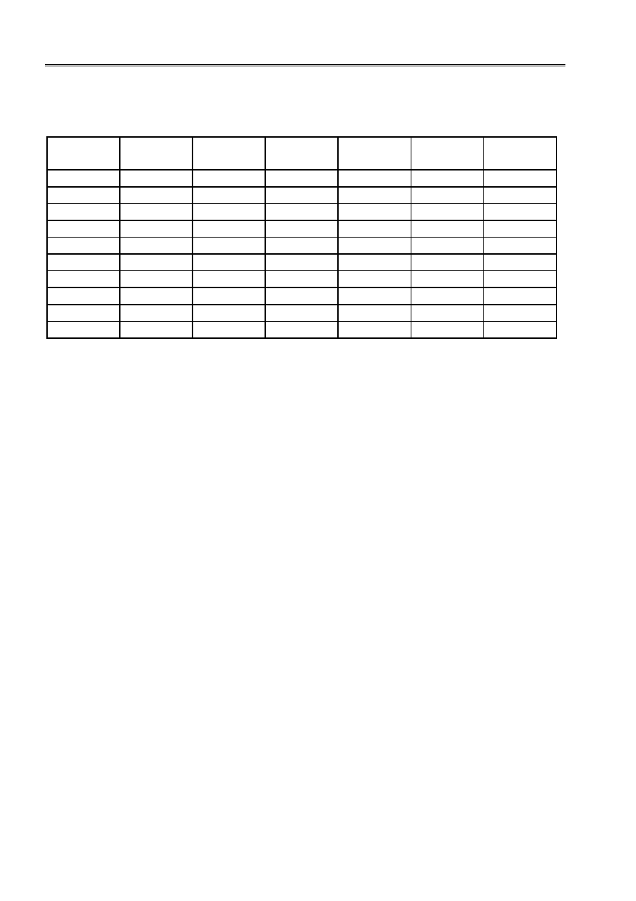
Selection Guide
Table1
Model/Item Over
charge
detection voltage
Over charge
release voltage
Over discharge
detection voltage
Over discharge
release voltage
Over current
detection voltage1
0V battery
charging function
S-8233ACFE/FT
4.25±0.05V 4.05±0.10V 2.00±0.08V 2.30±0.10V 0.20V±10%
-
S-8233ADFE/FT 4.10±0.05V
2.00±0.08V 2.30±0.10V 0.20V±10%
-
S-8233AEFE/FT
4.25±0.05V 4.10±0.10V 2.30±0.08V 2.70±0.10V 0.15V±10%
-
S-8233AFFE/FT
4.35±0.05V 4.05±0.10V 2.40±0.08V 2.70±0.10V 0.50V±10%
Available
S-8233AGFE/FT
4.25±0.05V 4.05±0.10V 2.40±0.08V 2.70±0.10V 0.40V±10%
Available
S-8233AIFE/FT
4.25±0.05V 4.10±0.10V 2.30±0.08V 3.00±0.10V 0.15V±10%
-
S-8233AJFE/FT
4.35±0.05V 4.05±0.10V 2.40±0.08V 2.70±0.10V 0.30V±10%
-
S-8233AKFE/FT
4.35±0.05V 4.05±0.10V 2.40±0.08V 2.70±0.10V 0.15V±10%
-
S-8233ALFE/FT
4.35±0.05V 4.05±0.10V 2.40±0.08V 2.70±0.10V 0.40V±10%
Available
S-8233AMFE/FT
4.35±0.05V 4.05±0.10V 2.40±0.08V 2.70±0.10V 0.30V±10%
Available
Without over charge detection hysteresis.
Last 2 digits shows package type. FE
14pin SOP, FT16pin TSSOP
Change in the detection voltage is available in products other than the above listed ones. Contact the
SII Semiconductor Products Sales Department.
Battery Protection IC(for a 3-serial-cell pack)
Rev.3.1_
00
S-8233A Series
Seiko Instruments Inc.
3
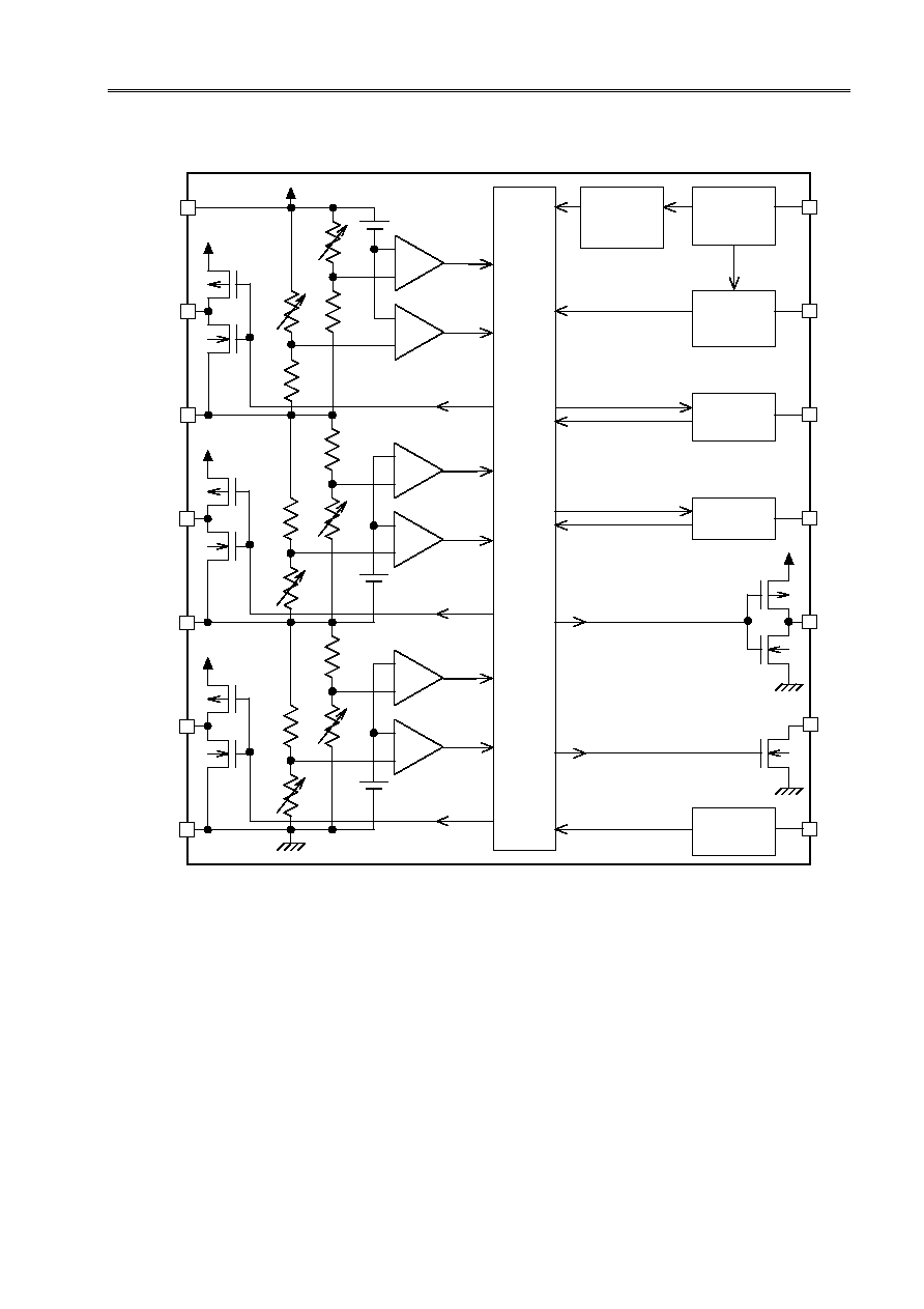
Block Diagram
Battery 1
Over charge
Battery 3
Over discharge
Battery 3
Over charge
Battery 2
Over charge
Battery 2
Over discharge
Over charge
delay circuit
Battery 1
Over discharge
Battery 3
Over charge
Battery 2
Over charge
Battery 1
Over charge
Reference
voltage 3
Reference
voltage 2
Reference
voltage 1
Control
Logic
Over current
detection
circuit
Over discharge
delay circuit
Over current,P
delay circuit
Over current
2,3 delay circuit
-
+
-
+
-
+
-
+
-
+
-
+
DOP
VMP
COVT
CDT
CCT
COP
CTL
VSS
CD3
VC2
CD2
CD1
VC1
VCC
Floating
detection circuit
Figure 1
The delay time for over current detection 2 and 3 is fixed by an internal IC circuit. The delay time
cannot be changed via an external capacitor.
Battery Protection IC(for a 3-serial-cell pack)
S-8233A Series
Rev.3.1_
00
Seiko Instruments Inc.
4
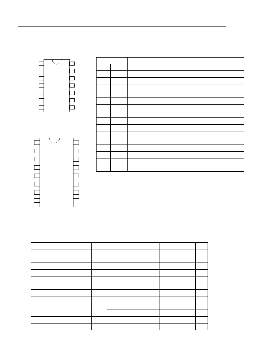
Pin Assignment
Top View
VSS
VMP
VCC
CTL
14
13
12
11
10
9
8
7
6
5
4
3
2
1
DOP
COP
CCT
COVT
CDT
VC1
VC2
CD1
CD3
CD2
SOP-14
Figure 2(a)
Top View
VSS
VMP
VCC
CTL
14
13
12
11
10
9
7
6
5
4
3
2
1
DOP
COP
CCT
COVT
CDT
VC1
VC2
CD1
CD3
CD2
8
15
16
NC
NC
T
TSSOP-16
Figure 2(b)
Pin Description
Table 2
No. Name
Description
SOP14 TSSOP16
1
1
DOP Connects FET gate for discharge control (CMOS output)
2
3
COP Connects FET gate for charge control (Nch open-drain output)
3
4
VMP Detects voltage between VCC to VMP(Over current detection pin)
4
5
COVT Connects capacitor for over current detection1delay circuit
5
6
CDT Connects capacitor for over discharge detection delay circuit
6
7
CCT Connects capacitor for over charge detection delay circuit
7
8
VSS Negative power input, and connects negative voltage for battery 3
8
9
CTL Charge/discharge control signal input
9
10
CD3 Battery 3 conditioning signal output
10
11
VC2 Connects battery 2 negative voltage and battery 3 positive voltage
11
12
CD2 Battery 2 conditioning signal output
12
13
VC1 Connects battery 1 negative voltage and battery 2 positive voltage
13
14
CD1 Battery 1 conditioning signal output
14
16
VCC Positive power input and connects battery 1 positive voltage
--- 2,15 NC
Non
connect
Absolute Maximum Ratings
Table 3
Ta = 25
∞C
Item Sym.
Applied
Pins Rating
Unit
Input voltage between VCC and VSS
VDS
VSS-0.3 to 26
V
Input terminal voltage
VIN
VC1,VC2,CTL,CCT,CDT,COVT VSS-0.3 to VCC+0.3
V
VMP Input terminal voltage
VVMP
VMP
VSS-0.3 to 26
V
CD1 output terminal voltage
VCD1
CD1
VC1-0.3 to VCC+0.3
V
CD2 output terminal voltage
VCD2
CD2
VC2-0.3 to VCC+0.3
V
CD3 output terminal voltage
VCD3
CD3
VSS-0.3 to VCC+0.3
V
DOP output terminal voltage
VDOP
DOP
VSS-0.3 to VCC+0.3
V
COP output terminal voltage
VCOP
COP
VSS-0.3 to 26
V
Power dissipation
PD
SOP-14PKG
400
mW
TSSOP-16PKG 300
mW
Operating temperature range
Topr
-20 to +70
∞C
Storage temperature range
Tstg
-40 to +125
∞C

Battery Protection IC(for a 3-serial-cell pack)
Rev.3.1_
00
S-8233A Series
Seiko Instruments Inc.
5
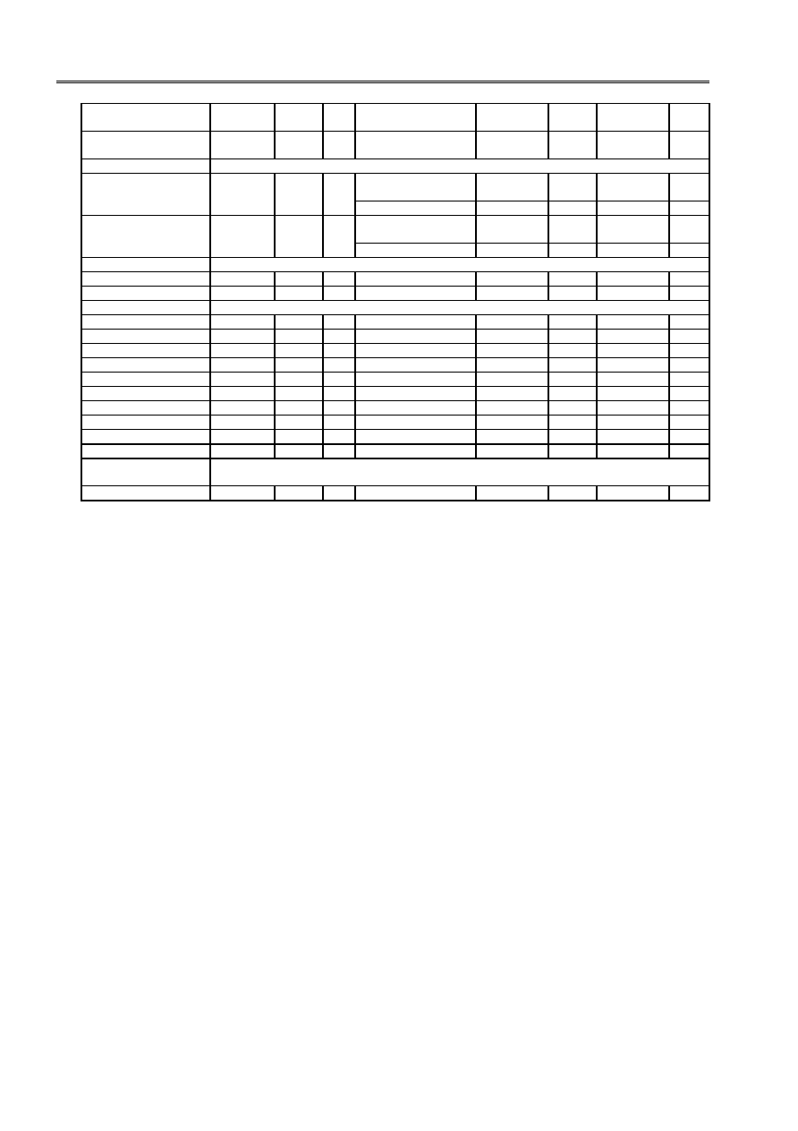
Electrical Characteristics
Table 4
Ta = 25∞C
Item Symbol
condition
Test
circuit
Notice Min.
Typ.
Max.
Unit
Detection voltage
Over charge detection
voltage1
VCU1
1
1 4.10 to 4.35 Adjustment VCU1-0.05
VCU1
VCU1+0.05
V
Over charge release
voltage1
VCD1
1
1 3.85 to 4.35 Adjustment VCD1-0.10
VCD1
VCD1+0.10
V
Over discharge detection
voltage1
VDD1
1
1 2.00 to 2.70 Adjustment VDD1-0.08
VDD1
VDD1+0.08
V
Over discharge release
voltage1
VDU1
1
1 2.00 to 3.70 Adjustment VDU1-0.10
VDU1
VDU1+0.10
V
Over charge detection
voltage 2
VCU 2
2
1 4.10 to 4.35 Adjustment VCU2-0.05
VCU2
VCU2+0.05
V
Over charge release
voltage 2
VCD 2
2
1 3.85 to 4.35 Adjustment VCD2-0.10
VCD2
VCD2+0.10
V
Over discharge detection
voltage 2
VDD 2
2
1 2.00 to 2.70 Adjustment VDD2-0.08
VDD2
VDD2+0.08
V
Over discharge release
voltage 2
VDU 2
2
1 2.00 to 3.70 Adjustment VDU2-0.10
VDU2
VDU2+0.10
V
Over charge detection
voltage3
VCU3
3
1 4.10 to 4.35 Adjustment VCU3-0.05
VCU3
VCU3+0.05
V
Over charge release
voltage3
VCD3
3
1 3.85 to 4.35 Adjustment VCD3-0.10
VCD3
VCD3+0.10
V
Over discharge detection
voltage3
VDD3
3
1 2.00 to 2.70 Adjustment VDD3-0.08
VDD3
VDD3+0.08
V
Over discharge release
voltage3
VDU3
3
1 2.00 to 3.70 Adjustment VDU3-0.10
VDU3
VDU3+0.10
V
Over current detection
voltage1
VIOV1 4
2
(*4)0.15 to 0.50V
Adjustment
VIOV1
◊0.9 VIOV1 VIOV1◊1.1 V
Over current detection
voltage 2
VIOV2 4
2
VCC
Reference 0.54 0.6 0.66 V
Over current detection
voltage3
VIOV3 4
2
VSS
Reference 1.0 2.0 3.0 V
Voltage temperature
factor 1
TCOE1
(*1)Ta=-20 to 70∞C
-1.0 0 1.0
mV/∞C
Voltage temperature
factor 2
TCOE2
(*2)Ta=-20 to 70∞C
-0.5 0 0.5
mV/∞C
Delay time
Over charge detection
delay time1
TCU1 9
6
CCCT=0.47
µF
0.5 1.0 1.5 S
Over charge detection
delay time 2
TCU2 10
6
CCCT=0.47
µF
0.5 1.0 1.5 S
Over charge detection
delay time3
TCU3 11
6
CCCT=0.47
µF
0.5 1.0 1.5 S
Over discharge detection
delay time1
TDD1 9
6
CCDT=0.1
µF
20 40 60
mS
Over discharge detection
delay time 2
TDD2 10
6
CCDT=0.1
µF
20 40 60
mS
Over discharge detection
delay time3
TDD3 11
6
CCDT=0.1
µF
20 40 60
mS
Over current detection
delay time1
TIOV1 1
2
7
CCOVT=0.1
µF
10 20 30
mS
Over current detection
delay time 2
TIOV2 1
2
7
2 4 8
mS
Over current detection
delay time3
TIOV3 1
2
7
FET gate capacitor
=2000pF
100 300 550
µS
Operating voltage
Operating voltage
between VCC and VSS
VDSOP
(*3) 2.0
-
24
V
Current consumption
Current consumption
(during normal operation)
IOPE
5
3
V1=V2=V3=3.5V - 20 50
µA
Current consumption for
cell 2
ICELL2
5
3
V1=V2=V3=3.5V -300 0 300 nA
Battery Protection IC(for a 3-serial-cell pack)
S-8233A Series
Rev.3.1_
00
Seiko Instruments Inc.
6
Current consumption for
cell 3
ICELL3
5
3
V1=V2=V3=3.5V -300 0 300 nA
Current consumption at
power down
IPDN
5
3
V1=V2=V3=1.5V - - 0.1
µA
Internal resistance
Resistance between
VCC and VMP
Rvcm 6
3
V1=V2=V3=3.5V 0.40 0.90 1.40 M
(*5)
0.20 0.50 0.80 M
Resistance between
VSS and VMP
Rvsm 6
3
V1=V2=V3=3.5V 0.40 0.90 1.40 M
(*5)
0.20 0.50 0.80 M
Input voltage
CTL"H" Input voltage
VCTL(H)
VCC
◊0.8 -
-
V
CTL"L" Input voltage
VCTL(L)
- -
VCC
◊0.2 V
Output voltage
DOP"H" voltage
VDO(H)
7
4
Iout=10uA
VCC-0.5
-
-
V
DOP"L" voltage
VDO(L)
7
4
Iout=10uA
-
-
VSS+0.1
V
COP"L" voltage
VCO(L)
8
5
Iout=10uA
-
-
VSS+0.1
V
COP OFF LEAK current
ICOL
14
9 V1=V2=V3=4.5V
-
-
100 nA
CD1"H" voltage
VCD1(H)
13
8
Iout=0.1uA
VCC-0.5
-
-
V
CD1"L" voltage
VCD1(L)
13
8
Iout=10uA
-
-
VC1+0.1
V
CD 2"H" voltage
VCD2(H)
13
8
Iout=0.1uA
VCC-0.5
-
-
V
CD 2"L" voltage
VCD2(L)
13
8
Iout=10uA
-
-
VC2+0.1
V
CD3"H" voltage
VCD3(H)
13
8
Iout=0.1uA
VCC-0.5
-
-
V
CD3"L" voltage
VCD3(L)
13
8
Iout=10uA
-
-
VSS+0.1
V
0V battery charging
function
0V charging start voltage V0CHAR
15
10 (*5)
- - 1.4
V
(*1) Voltage temperature factor 1 indicates over charge detection voltage, over charge release voltage,
over discharge detection voltage, and over discharge release voltage.
(*2) Voltage temperature factor 2 indicates over current detection voltage.
(*3) The DOP and COP logic must be established for the operating voltage.
(*4) If over current detection voltage 1 is 0.50 V, both over current detection voltages 1 and 2 are 0.54
to 0.55 V, but VIOV2 > VIOV1.
(*5) This spec applies for only 0 V battery charging function available type.

Battery Protection IC(for a 3-serial-cell pack)
Rev.3.1_
00
S-8233A Series
Seiko Instruments Inc.
7
Measurement Circuits
(1) Measurement 1 Measurement circuit 1
Set V1, V2, and V3 to 3.5 V under normal condition. Increase V1 from 3.5 V gradually. The V1 voltage
when COP = 'H' is over charge detection voltage 1 (VCU1). Decrease V1 gradually. The V1 voltage
when COP = 'L' is over charge release voltage 1 (VCD1). Further decrease V1. The V1 voltage when
DOP = 'H' is over discharge voltage 1 (VDD1). Increase V1 gradually. The V1 voltage when DOP = 'L'
is over discharge release voltage 1 (VDU1).
(2) Measurement 2 Measurement circuit 1
Set V1, V2, and V3 to 3.5 V under normal condition. Increase V2 from 3.5 V gradually. The V2 voltage
when COP = 'H' is over charge detection voltage 2 (VCU2). Decrease V2 gradually. The V2 voltage
when COP = 'L' is over charge release voltage 2 (VCD2). Further decrease V2. The V2 voltage when
DOP = 'H' is over discharge voltage 2 (VDD2). Increase V2 gradually. The V2 voltage when DOP = 'L'
is over discharge release voltage 2 (VDU2).
(3) Measurement 3 Measurement circuit 1
Set V1, V2, and V3 to 3.5 V under normal condition. Increase V3 from 3.5 V gradually. The V3 voltage
when COP = 'H' is over charge detection voltage 3 (VCU3). Decrease V3 gradually. The V3 voltage
when COP = 'L' is over charge release voltage 3 (VCD3). Further decrease V3. The V3 voltage when
DOP = 'H' is over discharge voltage 3 (VDD3). Increase V3 gradually. The V3 voltage when DOP = 'L'
is over discharge release voltage 3 (VDU3).
Note: The voltage change rate is 150 V/sec or less under measuring conditions 1 to 3.
(4) Measurement 4 Measurement circuit 2
Set V1, V2, V3 to 3.5 V and V4 to 0 V under normal condition. Increase V4 from 0 V gradually. The V4
voltage when DOP = 'H' and COP = 'H', is over current detection voltage 1 (VIOV1).
Set V1, V2, and V3 to 3.5 V and V4 to 0 V under normal condition. Fix the COVT terminal at VSS,
increase V4 from 0 V gradually. The V4 voltage when DOP = 'H' and COP = 'H' is over current
detection voltage 2 (VI0V2).
Set V1, V2, and V3 to 3.5 V and V4 to 0 V under normal condition. Fix the COVT terminal at VSS,
increase V4 gradually from 0 V at 400
µs to 2 ms. The V4 voltage when DOP = 'H' and COP = 'H' is
over current detection voltage 3 (VI0V3).
(5) Measurement 5 Measurement circuit 3
Set S1 to ON, V1, V2, and V3 to 3.5 V, and V4 to 0 V under normal condition and measure current
consumption. I1 is the normal condition current consumption (IOPE), I2, the cell 2 current consumption
(ICELL2), and I3, the cell 3 current consumption (ICELL3).
Set S1 to ON, V1, V2, and V3 to 1.5 V, and V4 to 4.5 V under over discharge condition. Current
consumption I1 is power-down current consumption (IPDN).
(6) Measurement 6 Measurement circuit 3
Set S1 to ON, V1, V2, and V3 to 3.5 V, and V4 to 10.5 V under normal condition. V4/I4 is the internal
resistance between VCC and VMP (RVCM).
Set S1 to ON, V1, V2, and V3 to 1.5 V, and V4 to 4.1 V under over discharge condition. (4.5-V4)/I4 is
the internal resistance between VSS and VMP (RVSM).

Battery Protection IC(for a 3-serial-cell pack)
S-8233A Series
Rev.3.1_
00
Seiko Instruments Inc.
8
(7) Measurement 7 Measurement circuit 4
Set S1 to ON, S2 to OFF, V1, V2, and V3 to 3.5 V, and V4 to 0 V under normal condition. Increase V5
from 0 V gradually. The V5 voltage when I1 = 10
µA is DOP'L' voltage (VD0 (L)).
Set S1 to OFF, S2 to ON, V1, V2, V3 to 3.5 V, and V4 to VIOV2+0.1 V under over current condition.
Increase V6 from 0 V gradually. The V6 voltage when I2 = 10
µA is the DOP'H' voltage (VDO (H)).
(8) Measurement 8 Measurement circuit 5
Set V1, V2, V3 to 3.5 V and V4 to 0 V under normal condition. Increase V5 from 0 V gradually. The V5
voltage when I1 = 10
µA is the COP'L' voltage (VC0 (L)).
(9) Measurement 9 Measurement circuit 6
Set V1, V2, V3 to 3.5 V under normal condition. Increase V1 from 3.5 V to 4.5 V immediately (within 10
µs). The time after V1 becomes 4.5 V until COP goes 'H' is the over charge detection delay time 1
(TCU1).
Set V1, V2, V3 to 3.5 V under normal condition. Decrease V1 from 3.5 V to 1.9 V immediately (within
10
µs). The time after V1 becomes 1.9 V until DOP goes 'H' is the over discharge detection delay time
1 (TDD1).
(10) Measurement 10 Measurement circuit 6
Set V1, V2, V3 to 3.5 V under normal condition. Increase V2 from 3.5 V to 4.5 V immediately (within 10
µs). The time after V2 becomes 4.5 V until COP goes 'H' is the over charge detection delay time 2
(TCU2).
Set V1, V2, V3 to 3.5 V under normal condition. Decrease V2 from 3.5 V to 1.9 V immediately (within
10
µs). The time after V2 becomes 1.9 V until DOP goes 'H' is the over discharge detection delay time
2 (TDD2).
(11) Measurement 11 Measurement circuit 6
Set V1, V2, V3 to 3.5 V under normal condition. Increase V3 from 3.5 V to 4.5 V immediately (within 10
µs). The time after V3 becomes 4.5 V until COP goes 'H' is the over charge detection delay time 3
(TCU3).
Set V1, V2, V3 to 3.5 V under normal condition. Decrease V3 from 3.5 V to 1.9 V immediately (within
10
µs). The time after V3 becomes 1.9 V until DOP goes 'H' is the over discharge detection delay time
3 (TDD3).
(12) Measurement 12 Measurement circuit 7
Set V1, V2, V3 to 3.5 V and S1 to OFF under normal condition. Increase V4 from 0 V to 0.55 V
immediately (within 10
µs). The time after V4 becomes 0.55 V until DOP goes 'H' is the over current
detection delay time 1 (TI0V1).
Set V1, V2, V3 to 3.5 V and S1 to OFF under normal condition. Increase V4 from 0 V to 0.75 V
immediately (within 10
µs). The time after V4 becomes 0.75 V until DOP goes 'H' is the over current
detection delay time 2 (TIOV2)
Set S1 to ON to inhibit over discharge detection. Set V1, V2, V3 to 4.0 V and increase V4 from 0 V to
6.0 V immediately (within 1
µs) and decrease V1, V2, and V3 to 2.0 V at a time. The time after V4
becomes 6.0 V until DOP goes 'H' is the over current detection delay time 3 (TIOV3).

Battery Protection IC(for a 3-serial-cell pack)
Rev.3.1_
00
S-8233A Series
Seiko Instruments Inc.
9
(13) Measurement 13 Measurement circuit 8
Set S4 to ON, S1, S2, S3, S5, and S6 to OFF, V1, V2, V3 to 3.5 V and V4, V6, and V7 to 0 V under
normal condition. Increase V5 from 0 V gradually. The V5 voltage when I2 = 10
µA is the CD1'L'
voltage (CD1(L))
Set S5 to ON, S1, S2, S3, S4, and S6 to OFF, V1, V2, and V3 to 3.5 V and V4, V5, and V7 to 0 V under
normal condition. Increase V6 from 0 V gradually. The V6 voltage when I3 = 10
µA is the CD2'L'
voltage (VCD2(L)).
Set S6 to ON, S1, S2, S3, S4, and S5 to OFF, V1, V2, and V3 to 3.5 V and V4, V5, and V6 to 0 V under
normal condition. Increase V7 from 0 V gradually. The V7 voltage when I4 = 10
µA is the CD3'L'
voltage (VCD3(L)).
Set S1 to ON, S2, S3, S4, S5, and S6 to OFF, V1 to 4.5 V, V2 and V3 to 3.5 V and V5, V6, and V7 to 0
V under over charge condition. Increase V4 from 0 V gradually. The V4 voltage when I1 = 0.1
µA is the
CD1'H' voltage (VCD1(H)).
Set S2 to ON, S1, S3, S4, S5, and S6 to OFF, V2 to 4.5 V, V1 and V3 to 3.5 V and V5, V6, and V7 to 0
V under over charge condition. Increase V4 from 0 V gradually. The V4 voltage when I1 = 0.1
µA is the
CD2'H' voltage (VCD2(H)).
Set S3 to ON, S1, S2, S4, S5, and S6 to OFF, V3 to 4.5 V, V1 and V2 to 3.5 V and V5, V6, and V7 to 0
V under over charge condition. Increase V4 from 0 V gradually. The V4 voltage when I1 = 0.1
µA is the
CD3'H' voltage (VCD3(H)).
(14) Measurement 14 Measurement circuit 9
Set V1, V2, and V3 to 4.5 V under over charge condition. The current I1 flowing to COP terminal is
COP OFF LEAK current (ICOL).
(15) Measurement 15 Measurement circuit 10
Set V1, V2, and V3 to 0 V, and V8 to 2 V, and decrease V8 gradually. The V8 voltage when COP = 'H'
(VSS + 0.1 V or higher) is the 0V charge start voltage (V0CHAR).
Note: The voltage change rate is 150 V/sec or less under the measuring condition.
Battery Protection IC(for a 3-serial-cell pack)
S-8233A Series
Rev.3.1_
00
Seiko Instruments Inc.
10
VSS
DOP
CTL
VC2
COP
VMP
VC1
CCT
COVT
CDT
VCC
CD3
CD2
CD1
V3
V2
V1
1M
Measurement circuit 1
VSS
DOP
CTL
VC2
COP
VMP
VC1
CCT
COVT
CDT
VCC
CD3
CD2
CD1
V3
V2
V1
V4
1M
Measurement circuit 2
VSS
DOP
CTL
VC2
COP
VMP
VC1
CCT
COVT
CDT
VCC
CD3
CD2
CD1
V3
V2
I2
I3
S1
I1
I4
V1
V4
Measurement circuit 3
VSS
DOP
CTL
VC2
COP
VMP
VC1
CCT
COVT
CDT
VCC
CD3
CD2
CD1
V3
V2
V1
V5
S1
I1
S2
I2
V6
V4
Measurement circuit 4
VSS
DOP
CTL
VC2
COP
VMP
VC1
CCT
COVT
CDT
VCC
CD3
CD2
CD1
V3
V2
V5
I1
V1
V4
Measurement circuit 5
VSS
DOP
CTL
VC2
COP
VMP
VC1
CCT
COVT
CDT
VCC
CD3
CD2
V1
V3
V2
CD1
C3
C2
C1
1M
C1=0.47
µ
µ
µ
µF
C2=0.1
µ
µ
µ
µF
C3=0.1
µ
µ
µ
µF
Measurement circuit 6
Battery Protection IC(for a 3-serial-cell pack)
Rev.3.1_
00
S-8233A Series
Seiko Instruments Inc.
11
VSS
DOP
CTL
VC2
COP
VMP
VC1
CCT
COVT
CDT
VCC
CD3
CD2
V1
V3
V2
CD1
C3
C2
S1
C1
C1=0.47
µ
µ
µ
µF
C2=0.1
µ
µ
µ
µF
C3=0.1
µ
µ
µ
µF
V4
1M
Measurement circuit 7
VSS
DOP
CTL
VC2
COP
VMP
VC1
CCT
COVT
CDT
VCC
CD3
CD2
CD1
V3
V2
1M
V1
V5
V7
V6
V4
S1
S5
S6
S2
S4
S3
I1
I2
I3
I4
Measurement circuit 8
VSS
DOP
CTL
VC2
COP
VMP
VC1
CCT
COVT
CDT
VCC
CD3
CD2
V1
V3
V2
CD1
I1
Measurement circuit 9
VSS
DOP
CTL
VC2
COP
VMP
VC1
CCT
COVT
CDT
VCC
CD3
CD2
V1
V3
V2
CD1
1M
V8
Measurement circuit 10

Battery Protection IC(for a 3-serial-cell pack)
S-8233A Series
Rev.3.1_
00
Seiko Instruments Inc.
12
Description
Normal condition
This IC monitors the voltages of the three serially-connected batteries and the discharge current to
control charging and discharging. If the voltages of all the three batteries are in the range from the over
discharge detection voltage (VDD) to the over charge detection voltage (VCU), and the current flowing
through the batteries becomes equal or lower than a specified value (the VMP terminal voltage is equal
or lower than over current detection voltage 1), the charging and discharging FETs turn on. In this
condition, charging and discharging can be carried out freely. This condition is called the normal
condition. In this condition, the VMP and VCC terminals are shorted by the Rvcm resistor.
Over current condition
This IC is provided with the three over current detection levels (VIOV1,VIOV2 and VIOV3) and the three
over current detection delay time (TIOV1,TIOV2 and TIOV3) corresponding to each over current
detection level.
If the discharging current becomes equal to or higher than a specified value (the VMP terminal voltage
is equal to or higher than the over current detection voltage) during discharging under normal condition
and it continues for the over current detection delay time (TIOV) or longer, the discharging FET turns off
to stop discharging. This condition is called an over current condition. The VMP and VCC terminals are
shorted by the Rvcm resistor at this time. The charging FET turns off.
When the discharging FET is off and a load is connected, the VMP terminal voltage equals the VSS
potential.
The over current condition returns to the normal condition when the load is released and the impedance
between the EB- and EB+ terminals (see Figure 7 for a connection example) is 100M
or higher.
When the load is released, the VMP terminal, which and the VCC terminal are shorted with the Rvcm
resistor, goes back to the VCC potential. The IC detects that the VMP terminal potential returns to over
current detection voltage 1 (VIOV1) or lower (or the over current detection voltage 2 (VIOV2) or lower if
the COVT terminal is fixed at the 'L' level and over current detection 1 is inhibited) and returns to the
normal condition.
Over charge condition
If one of the battery voltages becomes higher than the over charge detection voltage (VCU) during
charging under normal condition and it continues for the over charge detection delay time (TCU) or
longer, the charging FET turns off to stop charging. This condition is called the over charge condition.
The 'H' level signal is output to the conditioning terminal corresponding to the battery which exceeds the
over charge detection voltage until the battery becomes equal to lower than the over charge release
voltage (VCD). The battery can be discharged by connecting an Nch FET externally. The discharging
current can be limited by inserting R11, R12 and R13 resistors (see Figure 7 for a connection example).
The VMP and VCC terminals are shorted by the Rvcm resistor under the over charge condition.
The over charge condition is released in two cases:
1) The battery voltage which exceeded the over charge detection voltage (VCU) falls below the over
charge release voltage (VCD), the charging FET turns on and the normal condition returns.
2) If the battery voltage which exceeded the over charge detection voltage (VCU) is equal or higher
than the over charge release voltage (VCD), but the charger is removed, a load is placed, and
discharging starts, the charging FET turns on and the normal condition returns.
The release mechanism is as follows: the discharge current flows through an internal parasitic
diode of the charging FET immediately after a load is installed and discharging starts, and the VMP
terminal voltage decreases by about 0.6 V from the VCC terminal voltage momentarily. The IC
detects this voltage (over current detection voltage 1 or higher), releases the over charge condition
and returns to the normal condition.

Battery Protection IC(for a 3-serial-cell pack)
Rev.3.1_
00
S-8233A Series
Seiko Instruments Inc.
13
Over discharge condition
If any one of the battery voltages falls below the over discharge detection voltage (VDD) during
discharging under normal condition and it continues for the over discharge detection delay time (TDD)
or longer, the discharging FET turns off and discharging stops. This condition is called the over
discharge condition. When the discharging FET turns off, the VMP terminal voltage becomes equal to
the VSS voltage and the IC's current consumption falls below the power-down current consumption
(IPDN). This condition is called the power-down condition. The VMP and VSS terminals are shorted by
the Rvsm resistor under the over discharge and power-down conditions.
The power-down condition is canceled when the charger is connected and the voltage between VMP
and VSS is 3.0 V or higher (over current detection voltage 3). When all the battery voltages becomes
equal to or higher than the over discharge release voltage (VDU) in this condition, the over discharge
condition changes to the normal condition.
Delay circuits
The over charge detection delay time (TCU1 to TCU3), over discharge detection delay time (TDD1 to
TDD3), and over current detection delay time 1 (TI0V1) are changed with external capacitors (C4 to
C6).
The delay times are calculated by the following equations:
Min Typ. Max.
TCU[S] =Delay factor ( 1.07, 2.13, 3.19)
◊C4 [uF]
TDD[S] =Delay factor ( 0.20, 0.40, 0.60)
◊C5 [uF]
TIOV1[S]=Delay factor ( 0.10, 0.20, 0.30)
◊C6 [uF]
Note: The delay time for over current detection 2 and 3 is fixed by an internal IC circuit. The delay time
cannot be changed via an external capacitor.
CTL terminal
If the CTL terminal is floated under normal condition, it is pulled up to the VCC potential in the IC, and
both the charging and discharging FETs turn off to inhibit charging and discharging. Both charging and
discharging are also inhibited by applying the VCC terminal to the CTL terminal externally. At this time,
the VMP and VCC terminals are shorted by the Rvcm resistor.
When the CTL terminal becomes equal to VSS potential, charging and discharging are enabled and go
back to their appropriate conditions for the battery voltages.
0V battery charging function
This function is used to recharge the three serially-connected batteries after they self-discharge to 0V.
When the 0V charging start voltage (V0CHAR) or higher is applied to between VMP and VSS by
connecting the charger, the charging FET gate is fixed to VSS potential.
When the voltage between the gate sources of the charging FET becomes equal to or higher than the
turn-on voltage by the charger voltage, the charging FET turns on to start charging. At this time, the
discharging FET turns off and the charging current flows through the internal parasitic diode in the
discharging FET. If all the battery voltages become equal to or higher than the over discharge release
voltage (VDU), the normal condition returns.
Notes: In the products without 0V battery charging function, the resistance between VCC and VMP and
between VSS and VMP are lower than the products with 0V battery charging function. It causes to
that over charge detection voltage increases by the drop voltage of R5 (see Figure 7 for a
connection example) with sink current at VMP.
Battery Protection IC(for a 3-serial-cell pack)
S-8233A Series
Rev.3.1_
00
Seiko Instruments Inc.
14
The COP output is undefined below 2.0V on VCC-VSS voltage in the products without 0V battery
charging function.
Voltage temperature factor
Voltage temperature factor 1 indicates over charge detection voltage, over charge release voltage, over
discharge detection voltage, and over discharge release voltage.
Voltage temperature factor 2 indicates over current detection voltage.
The Voltage temperature factors 1 and 2 are expressed by the oblique line parts in Figure 3.
-20
25
+0.1mV/
∞C
V
CU
[V]
V
CU25
is the over charge detection
voltage at 25
∞C
V
CU25
70
Ta[
∞C]
-0.1mV/
∞C
Figure 3
Ex. Voltage temperature factor of over charge detection voltage
Battery Protection IC(for a 3-serial-cell pack)
Rev.3.1_
00
S-8233A Series
Seiko Instruments Inc.
15
Operation Timing Charts
1. Over charge detection
Figure 4
Vcu
Vcd
Vdu
Vdd
Battery
voltage
DOP
terminal
Vcc
Vss
Vss
Vcha
Vcc
Vss
COP
terminal
VMP
terminal
Charger
connected
Delay
Delay
Load
connected
Mode
&
Note:
Normal mode, Over charge mode, Over discharge mode, Over current mode
The charger is assumed to charge with a constant current. Vcha indicates the open voltage of the charger.
Delay
Delay
Delay
V1 battery
V2 battery
V3 battery
Hi-z
Hi-z
Hi-z
Hi-z

Battery Protection IC(for a 3-serial-cell pack)
S-8233A Series
Rev.3.1_
00
Seiko Instruments Inc.
16
2. Over discharge detection
Vcu
Vcd
Vdu
Vdd
Battery
voltage
DOP
terminal
Vcc
Vss
Vss
Vcha
Vcc
Vss
COP
terminal
VMP
terminal
Charger
connected
Delay
Delay
Load
connected
Mode
Note: Normal mode, Over charge mode, Over discharge mode, Over current mode
The charger is assumed to charge with a constant current. Vcha indicates the open voltage of the charger.
Delay
Delay
Delay
V1 battery
V2 battery
V3 battery
Hi-z
Figure 5
3. Over current detection
Figure 6
Hi-z
Vcu
Vcd
Vdu
Vdd
Battery
voltage
DOP
terminal
Vcc
Vss
Vss
COP
terminal
VMP
terminal
Charger
connected
Delay T IOV1
Delay T IOV2
Load
connected
Mode
Note: Normal mode, Over charge mode,
Over discharge mode, Over current mode
V1, V2, and V3 batteries
CTL terminal
VSS VCC
Vcc
Viov1
Viov2
Viov3
Delay
T IOV3
Inhibit charging and
discharging
Hi-z
Hi-z
Hi-z
CTL terminal
VCC VSS

Battery Protection IC(for a 3-serial-cell pack)
Rev.3.1_
00
S-8233A Series
Seiko Instruments Inc.
17
Battery Protection IC Connection Example
EB+
EB-
S-8233A series
R1
VSS
DOP
CTL
VC2
COP
VMP
VC1
C4
C5
C6
CCT
COVT
CDT
Over charge delay
time setting
Over current delay
time setting
Over discharge delay
time setting
Battery 1
Battery 3
Battery 2
VCC
CD1
CD3
CD2
R2
C1
C2
C3
Nch open
drain
R11
R13
R12
FET-A
FET1
FET3
FET2
GND: Normal operation
Floating: Inhibit charging
and discharging.
R3
R7
R6
10K
R5
1K
1M
High: Inhibit over
discharge
detection.
FET-B
FET-C
Figure 7
[Description of Figure 7]
R11, R12, and R13 are used to adjust the battery conditioning current. The conditioning current
during over charge detection is given by Vcu (over charge detection voltage)/R (R: resistance).
To disable the conditioning function, open CD1, CD2, and CD3.
The over charge detection delay time (TCU1 to TCU3), over discharge detection delay time
(TDD1 to TDD3), and over current detection delay time (TI0V1) are changed with external
capacitors (C4 to C6). See the electrical characteristics.
R6 is a pull-up resistor that turns FET-B off when the COP terminal is opened. Connect a
100k
to 1 M
resistor.
R5 is used to protect the IC if the charger is connected in reverse. Connect a 10 k
to 50 k
resistor.
If capacitor C6 is absent, rush current occurs when a capacitive load is connected and the IC
enters the over current mode. C6 must be connected to prevent it.
If capacitor C5 is not connected, the IC may enter the over discharge condition due to variations
of battery voltage when the over current occurs. In this case, a charger must be connected to
return to the normal condition. To prevent this, connect an at least 0.01
µF capacitor to C5.
If a leak current flows between the delay capacitor connection terminal (CCT, CDT, or COVT) and
VSS, the delay time increases and an error occurs. The leak current must be 100 nA or less.
Over discharge detection can be disabled by using FET-C. The FET-C off leak must be 0.1
µA or
less. If over discharge is inhibited by using this FET, the current consumption does not fall below
0.1
µA even when the battery voltage drops and the IC enters the over discharge detection mode.
R1, R2, and R3 must be 1k
or less.
Notes:
If any electrostatic discharge of 2000 V or higher is not applied to the S-8233 series with a human
body model, R1, R2, R3, C1, C2, and C3 are unnecessary.
The above connection diagram and constants do not guarantee proper operations. Evaluate your
actual application and set constants properly.

Battery Protection IC(for a 3-serial-cell pack)
S-8233A Series
Rev.3.1_
00
Seiko Instruments Inc.
18
Precautions
If a charger is connected in the over discharge condition and one of the battery voltages becomes
equal to or higher than the over charge release voltage (VCU) before the battery voltage which is
below the over discharge detection voltage (VDD) becomes equal to or higher than the over
discharge release voltage (VDU), the over discharge and over charge conditions are entered and
the charging and discharging FETs turn off. Both charging and discharging are disabled. If the
battery voltage which was higher than the over charge detection voltage (VCU) falls to the over
charge release voltage (VCD) due to internal discharging, the charging FET turns on.
If the charger is detached in the over charge and over discharge condition, the over charge
condition is released, but the over discharge condition remains. If the charger is connected again,
the battery condition is monitored after that. The charging FET turns off after the over charge
detection delay time, the over charge and over discharge conditions are entered.
If any one of the battery voltages is equal to or lower than the over discharge release voltage (VDU)
when they are connected for the first time, the normal condition may not be entered. If the VMP
terminal voltage is made equal to or higher than the VCC voltage (if a charger is connected), the
normal condition is entered.
If the CTL terminal floats in power-down mode, it is not pulled up in the IC, charging and
discharging may not be inhibited. However, the over discharge condition becomes effective. If the
charger is connected, the CTL terminal is pulled up, and charging and discharging are inhibited
immediately.
Battery Protection IC(for a 3-serial-cell pack)
Rev.3.1_
00
S-8233A Series
Seiko Instruments Inc.
19
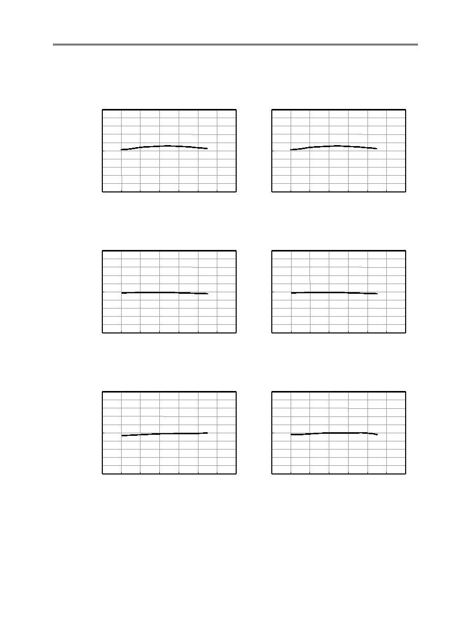
Characteristics
(typical characteristics)
Detection voltage temperature characteristics
4.15
4.25
4.35
-40
-20
0
20
40
60
80
100
V
CU
=4.25[V]
Ta(∞C)
V
CU
(V
)
Overcharge detection voltage vs. temperature
4.00
4.10
4.20
-40
-20
0
20
40
60
80
100
V
CD
=4.10[V]
Ta(∞C)
V
CD
(V
)
Overcharge release voltage vs. temperature
2.25
2.35
2.45
-40
-20
0
20
40
60
80
100
V
DD
=2.35[V]
Ta(∞C)
V
DD
(V
)
Overdischarge detection voltage vs. temperature
2.75
2.85
2.95
-40
-20
0
20
40
60
80
100
V
DU
=2.85[V]
Ta(∞C)
V
DU
(V
)
Overdischarge release voltage vs. temperature
0.25
0.30
0.35
-40
-20
0
20
40
60
80
100
V
IOV1
=0.3 [V]
Ta(∞C)
V
IO
V
1
(V
)
Overcurrent1 detection voltage vs. temperature
0.55
0.60
0.65
-40
-20
0
20
40
60
80
100
V
IOV2
=0.6 [V]
Ta(∞C)
V
IO
V
2
(V
)
Overcurrent2 detection voltage vs. temperature
Battery Protection IC(for a 3-serial-cell pack)
S-8233A Series
Rev.3.1_
00
Seiko Instruments Inc.
20
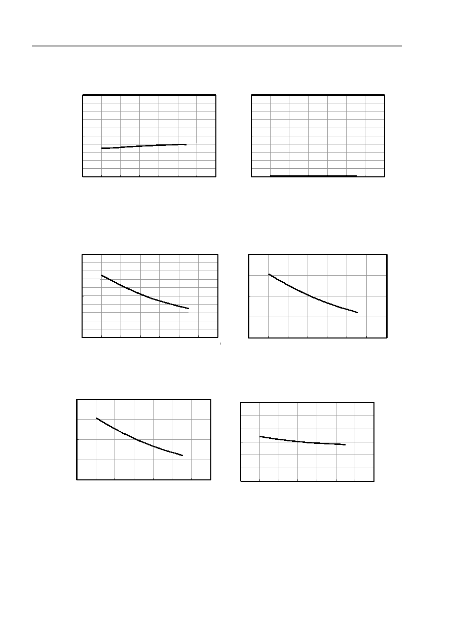
2. Current consumption temperature characteristics
0
25
50
-40
-20
0
20
40
60
80
100
V
CC
=10.5 [V]
Ta(∞C)
I
OPE
(uA
)
Current consumption vs. temperature in normal mode
0.0
0.5
1.0
-40
-20
0
20
40
60
80
100
V
CC
=4.5 [V]
Ta(∞C)
I
PD
N
(nA
)
Current consumption vs. temperature in power-down mode
3. Delay time temperature characteristics
0.5
1.0
1.5
-40
-20
0
20
40
60
80
100
C=0.47[uF]
V
CC
=11.5 [V]
Ta(∞C)
T
CU
(S
)
Overcharge detection time vs. temperature
20
40
60
-40
-20
0
20
40
60
80
100
C=0.1[uF]
V
CC
=8.5 [V]
Ta(∞C)
T
DD
(m
S
)
Overdischarge detection time vs. temperature
10
20
30
-40
-20
0
20
40
60
80
100
C=0.1[uF]
V
CC
=10.5 [V]
Ta(∞C)
T
IO
V
1
(m
S
)
Overcurrent1 detection time vs. temperature
2
5
8
-40
-20
0
20
40
60
80
100
V
CC
=10.5 [V]
Ta(∞C)
T
IO
V
2
(m
S
)
Overcurrent2 detection time vs. temperature

Battery Protection IC(for a 3-serial-cell pack)
Rev.3.1_
00
S-8233A Series
Seiko Instruments Inc.
21
0.10
0.25
0.40
-40
-20
0
20
40
60
80
100
V
CC
=6.0 [V]
Ta(∞C)
T
IO
V
3
(m
S
)
Overcurrent3 (load short) detection time vs. temperature
4. Delay time vs. power supply voltage
Over current 3 (load short) detection time vs. power
supply voltage
0.0
0.5
1.0
3
6
9
12
15
VCC [V]
TIOV3 [mS]
Ta=25[
∞C]
0.4
+0.1
-0.05
1.27
10.06 (10.5 max.)
0.2
+0.05
-0.02
No.
TITLE
SCALE
UNIT
mm
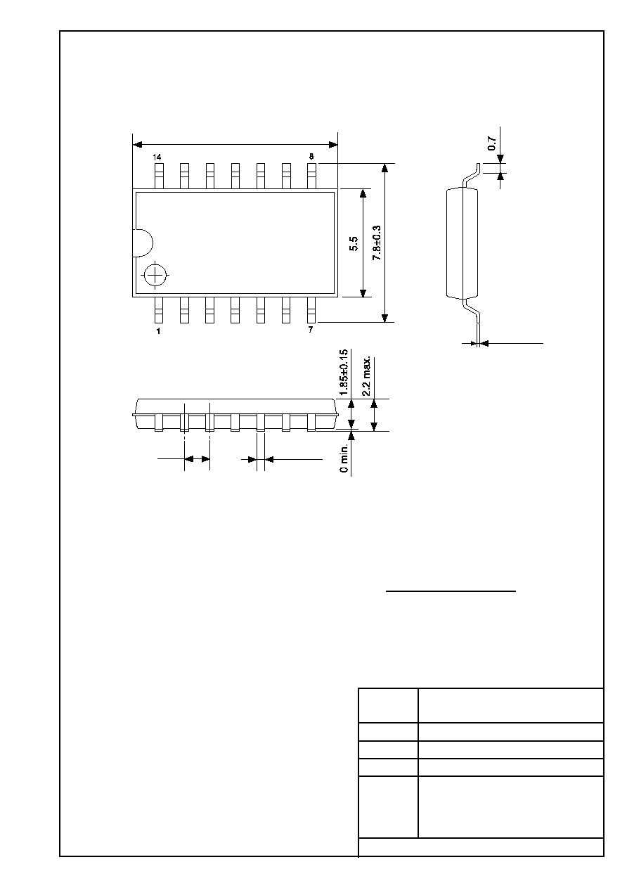
Seiko Instruments Inc.
SOP14-A-PKG Dimensions
No. FE014-A-P-SD-1.1
FE014-A-P-SD-1.1

8.8±0.1
5.4±0.2
8.5
+0.4
-0.2
2.7±0.1
0.3±0.05
4.0±0.1
2.0±0.1
¯1.5
+0.1
-0
¯1.6±0.1
12.0±0.1
No.
TITLE
SCALE
UNIT
mm
Seiko Instruments Inc.
(10 pitches:40.0±0.1)
SOP14-A-Carrier Tape
No. FE014-A-C-SD-1.1
FE014-A-C-SD-1.1
8
14
1
7
Feed direction
¯10
17.4±1.0
21.4±1.0
2.0±0.5
¯13.0±0.2
¯21.0±0.8
No.
TITLE
SCALE
UNIT
mm
QTY.
2,000
Seiko Instruments Inc.
Enlarged drawing in the central part
SOP14-A-Reel
No. FE014-A-R-SD-1.1
FE014-A-R-SD-1.1

∑
The information described herein is subject to change without notice.
∑
Seiko Instruments Inc. is not responsible for any problems caused by circuits or diagrams described herein
whose related industrial properties, patents, or other rights belong to third parties. The application circuit
examples explain typical applications of the products, and do not guarantee the success of any specific
mass-production design.
∑
When the products described herein are regulated products subject to the Wassenaar Arrangement or other
agreements, they may not be exported without authorization from the appropriate governmental authority.
∑
Use of the information described herein for other purposes and/or reproduction or copying without the
express permission of Seiko Instruments Inc. is strictly prohibited.
∑
The products described herein cannot be used as part of any device or equipment affecting the human
body, such as exercise equipment, medical equipment, security systems, gas equipment, or any apparatus
installed in airplanes and other vehicles, without prior written permission of Seiko Instruments Inc.
∑
Although Seiko Instruments Inc. exerts the greatest possible effort to ensure high quality and reliability, the
failure or malfunction of semiconductor products may occur. The user of these products should therefore
give thorough consideration to safety design, including redundancy, fire-prevention measures, and
malfunction prevention, to prevent any accidents, fires, or community damage that may ensue.