Document Outline
- S-8241 Series
- Cover
- Features
- Applications
- Packages
- Block Diagram
- Product Code Structure
- Pin Assignment
- Absolute Maximum Ratings
- Electrical Characteristics (1) Other than detection delay time (25∞C)
- Electrical Characteristics (2) Other than detection delay time (-40 to 85∞C)
- Electrical Characteristics (3) Detection delay time (25∞C)
- Electrical Characteristics (4) Detection delay time (-40 to 85∞C)
- Measurement Circuits
- Description of Operation
- Operation Timing Chart
- Battery Protection IC Connection Example
- Precautions
- Characteristic (typical characteristic)
- Package Drawing

Rev.3.8
_00
BATTERY PROTECTION IC
FOR A SINGLE CELL PACK
S-8241 Series
Seiko Instruments Inc.
1
The S-8241 Series is a series of lithium-ion/lithium polymer rechargeable
battery protection ICs incorporating high-accuracy voltage detection
circuits and delay circuits.
These ICs are suitable for protection of single-cell lithium ion/lithium
polymer battery packs from overcharge, overdischarge and overcurrent.
Features
(1) Internal high-accuracy voltage detection circuit
∑ Overcharge detection voltage: 3.9 V to 4.4 V (5 mV-step)
Accuracy of ± 25 mV(+25
∞C) and ± 30 mV(-5∞C to +55∞C)
∑ Overcharge release voltage
3.8 V to 4.4 V
*1
Accuracy of ±50 mV
*1. Overcharge release voltage = Overcharge detection voltage - Overcharge hysteresis
The overcharge hysteresis can be selected in the range 0.0, or 0.1 to 0.4 V in 50mV steps.
(However, selection "Overcharge release voltage<3.8 V" is enabled.)
∑ Overdischarge detection voltage: 2.0 V to 3.0 V (100 mV-step) Accuracy of ±80 mV
∑ Overdischarge release voltage:
2.0 V to 3.4 V
*2
Accuracy of ±100 mV
*2. Overdischarge release voltage = Overdischarge detection voltage + Overdischarge hysteresis
The overdischarge hysteresis can be selected in the range 0.0 to 0.7 V in 100mV steps.
(However, selection "Overdischarge release voltage
>3.4 V" is enabled.)
∑ Overcurrent 1 detection voltage: 0.05 V to 0.3 V (5 mV-step) Accuracy of ±20 mV
∑ Overcurrent 2 detection voltage: 0. 5 V (fixed) Accuracy of ±100 mV
(2) A high voltage withstand device is used for charger connection pins
(VM and CO pins: Absolute maximum rating = 26 V)
(3) Delay times (overcharge: t
CU
; overdischarge: t
DL
; overcurrent 1: t
lOV1
; overcurrent 2: t
lOV2
) are generated
by an internal circuit. (External capacitors are unnecessary.) Accuracy of ±30 %
(4) Internal three-step overcurrent detection circuit (overcurrent 1, overcurrent 2, and load short-circuiting)
(5) Either the 0 V battery charging function or 0 V battery charge inhibiting function can be selected.
(6) Products with and without a power-down function can be selected.
(7) Charger detection function and abnormal charge current detection function
∑ The overdischarge hysterisis is released by detecting a negative VM pin voltage (typ. -1.3 V). (Charger
detection function)
∑ If the output voltage at DO pin is high and the VM pin voltage becomes equal to or lower than the charger
detection voltage (typ. -1.3 V), the output voltage at CO pin goes low. (Abnormal charge current
detection function)
(8) Low current consumption
∑ Operation:
3.0
µA typ. 5.0 µA max.
∑ Power-down mode: 0.1 µA max.
(9) Wide operating temperature range:
-40 to +85 ∞C
(10) Small package
SOT-23-5, 5-Pin SON(A)
Applications
∑ Lithium-ion rechargeable battery packs
∑ Lithium- polymer rechargeable battery packs
Packages
∑ SOT-23-5 (PKG drawing code : MP005-A)
∑ 5-Pin SON(A) (PKG drawing code : PN005-A)
BATTERY PROTECTION IC FOR A SINGLE CELL PACK
S-8241 Series
Rev.3.8
_00
Seiko Instruments Inc.
2
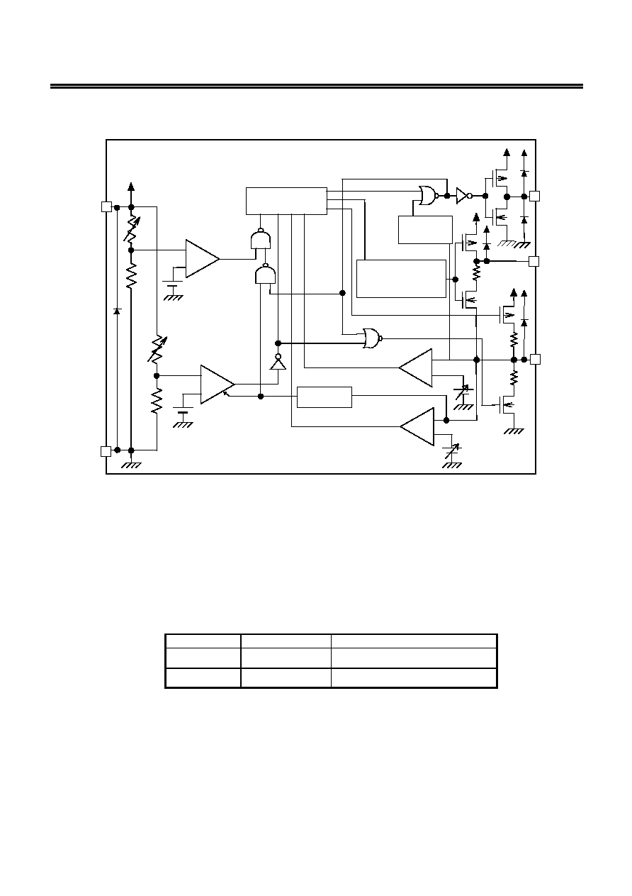
Block Diagram
+
-
-
+
VM
VSS
VDD
CO
DO
Overcharge
detection
comparator
Overcurrent 1
detection comparator
-
+
-
+
Overdischarge
detection
comparator
Overcurrent 2
detection comparator
Delay circuit
R
VMD
R
VMS
Counter circuit
Clock generation circuit
The overdischarge hysterisis
is released when a charger is
detected.
R
COL
Load short-
circuiting
detection circuit
Level conversion circuit
0V battery charging circuit
0V battery charge inhibition
circuit
Charger
detection circuit
Remark The diodes in the IC are parasitic diodes
Figure 1 Block Diagram
Product Code Structure
1. Product name
Product name: S-8241AB
-product code (GB
)-taping orientation (T2 or TF)
S-8241AC
-product code (GC
)-taping orientation (T2 or TF)
Symbol Meaning
Description
Serial number
Is set from A to Z in sequence.
Package form
MC:SOT-23-5, PN:5-pin SON(A)

BATTERY PROTECTION IC FOR A SINGLE CELL PACK
Rev.3.8
_00
S-8241 Series
Seiko Instruments Inc.
3
2. Product name list
Model No./Item
Over-
charge
detection
voltage
[V
CU
]
Over-
charge
release
voltage
[V
CL
]
Over-
discharge
detection
voltage
[V
DL
]
Over-
discharge
release
voltage
[V
DU
]
Over-
current 1
detection
voltage
[V
IOV1
]
0V battery
charging
function
Delay
time
combi-
nation
*1
Power down
function
S-8241ABAMC-GBA-T2
4.275 V
4.075 V
2.3 V
2.9 V
0.100 V
Unavailable
(1)
Available
S-8241ABBMC-GBB-T2
4.280 V
3.980 V
2.3 V
2.4 V
0.125 V
Available
(2)
Available
S-8241ABCMC-GBC-T2
4.350 V
4.100 V
2.3 V
2.8 V
0.075 V
Unavailable
(1)
Available
S-8241ABDMC-GBD-T2
4.275 V
4.175 V
2.3 V
2.4 V
0.100 V
Available
(1)
Available
S-8241ABDPN-KBD-TF
S-8241ABEMC-GBE-T2
4.295 V
4.095 V
2.3 V
3.0 V
0.200 V
Unavailable
(1)
Available
S-8241ABFMC-GBF-T2
4.325 V
4.075 V
2.5 V
2.9 V
0.100 V
Unavailable
(1)
Available
S-8241ABGMC-GBG-T2
4.200 V
4.100 V
2.3 V
3.0 V
0.100 V
Unavailable
(1)
Available
S-8241ABHMC-GBH-T2
4.325 V
4.125 V
2.3 V
2.3 V
0.100 V
Available
(1)
Available
S-8241ABIMC-GBI-T2
4.280 V
4.080 V
2.3 V
2.3 V
0.160 V
Unavailable
(1)
Available
S-8241ABKMC-GBK-T2
4.325 V
4.075 V
2.5 V
2.9 V
0.150 V
Unavailable
(1)
Available
S-8241ABLMC-GBL-T2
4.320 V
4.070 V
2.5 V
2.9 V
0.100 V
Unavailable
(1)
Available
S-8241ABNPN-KBN-TF 4.350V 4.050V 2.35V 2.65V 0.150V Available (1) Available
S-8241ABOMC-GBO-T2 4.350V 4.15V 2.3V
3.0V 0.150V Available (2) Available
S-8241ABPMC-GBP-T2 4.350V 4.15V 2.3V
3.0V 0.200
V Available (2) Available
S-8241ABQMC-GBQ-T2 4.280V 4.080V 2.3V
2.3V 0.130
V Unavailable (1) Available
S-8241ABSPN-KBS-TF 4.350V 4.150V 2.35V 2.65V 0.200
V Available (2) Available
S-8241ABTPN-KBT-TF 4.300V 4.100V 2.3V 2.3V 0.100
V Available (1) Available
S-8241ABUMC-GBU-T2 4.200V 4.100V 2.3V
2.3V 0.150
V Unavailable (1) Available
S-8241ABVMC-GBV-T2 4.295V 4.095V 2.3V
2.3V 0.130
V Available (1) Available
S-8241ABWMC-GBW-T2 4.280V 4.080V 2.3V
2.3V 0.130
V Unavailable (3) Available
S-8241ABXMC-GBX-T2 4.350V 4.000V 2.6V
3.3V 0.200
V Unavailable (1) Available
S-8241ABXPN-KBX-TF
S-8241ABYMC-GBY-T2
4.220 V
4.220 V
2.3 V
2.3 V
0.200 V
Available
(3)
Available
S-8241ABZPN-KBZ-TF
4.275 V
4.075 V
2.3 V
2.4 V
0.140 V
Available
(1)
Available
S-8241ACAMC-GCA-T2
4.280 V
4.080 V
2.3 V
2.3 V
0.200 V
Available
(1)
Available
S-8241ACAPN-KCA-TF
S-8241ACBMC-GCB-T2
4.300 V
4.100 V
2.3 V
2.3 V
0.150 V
Available
(1)
Available
S-8241ACDMC-GCD-T2
4.275 V
4.075 V
2.3 V
2.3 V
0.100 V
Unavailable
(4)
Available
S-8241ACEMC-GCE-T2
4.295 V
4.095 V
2.3 V
2.3 V
0.080 V
Available
(1)
Available
S-8241ACFMC-GCF-T2
4.295 V
4.095 V
2.3 V
2.3 V
0.090 V
Available
(1)
Available
S-8241ACGMC-GCG-T2
4.295 V
4.095 V
2.3 V
2.3 V
0.060 V
Available
(1)
Available
S-8241ACGPN-KCG-TF
S-8241ACHMC-GCH-T2
4.280 V
4.080 V
2.6 V
2.6 V
0.200 V
Available
(1)
Available
S-8241ACIMC-GCI-T2
4.350 V
4.150 V
2.05 V
2.75 V
0.200 V
Available
(2)
Available
S-8241ACJPN-KCJ-TF 4.300V 4.100V 2.3V 2.3V 0.120V Available (1) Available
S-8241ACKMC-GCK-T2 4.350V 4.150V 2.0V
2.0V 0.200V Available (2) Available
S-8241ACLMC-GCL-T2 4.200V 4.200V 2.5V
3.0V 0.100V Available (1) Available
S-8241ACNMC-GCN-T2 4.350V 4.150V 2.1V
2.2V 0.200V Available (2) Available

BATTERY PROTECTION IC FOR A SINGLE CELL PACK
S-8241 Series
Rev.3.8
_00
Seiko Instruments Inc.
4
Model No./Item
Over-
charge
detection
voltage
[V
CU
]
Over-
charge
release
voltage
[V
CL
]
Over-
discharge
detection
voltage
[V
DL
]
Over-
discharge
release
voltage
[V
DU
]
Over-
current 1
detection
voltage
[V
IOV1
]
0V battery
charging
function
Delay
time
combi-
nation
*1
Power down
function
S-8241ACOMC-GCO-T2
4.100 V
3.850 V
2.5 V
2.9 V
0.150 V
Unavailable
(1)
Unavailable
S-8241ACPMC-GCP-T2
4.325 V
4.075 V
2.5 V
2.9 V
0.150 V
Unavailable
(1)
Unavailable
S-8241ACQMC-GCQ-T2
4.275 V
4.175 V
2.3 V
2.4 V
0.100 V
Available
(1)
Unavailable
S-8241ACRMC-GCR-T2
4.350 V
4.150 V
2.3 V
3.0 V
0.100 V
Available
(1)
Unavailable
S-8241ACSMC-GCS-T2
4.180 V
3.930 V
2.5 V
2.9 V
0.150 V
Unavailable
(1)
Unavailable
S-8241ACTMC-GCT-T2
4.100 V
4.000 V
2.5 V
2.9 V
0.150 V
Unavailable
(1)
Unavailable
S-8241ACUMC-GCU-T2
4.180 V
4.080 V
2.5 V
2.9 V
0.150 V
Unavailable
(1)
Unavailable
S-8241ACWMC-GCW-T2
4.350 V
4.150 V
2.3 V
3.0 V
0.200 V
Available
(2)
Unavailable
*1. The delay time combination (1), (2), (3), (4) is as follows.
Delay time
combination
Overcharge detection
delay time
Overdischarge detection
delay time
Overcurrent 1 detection
delay time
(1)
1.0 s
125 ms
8 ms
(2)
0.125 s
31 ms
16 ms
(3)
0.25 s
125 ms
8 ms
(4)
2.0 s
125 ms
8 ms
It is possible to change the detection voltage for products other than those listed above. Also, delay time can be
changed within the following range. For details, please contact our sales office.
Delay time
Symbol
Optional range
Remarks
Overcharge detection
delay time
t
CU
0.25 s
0.5 s
1.0 s
Choose from the list at left.
Overdischarge detection
delay time
t
DL
31 ms
62.5 ms
125 ms
Choose from the list at left.
Overcurrent 1 detection
delay time
t
lOV1
4
ms
8 ms
16 ms
Choose from the list at left.
Shaded boxes indicate standard values.
BATTERY PROTECTION IC FOR A SINGLE CELL PACK
Rev.3.8
_00
S-8241 Series
Seiko Instruments Inc.
5
Pin Assignment
Pin
No.
Symbol
Description
1 VM
Voltage detection pin between VM and VSS
(Overcurrent detection pin)
2 VDD
Positive power input pin
3 VSS
Negative power input pin
4 DO
FET gate connection pin for discharge control
(CMOS output)
5 CO
FET gate connection pin for charge control
(CMOS output)
5 4
1 3
2
SOT-23-5
Top view
Figure 2
Pin
No.
Symbol
Description
1 VM
Voltage detection pin between VM and VSS
(Overcurrent detection pin)
2 VDD
Positive power input pin
3 CO
FET gate connection pin for charge control
(CMOS output)
4 DO
FET gate connection pin for discharge control
(CMOS output)
5 VSS
Negative power input pin
Remark Pin assignment of SOT-23-5 and of 5-Pin SON(A) are different.
3
2
1
4
5
5-Pin SON(A)
Top view
Figure 3
Absolute Maximum Ratings
(Ta = 25
∞C unless otherwise specified)
Item Symbol
Applicable
pin
Rating
Unit
Input voltage between VDD and VSS
*1
V
DS
VDD V
SS
-0.3 to V
SS
+12
V
VM Input pin voltage
V
VM
VM V
DD
-26 to V
DD
+0.3
V
CO output pin voltage
V
CO
CO V
VM
-0.3 to V
DD
+0.3
V
DO output pin voltage
V
DO
DO V
SS
-0.3 to V
DD
+0.3
V
Power dissipation
SOT-23-5
P
D
- 250
mW
5-Pin
SON(B)
150
Operating temperature range
Topr
-
-40 to +85
∞C
Storage temperature range
Tstg
-
-40 to +125
∞C
*1. Do not apply pulse-like noise of
µs order exceeding the above input voltage (V
SS
+ 12 V). The noise causes
damage to the IC.
Caution The absolute maximum ratings are rated values exceeding which the product could suffer
physical damage. These values must therefore not be exceeded under any conditions.

BATTERY PROTECTION IC FOR A SINGLE CELL PACK
S-8241 Series
Rev.3.8
_00
Seiko Instruments Inc.
6
Electrical Characteristics (1) Other than detection delay time (25
∞
∞
∞
∞C)
(Ta = 25
∞C unless otherwise specified)
Item Symbol
Measure-
ment
conditions
Remarks Min.
Typ.
Max.
Unit
Measure
-ment
circuit
DETECTION VOLTAGE
V
CU
1
-
V
CU
-0.025 V
CU
V
CU
+0.025 V
1
Overcharge detection voltage
V
CU
=3.9 to 4.4 V, 5 mV Step
Ta=
-5
∞C to 55∞C
*1
V
CU
-0.030 V
CU
V
CU
+0.030
V
CL
1
When
V
CL
V
CU
V
CL
-0.050 V
CL
V
CL
+0.050 V
1
Overcharge release voltage
V
CU
-V
CL
=0 to 0.4 V, 50mV Step
When
V
CL
= V
CU
V
CL
-0.025 V
CL
V
CL
+0.025
Overdischarge detection voltage
V
DL
=2.0 to 3.0 V, 100mV Step
V
DL
1
-
V
DL
-0.080 V
DL
V
DL
+0.080 V
1
V
DU
1
When
V
DU
V
DL
V
DU
-0.100 V
DU
V
DU
+0.100
Overdischarge release voltage
V
DU
-V
DL
=0 to 0.7 V, 100mV Step
When
V
DU
= V
DL
V
DU
-0.080 V
DU
V
DU
+0.080 V
1
Overcurrent 1 detection voltage
V
IOV1
=0.05 to 0.3V, 5mV Step
V
IOV1
2
-
V
IOV1
-0.020 V
IOV1
V
IOV1
+0.02
0
V 1
Overcurrent 2 detection voltage
V
IOV2
2
-
0.4 0.5 0.6 V 1
Load short-circuiting detection
voltage
V
SHORT
2
VM voltage based on V
DD
-1.7
-1.3
-0.9
V
1
Charger detection voltage
V
CHA
3
- -2.0
-1.3
-0.6
V
1
Overcharge detection voltage
temperature factor
*1
T
COE1
- Ta=
-5
∞C to 55∞C -0.5
0
0.5
mV/
∞C
-
Overcurrent 1 detection voltage
temperature factor
*1
T
COE2
- Ta=
-5
∞C to 55∞C -0.1
0
0.1
mV/
∞C
-
INPUT VOLTAGE, OPERATING VOLTAGE
Input voltage between VDD and
VSS
V
DS1
-
absolute maximum rating
-0.3
- 12 V -
Input voltage between VDD and VM
V
DS2
-
absolute maximum rating
-0.3
- 26 V -
Operating voltage between VDD
and VSS
V
DSOP1
-
Internal circuit operating voltage
1.5
- 8 V
-
Operating voltage between VDD
and VM
V
DSOP2
-
Internal circuit operating voltage
1.5
- 24 V -
CURRENT CONSUMPTION Power-down function available
Current consumption during normal
operation
I
OPE
4
V
DD
=3.5V, V
VM
=0 V
1.0
3.0
5.0
µA 1
Current consumption at power
down
I
PDN
4
V
DD
=V
VM
=1.5 V
-
- 0.1 µA 1
CURRENT CONSUMPTION Power-down function unavailable
Current consumption during normal
operation
I
OPE
4
V
DD
=3.5 V, V
VM
=0 V
1.0
3.0
5.0
µA 1
Overdischarge current consumption
I
OPED
4
V
DD
=V
VM
=1.5 V
1.0
2.0
3.5
µA 1
OUTPUT RESISTANCE
CO pin H resistance
R
COH
6 V
CO
=3.0 V,V
DD
=3.5 V,V
VM
=0 V
0.1
2
10
k
1
CO pin L resistance
R
COL
6 V
CO
=0.5 V,V
DD
=4.5 V,V
VM
=0 V
150
600
2400
k
1
DO pin H resistance
R
DOH
7 V
DO
=3.0 V,V
DD
=3.5 V,V
VM
=0 V
0.1
1.3
6.0
k
1
DO pin L resistance
R
DOL
7 V
DO
=0.5 V,V
DD
=V
VM
=1.8 V
0.1
0.5
2.0
k
1
VM INTERNAL RESISTANCE
Internal resistance between VM and
VDD
R
VMD
5
V
DD
=1.8 V, V
VM
=0 V
100
300
900
k
1
Internal resistance between VM and
VSS
R
VMS
5
V
DD
=V
VM
=3.5 V
50
100
150
k
1
0 V BATTERY CHARGING FUNCTION
The 0 V battery function is either "0 V battery charging function" or "0 V battery charge inhibiting function"
depending upon the product type.
0 V battery charge starting charger
voltage
V
0CHA
10
0 V battery charging Available
0.0
0.8
1.5
V
1
0 V battery charge inhibiting battery
voltage
V
0INH
11
0 V battery charging Unavailable
0.6
0.9
1.2
V
1
*1. Since products are not screened at high and low temperatures, the specification for this temperature range is guaranteed by design, not tested in
production.

BATTERY PROTECTION IC FOR A SINGLE CELL PACK
Rev.3.8
_00
S-8241 Series
Seiko Instruments Inc.
7
Electrical Characteristics (2) Other than detection delay time (-40 to 85
∞
∞
∞
∞C)
*1
(Ta = (-40 to 85
∞C
*1
)unless otherwise specified)
Item Symbol
Measure-
ment
conditions
Remarks Min.
Typ.
Max.
Unit
Measure
-ment
circuit
DETECTION VOLTAGE
Overcharge detection voltage
V
CU
=3.9 to 4.4 V, 5mV Step
V
CU
1
-
V
CU
-0.055 V
CU
V
CU
+0.040 V 1
V
CL
1
When
V
CL
V
CU
V
CL
-0.095 V
CL
V
CL
+0.060 V 1
Overcharge release voltage
V
CU
-V
CL
=0 to 0.4 V, 50mV Step
When
V
CL
= V
CU
V
CL
-0.055 V
CL
V
CL
+0.040
Overdischarge detection voltage
V
DL
=2.0 to 3.0 V, 100mV Step
V
DL
1
-
V
DL
-0.120 V
DL
V
DL
+0.120 V 1
V
DU
1
When
V
DU
V
DL
V
DU
-0.140 V
DU
V
DU
+0.140 V 1
Overdischarge release voltage
V
DU
-V
DL
=0 to 0.7 V, 100mV Step
When
V
DU
= V
DL
V
DU
-0.120 V
DU
V
DU
+0.120
Overcurrent 1 detection voltage
V
IOV1
=0.05 to 0.3V, 5mV Step
V
IOV1
2
-
V
IOV1
-0.026 V
IOV1
V
IOV1
+0.026 V
1
Overcurrent 2 detection voltage
V
IOV2
2
- 0.37
0.5
0.63
V
1
Load short-circuiting detection
voltage
V
SHORT
2
VM voltage based on V
DD
-1.9
-1.3 -0.7 V 1
Charger detection voltage
V
CHA
3
- -2.2
-1.3
-0.4
V
1
Overcharge detection voltage
temperature factor
*1
T
COE1
- Ta=
-40
∞C to 85∞C -0.7
0
0.7
mV/
∞C
-
Overcurrent 1 detection voltage
temperature factor
*1
T
COE2
- Ta=
-40
∞C to 85∞C -0.2
0
0.2
mV/
∞C
-
INPUT VOLTAGE, OPERATING VOLTAGE
Input voltage between VDD and
VSS
V
DS1
-
absolute maximum rating
-0.3
- 12 V -
Input voltage between VDD and VM
V
DS2
-
absolute maximum rating
-0.3
- 26 V -
Operating voltage between VDD
and VSS
V
DSOP1
-
Internal circuit operating voltage
1.5
- 8 V
-
Operating voltage between VDD
and VM
V
DSOP2
-
Internal circuit operating voltage
1.5
- 24 V -
CURRENT CONSUMPTION Power-down function available
Current consumption during normal
operation
I
OPE
4
V
DD
=3.5 V, V
VM
=0 V
0.7
3.0
6.0
µA 1
Current consumption at power
down
I
PDN
4
V
DD
=V
VM
=1.5 V
-
- 0.1 µA 1
CURRENT CONSUMPTION Power-down function unavailable
Current consumption during normal
operation
I
OPE
4
V
DD
=3.5 V, V
VM
=0 V
0.7
3.0
6.0
µA 1
Overdischarge current consumption
I
OPED
4
V
DD
=V
VM
=1.5 V
0.6
2.0
4.5
µA 1
OUTPUT RESISTANCE
CO pin H resistance
R
COH
6 V
CO
=3.0 V,V
DD
=3.5 V,V
VM
=0 V
0.07
2
13
k
1
CO pin L resistance
R
COL
6 V
CO
=0.5 V,V
DD
=4.5 V,V
VM
=0
V 100 600 3500 k
1
DO pin H resistance
R
DOH
7 V
DO
=3.0 V,V
DD
=3.5 V,V
VM
=0 V
0.07
1.3
7.3
k
1
DO pin L resistance
R
DOL
7 V
DO
=0.5 V,V
DD
=V
VM
=1.8 V
0.07
0.5
2.5
k
1
VM INTERNAL RESISTANCE
Internal resistance between VM and
VDD
R
VMD
5
V
DD
=1.8 V, V
VM
=0
V
78 300 1310 k
1
Internal resistance between VM and
VSS
R
VMS
5
V
DD
=V
VM
=3.5 V
39
100
220
k
1
0 V BATTERY CHARGING FUNCTION
The 0 V battery function is either "0 V battery charging function" or "0 V battery charge inhibiting function"
depending upon the product type.
0 V battery charge starting charger
voltage
V
0CHA
10
0 V battery charging Available
0.0
0.8
1.7
V
1
0 V battery charge inhibiting battery
voltage
V
0INH
11
0 V battery charging Unavailable
0.4
0.9
1.4
V
1
*1. Since products are not screened at high and low temperatures, the specification for this temperature range is guaranteed by design,
not tested in production.

BATTERY PROTECTION IC FOR A SINGLE CELL PACK
S-8241 Series
Rev.3.8
_00
Seiko Instruments Inc.
8
Electrical Characteristics (3) Detection delay time (25
∞
∞
∞
∞C)
(Ta = 25
∞C unless otherwise specified)
Item Symbol
Measurement
conditions
Remarks Min. Typ. Max. Unit
Measurement
circuit
DELAY TIME
(1)
Overcharge detection delay time
t
CU
8
-
0.7 1.0 1.3 s
1
Overdischarge detection delay time
t
DL
8
-
87.5 125 162.5 ms
1
Overcurrent 1 detection delay time
t
lOV1
9
-
5.6 8 10.4
ms
1
Overcurrent 2 detection delay time
t
lOV2
9
-
1.4 2 2.6 ms
1
Load short-circuiting detection delay time t
SHORT
9
-
-
10 50
µs
1
DELAY TIME
(2)
Overcharge detection delay time
t
CU
8
-
87.5 125 162.5 ms
1
Overdischarge detection delay time
t
DL
8
-
21 31 41 ms
1
Overcurrent 1 detection delay time
t
lOV1
9
-
11 16 21 ms
1
Overcurrent 2 detection delay time
t
lOV2
9
-
1.4 2 2.6 ms
1
Load short-circuiting detection delay time t
SHORT
9
-
-
10 50
µs
1
DELAY TIME
(3)
Overcharge detection delay time
t
CU
8
-
0.175 0.25 0.325 s
1
Overdischarge detection delay time
t
DL
8
-
87.5 125 162.5 ms
1
Overcurrent 1 detection delay time
t
lOV1
9
-
5.6 8 10.4
ms
1
Overcurrent 2 detection delay time
t
lOV2
9
-
1.4 2 2.6 ms
1
DELAY TIME
(4)
Overcharge detection delay time
t
CU
8
-
1.4 2.0 2.6 s
1
Overdischarge detection delay time
t
DL
8
-
87.5 125 162.5 ms
1
Overcurrent 1 detection delay time
t
lOV1
9
-
5.6 8 10.4
ms
1
Overcurrent 2 detection delay time
t
lOV2
9
-
1.4 2 2.6 ms
1
Load short-circuiting detection delay time t
SHORT
9
-
-
10 50
µs
1

BATTERY PROTECTION IC FOR A SINGLE CELL PACK
Rev.3.8
_00
S-8241 Series
Seiko Instruments Inc.
9
Electrical Characteristics (4) Detection delay time (-40 to 85
∞
∞
∞
∞C)
*1
(Ta = -40 to 85
∞C
*1
unless otherwise specified)
Item Symbol
Measurement
conditions
Remarks Min. Typ. Max. Unit
Measurement
circuit
DELAY TIME (1)
Overcharge detection delay time
t
CU
8
-
0.55 1.0 1.7 s
1
Overdischarge detection delay time
t
DL
8
-
69 125 212 ms
1
Overcurrent 1 detection delay time
t
IOV1
9
-
4.4 8 14 ms
1
Overcurrent 2 detection delay time
t
IOV2
9
-
1.1 2 3.4 ms
1
Load short-circuiting detection delay
time
t
SHORT
9
-
-
10 73
µs
1
DELAY TIME (2)
Overcharge detection delay time
t
CU
8
-
69 125 212 ms
1
Overdischarge detection delay time
t
DL
8
-
17 31 53 ms
1
Overcurrent 1 detection delay time
t
IOV1
9
-
9 16 27 ms 1
Overcurrent 2 detection delay time
t
IOV2
9
-
1.1 2 3.4 ms
1
Load short-circuiting detection delay time t
SHORT
9
-
-
10 73
µs
1
DELAY TIME (3)
Overcharge detection delay time
t
CU
8
-
0.138 0.25 0.425 s
1
Overdischarge detection delay time
t
DL
8
-
69 125 212 ms
1
Overcurrent 1 detection delay time
t
IOV1
9
-
4.4 8 14 ms
1
Overcurrent 2 detection delay time
t
IOV2
9
-
1.1 2 3.4 ms
1
Load short-circuiting detection delay time t
SHORT
9
-
-
10 73
µs
1
DELAY TIME (4)
Overcharge detection delay time
t
CU
8
-
1.1 2.0 3.4 s
1
Overdischarge detection delay time
t
DL
8
-
69 125 212 ms
1
Overcurrent 1 detection delay time
t
IOV1
9
-
4.4 8 14 ms
1
Overcurrent 2 detection delay time
t
IOV2
9
-
1.1 2 3.4 ms
1
Load short-circuiting detection delay time t
SHORT
9
-
-
10 73
µs
1
*1. Since products are not screened at high and low temperatures, the specification for this temperature range is guaranteed by design, not
tested in production.

BATTERY PROTECTION IC FOR A SINGLE CELL PACK
S-8241 Series
Rev.3.8
_00
Seiko Instruments Inc.
10
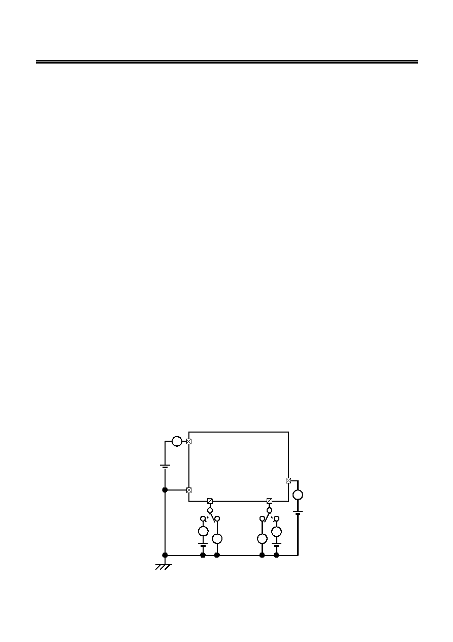
Measurement Circuits
Unless otherwise specified, the output voltage levels "H" and "L" at CO and DO pins are judged by the
threshold voltage (1.0 V) of a Nch FET. Judge the CO pin level with respect to V
VM
and the DO pin level with
respect to V
SS
. Voltages V1 to V4 are shown in the figure 4.
(1) Measurement Condition 1, Measurement Circuit 1
Overcharge detection voltage, Overcharge release voltage, Overdischarge detection voltage,
Overdischarge release voltage
The overcharge detection voltage (V
CU
) is defined by the voltage between VDD and VSS at which V
CO
goes
L from H when the voltage V1 is gradually increased from the normal condition V1=3.5 V and
V2=0 V. The overcharge release voltage (V
CL
) is defined by the voltage between VDD and VSS at which
V
CO
goes
H from L when the voltage V1 is then gradually decreased.
Gradually decreasing the voltage V1, the overdischarge detection voltage (V
DL
) is defined by the voltage
between VDD and VSS at which V
DO
goes
L from H. The overdischarge release voltage (V
DU
) is
defined by the voltage between VDD and VSS at which V
DO
goes
H from L when the voltage V1 is then
gradually increased.
(2) Measurement Condition 2, Measurement Circuit 1
Overcurrent 1 detection voltage, Overcurrent 2 detection voltage, Load short-circuiting detection
voltage
The overcurrent 1 detection voltage (V
IOV1
) is defined by the voltage between VDD and VSS at which V
DO
goes
L from H when the voltage V2 is gradually increased from the normal condition V1=3.5 V and
V2=0 V.
The overcurrent 2 detection voltage (V
IOV2
) is defined by the voltage between VDD and VSS at which V
DO
goes
L from H when the voltage V2 is increased at the speed between 1 ms and 4 ms from the normal
condition V1=3.5 V and V2=0 V.
The load short-circuiting detection voltage (V
SHORT
) is defined by the voltage between VDD and VSS at
which V
DO
goes
L from H when the voltage V2 is increased at the speed between 1 µs and 50 µs from
the normal condition V1=3.5 V and V2=0 V.
(3) Measurement Condition 3, Measurement Circuit 1
Charger detection voltage, (=abnormal charge current detection voltage)
∑ Applied only for products with overdischarge hysteresis
Set V1=1.8 V and V2=0 V under overdischarge condition. Increase V1 gradually, set V1=(V
DU
+V
DL
)/2
(within overdischarge hysteresis, overdischarge condition), then decrease V2 from 0 V gradually. The
voltage between VM and VSS at which V
DO
goes
H from L is the charger detection voltage (V
CHA
).
∑ Applied only for products without overdischarge hysteresis
Set V1=3.5 V and V2=0 V under normal condition. Decrease V2 from 0 V gradually. The voltage between
VM and VSS at which V
CO
goes
L from H is the abnormal charge current detection voltage. The
abnormal charge current detection voltage has the same value as the charger detection voltage (V
CHA
).

BATTERY PROTECTION IC FOR A SINGLE CELL PACK
Rev.3.8
_00
S-8241 Series
Seiko Instruments Inc.
11
(4) Measurement Condition 4, Measurement Circuit 1
Normal operation current consumption, Power-down current consumption, Overdischarge current
consumption
Set V1=3.5 V and V2=0 V under normal condition. The current I
DD
flowing through VDD pin is the normal
operation consumption current (I
OPE
).
∑ For products with power-down function
Set V1=V2=1.5 V under overdischarge condition. The current I
DD
flowing through VDD pin is the
power-down current consumption (I
PDN
).
∑ For products without power-down function
Set V1=V2=1.5 V under overdischarge condition. The current I
DD
flowing through VDD pin is the
overdischarge current consumption (I
OPED
).
(5) Measurement Condition 5, Measurement Circuit 1
Internal resistance between VM and VDD, Internal resistance between VM and VSS
Set V1=1.8 V and V2=0 V under overdischarge condition. Measure current I
VM
flowing through VM pin.
1.8V/|I
VM
| gives the internal resistance (R
VMD
) between VM and VDD.
Set V1=V2=3.5 V under overcurrent condition. Measure current I
VM
flowing through VM pin. 3.5 V/|I
VM
|
gives the internal resistance (R
VMS
) between VM and VSS.
(6) Measurement Condition 6, Measurement Circuit 1
CO pin H resistance, CO pin L resistance
Set V1=3.5 V, V2=0 V and V3=3.0 V under normal condition. Measure current I
CO
flowing through CO pin.
0.5 V/|I
CO
| is the CO pin H resistance (R
COH
).
Set V1=4.5 V, V2=0 V and V3=0.5 V under overcharge condition. Measure current I
CO
flowing through
CO pin. 0.5 V/|I
CO
| is the CO pin L resistance (R
COL
).
(7) Measurement Condition 7, Measurement Circuit 1
DO pin H resistance, DO pin L resistance
Set V1=3.5 V, V2=0 V and V4=3.0 V under normal condition. Measure current I
DO
flowing through DO pin.
0.5V/|I
DO
| gives the DO pin H resistance (R
DOH
).
Set V1=1.8 V, V2=0 V and V4=0.5 V under overdischarge condition. Measure current I
DO
flowing through
DO pin. 0.5 V/|I
DO
| gives the DO pin L resistance (R
DOL
).
(8) Measurement Condition 8, Measurement Circuit 1
Overcharge detection delay time, Overdischarge detection delay time
Set V1=3.5 V and V2=0 V under normal condition. Increase V1 gradually to overcharge detection voltage
V
CU
- 0.2 V and increase V1 to the overcharge detection voltage V
CU
+ 0.2 V momentarily (within 10
µs).
The time after V1 becomes the overcharge detection voltage until V
CO
goes "L" is the overcharge
detection delay time (t
CU
).
Set V1=3.5 V and V2=0 V under normal condition. Decrease V1 gradually to overdischarge detection
voltage V
DL
+ 0.2 V and decrease V1 to the overdischarge detection voltage V
DL
- 0.2 V momentarily
(within 10
µs). The time after V1 becomes the overdischarge detection voltage V
DL
until V
DO
goes "L" is
the overdischarge detection delay time (t
DL
).
BATTERY PROTECTION IC FOR A SINGLE CELL PACK
S-8241 Series
Rev.3.8
_00
Seiko Instruments Inc.
12
(9) Measurement Condition 9, Measurement Circuit 1
Overcurrent 1 detection delay time, Overcurrent 2 detection delay time, Load short-circuiting detection
delay time, Abnormal charge current detection delay time
Set V1=3.5V and V2=0V under normal condition. Increase V2 from 0 V to 0.35 V momentarily (within
10
µs). The time after V2 becomes overcurrent 1 detection voltage (V
IOV1
) until V
DO
goes "L" is
overcurrent 1 detection delay time (t
IOV1
).
Set V1=3.5 V and V2=0 V under normal condition. Increase V2 from 0 V to 0.7 V momentarily (within
1
µs). The time after V2 becomes overcurrent 1 detection voltage (V
IOV1
) until V
DO
goes "L" is overcurrent
2 detection delay time (t
IOV2
).
Note: The overcurrent 2 detection delay time starts when the overcurrent 1 is detected, since the delay circuit is
common.
Set V1=3.5 V and V2=0 V under normal condition. Increase V2 from 0 V to 3.0 V momentarily (within
1
µs). The time after V2 becomes the load short-circuiting detection voltage (V
SHORT
) until V
DO
goes "L" is
the load short-circuiting detection delay time (t
SHORT
).
Set V1=3.5 V and V2=0 V under normal condition. Decrease V2 from 0 V to -2.5 V momentarily (within
10
µs). The time after V2 becomes the charger detection voltage (V
CHA
) until V
CO
goes "L" is the abnormal
charge current detection delay time. The abnormal charge current detection delay time has the same
value as the overcharge detection delay time.
(10) Measurement Condition 10, Measurement Circuit 1 (Product with 0V battery charging function)
0V battery charge start charger voltage
Set V1=V2=0 V and decrease V2 gradually. The voltage between VDD and VM at which V
CO
goes
H
(V
VM
+ 0.1 V or higher) is the 0 V battery charge start charger voltage (V
0CHA
).
(11) Measurement Condition 11, Measurement Circuit 1 (Product with 0V battery charge inhibiting function)
0V battery charge inhibiting battery voltage
Set V1=0 V and V2=-4 V. Increase V1 gradually. The voltage between VDD and VSS at which V
CO
goes
H (V
VM
+ 0.1 V or higher) is the 0V battery charge inhibiting battery voltage (V
0INH
).
VSS
DO
CO
VDD
S-8241 series
V1
I
DD
VM
V2
Measurement circuit 1
I
VM
A
V
A
V
DO
COM
A
I
DO
V
V
CO
A
I
CO
V4 V3
Figure 4

BATTERY PROTECTION IC FOR A SINGLE CELL PACK
Rev.3.8
_00
S-8241 Series
Seiko Instruments Inc.
13
Description of Operation
Normal condition
The S-8241 monitors the voltage of the battery connected to VDD and VSS pins and the voltage
difference between VM and VSS pins to control charging and discharging. When the battery voltage is in
the range from the overdischarge detection voltage (V
DL
) to the overcharge detection voltage (V
CU
), and
the VM pin voltage is in the range from the charger detection voltage (V
CHA
) to the overcurrent 1 detection
voltage (V
IOV1
) (the current flowing through the battery is equal to or lower than a specified value), the IC
turns both the charging and discharging control FETs on. This condition is called normal condition and in
this condition charging and discharging can be carried out freely.
Overcurrent condition
When the discharging current becomes equal to or higher than a specified value (the VM pin voltage is
equal to or higher than the overcurrent detection voltage) during discharging under normal condition and
the state continues for the overcurrent detection delay time or longer, the S-8241 turns the discharging
control FET off to stop discharging. This condition is called overcurrent condition. (The overcurrent
includes overcurrent 1, overcurrent 2, or load short-circuiting.)
The VM and VSS pins are shorted internally by the R
VMS
resistor under the overcurrent condition. When
a load is connected, the VM pin voltage equals the V
DD
voltage due to the load.
The overcurrent condition returns to the normal condition when the load is released and the impedance
between the EB+ and EB- pins (see the figure 10 for a connection example) becomes higher than the
automatic recoverable impedance (see the equation [1] below). When the load is removed, the VM pin
goes back to the V
SS
potential since the VM pin is shorted the VSS pin with the R
VMS
resistor. Detecting
that the VM pin potential is lower than the overcurrent 1 detection voltage (V
IOV1
), the IC returns to the
normal condition.
Automatic recoverable impedance = {Battery voltage / (Minimum value of overcurrent 1 detection voltage)
- 1} x (R
VMS
maximum value) --- [1]
Example: Battery voltage = 3.5 V and overcurrent 1 detection voltage (V
IOV1
) = 0.1 V
Automatic recoverable impedance = (3.5 V / 0.07 V -1) x 200 k
= 9.8 M
Remark The automatic recoverable impedance varies with the battery voltage and overcurrent 1 detection
voltage settings. Determine the minimum value of the open load using the above equation [1] to have
automatic recovery from the overcurrent condition work after checking the overcurrent 1 detection
voltage setting for the IC.

BATTERY PROTECTION IC FOR A SINGLE CELL PACK
S-8241 Series
Rev.3.8
_00
Seiko Instruments Inc.
14
Overcharge condition
When the battery voltage becomes higher than the overcharge detection voltage (V
CU
) during charging
under normal condition and the state continues for the overcharge detection delay time (t
CU
) or longer, the
S-8241 turns the charging control FET off to stop charging. This condition is called the overcharge
condition.
The overcharge condition is released in the following two cases ( and ) depending on the products with
and without overcharge hysteresis:
Products with overcharge hysteresis (overcharge detection voltage (V
CU
) > overcharge release voltage
(V
CL
))
When the battery voltage drops below the overcharge release voltage (V
CL
), the S-8241 turns the charging
control FET on and returns to the normal condition.
When a load is connected and discharging starts, the S-8241 turns the charging control FET on and
returns to the normal condition. The release mechanism is as follows: the discharging current flows
through an internal parasitic diode of the charging FET immediately after a load is connected and
discharging starts, and the VM pin voltage increases about 0.7 V (Vf voltage of the diode) from the VSS pin
voltage momentarily. The IC detects this voltage (being higher than the overcurrent 1 detection voltage)
and releases the overcharge condition. Consequently, in the case that the battery voltage is equal to or
lower than the overcharge detection voltage (V
CU
), the IC returns to the normal condition immediately, but
in the case the battery voltage is higher than the overcharge detection voltage (V
CU
), the IC does not return
to the normal condition until the battery voltage drops below the overcharge detection voltage (V
CU
) even if
the load is connected. In addition If the VM pin voltage is equal to or lower than the overcurrent 1 detection
voltage when a load is connected and discharging starts, the IC does not return to the normal condition.
Remark
If the battery is charged to a voltage higher than the overcharge detection voltage (V
CU
) and the battery
voltage does not drops below the overcharge detection voltage (V
CU
) even when a heavy load, which
causes an overcurrent, is connected, the overcurrent 1 and overcurrent 2 do not work until the battery
voltage drops below the overcharge detection voltage (V
CU
). Since an actual battery has, however, an
internal impedance of several dozens of m
, and the battery voltage drops immediately after a heavy
load which causes an overcurrent is connected, the overcurrent 1 and overcurrent 2 work. Detection of
load short-circuiting works regardless of the battery voltage.
Products without overcharge hysteresis (Overcharge detection voltage (V
CU
) = Overcharge release voltage
(V
CL
))
When the battery voltage drops below the overcharge release voltage (V
CL
), the S-8241 turn the charging
control FET on and returns to the normal condition.
When a load is connected and discharging starts, the S-8241 turns the charging control FET on and
returns to the normal condition. The release mechanism is explained as follows : the discharging current
flows through an internal parasitic diode of the charging FET immediately after a load is connected and
discharging starts, and the VM pin voltage increases about 0.7 V (Vf voltage of the diode) from the VSS pin
voltage momentarily. Detecting this voltage (being higher than the overcurrent 1 detection voltage), the IC
increases the overcharge detection voltage about 50 mV, and releases the overcharge condition.
Consequently, when the battery voltage is equal to or lower than the overcharge detection voltage (V
CU
)
+ 50 mV, the S-8241 immediately returns to the normal condition. But the battery voltage is higher than
the overcharge detection voltage (V
CU
) + 50 mV, the S-8241 does not return to the normal condition until
the battery voltage drops below the overcharge detection voltage (V
CU
) + 50 mV even if a load is
connected. If the VM pin voltage is equal to or lower than the overcurrent 1 detection voltage when a load
is connected and discharging starts, the S-8241 does not return to the normal condition.
Remark If the battery is charged to a voltage higher than the overcharge detection voltage (V
CU
) and the battery
voltage does not drop below the overcharge detection voltage (V
CU
) + 50 mV even when a heavy load,
which causes an overcurrent, is connected, the overcurrent 1 and overcurrent 2 do not work until the
battery voltage drops bellow the overcharge detection voltage (V
CU
) + 50 mV. Since an actual battery has,
however, an internal impedance of several dozens of m
, and the battery voltage drops immediately after
a heavy load which causes an overcurrent is connected, the overcurrent 1 and overcurrent 2 work.
Detection of load short-circuiting works regardless of the battery voltage.

BATTERY PROTECTION IC FOR A SINGLE CELL PACK
Rev.3.8
_00
S-8241 Series
Seiko Instruments Inc.
15
Overdischarge condition (for products with power-down function)
When the battery voltage drops below the overdischarge detection voltage (V
DL
) during discharging under
normal condition and it continues for the overdischarge detection delay time (t
DL
) or longer, the S-8241
turns the discharging control FET off and stops discharging. This condition is called overdischarge
condition. After the discharging control FET is turned off, the VM pin is pulled up by the R
VMD
resistor
between VM and VDD in the IC. Meanwhile the potential difference between VM and VDD drops below
1.3 V (typ.) (the load short-circuiting detection voltage), current consumption of the IC is reduced to the
power-down current consumption (I
PDN
). This condition is called power-down condition. The VM and
VDD pins are shorted by the R
VMD
resistor in the IC under the overdischarge and power-down conditions.
The power-down condition is released when a charger is connected and the potential difference between
VM and VDD becomes 1.3 V (typ.) or higher (load short-circuiting detection voltage). At this time, the FET
is still off. When the battery voltage becomes the overdischarge detection voltage (V
DL
) or higher (see
note), the S-8241 turns the FET on and changes to the normal condition from the overdischarge
condition.
Remark If the VM pin voltage is no less than the charger detection voltage (V
CHA
), when the battery under
overdischarge condition is connected to a charger, the overdischarge condition is released (the
discharging control FET is turned on) as usual, provided that the battery voltage reaches the
overdischarge release voltage (V
DU
) or higher.
Overdischarge condition (for products without power-down function)
When the battery voltage drops below the overdischarge detection voltage (V
DL
) during discharging under
normal condition and it continues for the overdischarge detection delay time (t
DL
) or longer, the S-8241
turns the discharging control FET off and stops discharging. When the discharging control FET is turned
off, the VM pin is pulled up by the RVMD resistor between VM and VDD in the IC. Meanwhile the potential
difference between VM and VDD drops below 1.3 V (typ.) (the load short-circuiting detection voltage),
current consumption of the IC is reduced to the overdischarge current consumption (I
OPED
). This
condition is called overdischarge condition. The VM and VDD pins are shorted by the RVMD resistor in
the IC under the overdischarge condition.
When a charger is connected, the overdischarge condition is released in the same way as explained
above in respect to products having the power-down function. For products without the power-down
function, in addition, even if the charger is not connected, the S-8241 turns the discharging control FET on
and changes to the normal condition from the overdischarge condition provided that the load is
disconnected and that the potential difference between VM and VSS drops below the overcurrent 1
detection voltage (V
IOV1
), since the VM pin is pulled down by the RVMS resistor between VM and VSS in
the IC when the battery voltage reaches the overdischarge release voltage (V
DU
) or higher.
Charger detection
If the VM pin voltage is lower than the charger detection voltage (V
CHA
) when a battery in overdischarge
condition is connected to a charger, overdischarge hysteresis is released, and when the battery voltage
becomes equal to or higher than the overdischarge detection voltage (V
DL
), the overdischarge condition is
released (the discharging control FET is turned on). This action is called charger detection. (The charger
detection reduces the time for charging in which charging current flows through the internal parasitic
diode in the discharging control FET.)
If the VM pin voltage is not lower than the charger detection voltage (V
CHA
) when a battery in
overdischarge condition is connected to a charger, the overdischarge condition is released (the
discharging control FET is turned on) as usual, when the battery voltage reaches the overdischarge
release voltage (V
DU
) or higher.

BATTERY PROTECTION IC FOR A SINGLE CELL PACK
S-8241 Series
Rev.3.8
_00
Seiko Instruments Inc.
16
Abnormal charge current detection
If the VM pin voltage drops below the charger detection voltage (V
CHA
) during charging under the normal
condition and it continues for the overcharge detection delay time (t
CU
) or longer, the S-8241 turns the
charging control FET off and stops charging. This action is called abnormal charge current detection.
Abnormal charge current detection works when the discharging control FET is on (DO pin voltage is "H")
and the VM pin voltage drops below the charger detection voltage (V
CHA
). When an abnormal charge
current flows into a battery in the overdischarge condition, the S-8241 consequently turns the charging
control FET off and stops charging after the battery voltage becomes the overdischarge detection voltage
or higher (DO pin voltage becomes "H") and the overcharge detection delay time (t
CU
) elapses.
Abnormal charge current detection is released when the voltage difference between VM pin and VSS pin
becomes lower than the charger detection voltage (V
CHA
) by separating the charger.
Since the 0 V battery charging function has higher priority than the abnormal charge current detection
function, abnormal charge current may not be detected by the product with the 0 V battery charging
function while the battery voltage is low.
Delay circuits
The following detection delay times are generated by dividing the approximate 2 kHz clock with a counter.
[Ex.] Overcharge detection delay time (= abnormal charge current detection delay time): 1.0s
Overdischarge detection delay time: 125 ms
Overcurrent 1 detection delay time: 8 ms
Overcurrent 2 detection delay time: 2 ms
Remark
∑ After having detected an overcurrent (overcurrent 1, overcurrent 2, short-circuiting), the state is held for
the overdischarge detection delay time or longer without releasing the load, the condition changes to the
power-down condition when the battery voltage drops below the overdischarge detection voltage. If the
battery voltage drops below the overdischarge detection voltage due to overcurrent, the discharging
control FET is turned off when the overcurrent is detected. If the battery voltage recovers slowly and if
the battery voltage after the overdischarge detection delay time is equal to or lower than the
overdischarge detection voltage, the S-8241 changes to the power-down condition.
∑ Counting for the overcurrent 2 detection delay time starts when the overcurrent 1 is detected. Having
detected the overcurrent 1, if the overcurrent 2 is detected after the overcurrent 2 detection delay time,
the S-8241 turns the discharging control FET off as shown in the figure 5. In this case, the overcurrent 2
detection delay time may seem to be longer or overcurrent 1 detection delay time may seem to be
shorter than expected.
DO pin
VM pin
V
DD
V
DD
Time
Time
V
IOV1
V
SS
V
SS
V
IOV2
Overcurrent 2 detection delay time (t
IOV2
)
Figure 5

BATTERY PROTECTION IC FOR A SINGLE CELL PACK
Rev.3.8
_00
S-8241 Series
Seiko Instruments Inc.
17
0V battery charging function
(1) (2) (3)
This function enables the charging of a connected battery whose voltage is 0 V by self-discharge. When
a charger having 0 V battery start charging charger voltage (V
0CHA
) or higher is connected between EB+
and EB- pins, the charging control FET gate is fixed to V
DD
potential. When the voltage between the gate
and the source of the charging control FET becomes equal to or higher than the turn-on voltage by the
charger voltage, the charging control FET is turned on to start charging. At this time, the discharging
control FET is off and the charging current flows through the internal parasitic diode in the discharging
control FET. If the battery voltage becomes equal to or higher than the overdischarge release voltage
(V
DU
), the normal condition returns.
0V battery charge inhibiting function
(1) (3)
This function forbids the charging of a connected battery which is short-circuited internally (0V battery).
When the battery voltage becomes 0.9 V (typ.) or lower, the charging control FET gate is fixed to EB-
potential to forbid charging. Charging can be performed, when the battery voltage is the 0 V battery
charge inhibiting voltage (V
0INH
) or higher.
(1) Some battery providers do not recommend charging of completely discharged batteries. Please refer to battery
providers before the selection of 0 V battery charging function.
(2) The 0V battery charging function has higher priority than the abnormal charge current detection function.
Consequently, a product with the 0 V battery charging function charges a battery and abnormal charge current
cannot be detected during the battery voltage is low (at most 1.8 V or lower).
(3) When a battery is connected to the IC for the first time, the IC may not enter the normal condition in which
discharging is possible. In this case, set the VM pin voltage equal to the V
SS
voltage (short the VM and VSS pins
or connect a charger) to enter the normal condition.
BATTERY PROTECTION IC FOR A SINGLE CELL PACK
S-8241 Series
Rev.3.8
_00
Seiko Instruments Inc.
18
Operation Timing Chart
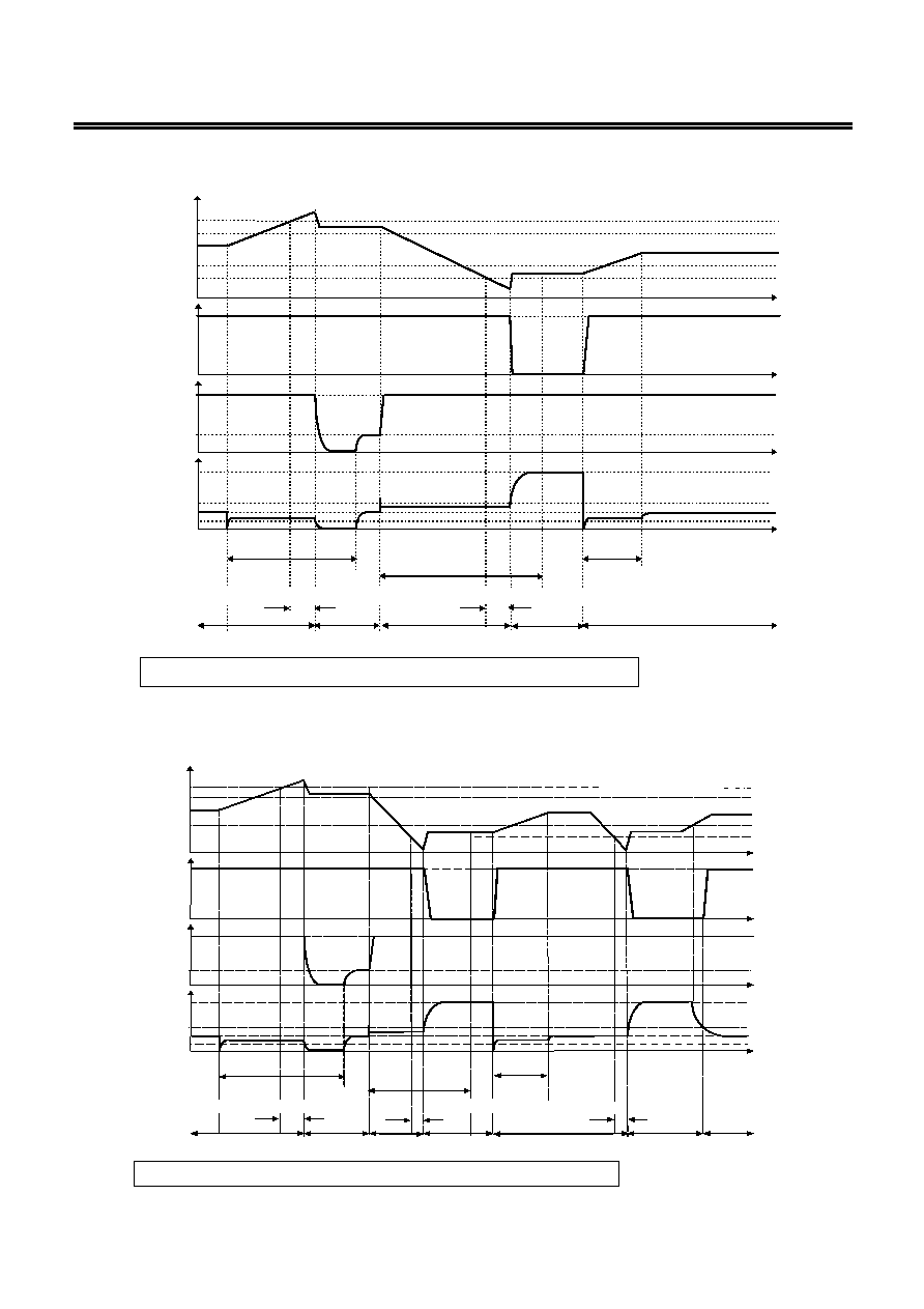
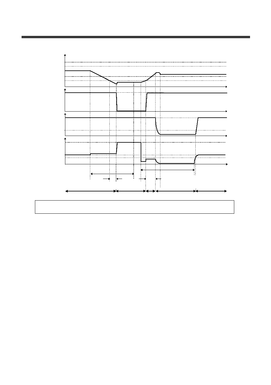
1-1. Overcharge and overdischarge detection (for products with power-down function)
V
C U
V
C L
V
D U
V
D L
V
D D
V
SS
V
D D
V
SS
V
D D
V
IOV 1
V
SS
V
C HA
Mode
Note: Normal mode,
Overcharge mode, Overdischarge mode, Overcurrent mode
The charger is assumed to charge with a constant current.
Battery
voltage
DO pin
CO pin
VM pin
C harger
connected
Load
connected
Overcharge detection delay tim e (t
CU
)
Overdischarge detection delay tim e (t
DL
)
Figure 6-1
1-2. Overcharge and overdischarge detection (for products without power-down function)
V
C U
V
C L
V
D U
V
D L
B a tte r y
v o lt a g e
D O p in
V
D D
V
S S
V
D D
V
S S
V
D D
V
IO V 1
V
S S
V
C H A
C O p in
V M p in
C h a rg e r
c o n n e c te d
O v e rc h a rg e d e te c tio n d e la y tim e (t
C U
)
O v e rd is c h a rg e d e te c tio n d e la y tim e (t
D L
)
O v e rd is c h a rg e d e te c tio n d e la y tim e (t
D L
)
L o a d
c o n n e c te d
M o d e
N o te :
N o rm a l m o d e ,
O v e rc h a rg e m o d e ,
O v e rd is c h a rg e m o d e ,
O v e rc u rre n t m o d e
T h e c h a rg e r is a s s u m e d to c h a rg e w ith a c o n s ta n t c u rre n t.
Figure 6-2

BATTERY PROTECTION IC FOR A SINGLE CELL PACK
Rev.3.8
_00
S-8241 Series
Seiko Instruments Inc.
19
2. Overcurrent detection
V
CU
V
CL
V
DU
V
DL
V
DD
V
SS
V
DD
V
SS
(1)
(4)
(1)
(4)
(1)
(4)
(1)
V
DD
V
IOV1
V
SS
V
SHORT
V
IOV2
Overcurrent 1 detection delay time (t
IOV1
)
Overcurrent 2 detection delay time (t
IOV2
) Load short-circuiting detection delay time (t
SHORT
)
Battery
voltage
DO pin
CO pin
VM pin
Charger connection
Load connection
Mode
Note: (1) Normal mode, (2) Overcharge mode, (3) Overdischarge mode, (4) Overcurrent mode
The charger is assumed to charge with constant current.
Figure 7
3. Charger detection
V
CU
V
CL
V
DU
V
DL
V
DD
V
SS
V
DD
V
SS
V
DD
V
SS
V
CHA
Overdischarge detection delay time (t
DL
)
If VM pin voltage
< V
CHA
Overdischarge is released at
overdischarge detection voltage (V
DL
)
(1)
(3)
(1)
Battery
voltage
DO pin
CO pin
VM pin
Charger connection
Load connection
Mode
Note: (1) Normal mode, (2) Overcharge mode, (3) Overdischarge mode, (4) Overcurrent mode
The charger is assumed to charge with constant current.
Figure 8
BATTERY PROTECTION IC FOR A SINGLE CELL PACK
S-8241 Series
Rev.3.8
_00
Seiko Instruments Inc.
20
4. Abnormal charge current detection
Abnormal charging current detection delay time
( = Overcharge detection delay time (t
CU
))
Overdischarge detection delay time (t
DL
)
(3)
(1)
(2)
(1)
(1)
Battery
voltage
DO pin
CO pin
VM pin
Charger connection
Load connection
Mode
Note: (1) Normal mode, (2) Overcharge mode, (3) Overdischarge mode, (4) Overcurrent mode
The charger is assumed to charge with constant current.
V
CU
V
CL
V
DU
V
DL
V
DD
V
SS
V
DD
V
SS
V
DD
V
SS
V
CHA
Figure 9
BATTERY PROTECTION IC FOR A SINGLE CELL PACK
Rev.3.8
_00
S-8241 Series
Seiko Instruments Inc.
21
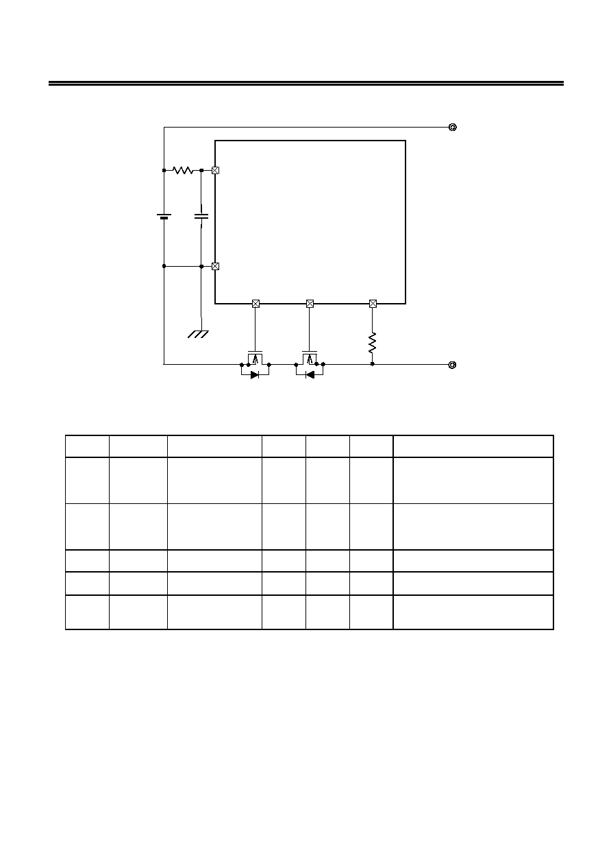
Battery Protection IC Connection Example
EB+
EB
-
S-8241 Series
470
VSS
Battery
DO
VDD
R2
C1
CO VM
FET1
FET2
R1
0.1
µF
1 k
Figure 10
Table 1 Constant
Symbol Parts
Purpose
Recomm
ended
min. max.
Remarks
FET1
Nch
MOS_FET
Charge control
0.4 V
Threshold voltage overdischarge
detection voltage.
*1
Withstand voltage between gate and
source
Charger voltage
*2
FET2
Nch
MOS_FET
Discharge control
0.4 V
Threshold voltage overdischarge
detection voltage.
*1
Withstand voltage between gate and
source
Charger voltage
*2
R1 Resistor
Protection for ESD and
power fluctuation
470
300
R2 value Relation R1
R2 should be maintained.
*3
C1 Capacitor
Protection for power
fluctuation
0.1
µF 0.01
µF 1.0
µF
Install a capacitor of 0.01
µF or
higher between VDD and VSS.
*4
R2 Resistor
Protection for charger
reverse connection
1 k
300
1.3
k
To suppress current flow caused by reverse
connection of a charger, set the resistance
within the range from 300
to 1.3 k.
*5
*1. If an FET with a threshold voltage of 0.4 V or lower is used, the FET may fail to cut the charging current.
If an FET with a threshold voltage equal to or higher than the overdischarge detection voltage is used, discharging may stop before
overdischarge is detected.
*2. If the withstand voltage between the gate and source is lower than the charger voltage, the FET may break.
*3. If R1 has a higher resistance than R2 and if a charger is connected reversely, current flows from the charger to the IC and the
voltage between VDD and VSS may exceed the absolute maximum rating. Install a resistor of 300
or higher as R1 for ESD
protection.
If R1 has a high resistance, the overcharge detection voltage increases by IC current consumption.
*4. If a capacitor C1 is less than 0.0 1
µF, DO may oscillate when load short-circuiting is detected, a charger is connected reversely, or
overcurrent 1 or 2 is detected.
A capacitor of 0.01
µF or higher as C1 should be installed. In some types of batteries DO oscillation may not stop unless the C1
capacity is increased. Set the C1 capacity by evaluating the actual application.
*5. If R2 is set to less than 300
, a current which is bigger than the power dissipation flows through the IC and the IC may break when
a charger is connected reversely. If a resistor bigger than 1.3 k
is installed as R2, the charging current may not be cut when a
high-voltage charger is connected.
Caution The above connection diagram and constant will not guarantee successful operation. Perform thorough evaluation
using the actual application to set the constant.

BATTERY PROTECTION IC FOR A SINGLE CELL PACK
S-8241 Series
Rev.3.8
_00
Seiko Instruments Inc.
22
Precautions
∑ Pay attention to the operating conditions for input/output voltage and load current so that the power loss
in the IC does not exceed the power dissipation of the package.
∑ Do not apply an electrostatic discharge to this IC that exceeds the performance ratings of the built-in
electrostatic protection circuit.
∑ Seiko Instruments Inc. shall not be responsible for any patent infringement by products including the
S-8241 series in connection with the method of using the S-8241 series in such products, the product
specifications or the country of destination thereof.
BATTERY PROTECTION IC FOR A SINGLE CELL PACK
Rev.3.8
_00
S-8241 Series
Seiko Instruments Inc.
23
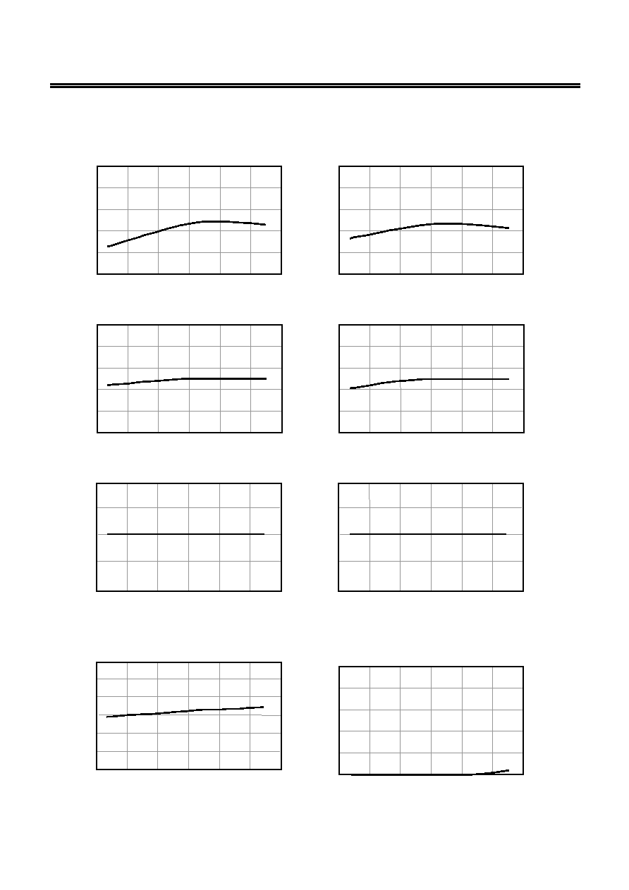
Characteristic (typical characteristic)
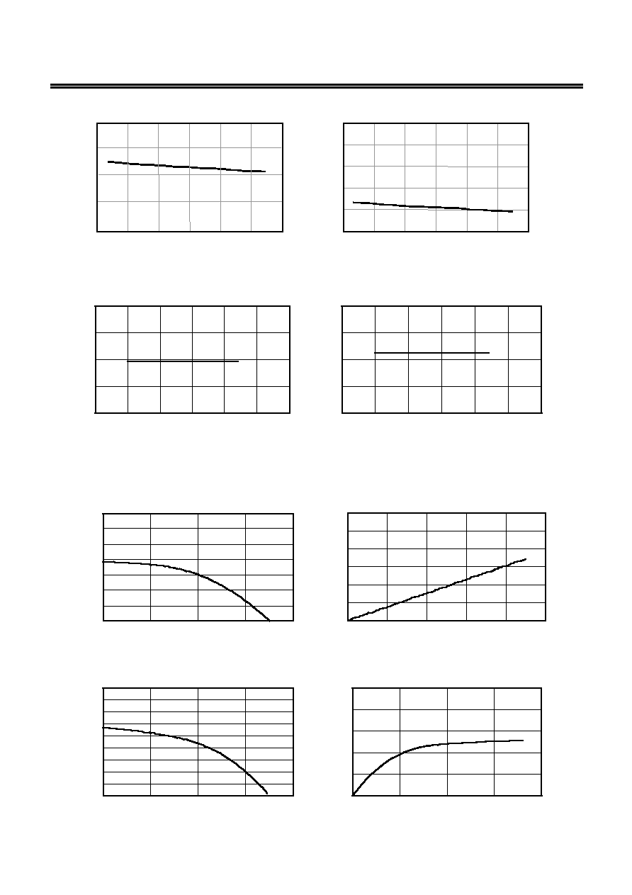
1. Detection/release voltage temperature characteristics
4.23
4.25
4.27
4.29
4.31
4.33
-50 -25 0 25 50 75 100
Ta(∞C)
V
CU
(V
)
Overcharge detection voltage vs. temperature
4.13
4.15
4.17
4.19
4.21
4.23
-50 -25 0 25 50 75 100
Ta(∞C)
V
CL
(V
)
Overcharge release voltage vs. temperature
2.20
2.24
2.28
2.32
2.36
2.40
-50 -25 0 25 50 75 100
Ta(∞C)
V
DL
(V
)
Overdischarge detection voltage vs. temperature
2.30
2.34
2.38
2.42
2.46
2.50
-50 -25 0 25 50 75 100
Ta(∞C)
V
DU
(V
)
Overdischarge release voltage vs. temperature
0.090
0.095
0.100
0.105
0.110
-50 -25 0 25 50 75 100
Ta(∞C)
V
IOV1
(V
)
Overcurrent 1 detection voltage vs. temperature
0.40
0.45
0.50
0.55
0.60
-50 -25 0 25 50 75 100
Ta(∞C)
V
IOV2
(V
)
Overcurrent 2 detection voltage vs. temperature
2. Current consumption temperature characteristics
0
1
2
3
4
5
6
-25 0 25 50 75
Ta(∞C)
I
OPE
(
µ
A)
Current consumption vs. Temperature in normal mode
-50 100
0.00
0.02
0.04
0.06
0.08
0.10
-50 -25 0 25 50 75 100
Ta(∞C)
I
PDN
(
µ
A)
Current consumption vs. Temperature in power-down mode
BATTERY PROTECTION IC FOR A SINGLE CELL PACK
S-8241 Series
Rev.3.8
_00
Seiko Instruments Inc.
24
3. Current comsumption Power voltage characteristics (Ta=25∞C)
Current consumption - -
power supply volatge dependency
0
5
10
15
20
0 2 4 6 8 10
V
DD
(V)
I
OPE
(
µA)
V
M
=V
SS
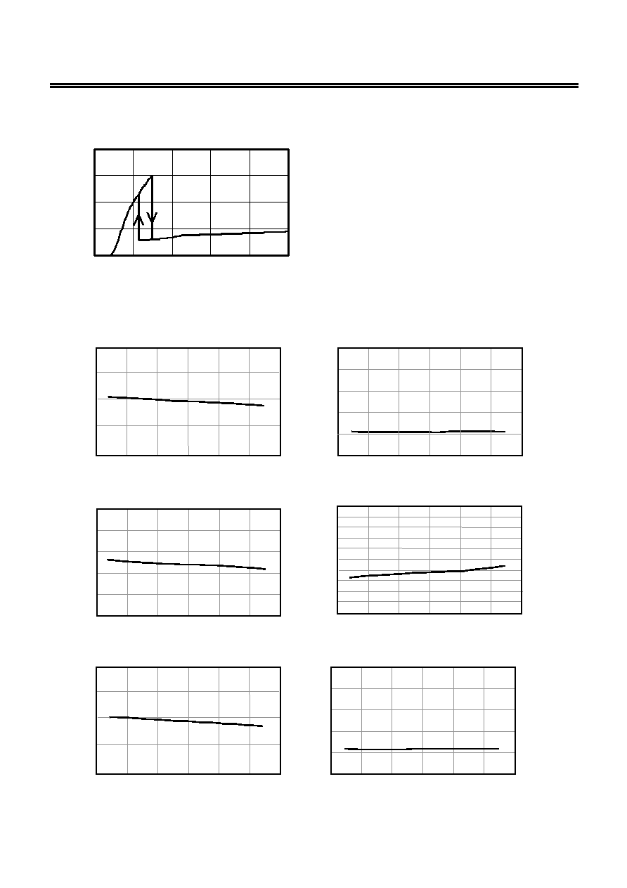
4. Detection/release delay time temperature characteristics
0.0
0.5
1.0
1.5
2.0
-50 -25 0 25 50 75 100
Ta(∞C)
t
cu
(s)
Overcharge detection delay time vs. temperature
0.0
0.2
0.4
0.6
0.8
1.0
-50 -25 0 25 50 75 100
Ta(∞C)
t
CL
(m
s)
Overcharge release delay time vs. temperature
0
50
100
150
200
250
-50 -25 0 25 50
100
Ta(∞C)
t
DL
(m
s)
Overdischarge detection delay time vs. temperature
75
0.0
0.2
0.4
0.6
0.8
1.0
1.2
1.4
1.6
1.8
2.0
-50 -25 0 25 50 75 100
Ta(∞C)
t
cu
(s)
Overdischarge release delay time vs. temperature
0
4
8
12
16
-50 -25 0 25 50 75 100
Ta(∞C)
t
IOV1
(m
s)
Overcurrent 1 detection delay time vs. temperature
0
100
200
300
400
500
-50
-25 0 25 50 75 100
Ta(∞C)
t
IOV1
(
µ
s
)
Releas
e
Overcurrent 1 release delay time vs. temperature
BATTERY PROTECTION IC FOR A SINGLE CELL PACK
Rev.3.8
_00
S-8241 Series
Seiko Instruments Inc.
25
0
1
2
3
4
-50 -25 0 25 50 75 100
Ta(∞C)
t
IOV2
(m
s)2
Overcurrent 2 detection delay time vs. temperature
0
10
20
30
40
50
-50 -25 0 25 50 75 100
Ta(∞C)
t
SHORT
(
µ
s)
Load short-circuiting delay time vs. temperature
5. Delay time power-voltage characteristics(Ta=25∞C)
Overcurrent 1 detection delay time vs. power supply
voltage dependency
0
4
8
12
16
2.0
2.5
3.0
3.5
4.0
4.5
5.0
V
DD
(V)
t
IOV1
(ms)
Overcurrent 2 detection delay time vs. power supply
voltage dependency
0
1
2
3
4
2.0
2.5
3.0
3.5
4.0
4.5
5.0
V
DD
(V)
t
IOV2
(ms)
6. CO pin/DO pin output current characteristics(Ta=25∞C)
CO pin source current characteristics
-1.4
-1.2
-1.0
-0.8
-0.6
-0.4
-0.2
0.0
0
1
2
3
4
V
CO
(V)
I
CO
(mA)
V
DD
=3.5V,V
SS
=V
M
=0V
CO pin sink current characteristics
0
2
4
6
8
10
12
0
1
2
3
4
5
V
CO
(V)
I
CO
(
µA)
V
DD
=4.5V,V
SS
=V
M
=0V
DO pin source current characteristics
-1.8
-1.6
-1.4
-1.2
-1.0
-0.8
-0.6
-0.4
-0.2
0.0
0
1
2
3
4
V
DO
(V)
I
DO
(mA)
V
DD
=3.5V,V
SS
=V
M
=0V
DO pin sink current characteristics
0.0
0.5
1.0
1.5
2.0
2.5
0.0
0.5
1.0
1.5
2.0
V
DO
(V)
I
DO
(mA)
V
DD
=1.8V,V
SS
=V
M
=0V
No.
TITLE
SCALE
UNIT
mm
Seiko Instruments Inc.
2.9±0.2
1.9±0.2
0.95±0.1
0.4±0.1
0.16
+0.1
-0.06
1
2
3
4
5
No. MP005-A-P-SD-1.2
MP005-A-P-SD-1.2
SOT235-A-PKG Dimensions
No.
TITLE
SCALE
UNIT
mm
Seiko Instruments Inc.
¯1.5
+0.1
-0
2.0±0.05
¯1.0
+0.2
-0
4.0±0.1
1.4±0.2
0.25±0.1
3.2±0.2
1
2
3
4
5
No. MP005-A-C-SD-2.1
MP005-A-C-SD-2.1
SOT235-A-Carrier Tape
Feed direction
4.0±0.1(10 pitches:40.0±0.2)
No.
TITLE
SCALE
UNIT
mm
Seiko Instruments Inc.
12.5max.
9.0±0.3
¯13±0.2
(60∞)
(60∞)
QTY.
3,000
No. MP005-A-R-SD-1.1
MP005-A-R-SD-1.1
SOT235-A-Reel
Enlarged drawing in the central part
2.0±0.2
1
5
0.2
0.65
No.
TITLE
SCALE
UNIT
mm
4
2
3
+0.1
-0.05
0.65
1.3±0.1
No. PN005-A-P-SD-1.1
PN005-A-P-SD-1.1
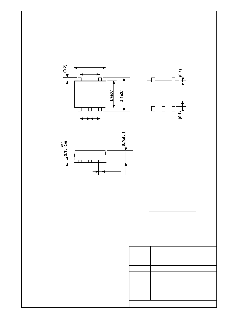
SON5A-A-PKG Dimensions
Seiko Instruments Inc.
¯1.55±0.05
¯1.05±0.1
4.0±0.1
4.0±0.1
0.2±0.05
1.1±0.1
2.05±0.1
(2.25)
No.
TITLE
SCALE
UNIT
mm
1
2
5
4
3
2.0±0.1
No. PN005-A-C-SD-1.1
PN005-A-C-SD-1.1
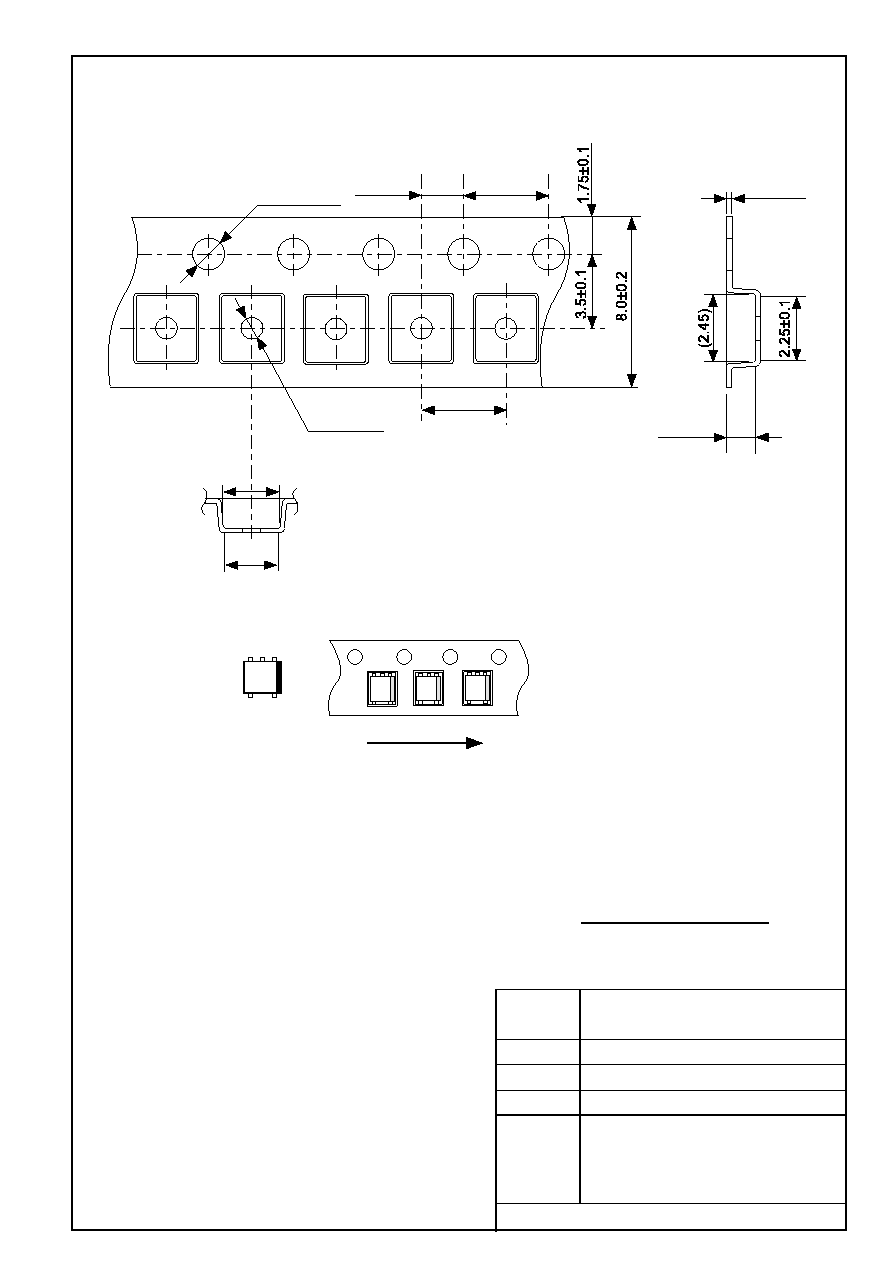
SON5A-A-Carrier Tape
Feed direction
Seiko Instruments Inc.
No.
TITLE
SCALE
UNIT
mm
QTY.
3000
12.5max.
9.0±0.3
Seiko Instruments Inc.
Enlarged drawing in the central part
No. PN005-A-R-SD-1.1
PN005-A-R-SD-1.1
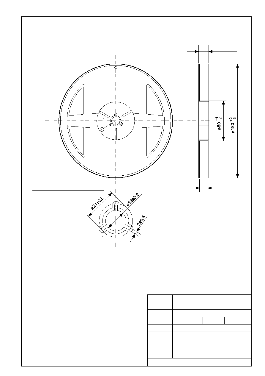
SON5A-A-Reel

∑
The information described herein is subject to change without notice.
∑
Seiko Instruments Inc. is not responsible for any problems caused by circuits or diagrams described herein
whose related industrial properties, patents, or other rights belong to third parties. The application circuit
examples explain typical applications of the products, and do not guarantee the success of any specific
mass-production design.
∑
When the products described herein are regulated products subject to the Wassenaar Arrangement or other
agreements, they may not be exported without authorization from the appropriate governmental authority.
∑
Use of the information described herein for other purposes and/or reproduction or copying without the
express permission of Seiko Instruments Inc. is strictly prohibited.
∑
The products described herein cannot be used as part of any device or equipment affecting the human
body, such as exercise equipment, medical equipment, security systems, gas equipment, or any apparatus
installed in airplanes and other vehicles, without prior written permission of Seiko Instruments Inc.
∑
Although Seiko Instruments Inc. exerts the greatest possible effort to ensure high quality and reliability, the
failure or malfunction of semiconductor products may occur. The user of these products should therefore
give thorough consideration to safety design, including redundancy, fire-prevention measures, and
malfunction prevention, to prevent any accidents, fires, or community damage that may ensue.