 | –≠–Ľ–Ķ–ļ—ā—Ä–ĺ–Ĺ–Ĺ—č–Ļ –ļ–ĺ–ľ–Ņ–ĺ–Ĺ–Ķ–Ĺ—ā: S-8242 | –°–ļ–į—á–į—ā—Ć:  PDF PDF  ZIP ZIP |
Document Outline
- S-8242 Series
- COVER
- Features
- Applications
- Package
- Block Diagram
- Product Code Structure
- Pin Assignment
- Absolute Maximum Ratings
- Electrical Characteristics
- Test Circuits
- Description of Operation
- Operation Timing Chart
- Standard Circuit
- Precautions
- Characteristics (Typical Data)
- Package Drawing

Rev.1.0
_00
BATTERY PROTECTION IC
FOR 2-SERIAL-CELL PACK
S-8242 Series
Seiko Instruments Inc.
1
The S-8242 Series are protection ICs for 2-serial-cell
lithium-ion/lithium-polymer rechargeable batteries and include
high-accuracy voltage detectors and delay circuits.
These ICs are suitable for protecting 2-cell rechargeable
lithium-ion/lithium-polymer battery packs from overcharge,
overdischarge, and overcurrent.
Features
(1) High-accuracy voltage detection for each cell
∑ Overcharge detection voltage n (n = 1, 2)
3.9 V to 4.4 V (50 mV steps) Accuracy
Ī25 mV
∑ Overcharge release voltage n (n = 1, 2)
3.8 V to 4.4 V
*1
Accuracy
Ī50 mV
*1. Overcharge release voltage
= Overcharge detection voltage - Overcharge hysteresis voltage
(Overcharge hysteresis voltage n (n
= 1, 2) can be selected as 0 V or from a range of 0.1 V to
0.4 V in 50 mV steps.)
∑ Overdischarge detection voltage n (n = 1, 2)
2.0 V to 3.0 V (100 mV steps) Accuracy
Ī50 mV
∑ Overdischarge release voltage n (n = 1, 2)
2.0 V to 3.4 V
*2
Accuracy
Ī100 mV
*2. Overdischarge release voltage
= Overdischarge detection voltage + Overdischarge hysteresis
voltage
(Overdischarge hysteresis voltage n (n
= 1, 2) can be selected as 0 V or from a range of 0.1 V to
0.7 V in 100 mV steps.)
(2) Two-level overcurrent detection (overcurrent 1, overcurrent 2)
∑ Overcurrent detection voltage 1
0.05 V to 0.30 V (50 mV steps) Accuracy
Ī15 mV
∑ Overcurrent detection voltage 2
1.2 V (fixed)
Accuracy
Ī300 mV
(3) Delay times (overcharge, overdischarge, overcurrent) are generated by an internal circuit (external
capacitors are unnecessary).
(4) 0 V battery charge function available/unavailable are selectable.
(5) Charger detection function and abnormal charge current detection function
∑ The overdischarge hysteresis is released by detecting negative voltage at the VM pin (-0.7 V typ.).
(Charger detection function)
∑ When the output voltage of the DO pin is high and the voltage at the VM pin is equal to or lower than
the charger detection voltage (
-0.7 V typ.), the output voltage of the CO pin goes low. (Abnormal
charge current detection function)
(6) High-withstanding-voltage devices
Absolute maximum rating: 28 V
(7) Wide operating temperature range
-40įC to +85 įC
(8) Low current consumption
∑ Operation mode
10
ĶA max. (+25įC)
∑ Power-down mode
0.1
ĶA max. (+25įC)
(9) Small package
SOT-23-6W, 6-Pin SNB(B)
Applications
∑ Lithium-ion rechargeable battery packs
∑ Lithium-polymer rechargeable battery packs
Package
∑ SOT-23-6W (PKG drawing code: MP006-B)
∑ 6-Pin SNB(B) (PKG drawing code: BD006-A)

BATTERY PROTECTION IC FOR 2-SERIAL-CELL PACK
S-8242 Series
Rev.1.0
_00
Seiko Instruments Inc.
2
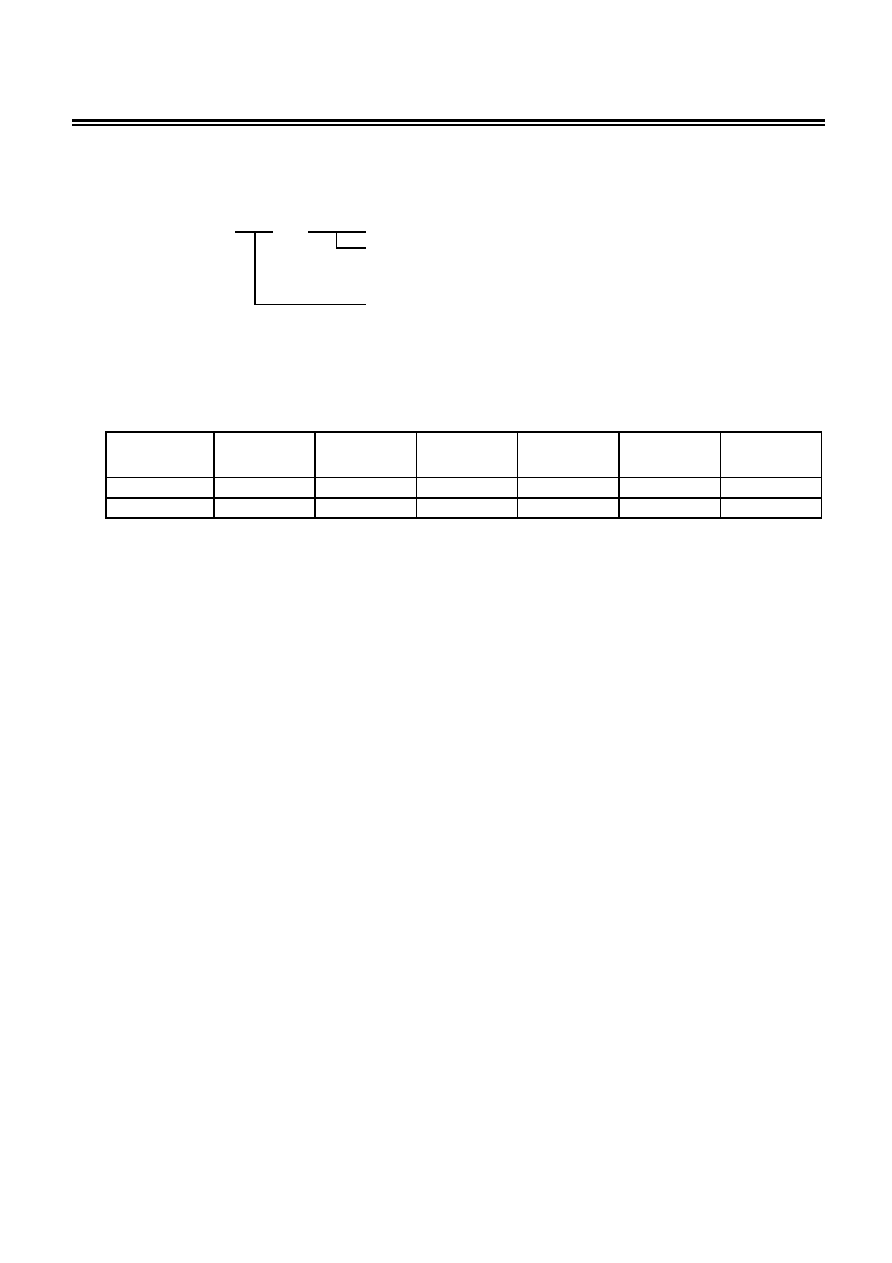
Block Diagram
CO
VDD
DO
VM
300 k
20 k
+
-
+
-
Delay circuit, controller,
0 V battery charge/
charge inhibition circuit
VC
-
+
+
-
-
+
+
-
VSS
Charger
detector
Remark The diodes in the block diagram are parasitic diodes.
Figure 1 Block Diagram
BATTERY PROTECTION IC FOR 2-SERIAL-CELL PACK
Rev.1.0
_00
S-8242 Series
Seiko Instruments Inc.
3
Product Name Structure
1. Product Name
S
-
-
-
-8242A xx ---- XXXX
Indicates package type and packing specification of IC
*1
M6T2: SOT-23-6W, tape product
B6T1: 6-pin SNB(B), tape product
Additional number
Sequentially set from AA to ZZ
*1. Refer to the taping drawing.
2. Product Name List
Table 1
Product
Name/Parameter
Overcharge
Detection Voltage
V
CU
Overcharge
Release Voltage
V
CL
Overdischarge
Detection Voltage
V
DL
Overdischarge
Release Voltage
V
DU
Overcurrent
Detection Voltage 1
V
IOV1
0 V Battery
Charge
S-8242AAA-M6T2
4.325 V
4.075 V
2.200 V
2.900 V
0.210 V
Unavailable
S-8242AAA-B6T1
4.325 V
4.075 V
2.200 V
2.900 V
0.210 V
Unavailable
Remark If a product with the required detection voltage does not appear in the above list, contact our sales
office.

BATTERY PROTECTION IC FOR 2-SERIAL-CELL PACK
S-8242 Series
Rev.1.0
_00
Seiko Instruments Inc.
4
Pin Assignment
SOT-23-6W
Top view
Table 2
Pin No.
Pin
Name
Function
1 DO
Connection of discharge control FET gate
(CMOS output)
2 CO
Connection of charge control FET gate (CMOS
output)
3 VM
Voltage detection between VM and VSS
(overcurrent/charger detection pin)
4 VC
Connection for negative voltage of battery 1 and
positive voltage of battery 2
5 VDD
Connection for positive power supply input and
positive voltage of battery 1
6 VSS
Connection for negative power supply input and
negative voltage of battery 2
4
5
6
1
3
2
Figure 2
Remark For the external views, refer to the package drawings.
6-Pin SNB(B)
Top view
Table 3
Pin No.
Pin
Name
Function
1 VM
Voltage detection between VM and VSS
(overcurrent/charger detection pin)
2 CO
Connection of charge control FET gate (CMOS
output)
3 DO
Connection of discharge control FET gate
(CMOS output)
4 VSS
Connection for negative power supply input and
negative voltage of battery 2
5 VC
Connection for negative voltage of battery 1 and
positive voltage of battery 2
6 VDD
Connection for positive power supply input and
positive voltage of battery 1
1
4
6
5
3
2
Figure 3
Remark For the external views, refer to the package drawings.
BATTERY PROTECTION IC FOR 2-SERIAL-CELL PACK
Rev.1.0
_00
S-8242 Series
Seiko Instruments Inc.
5
Absolute Maximum Ratings
Table 4
(Ta
= 25įC unless otherwise specified)
Parameter
Symbol
Applicable Pins
Absolute Maximum Rating Unit
Input voltage between VDD and VSS
*1
V
DS
VDD
V
SS
- 0.3 to V
SS
+ 12
V
VC input pin voltage
V
VC
VC
V
SS
- 0.3 to V
DD
+ 0.3
VM pin input voltage
V
VM
VM
V
DD
- 28 to V
DD
+ 0.3
DO pin output voltage
V
DO
DO
V
SS
- 0.3 to V
DD
+ 0.3
CO pin output voltage
V
CO
CO
V
VM
- 0.3 to V
DD
+ 0.3
SOT-23-6W 300
Power dissipation
P
D
6-Pin SNB(B)
90
mW
Operating temperature range
T
opr
-40 to +85
įC
Storage temperature range
T
stg
-55 to +125
*1. Even pulse (
Ķs) noise exceeding the above input voltage (V
SS
+ 12 V) may damage the IC, so do not
allow such noise to be applied.
Caution The absolute maximum ratings are rated values exceeding which the product could
suffer physical damage. These values must therefore not be exceeded under any
conditions.

BATTERY PROTECTION IC FOR 2-SERIAL-CELL PACK
S-8242 Series
Rev.1.0
_00
Seiko Instruments Inc.
6
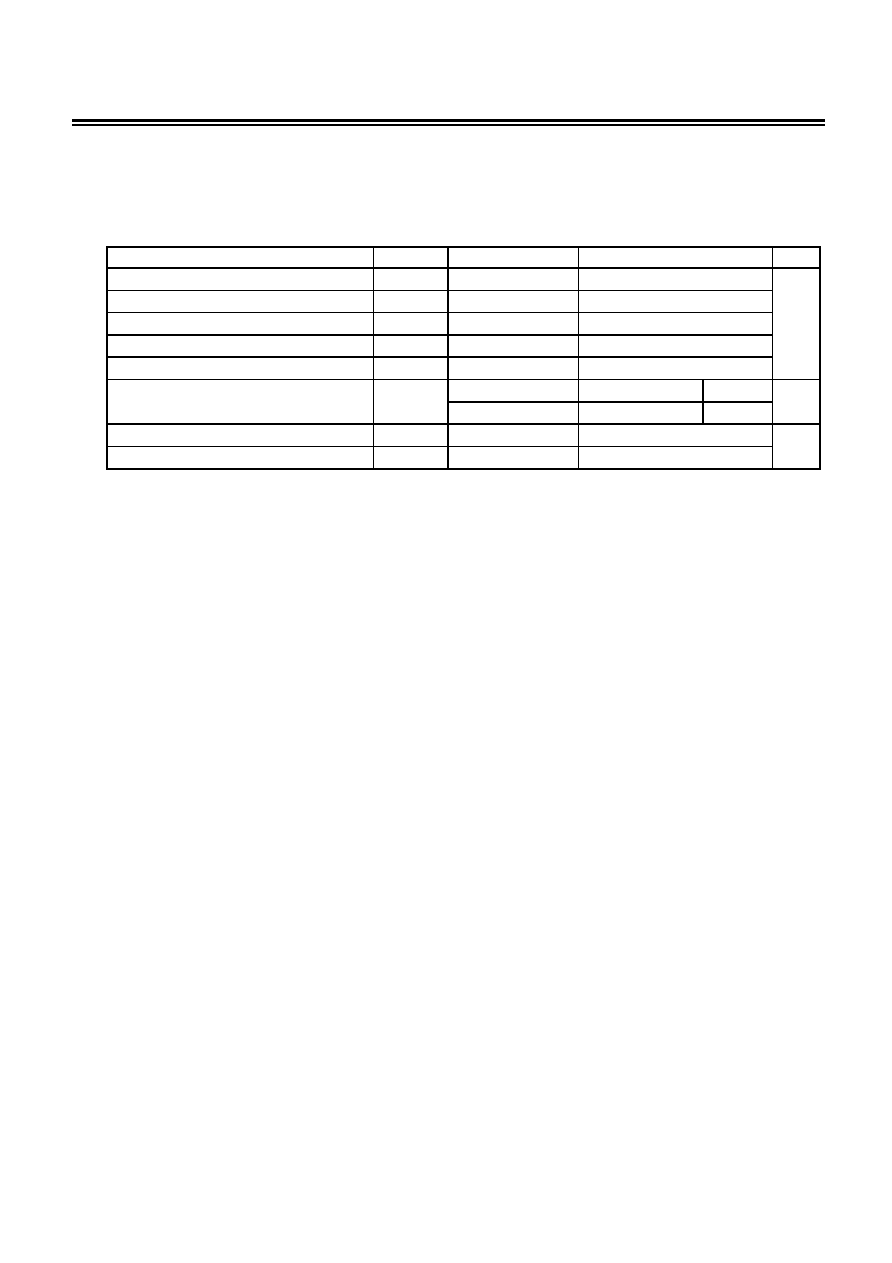
Electrical Characteristics
Table 5
(Ta
= 25įC unless otherwise specified)
Parameter Symbol
Conditions
Min.
Typ.
Max.
Unit
Test
Conditions
Test
Circuit
DETECTION VOLTAGE
Overcharge detection voltage n
V
CUn
3.90 to 4.40 V, adjustable
V
CUn
- 0.025
V
CUn
V
CUn
+ 0.025
V 1 1
Overcharge release voltage n
V
CLn
3.80 to 4.40 V, adjustable
V
CLn
- 0.05
V
CLn
V
CLn
+ 0.05
V 1 1
Overdischarge detection voltage n
V
DLn
2.0 to 3.0 V, adjustable
V
DLn
- 0.05
V
DLn
V
DLn
+ 0.05
V 2 1
Overdischarge release voltage n
V
DUn
2.0 to 3.40 V, adjustable
V
DUn
- 0.10
V
DUn
V
DUn
+ 0.10
V 2 1
Overcurrent detection voltage 1
V
IOV1
0.05 to 0.3 V, adjustable
V
IOV1
-
0.015
V
IOV1
V
IOV1
+
0.015
V 3 1
Overcurrent detection voltage 2
V
IOV2
0.9 1.2 1.5
V
3
1
Charger detection voltage
V
CHA
-1.0
-0.7
-0.4
V 4 1
Temperature coefficient 1
T
COE1
Ta
= 0 to 50įC
*1
-1.0
0 1.0
mV/
įC
Temperature coefficient 2
T
COE2
Ta
= 0 to 50įC
*2
-0.5
0 0.5
mV/
įC
DELAY TIME
Overcharge detection delay time
t
CU
0.92 1.15 1.38
s
9
1
Overdischarge detection delay time
t
DL
115 144 173
ms
9
1
Overcurrent detection delay time 1
t
IOV1
7.2 9 11
ms
10
1
Overcurrent detection delay time 2
t
IOV2
FET gate capacitance
= 2000 pF
220 300 380
Ķs
10 1
0 V BATTERY CHARGE FUNCTION
0 V charge starting charger voltage
V
0CHA
0 V charge available
1.2
V
11 1
0 V battery charge inhibition battery
voltage
V
0INH
0 V charge unavailable
0.5 V
12 1
INTERNAL RESISTANCE
Resistance between VM and VDD
R
VMD
V1
= V2 = 1.5 V
V
VM
= 0 V
100 300 900
k
6 2
Resistance between VM and VSS
R
VMS
V1
= V2 = 3.5 V
V
VM
= 1.0 V
5 10 20
k
6 2
INPUT VOLTAGE
Operating voltage between VDD
and VSS
V
DSOP1
Internal circuit operating
voltage
1.5
10 V
-
-
Operating voltage between VDD
and VM
V
DSOP2
Internal circuit operating
voltage
1.5
28 V
-
-
INPUT CURRENT
Current consumption during
operation
I
OPE
V1
= V2 = 3.5 V,
V
VM
= 0 V
5 10
ĶA 5 2
Current consumption at power
down
I
PDN
V1
= V2 = 1.5 V,
V
VM
= 3.0 V
0.1
ĶA 5 2
VC pin current
I
VC
V1
= V2 = 3.5 V,
V
VM
= 0 V
-0.3
0 0.3
ĶA 5 2
OUTPUT RESISTANCE
CO pin H resistance
R
COH
V
CO
= V
DD
- 0.5 V
2 4 8
k
7 3
CO pin L resistance
R
COL
V
CO
= V
VM
+ 0.5 V
2 4 8
k
7 3
DO pin H resistance
R
DOH
V
DO
= V
DD
- 0.5 V
2 4 8
k
8 3
DO pin L resistance
R
DOL
V
DO
= V
SS
+ 0.5 V
2 4 8
k
8 3
*1. Voltage temperature coefficient 1: Overcharge detection voltage
*2. Voltage temperature coefficient 2: Overcurrent detection voltage 1

BATTERY PROTECTION IC FOR 2-SERIAL-CELL PACK
Rev.1.0
_00
S-8242 Series
Seiko Instruments Inc.
7
Test Circuits
Remark Unless otherwise specified, the output voltage levels "H" and "L" at CO and DO pins are judged by the
threshold voltage (1.0 V) of the N-channel FET. Judge the CO pin level with respect to V
VM
and the
DO pin level with respect to V
SS
.
1. Overcharge detection voltage, overcharge release voltage
(Test Condition 1, Test Circuit 1)
Overcharge detection voltage 1 (V
CU1
) is defined as the voltage between the VDD and VC pins at which V
CO
goes from "H" to "L" when the voltage V1 is gradually increased from the starting condition of V1
= V2 = 3.5
V, V3
= 0 V. Overcharge release voltage 1 (V
CL1
) is defined as the voltage between the VDD and VC pins at
which V
CO
goes from "L" to "H" when the voltage V1 is then gradually decreased. Overcharge hysteresis
voltage 1 (V
HC1
) is defined as the difference between overcharge detection voltage 1 (V
CU1
) and overcharge
release voltage 1 (V
CL1
).
Overcharge detection voltage 2 (V
CU2
) is defined as the voltage between the VC and VSS pins at which V
CO
goes from "H" to "L" when the voltage V2 is gradually increased from the starting condition of V1
= V2 = 3.5
V, V3
= 0 V. Overcharge release voltage 2 (V
CL2
) is defined as the voltage between the VC and VSS pins at
which V
CO
goes from "L" to "H" when the voltage V2 is then gradually decreased. Overcharge hysteresis
voltage 2 (V
HC2
) is defined as the difference between overcharge detection voltage 2 (V
CU2
) and overcharge
release voltage 2 (V
CL2
).
2. Overdischarge detection voltage, overdischarge release voltage
(Test Condition 2, Test Circuit 1)
Overdischarge detection voltage 1 (V
DL1
) is defined as the voltage between the VDD and VC pins at which
V
DO
goes from "H" to "L" when the voltage V1 is gradually decreased from the starting condition of V1
= V2
= 3.5 V, V3 = 0 V. Overdischarge release voltage 1 (V
DU1
) is defined as the voltage between the VDD and
VC pins at which V
DO
goes from "L" to "H" when the voltage V1 is then gradually increased. Overdischarge
hysteresis voltage 1 (V
HD1
) is defined as the difference between overdischarge release voltage 1 (V
DU1
) and
overdischarge detection voltage 1 (V
DL1
).
Overdischarge detection voltage 2 (V
DL2
) is defined as the voltage between the VC and VSS pins at which
V
DO
goes from "H" to "L" when the voltage V2 is gradually decreased from the starting condition of V1
= V2
= 3.5 V, V3 = 0 V. Overdischarge release voltage 2 (V
DU2
) is defined as the voltage between the VC and
VSS pins at which V
DO
goes from "L" to "H" when the voltage V2 is then gradually increased. Overdischarge
hysteresis voltage 2 (V
HD2
) is defined as the difference between overdischarge release voltage 2 (V
DU2
) and
overdischarge detection voltage 2 (V
DL2
).
3. Overcurrent detection voltage 1, overcurrent detection voltage 2
(Test Condition 3, Test Circuit 1)
Overcurrent detection voltage 1 (V
IOV1
) is defined as the voltage between the VM and VSS pins whose delay
time for changing V
DO
from "H" to "L" lies between the minimum and the maximum value of overcurrent
delay time 1 when the voltage V3 is increased rapidly within 10
Ķs from the starting condition of V1 = V2 =
3.5V, V3
= 0 V.
Overcurrent detection voltage 2 (V
IOV2
) is defined as the voltage between the VM and VSS pins whose delay
time for changing V
DO
from "H" to "L" lies between the minimum and the maximum value of overcurrent
delay time 2 when the voltage V3 is increased rapidly within 10
Ķs from the starting condition of V1 = V2 =
3.5V, V3
= 0 V.

BATTERY PROTECTION IC FOR 2-SERIAL-CELL PACK
S-8242 Series
Rev.1.0
_00
Seiko Instruments Inc.
8
4. Charger detection voltage (abnormal charge current detection voltage)
(Test Condition 4, Test Circuit 1)
The charger detection voltage (V
CHA
) is defined as the voltage between the VM and VSS pins at which V
DO
goes from "L" to "H" when the voltage V3 is gradually decreased from 0 V after the voltage V1 is gradually
increased from the starting condition of V1
= 1.8 V, V2 = 3.5 V, V3 = 0 V until the voltage V1 becomes V
DL1
+ (V
HD1
/2).
The charger detection voltage can be measured only in a product whose overdischarge hysteresis V
HD
0 V.
The abnormal charge current detection voltage is defined as the voltage between the VM and VSS pins at
which V
CO
goes from "H" to "L" when the voltage V3 is gradually decreased from the starting condition of V1
= V2 = 3.5 V, V3 = 0 V. The value of the abnormal charge current detection voltage is the same as that of
the charger detection voltage (V
CHA
).
5. Operating current consumption, power-down current consumption, VC pin current
(Test Condition 5, Test Circuit 2)
The operating current consumption (I
OPE
) is the current I
SS
that flows through the VSS pin and the VC pin
current (I
VC
) is the current I
C
that flows through the VC pin under the set conditions of V1
= V2 = 3.5 V and
S1:OFF, S2:ON (normal status).
The power-down current consumption (I
PDN
) is the current I
SS
that flows through the VSS pin under the set
conditions of V1
= V2 = 1.5 V and S1:ON, S2:OFF (overdischarge status).
6. Resistance between VM and VDD, resistance between VM and VSS
(Test Condition 6, Test Circuit 2)
The resistance between VM and VDD (R
VMD
) is the resistance between VM and VDD under the set
conditions of V1
= V2 = 1.5 V and S1:OFF, S2:ON.
The resistance between VM and VSS (R
VMS
) is the resistance between VM and VSS under the set
conditions of V1
= V2 = 3.5 V and S1:ON, S2:OFF.
7. CO pin H resistance, CO pin L resistance
(Test Condition 7, Test Circuit 3)
The CO pin H resistance (R
COH
) is the resistance at the CO pin under the set conditions of V1
= V2 = 3.5 V, V4
= 6.5 V.
The CO pin L resistance (R
COL
) is the resistance at the CO pin under the set conditions of V1
= V2 = 4.5 V, V4
= 0.5 V.
8. DO pin H resistance, DO pin L resistance
(Test Condition 8, Test Circuit 3)
The DO pin H resistance (R
DOH
) is the resistance at the DO pin under the set conditions of V1
= V2 = 3.5 V, V5
= 6.5 V.
The DO pin L resistance (R
DOL
) is the resistance at the DO pin under the set conditions of V1
= V2 = 4.5 V, V5
= 0.5 V.
9. Overcharge detection delay time, overdischarge detection delay time
(Test Condition 9, Test Circuit 1)
The overcharge detection delay time (t
CU
) is the time needed for V
CO
to change from "H" to "L" just after the
voltage V1 momentarily increases within 10
Ķs from overcharge detection voltage 1 (V
CU1
)
- 0.2 V to
overcharge detection voltage 1 (V
CU1
)
+ 0.2 V under the set conditions of V1 = V2 = 3.5 V, V3 = 0 V.
The overdischarge detection delay time (t
DL
) is the time needed for V
DO
to change from "H" to "L" just after
the voltage V1 momentarily decreases within 10
Ķs from overcharge detection voltage 1 (V
DL1
)
+ 0.2 V to
overcharge detection voltage 1 (V
DL1
)
- 0.2 V under the set condition of V1 = V2 = 3.5 V, V3 = 0 V.

BATTERY PROTECTION IC FOR 2-SERIAL-CELL PACK
Rev.1.0
_00
S-8242 Series
Seiko Instruments Inc.
9
10. Overcurrent detection delay time 1, overcurrent detection delay time 2
(Test Condition 10, Test Circuit 1)
Overcurrent detection delay time 1 (t
IOV1
) is the time needed for V
DO
to go to "L" after the voltage V3
momentarily increases within 10
Ķs from 0 V to 0.35 V under the set conditions of V1 = V2 = 3.5 V, V3 = 0 V.
Overcurrent detection delay time 2 (t
IOV2
) is the time needed for V
DO
to go to "L" after the voltage V3
momentarily increases within 10
Ķs from 0 V to 2.0 V under the set conditions of V1 = V2 = 3.5 V, V3 = 0 V.
11. 0 V charge starting charger voltage (products in which 0 V charge is available)
(Test Condition 11, Test Circuit 1)
The 0 V charge starting charger voltage (V
0CHA
) is defined as the voltage between the VDD and VM pins at
which V
CO
goes to "H" (V
VM
+ 0.1 V or higher) when the voltage V3 is gradually decreased from the starting
condition of V1
= V2 = V3 = 0 V.
12. 0 V charge inhibition battery voltage (products in which 0 V charge is unavailable)
(Test Condition 12, Test Circuit 1)
The 0 V charge inhibition charger voltage (V
0INH
) is defined as the voltage between the VDD and VSS pins at
which V
CO
goes to "H" (V
VM
+ 0.1 V or higher) when the voltages V1 and V2 are gradually increased from the
starting condition of V1
= V2 = 0 V, V3 = -4 V.

BATTERY PROTECTION IC FOR 2-SERIAL-CELL PACK
S-8242 Series
Rev.1.0
_00
Seiko Instruments Inc.
10
CO
VM
VDD
VC
VSS
DO
S-8242 Series
A
A
V
V3
V
V1
V2
Test Circuit 1
CO
VM
VDD
VC
VSS
DO
S-8242 Series
A
S1
S2
A
A
V2
V1
Test Circuit 2
CO
VM
VDD
VC
VSS
DO
S-8242 Series
A
A
A
V4
V1
V2
A
V5
Test Circuit 3
Figure 4

BATTERY PROTECTION IC FOR 2-SERIAL-CELL PACK
Rev.1.0
_00
S-8242 Series
Seiko Instruments Inc.
11
Description of Operation
Remark Refer to Standard Circuit.
1.
Normal status
This IC monitors the voltage of the battery connected between the VDD and VSS pins and the voltage
difference between the VM and VSS pins to control charging and discharging. When the battery voltage is
in the range from overdischarge detection voltage n (V
DLn
) to overcharge detection voltage n (V
CUn
), and the
VM pin voltage is in the range from the charger detection voltage (V
CHA
) to overcurrent detection voltage 1
(V
IOV1
), the IC turns both the charging and discharging control FETs on. This condition is called the normal
status, and in this condition charging and discharging can be carried out freely.
Caution When the battery is connected for the first time, discharging may not be enabled. In this
case, short the VM and VSS pins or connect the charger to restore the normal status.
2.
Overcharge status
When the battery voltage becomes higher than overcharge detection voltage n (V
CUn
) during charging in the
normal status and detection continues for the overcharge detection delay time (t
CU
) or longer, the S-8242
Series turns the charging control FET off to stop charging. This condition is called the overcharge status.
The overcharge status is released in the following two cases (a and b).
a) When the battery voltage falls below overcharge release voltage n (V
CLn
), the S-8242 Series turns the
charging control FET on and returns to the normal status.
b) When a load is connected and discharging starts, the S-8242 Series turns the charging control FET
on and returns to the normal status. Just after the load is connected and discharging starts, the
discharging current flows through the parasitic diode in the charging control FET. At this moment the
VM pin potential becomes V
f
, the voltage for the parasitic diode, higher than the V
SS
level. When the
battery voltage goes under overcharge detection voltage n (V
CUn
) and provided that the VM pin
voltage is higher than overcurrent detection voltage 1, the S-8242 Series releases the overcharge
condition.
Cautions 1. If the battery is charged to a voltage higher than overcharge detection voltage n
(V
CUn
) and the battery voltage does not fall below overcharge detection voltage n
(V
CUn
) even when a heavy load is connected, overcurrent 1 and overcurrent 2 do
not function until the battery voltage falls below overcharge detection voltage n
(V
CUn
). Since an actual battery has an internal impedance of tens of m
, the
battery voltage drops immediately after a heavy load that causes overcurrent is
connected, and overcurrent 1 and overcurrent 2 function.
2. When a charger is connected after overcharge detection, the overcharge status
is not released even if the battery voltage is below overcharge release voltage n
(V
CLn
). The overcharge status is released when the VM pin voltage goes over the
charger detection voltage (V
CHA
) by removing the charger.

BATTERY PROTECTION IC FOR 2-SERIAL-CELL PACK
S-8242 Series
Rev.1.0
_00
Seiko Instruments Inc.
12
3.
Overdischarge status
When the battery voltage falls below overdischarge detection voltage n (V
DLn
) during discharging in the
normal status and detection continues for the overdischarge detection delay time (t
DL
) or longer, the S-8242
Series turns the discharging control FET off to stop discharging. This condition is called the overdischarge
status. When the discharging control FET is turned off, the VM pin voltage is pulled up by the resistor
between the VM and VDD pins in the IC (R
VMD
). When the voltage difference between the VM and VDD pins
then is 1.3 V (typ.) or lower, the current consumption is reduced to the power-down current consumption
(I
PDN
). This condition is called the power-down status.
The power-down status is released when a charger is connected and the voltage difference between the
VM and VDD pins becomes 1.3 V (typ.) or higher. Moreover, when the battery voltage becomes
overdischarge detection voltage n (V
DLn
) or higher, the S-8242 Series turns the discharging FET on and
returns to the normal status.
4.
Charger detection
When a battery in the overdischarge status is connected to a charger and provided that the VM pin voltage
is lower than the charger detection voltage (V
CHA
), the overdischarge hysteresis is released via the charge
detection function; therefore, the S-8242 Series releases the overdischarge status and turns the
discharging control FET on when the battery voltage becomes equal to or higher than overdischarge
detection voltage n (V
DLn
) since the charger detection function works. This action is called charger
detection.
When a battery in the overdischarge status is connected to a charger and provided that the VM pin voltage
is not lower than the charger detection voltage (V
CHA
), the S-8242 Series releases the overdischarge status
when the battery voltage reaches overdischarge detection voltage n (V
DUn
) or higher.
5.
Abnormal charge current detection
If the VM pin voltage falls below the charger detection voltage (V
CHA
) during charging in the normal status
and detection continues for the overcharge detection delay time (t
CU
) or longer, the charging control FET is
turned off and charging stops. This action is called the abnormal charge current detection.
Abnormal charge current detection works when the DO pin voltage is "H" and the VM pin voltage falls below
the charger detection voltage (V
CHA
). Consequently, if an abnormal charge current flows to an
over-discharged battery, the S-8242 Series turns the charging control FET off and stops charging after the
battery voltage becomes higher than overdischarge detection voltage n (V
DLn
) making the DO pin voltage
"H", and after the overcharge detection delay time (t
CU
) elapses.
Abnormal charge current detection is released when the voltage difference between the VM pin and VSS
pin becomes less than charger detection voltage (V
CHA
).

BATTERY PROTECTION IC FOR 2-SERIAL-CELL PACK
Rev.1.0
_00
S-8242 Series
Seiko Instruments Inc.
13
6.
Overcurrent status
When a battery in the normal status is in the status where the voltage of the VM pin is equal to or higher than
the overcurrent detection voltage because the discharge current is higher than the specified value and the
status lasts for the overcurrent detection delay time, the discharge control FET is turned off and discharging
is stopped. This status is called the overcurrent status.
In the overcurrent status, the VM and VSS pins are shorted by the resistor between VM and VSS (R
VMS
) in
the IC. However, the voltage of the VM pin is at the V
DD
potential due to the load as long as the load is
connected. When the load is disconnected, the VM pin returns to the V
SS
potential.
This IC detects the status when the impedance between the EB
+ pin and EB- pin (refer to Figure 10)
increases and is equal to the impedance that enables automatic restoration and the voltage at the VM pin
returns to overcurrent detection voltage 1 (V
IOV1
) or lower and the overcurrent status is restored to the
normal status.
Caution The impedance that enables automatic restoration varies depending on the battery
voltage and the set value of overcurrent detection voltage 1.
7. 0 V battery charge function
0 V battery charge "available"
*1, *2
This function is used to recharge a connected battery whose voltage is 0 V due to self-discharge. When
the 0 V battery charge starting charger voltage (V
0CHA
) or a higher voltage is applied between the EB
+
and EB
- pins by connecting a charger, the charging control FET gate is fixed to the VDD pin voltage.
When the voltage between the gate and source of the charging control FET becomes equal to or higher
than the turn-on voltage due to the charger voltage, the charging control FET is turned on to start
charging. At this time, the discharging control FET is off and the charging current flows through the
internal parasitic diode in the discharging control FET. When the battery voltage becomes equal to or
higher than overdischarge release voltage n (V
DUn
), the S-8242 Series enters the normal status.
0 V battery charge "unavailable"
*1
This function inhibits recharging when a battery that is internally short-circuited (0 V) is connected. When
the battery voltage is the 0 V battery charge inhibition battery voltage (V
0INH
) or lower, the charging
control FET gate is fixed to the EB
- pin voltage to inhibit charging. When the battery voltage is the 0 V
battery charge inhibition battery voltage (V
0INH
) or higher, charging can be performed.
*1. Some battery providers do not recommend charging for a completely self-discharged battery.
Please ask the battery provider to determine whether to enable or inhibit the 0 V battery charge
function.
*2. The 0 V battery charge function has higher priority than the abnormal charge current detection
function. Consequently, a product in which use of the 0 V battery charge function is enabled
charges a battery forcibly and the abnormal charge current cannot be detected when the battery
voltage is low.
BATTERY PROTECTION IC FOR 2-SERIAL-CELL PACK
S-8242 Series
Rev.1.0
_00
Seiko Instruments Inc.
14
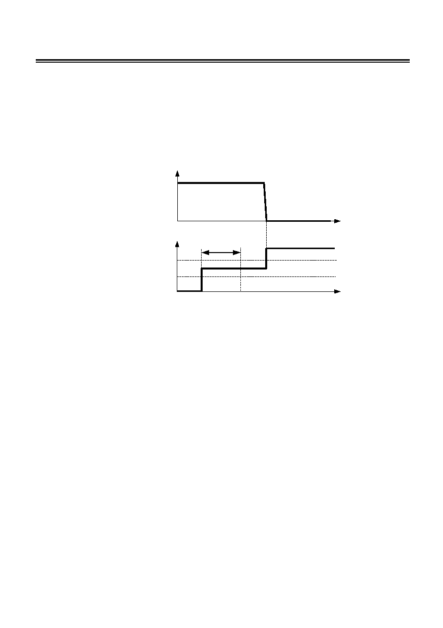
8.
Delay circuit
The detection delay times are determined by dividing a clock of approximately 3.5 kHz by the counter.
Caution The overcurrent detection delay time 2(t
IOV2
) starts when the overcurrent detection voltage
1(V
IOV1
) is detected. As soon as the overcurrent detection voltage 2(V
IOV2
) is detected over
the detection delay time for overcurrent 2(t
IOV2
) after the detection of overcurrent 1, the
S-8242 turns the discharging control FET off.
DO pin voltage
VM pin voltage
V
DD
V
SS
Overcurrent detection
delay time 2 (t
IOV2
)
V
IOV2
Time
V
DD
V
SS
Time
V
IOV1
Figure 5
Caution When overcurrent is detected and continues for longer than the overdischarge detection
delay time (t
DL
) without the load being released, the status changes to the power-down
status when the battery voltage falls below overdischarge detection voltage n (V
DLn
).
When the battery voltage falls below overdischarge detection voltage n (V
DLn
) due to
overcurrent, the S-8242 Series turns the discharging control FET off via overcurrent
detection. In this case the recovery of the battery voltage is so slow that if the battery
voltage after the overdischarge detection delay time is still lower than the overdischarge
detection voltage, the S-8242 Series shifts to the power-down status.
BATTERY PROTECTION IC FOR 2-SERIAL-CELL PACK
Rev.1.0
_00
S-8242 Series
Seiko Instruments Inc.
15
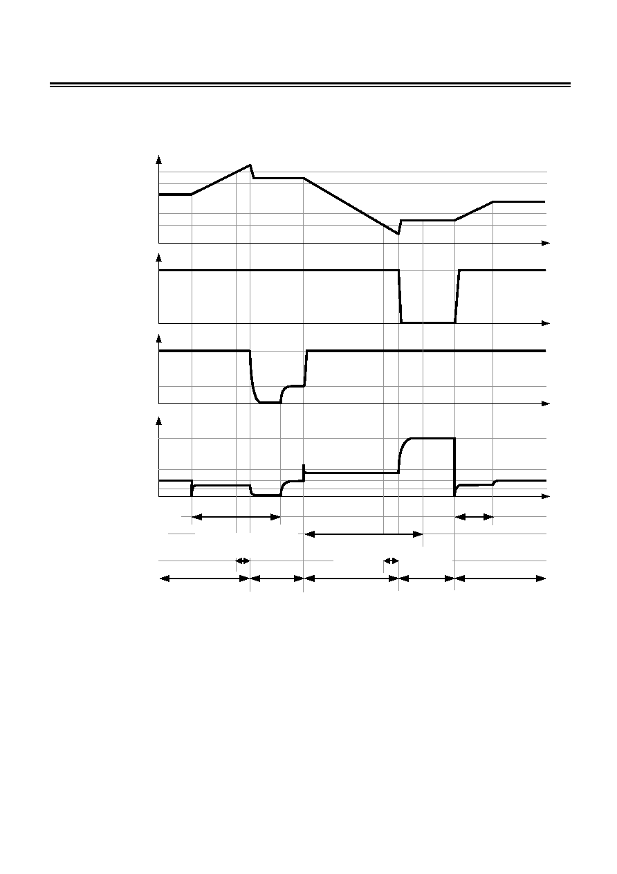
Operation Timing Chart
1. Overcharge detection, overdischarge detection
(n= 1, 2)
V
CUn
V
DUn
V
DLn
V
CLn
Battery
voltage
V
SS
CO pin
voltage
V
DD
DO pin
voltage
V
SS
Charger connection
Load connection
Mode
*1
Overcharge detection
delay time(t
CU
)
Overdischarge detection
delay time (t
DL
)
<1> <2> <1> <3> <1>
V
IOV1
V
SS
VM pin
voltage
V
DD
V
EB
-
V
DD
V
CHA
V
EB
-
*1. <1>: Normal mode
<2>: Overcharge mode
<3>: Overdischarge mode
Remark The charger is assumed to charge with a constant current.
Figure 6

BATTERY PROTECTION IC FOR 2-SERIAL-CELL PACK
S-8242 Series
Rev.1.0
_00
Seiko Instruments Inc.
16
2. Overcurrent detection
V
CUn
V
DUn
V
DLn
(n= 1, 2)
V
CLn
Battery
voltage
V
DD
DO pin
voltage
V
SS
V
DD
V
SS
CO pin
voltage
V
DD
V
SS
VM pin
voltage
V
SHORT
Charger
connection
Mode
*1
Overcurrent detection
delay time 1 (t
IOV1
)
<1> <2>
<1>
<1>
Overcurrent detection
delay time 2 (t
IOV2
)
<2>
V
IOV2
V
IOV1
*1. <1>: Normal mode
<2>: Overcurrent mode
Remark The charger is assumed to charge with a constant current.
Figure 7

BATTERY PROTECTION IC FOR 2-SERIAL-CELL PACK
Rev.1.0
_00
S-8242 Series
Seiko Instruments Inc.
17
3. Charger detection
V
CUn
V
DUn
V
DLn
(n= 1, 2)
V
CLn
Battery
voltage
V
DD
DO pin
voltage
V
SS
V
DD
V
SS
CO pin
vodltage
V
DD
V
SS
VM pin
voltage
V
CHA
Load connection
Mode
*1
Overdischarge detection delay time (t
DL
)
<1> <3>
<2>
Charger connection
VM pin vodltage
< V
CHA
Overdischarge detection (V
DL
)
*1. <1>: Normal mode
<2>: Overdischarge mode
Remark The charger is assumed to charge with a constant current.
Figure 8

BATTERY PROTECTION IC FOR 2-SERIAL-CELL PACK
S-8242 Series
Rev.1.0
_00
Seiko Instruments Inc.
18
4. Abnormal charge current detection
V
CUn
V
DUn
V
DLn
(n= 1, 2)
V
CLn
Battery
voltage
V
DD
DO pin
voltage
V
SS
V
DD
V
SS
CO pin
voltage
V
DD
V
SS
VM pin
voltage
V
CHA
Load connection
Mode
*1
Overdischarge detection delay time (t
DL
)
<1> <1>
<3>
Charger connection
V
EB
-
V
EB
-
(Overcharge detection delay time (t
CU
))
<2> <1>
*1. <1>: Normal mode
<2>: Overcharge mode
<3>: Overdischarge mode
Remark The charger is assumed to charge with a constant current.
Figure 9

BATTERY PROTECTION IC FOR 2-SERIAL-CELL PACK
Rev.1.0
_00
S-8242 Series
Seiko Instruments Inc.
19
Standard Circuit
EB+
EB
-
S-8242 Series
VSS
Battery1
DO
VDD
R3
C1
CO
VM
FET1
FET2
R1
VC
Battery2
C2
R2
Figure 10
Table 6 Constants for External Components
Symbol Part
Purpose
Recommended
Value
Min. Max.
Remarks
FET1
N-channel
MOSFET
Discharge control
Threshold voltage
Overdischarge detection
voltage
*1
Gate to source withstanding voltage
Charger
voltage
*2
FET2
N-channel
MOSFET
Charge control
Threshold voltage
Overdischarge detection
voltage
*1
Gate to source withstanding voltage
Charger
voltage
*2
R1 Resistor
ESD protection
For power
fluctuation
470
300
1
k
Resistance should be as small as possible to
avoid lowering the overcharge detection
accuracy due to current consumption.
*3
C1 Capacitor
For power
fluctuation
0.1
ĶF 0.022
ĶF 1.0
ĶF
Connect a capacitor of 0.022
ĶF or higher
between VDD and VSS.
*4
R2 Resistor
ESD protection
For power
fluctuation
470
300
1
k
Make the input filter constant of the VDD pin and the
VC pin same.
C2 Capacitor
For power
fluctuation
0.1
ĶF 0.022
ĶF 1.0
ĶF
Install a capacitor of 0.022
ĶF or higher between
VC and VSS.
*4
R3 Resistor
Protection for
reverse connection
of a charger
2 k
300
4
k
Select as large a resistance as possible to prevent
current when a charger is connected in reverse.
*5
*1. If the threshold voltage of an FET is low, the FET may not cut the charging current.
If an FET with a threshold voltage equal to or higher than the overdischarge detection voltage is used, discharging
may be stopped before overdischarge is detected.
*2. If the withstanding voltage between the gate and source is lower than the charger voltage, the FET may be destroyed.
*3. If R1 has a high resistance, the voltage between VDD and VSS may exceed the absolute maximum rating when a
charger is connected in reverse since the current flows from the charger to the IC.
Insert a resistor of 300
or higher as R1 for ESD protection.
*4. If a capacitor of less than 0.022
ĶF is connected as C1, DO may oscillate when load short-circuiting is detected. Be
sure to connect a capacitor of 0.022
ĶF or higher as C1.
*5. If R3 has a resistance higher than 4 k
, the charging current may not be cut when a high-voltage charger is
connected.
Caution The standard circuit above does not guarantee proper operation.
Evaluation in the actual application is needed to determine the correct constants.

BATTERY PROTECTION IC FOR 2-SERIAL-CELL PACK
S-8242 Series
Rev.1.0
_00
Seiko Instruments Inc.
20
Precautions
∑
The application conditions for the input voltage, output voltage, and load current should not exceed the
package power dissipation.
∑
Batteries can be connected in any order; however, there may be cases when discharging cannot be
performed when a battery is connected. In this case, short the VM and VSS pins or connect the battery
charger to return to the normal status.
∑
Do not expose this IC to an electrostatic discharge that exceeds the performance ratings of the built-in
electrostatic protection circuit.
∑
SII claims no responsibility for any disputes arising out of or in connection with any infringement by
products including this IC of patents owned by a third party.
BATTERY PROTECTION IC FOR 2-SERIAL-CELL PACK
Rev.1.0
_00
S-8242 Series
Seiko Instruments Inc.
21
Characteristics (Typical Data)
(1) Current consumption
1. I
OPE
- V
DD
2. I
OPE
- Ta
I
OPE
[
Ķ
A]
2
3
4
5
6
12
10
8
6
4
2
0
7
8
9
10
I
OPE
[
Ķ
A]
-40
-25
0
25
50
75
85
12
10
8
6
4
2
0
V
DD
[V]
Ta [
įC]
3. I
PDN
- V
DD
4. I
PDN
- Ta
I
PD
N
[
Ķ
A]
0.10
0.09
0.08
0.07
0.06
0.05
0.04
0.03
0.02
0.01
0
2
3
4
5
6
7
8
9
10
I
PD
N
[
Ķ
A]
-40
-25
0
25
50
75
85
0.10
0.09
0.08
0.07
0.06
0.05
0.04
0.03
0.02
0.01
0
V
DD
[V]
Ta [
įC]
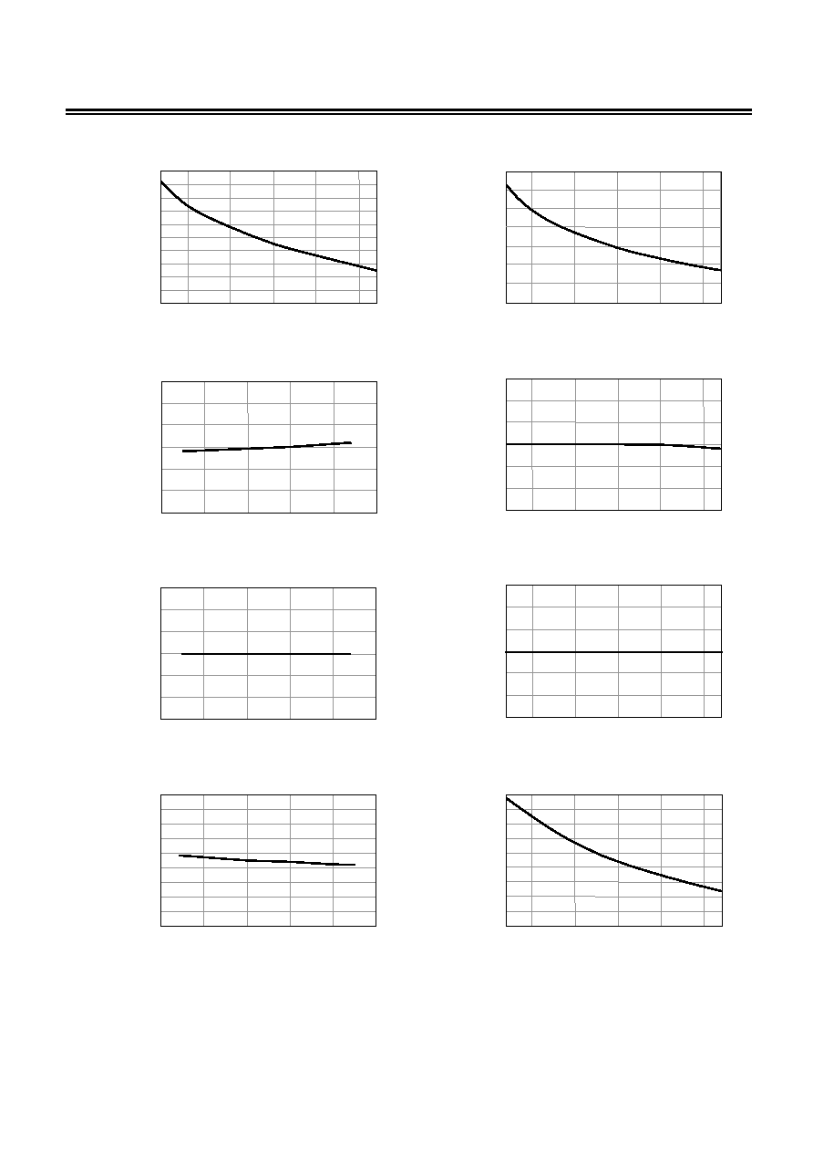
(2) Overcharge detection/release voltage, overdischarge detection/release voltage, overcurrent detection
voltage, and delay time
1. V
CU
- Ta
2. V
CL
- Ta
V
CU
[V]
4.350
4.345
4.340
4.335
4.330
4.325
4.320
4.315
4.310
4.305
4.300
-40
-25
0
25
50
75
85
V
CL
[V]
-40
-25
0
25
50
75
85
4.125
4.115
4.105
4.095
4.085
4.075
4.065
4.055
4.045
4.035
4.025
Ta [
įC]
Ta [
įC]
3. V
DU
- Ta
4. V
DL
- Ta
V
DU
[V]
-40
-25
0
25
50
75
85
3.00
2.95
2.90
2.85
2.80
V
DL
[V]
-40
-25
0
25
50
75
85
2.25
2.24
2.23
2.22
2.21
2.20
2.19
2.18
2.17
2.16
2.15
Ta [
įC]
Ta [
įC]
BATTERY PROTECTION IC FOR 2-SERIAL-CELL PACK
S-8242 Series
Rev.1.0
_00
Seiko Instruments Inc.
22
5. t
CU
- Ta
6. t
DL
- Ta
t
CU
[s]
-40
-25
0
25
50
75
85
1.42
1.37
1.32
1.27
1.22
1.17
1.12
1.07
1.02
0.97
0.92
t
DL
[m
s]
-40
-25
0
25
50
75
85
185
175
165
155
145
135
125
115
Ta [
įC]
Ta [
įC]
7. V
IOV1
- V
DD
8. V
IOV1
- Ta
V
IO
V
1
[V]
0.225
0.220
0.215
0.210
0.205
0.200
0.195
4
5
7
8
9
6
V
IO
V
1
[V]
-40
-25
0
25
50
75
85
0.225
0.220
0.215
0.210
0.205
0.200
0.195
V
DD
[V]
Ta [
įC]
9. V
IOV2
- V
DD
10. V
IOV2
- Ta
V
IO
V
2
[V]
1.5
1.4
1.3
1.2
1.1
1.0
0.9
4
5
7
8
9
6
V
IO
V
2
[V]
-40
-25
0
25
50
75
85
1.5
1.4
1.3
1.2
1.1
1.0
0.9
V
DD
[V]
Ta [
įC]
11. t
IOV1
- V
DD
12. t
IOV1
- Ta
t
IO
V
1
[m
s]
4
5
7
8
9
6
10.8
10.4
10.0
9.6
9.2
8.8
8.4
8.0
7.6
7.2
t
IO
V
1
[m
s]
-40
-25
0
25
50
75
85
10.8
10.4
10.0
9.6
9.2
8.8
8.4
8.0
7.6
7.2
V
DD
[V]
Ta [
įC]

BATTERY PROTECTION IC FOR 2-SERIAL-CELL PACK
Rev.1.0
_00
S-8242 Series
Seiko Instruments Inc.
23
13. t
IOV2
- V
DD
14. t
IOV2
- Ta
t
IO
V
2
[m
s]
0.38
0.36
0.34
0.32
0.30
0.28
0.26
0.24
0.22
4
5
7
8
9
6
t
IO
V
2
[m
s]
-40 -25
0
25
50
75
85
0.38
0.36
0.34
0.32
0.30
0.28
0.26
0.24
0.22
V
DD
[V]
Ta [
įC]
(3) CO/DO pin
1. I
COH
- V
CO
2. I
COL
- V
CO
I
CO
H
[m
A]
0
1
3
4
5
2
6
0
-0.2
-0.4
-0.6
-0.8
-1.0
-1.2
-1.4
-1.6
7
I
CO
L
[m
A]
1.6
1.4
1.2
1.0
0.8
0.6
0.4
0.2
0
0
1
3
4
5
2
6
7
8
9
V
CO
[V]
V
CO
[V]
3. I
DOH
- V
DO
4. I
DOL
- V
DO
I
DO
H
[m
A]
0
1
3
4
5
2
6
0
-0.2
-0.4
-0.6
-0.8
-1.0
-1.2
-1.4
7
I
DO
L
[m
A]
0.30
0.25
0.20
0.15
0.10
0.05
0
0
1
3
2
V
DO
[V]
V
DO
[V]
2.9Ī0.2
0.15
1.9Ī0.2
1
2
3
4
6
5
0.4
0.95
+0.1
-0.08
0.95
+0.1
-0.05
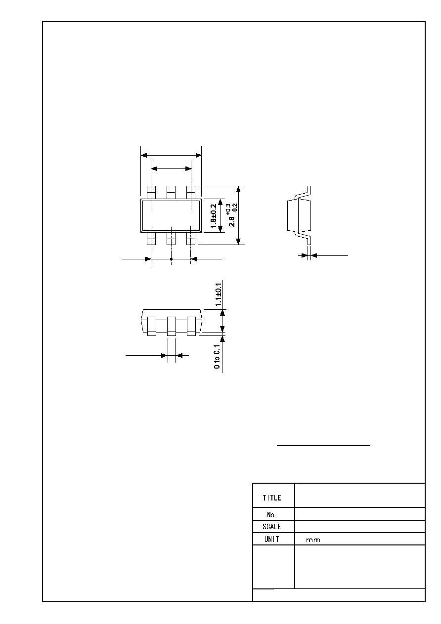
No. MP006-B-P-SD-1.0
SOT236-B-PKG Dimensions
MP006-B-P-SD-1.0
Seiko Instruments Inc.
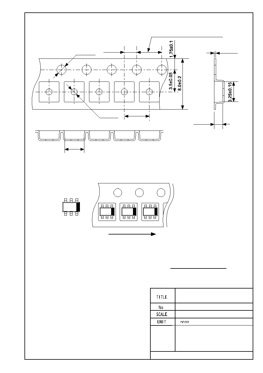
No. MP006-B-C-SD-1.0
SOT236-B-Carrier Tape
MP006-B-C-SD-1.0
Seiko Instruments Inc.
1
2
3
4 5 6
Ý1.5
+0.1
-0
2.0Ī0.05
Ý1.0
+0.2
-0
4.0Ī0.1
1.4Ī0.2
0.25Ī0.1
3.2Ī0.2
Feed direction
4.0Ī0.1(10 pitches:40.0Ī0.2)

12.5max.
9.0Ī0.3
Ý13Ī0.2
(60į)
(60į)
SOT236-B-Reel
MP006-B-R-SD-1.0
Seiko Instruments Inc.
No. MP006-B-R-SD-1.0
Enlarged drawing in the central part
1.8Ī0.15
0.5Ī0.1
0.5Ī0.1
0.8Ī0.05
0.14Ī0.05
R(0.075)
0.2Ī0.08
(0.125)
1
2
3
4
5
6
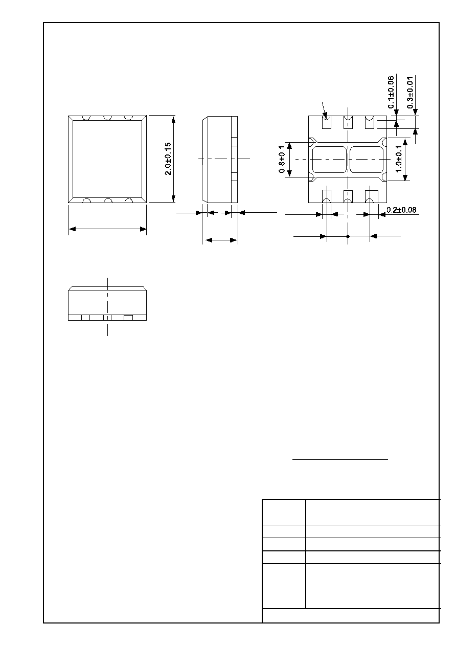
SNB6B-A-PKG Dimensions
No. BD006-A-P-SD-1.1
Seiko Instruments Inc.
No.
TITLE
SCALE
UNIT
mm
BD006-A-P-SD-1.1

No.
TITLE
SCALE
UNIT
mm
4.0Ī0.1
2.0Ī0.05
4.0Ī0.1
Ý1.5Ī0.1
2.2Ī0.1
1.1Ī0.1
0.25Ī0.05
Ý1.1Ī0.1
Seiko Instruments Inc.
Feed direction
SNB6B-A-Carrier Tape
No. BD006-A-C-SD-2.1
BD006-A-C-SD-2.1
1
2
3
6
5
4
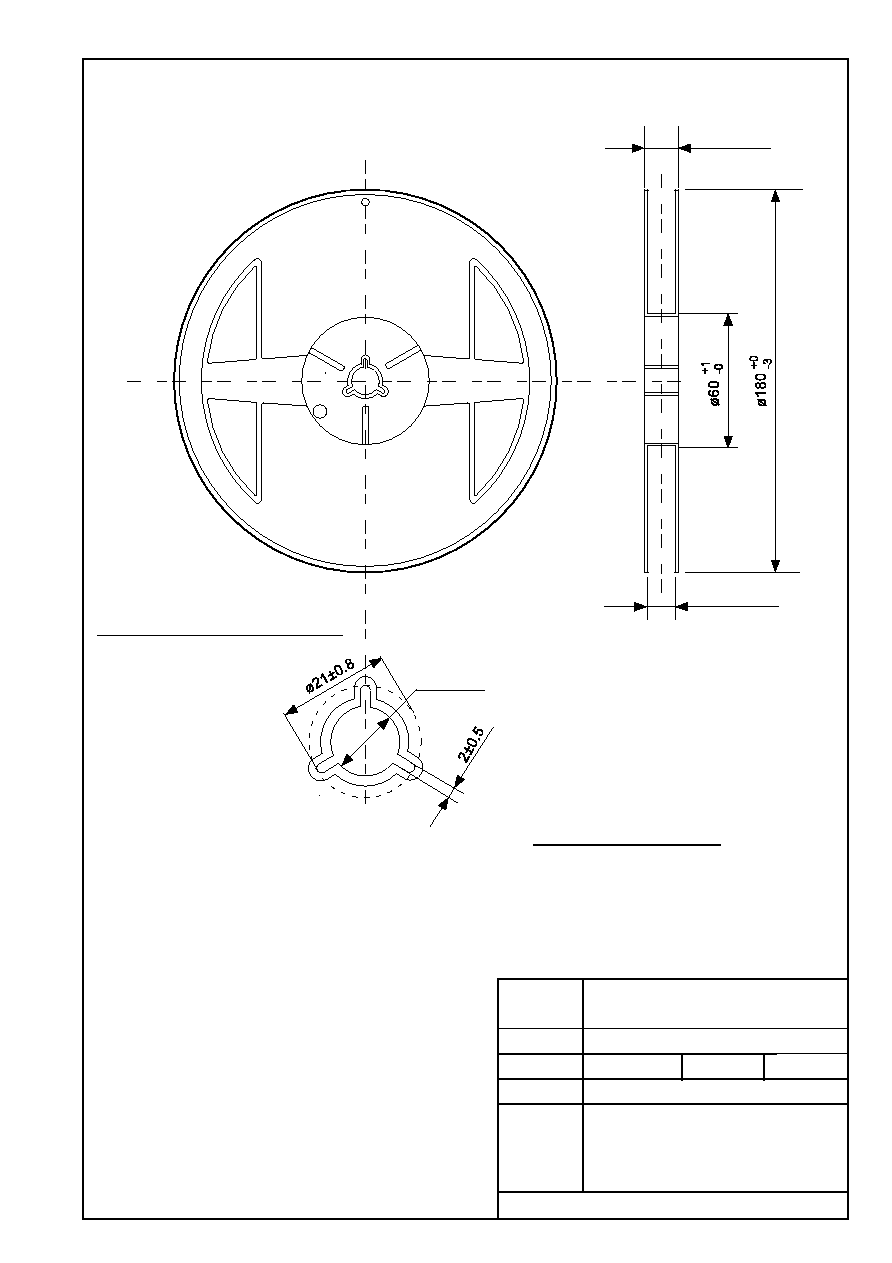
QTY.
3,000
No.
TITLE
SCALE
UNIT
mm
12.5max.
9.0Ī0.3
Ý13Ī0.2
Seiko Instruments Inc.
Enlarged drawing in the central part
SNB6B-A-Reel
No. BD006-A-R-SD-1.1
BD006-A-R-SD-1.1

∑
The information described herein is subject to change without notice.
∑
Seiko Instruments Inc. is not responsible for any problems caused by circuits or diagrams described herein
whose related industrial properties, patents, or other rights belong to third parties. The application circuit
examples explain typical applications of the products, and do not guarantee the success of any specific
mass-production design.
∑
When the products described herein are regulated products subject to the Wassenaar Arrangement or other
agreements, they may not be exported without authorization from the appropriate governmental authority.
∑
Use of the information described herein for other purposes and/or reproduction or copying without the
express permission of Seiko Instruments Inc. is strictly prohibited.
∑
The products described herein cannot be used as part of any device or equipment affecting the human
body, such as exercise equipment, medical equipment, security systems, gas equipment, or any apparatus
installed in airplanes and other vehicles, without prior written permission of Seiko Instruments Inc.
∑
Although Seiko Instruments Inc. exerts the greatest possible effort to ensure high quality and reliability, the
failure or malfunction of semiconductor products may occur. The user of these products should therefore
give thorough consideration to safety design, including redundancy, fire-prevention measures, and
malfunction prevention, to prevent any accidents, fires, or community damage that may ensue.