Document Outline
- S-8243A/B Series
- Cover
- Features
- Package
- Applications
- Block Diagrams
- Selection Guide
- Absolute Maximum Ratings
- Pin Configuration
- Electrical Characteristics
- Test Circuits
- Operation Descriptions
- Operation Timing Charts
- Standard Circuits
- Precautions
- Application Circuits
- Typical Characteristics (Typical data)
- Package Drawing

Rev.1.1
_00
BATTRY PROTECTION IC FOR 3-SERIAL OR
4-SERIAL PACK
S-8243A/B Series
Seiko Instruments Inc.
1
The S-8243A/B is a series of lithium-ion rechargeable
battery protection ICs incorporating high-accuracy
battery protection circuits, a battery monitor amp and a
voltage regulator.
The S-8243A/B is suitable for protection of 3-serial or
4- serial cell lithium-ion battery packs from
overcharge, overdischarge and overcurrent.
Features
(1) High-accuracy voltage detection for each cell
∑ Overcharge detection voltage n (n=1 to 4)
3.9 V to 4.4 V (50 mV step)
Accuracy Ī25 mV
∑ Hysteresis voltage n (n=1 to 4) of overcharge detection
-0.10 V to -0.40 V (50 mV step) or 0 V
Accuracy Ī50 mV
(Overcharge release voltage n (
=Overcharge detection voltage n + Hysteresis voltage n) can be
selected within the range 3.8 V to 4.4 V.)
∑ Overdischarge detection voltage n (n=1 to 4)
2.0 V to 3.0 V (100 mV step)
Accuracy Ī80 mV
∑ Hysteresis voltage n (n=1 to 4) of overdischarge detection
0.20 V to 0.70 V or 0 V (100 mV step)
Accuracy Ī100 mV
(Overdischarge release voltage n (
=Overdischarge detection voltage n + Hysteresis voltage n) can be
selected within the range 2.0 V to 3.4 V.)
(2) Three-level overcurrent protection including protection for short-circuiting
∑ Overcurrent detection voltage 1
0.05 V to 0.3 V (50 mV step) Accuracy Ī25 mV
∑ Overcurrent detection voltage 2
0.5 V
Accuracy Ī100 mV
∑ Overcurrent detection voltage 3
V
DD
/2
Accuracy Ī15 %
(3) Delay times for overcharge detection, overdischarge detection and overcurrent detection 1 can be set by
external capacitors.
(Delay times for overcurrent detection 2 and 3 are fixed internally.)
(4) Charge/discharge operation can be controlled through the control pins.
(5) High-accuracy battery monitor amp
GAMP
= V
BATTERY
◊ 0.2 Ī1.0%
(6) Voltage regulator
V
OUT
= 3.3 V Ī2.4 % (3 mA max.)
(7) High input-voltage device
Absolute maximum rating: 26 V
(8) Wide operating voltage range
6 V to 18 V
(9) Wide operating temperature range:
-40įC to +85 įC
(10) Low current consumption
Operation mode
120
ĶA max.
Power down mode
0.1
ĶA max.
(11) Small package
16-Pin TSSOP package
Package
∑ 16-Pin TSSOP (Package drawing code : FT016-A)
Applications
∑ Lithium-ion rechargeable battery packs
∑ Lithium- polymer rechargeable battery packs

BATTERY PROTECTION IC FOR 3-SERIAL OR 4-SERIAL PACK
S-8243A/B Series
Rev.1.1
_00
2
Seiko Instruments Inc.
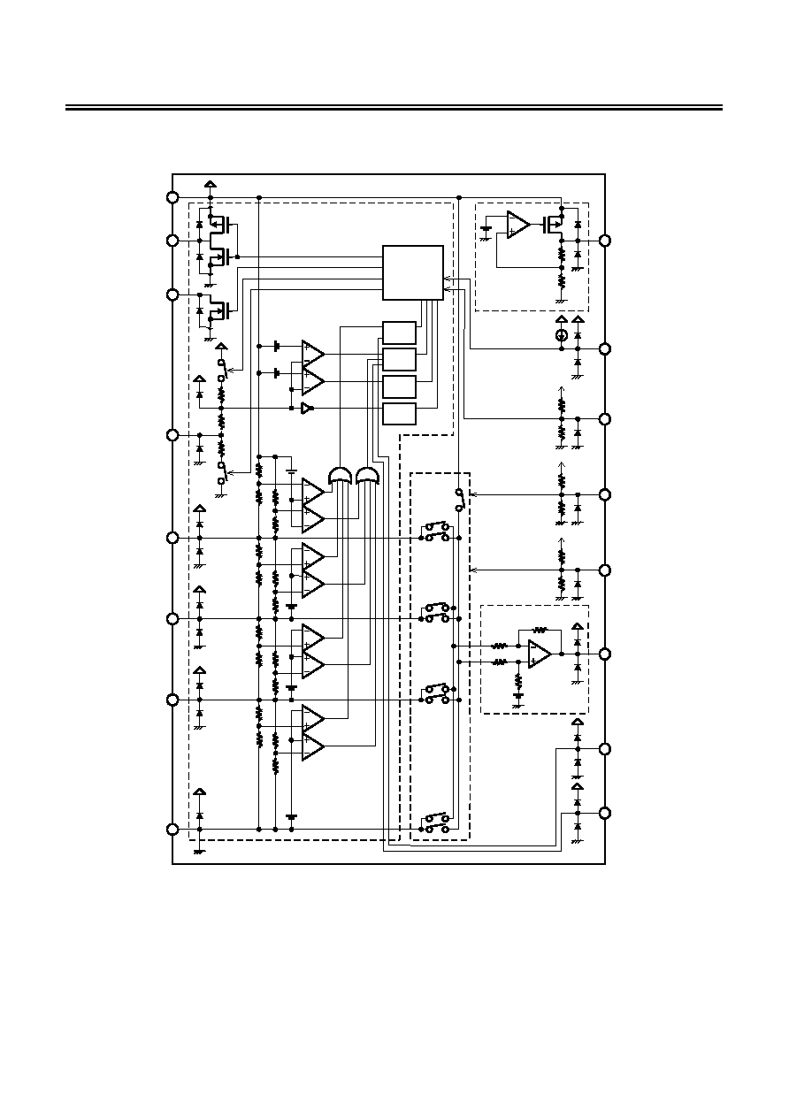
Block Diagrams
S-8243A Series
Battery protection
VC3
VC2
VC1
VDD
DOP
COP
VMP
VREG
VBATOUT
200 nA
CTL1
CTL2
CTL3
1.4 M
1.4 M
1 M
1 M
5 M
5 M
CTL4
VREG
VREG
VREG
Delay
control
RVCM,RVSM
DOP,COP,
Delay
Delay
Delay
Battery monitor amp
Voltage
regulator
1.4 M
1.4 M
1.4 M
1.4 M
660 k
660 k
440 k
CCT
VSS
CDT
Battery
selection
Remark1. Diodes in the figure are parasitic diodes.
2. Numerical values are typical values.
Figure 1
BATTERY PROTECTION IC FOR 3-SERIAL OR 4-SERIAL PACK
Rev.1.1
_00
S-8243A/B Series
Seiko Instruments Inc.
3
S-8243B Series
Battery protection
VC3
VC2
VC1
VDD
DOP
COP
VMP
VREG
VBATOUT
200 nA
CTL1
CTL2
CTL3
1.4 M
1.4 M
1 M
1 M
5 M
5 M
CTL4
VREG
VREG
VREG
Delay
control
RVCM, RVSM
DOP, COP,
Delay
Delay
Delay
Battery monitor amp
Voltage
regulator
1.4 M
1.4 M
1.4 M
1.4 M
660
k
660 k
440 k
CCT
VSS
CDT
Battery
selection
Remark1. Diodes in the figure are parasitic diodes.
2. Numerical values are typical values.
Figure 2
BATTERY PROTECTION IC FOR 3-SERIAL OR 4-SERIAL PACK
S-8243A/B Series
Rev.1.1
_00
4
Seiko Instruments Inc.
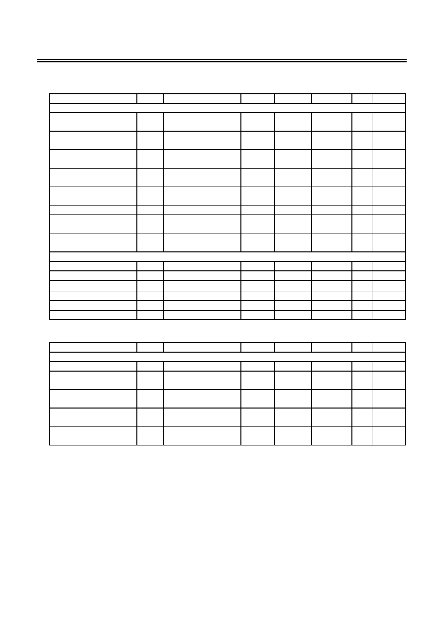
Selection Guide
S-8243A series is designed for 3-serial pack.
S-8243B series is designed for 4-serial pack.
1. S-8243A Series
Table 1
Product name
Overcharge
detection
voltage [V
CU
]
Hysteresis voltage for
overcharge detection
[V
HC
]
Overdischarge
detection voltage
[V
DL
]
Hysteresis voltage for
overdischarge
detection [V
HD
]
Overcurrent
detection
voltage1 [V
IOV1
]
0 V battery
charging
function
S-8243AACFT 4.35
Ī 0.025 V
-0.15 Ī0.05 V
2.40
Ī0.08 V
0.20
Ī0.10 V
0.20
Ī0.025 V
Available
S-8243AADFT 4.35
Ī 0.025 V
-0.35 Ī0.05 V
2.40
Ī0.08 V
0 V
0.20
Ī0.025 V
Available
Note Change in the detection voltage is available in products other than listed above. Contact the SII sales office.
2. S-8243B Series
Table 2
Product name
Overcharge
detection
voltage [V
CU
]
Hysteresis voltage for
overcharge detection
[V
HC
]
Overdischarge
detection voltage
[V
DL
]
Hysteresis voltage for
overdischarge
detection
Overcurrent
detection
voltage1
0 V battery
charging
function
S-8243BADFT 4.35
Ī0.025 V
-0.25 Ī0.05 V
2.40
Ī0.08 V
0 V
0.25
Ī0.025 V
Available
S-8243BAEFT 4.35
Ī0.025 V
-0.15 Ī0.05 V
2.40
Ī0.08 V
0.20
Ī0.10 V
0.20
Ī0.025 V
Available
S-8243BAFFT 4.25
Ī0.025 V
-0.25 Ī0.05 V
2.40
Ī0.08 V
0 V
0.20
Ī0.025 V
Available
Note Change in the detection voltage is available in products other than listed above. Contact the SII sales office.
Absolute Maximum Ratings
Table 3
(Ta
= 25įC unless otherwise specified)
Parameter Symbol
Applied
Pins
Rating
Unit
Input voltage VDD
V
DS
V
SS
-0.3 to V
SS
+26
V
Input voltage
V
IN
VC1, VC2, VC3, CCT, CDT
V
SS
-0.3 to V
DD
+0.3
V
VMP pin Input voltage
V
MP
VMP
V
SS
-0.3 to V
SS
+26
V
DOP pin output voltage
V
DOP
DOP
V
SS
-0.3 to V
DD
+0.3
V
COP pin output voltage
V
COP
COP
V
SS
-0.3 to V
SS
+26
V
VREG pin output voltage
V
OUT
VREG
V
SS
-0.3 to V
DD
+0.3
V
CTL1 pin input voltage
V
CTL1
CTL1
V
SS
-0.3 to V
DD
+0.3
V
CTL2 to CTL4 pin input voltage
V
CTLn
CTL2, CTL3, CTL4
V
SS
-0.3 to V
OUT
+0.3
V
Cell voltage output voltage
V
BATOUT
VBATOUT V
SS
-0.3 to V
OUT
+0.3
V
Power dissipation
P
D
300 mW
Operating temperature range
T
opr
-40 to +85
įC
Storage temperature range
T
stg
-40 to +125
įC
Caution The absolute maximum ratings are rated values exceeding which the product could suffer physical
damage. These values must therefore not be exceeded under any conditions.
BATTERY PROTECTION IC FOR 3-SERIAL OR 4-SERIAL PACK
Rev.1.1
_00
S-8243A/B Series
Seiko Instruments Inc.
5
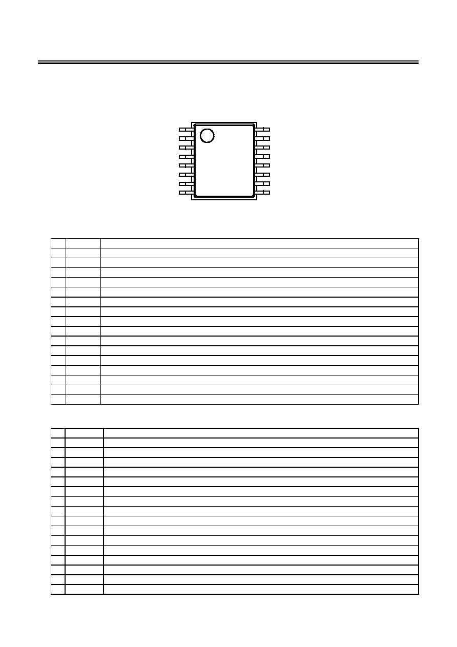
Pin Configuration
16-Pin TSSOP
Top view
VDD
DOP
COP
VMP
VC1
VC2
VC3
VSS
VREG
CTL1
CTL2
CTL3
CTL4
VBATOUT
CCT
CDT
1
2
3
4
5
6
7
8
16
15
14
13
12
11
10
9
Figure 3
Table 4 Pin description (S-8243A Series)
No. Name
Description
1
VDD
Positive power input pin. Battery 1 positive voltage connection pin
2
DOP
FET gate connection pin for discharge control (CMOS output)
3
COP
FET gate connection pin for charge control (Nch open-drain output)
4
VMP
Voltage detection pin between VDD and VMP (Over current detection pin)
5 VC1
No
connection
6
VC2
Battery1 negative voltage and battery 2 positive voltage connection pin
7
VC3
Battery 2 negative voltage and battery 3 positive voltage connection pin
8
VSS
Negative power input pin. Battery 3 negative voltage connection pin
9
CDT
Capacitor connection pin for overdischarge detection delay time and over current detection1 delay time
10
CCT
Capacitor connection pin for overcharge detection delay time
11 VBATOUT Output pin for each battery voltage and offset
12
CTL4
Battery selection control signal input
13
CTL3
Battery selection control signal input
14
CTL2
Charge and discharge control signal input
15
CTL1
Charge and discharge control signal input
16
VREG 3.3 V voltage regulator output
Table 5 Pin description (S-8243B Series)
No. Name
Description
1
VDD
Positive power input pin. Battery 1 positive voltage connection pin
2
DOP
FET gate connection pin for discharge control (CMOS output)
3
COP
FET gate connection pin for charge control (Nch open-drain output)
4
VMP
Voltage detection pin between VDD and VMP (Over current detection pin)
5
VC1
Battery1 negative voltage and battery 2 positive voltage connection pin
6
VC2
Battery 2 negative voltage and battery 3 positive voltage connection pin
7
VC3
Battery 3 negative voltage and battery 4 positive voltage connection pin
8
VSS
Negative power input pin. Battery 4 negative voltage connection pin
9
CDT
Capacitor connection pin for overdischarge detection delay time and over current detection1 delay time
10
CCT
Capacitor connection pin for overcharge detection delay time
11 VBATOUT Output pin for each battery voltage and offset
12
CTL4
Battery selection control signal input
13
CTL3
Battery selection control signal input
14
CTL2
Charge and discharge control signal input
15
CTL1
Charge and discharge control signal input
16
VREG
3.3 V voltage regulator output
BATTERY PROTECTION IC FOR 3-SERIAL OR 4-SERIAL PACK
S-8243A/B Series
Rev.1.1
_00
6
Seiko Instruments Inc.
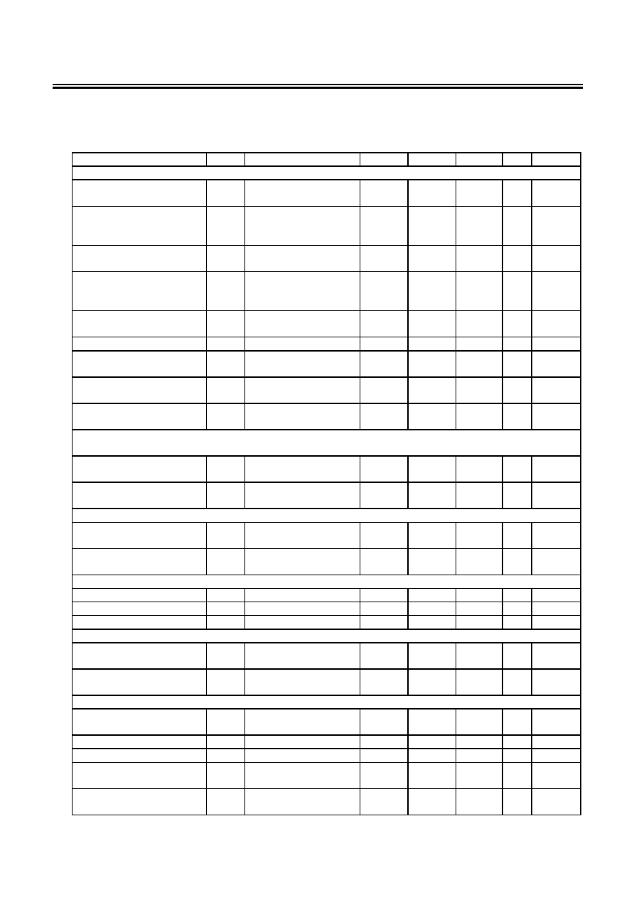
Electrical Characteristics
(1) S-8243A Series
Table 6 (1/2)
(Ta
= 25 įC unless otherwise specified)
Parameter Symbol
Conditions Min.
Typ.
Max.
Unit
Test
circuit
BATTERY PROTECTION
Overcharge detection voltage n
n
=1, 2, 3
V
CUn
3.9 V to 4.4 V, 50 mV Step
V
CUn
-
0.025
V
CUn
V
CUn
+0.025
V 4
Hysteresis voltage n of
overcharge detection
n
=1, 2, 3
V
HCn
-0.10 V to -0.40 V, and 0 V
V
HCn
-0.05
V
HCn
V
HCn
+0.05
V 4
Overdischarge detection voltage
n
=1, 2, 3
V
DLn
2.0 V to 3.0 V, 100 mV Step
V
DLn
-
0.08
V
DLn
V
DLn
+0.08
V 4
Hysteresis voltage n of
Overdischarge detection
n
=1, 2, 3
V
HDn
0.20 V to 0.70 V, and 0 V
V
HDn
-0.10
V
HDn
V
HDn
+0.10
V 4
Overcurrent detection voltage 1 V
IOV1
0.05 V to 0.3 V, 50 mV Step
V
IOV1
-
0.025
V
IOV1
V
IOV1
+0.025
V 4
Overcurrent detection voltage 2 V
IOV2
V
DD
-
0.60 V
DD
-
0.50 V
DD
-
0.40
V 4
Overcurrent detection voltage 3 V
IOV3
V
DD
◊0.425 V
DD
◊0.5 V
DD
◊0.575 V
4
Temperature coefficient for
detection and release voltage
*1
T
COE1
Ta
=
-
5
įC to +55 įC
-
1.0
0 1.0
mV/
įC 4
Temperature coefficient for
overcurrent detection voltage
*2
T
COE2
Ta
=
-
5
įC to +55 įC
-
0.5
0 0.5
mV/
įC 4
0 V BATTERY CHARGING FUNCTION
0 V battery charge starting
charger voltage
V
0CHA
0 V battery charging available
0.8 1.5
V
7
0 V battery charge inhibition
battery voltage
V
0INH
0 V battery charging unavailable
0.4 0.7 1.1 V 7
INTERNAL RESISTANCE
Internal resistance between
VMP and VDD
R
VDM
V1
=V2=V3=3.5 V
500
1100
2400
k
8
Internal resistance between
VMP and VSS
R
VSM
V1
=V2=V3=1.8 V
300
700
1500
k
8
VOLTAGE REGULATOR
Output voltage
V
OUT
V
DD
=14 V, I
OUT
=3 mA
3.221
3.300
3.379
V
2
Line regulation
V
OUT1
V
DD
=6 V18 V, I
OUT
=3 mA
5 15
mV
2
Load regulation
V
OUT2
V
DD
=14 V, I
OUT
=5 ĶA3 mA
15 30
mV
2
BATTERY MONITOR AMP
Input offset voltage n
n
=1, 2, 3
V
OFFn
V1
=V2=V3=3.5 V
60
165
270
mV
3
Voltage gain n
n
=1, 2, 3
GAMPn V1
=V2=V3=3.5 V
0.2
◊0.99 0.2 0.2◊1.01
3
INPUT VOLTAGE, OPERATING VOLTAGE
Operating voltage between V
DD
and V
SS
V
DSOP
6
18 V 4
CTL1 input voltage for High
V
CTL1H
V
DD
◊0.8
V 6
CTL1 input voltage for Low
V
CTL1L
V
DD
◊0.2 V 6
CTLn input voltage for High
n
=2, 3, 4
V
CTLnH
V
OUT
◊0.9
V
OUT
V 3,
6
CTLn input voltage for Low
n
=2, 3, 4
V
CTLnL
V
OUT
◊0.1 V 3,
6
BATTERY PROTECTION IC FOR 3-SERIAL OR 4-SERIAL PACK
Rev.1.1
_00
S-8243A/B Series
Seiko Instruments Inc.
7
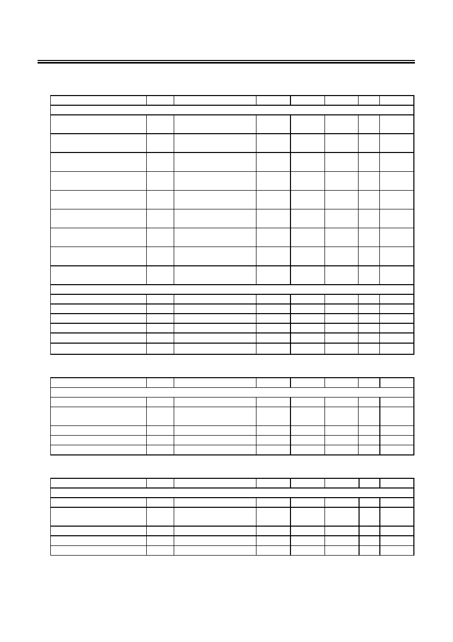
Table 6 (2/2)
Parameter Symbol Remarks Min.
Typ.
Max.
Unit
Test
circuit
INPUT CURRENT
Current consumption at not
monitoring V
BATOUT
I
OPE
V1
=V2=V3=3.5 V, V
MP
=V
DD
65 120
ĶA 1
Current consumption at power
down
I
PDN
V1
=V2=V3=1.5 V, V
MP
=V
SS
0.1
ĶA 1
Current for VCN at not
monitoring V
BATOUT
(n
=2, 3)
I
VCnN
V1
=V2=V3=3.5 V
-0.3 0 0.3
ĶA 3
Current for VC2 at monitoring of
V
BATOUT
I
VC2
V1
=V2=V3=3.5 V
2.0 7.2
ĶA 3
Current for VC3 at monitoring of
V
BATOUT
I
VC3
V1
=V2=V3=3.5 V
1.0 4.0
ĶA 3
Current for CTL1 at Low
I
CTL1L
V1
=V2=V3=3.5 V, V
CTL1
=0 V
-0.4
-0.2
ĶA 5
Current for CTLn at High
n
=2,3,4
I
CTLnH
V
CTLn
=V
OUT
2.5 5
ĶA 9
Current for CTLn at Low
n
=2,3,4
I
CTLnL
V
CTLn
=0 V
-5
-2.5
ĶA 9
OUTPUT CURRENT
Leak current COP
I
COH
V
COP
=24 V
0.1
ĶA 9
Sink current COP
I
COL
V
COP
=V
SS
+0.5 V
10
ĶA 9
Source current DOP
I
DOH
V
DOP
=V
DD
-
0.5 V
10
ĶA 9
Sink current DOP
I
DOL
V
DOP
=V
SS
+0.5 V
10
ĶA 9
Source current V
BATOUT
I
VBATH
V
BATOUT
=V
DD
-
0.5 V
100
ĶA 9
Sink current V
BATOUT
I
VBATL
V
BATOUT
=V
SS
+0.5 V
100
ĶA 9
Applied to S-8243AACFT and S-8243AADFT
Parameter Symbol
Conditions Min.
Typ.
Max.
Unit
Test
circuit
DELAY TIME
Overcharge detection delay time
t
CU
C
CT
=0.1 ĶF 0.5
1.0
1.5
s
5
Overdischarge detection delay
time
t
DL
C
DT
=0.1 ĶF
50 100
150 ms 5
Overcurrent detection delay
time 1
t
lOV1
C
DT
=0.1 ĶF 5
10
15
ms
5
Overcurrent detection delay
time 2
t
lOV2
1.5
2.5
4.0
ms
4
Overcurrent detection delay
time 3
t
lOV3
100
300
600
Ķs 4
*1. Temperature coefficient for detection and release voltage is applied to overcharge detection voltage n, overcharge release voltage n
overdischarge detection voltage n, and overdischarge release voltage n.
*2. Temperature coefficient for overcurrent detection voltage is applied to over current detection voltage 1 and 2.
BATTERY PROTECTION IC FOR 3-SERIAL OR 4-SERIAL PACK
S-8243A/B Series
Rev.1.1
_00
8
Seiko Instruments Inc.
(2) S-8243B Series
Table 7 (1/2)
(Ta
= 25įC unless otherwise specified)
Parameter Symbol
Conditions Min.
Typ.
Max.
Unit
Test
circuit
DETECTION VOLTAGE
Overcharge detection voltage n
n
=1, 2, 3, 4
V
CUn
3.9 V to 4.4 V, 50 mV Step
V
CUn
-0.025
V
Cun
V
CUn
+0.025
V 4
Hysteresis voltage n of overcharge
detection
n
=1, 2, 3, 4
V
HCn
-0.10 V to -0.40 V, and 0 V
V
HCn
-0.05
V
HCn
V
HCn
+0.05
V 4
Overdischarge detection voltage
n
=1, 2, 3, 4
V
DLn
2.0 V to 3.0 V, 100 mV Step
V
DLn
-0.08
V
DLn
V
DLn
+0.08
V 4
Hysteresis voltage n of
overdischarge detection
n
=1, 2, 3, 4
V
HDn
0.20 to 0.70, and 0
V
HDn
-0.10
V
HDn
V
HDn
+0.10
V 4
Overcurrent detection voltage 1
V
IOV1
0.05 V to 0.3 V, 50 mV Step
V
IOV1
-0.025
V
IOV1
V
IOV1
+0.025
V 4
Overcurrent detection voltage 2
V
IOV2
V
DD
-0.60 V
DD
-0.50 V
DD
-0.40 V
4
Overcurrent detection voltage 3
V
IOV3
V
DD
◊0.425
V
DD
◊0.5
V
DD
◊0.575
V 4
Temperature coefficient for
detection and release voltage
*1
T
COE1
Ta
= -5įC to +55įC
-1.0 0 1.0
mV/
įC 4
Temperature coefficient for
overcurrent detection voltage
*2
T
COE2
Ta
= -5įC to +55įC
-0.5 0 0.5
mV/
įC 4
0 V BATTERY CHARGING FUNCTION (The 0 V battery function is either "0 V battery charging is allowed." or "0 V battery charging is
inhibited." depending upon the product type.)
0 V battery charge starting charger
voltage
V
0CHA
0 V battery charging allowed
0.8 1.5
V 7
0 V battery charge inhibition
battery voltage
V
0INH
0 V battery charging inhibited
0.4
0.7
1.1
V
7
INTERNAL RESISTANCE
Internal resistance between VMP
and VDD
R
VDM
V1
=V2=V3=V4=3.5 V
500
1100
2400
k
8
Internal resistance between VMP
and VSS
R
VSM
V1
=V2=V3=V4=1.8 V
300
700
1500
k
8
VOLTAGE REGULATOR
Output voltage
V
OUT
V
DD
=14V, I
OUT
=3 mA
3.221
3.300
3.379
V
2
Line regulation
V
OUT1
V
DD
=6 V18 V, I
OUT
=3 mA
5 15
mV
2
Load regulation
V
OUT2
V
DD
=14 V, I
OUT
=5 ĶA3 mA
15 30
mV
2
BATTERY MONITOR AMP
Input offset voltage n
n
=1, 2, 3, 4
V
OFFn
V1
=V2=V3= V4=3.5 V
60
165
270
mV
3
Voltage gain n
n
=1, 2, 3, 4
GAMPn V1
=V2=V3= V4=3.5 V
0.2
◊0.99 0.2 0.2◊1.01
3
INPUT VOLTAGE, OPERATING VOLTAGE
Operating voltage between V
DD
and V
SS
V
DSOP
6
18
V 4
CTL1 input voltage for High
V
CTL1H
V
DD
◊0.8
V 6
CTL1 input voltage for Low
V
CTL1L
V
DD
◊0.2 V
6
CTLn input voltage for High
n
=2, 3, 4
V
CTLnH
V
OUT
◊0.9
V
OUT
V 3,
6
CTLn input voltage for Low
n
=2, 3, 4
V
CTLnL
V
OUT
◊0.1 V
3,
6
BATTERY PROTECTION IC FOR 3-SERIAL OR 4-SERIAL PACK
Rev.1.1
_00
S-8243A/B Series
Seiko Instruments Inc.
9
Table 7 (2/2)
Parameter Symbol
Remarks Min.
Typ.
Max.
Unit
Test
circuit
INPUT CURRENT
Current consumption at not
monitoring V
BATOUT
I
OPE
V1
=V2=V3=V4=3.5 V,
V
MP
=V
DD
65 120
ĶA 1
Current consumption at power
down
I
PDN
V1
=V2=V3=V4=1.5 V,
V
MP
=V
SS
0.1
ĶA 1
Current for VCn at not monitoring
V
BATOUT
(n
=1, 2, 3)
I
VCnN
V1
=V2=V3=V4=3.5 V
-0.3 0 0.3
ĶA 3
Current for VC1 at monitoring of
V
BATOUT
I
VC1
V1
=V2=V3=V4=3.5 V
3.2 10.4
ĶA 3
Current for VC2 at monitoring of
V
BATOUT
I
VC2
V1
=V2=V3=V4=3.5 V
2.0 7.2
ĶA 3
Current for VC3 at monitoring of
V
BATOUT
I
VC3
V1
=V2=V3=V4=3.5 V,
V
CTL1
=0 V
1.0 4.0
ĶA 3
Current for CTL1 at Low
I
CTL1L
V1
=V2=V3=V4=3.5 V,
V
CTL1
=0 V
-0.4
-0.2
ĶA 5
Current for CTLn at High
n
=2, 3, 4
I
CTLnH
V
CTLn
=V
OUT
2.5 5
ĶA 9
Current for CTLn at Low
n
=2, 3, 4
I
CTLnL
V
CTLn
=0 V
-5
-2.5
ĶA 9
OUTPUT CURRENT
Leak current COP
I
COH
V
COP
=24 V
0.1
ĶA 9
Sink current COP
I
COL
V
COP
=V
SS
+0.5 V
10
ĶA 9
Source current DOP
I
DOH
V
DOP
=V
DD
-0.5 V
10
ĶA 9
Sink current DOP
I
DOL
V
DOP
=V
SS
+0.5 V
10
ĶA 9
Source current V
BATOUT
I
VBATH
V
BATOUT
=V
DD
-0.5 V
100
ĶA 9
Sink current V
BATOUT
I
VBATL
V
BATOUT
=V
SS
+0.5 V
100
ĶA 9
Applied to S-8243BAEFT and S-8243BAFFT
Parameter Symbol
Conditions Min.
Typ.
Max.
Unit
Test
circuit
DELAY TIME
Overcharge detection delay time
t
CU
C
CT
=0.1 ĶF 0.5
1.0
1.5
s
5
Overdischarge detection delay
time
t
DL
C
DT
=0.1 ĶF 50
100
150
ms
5
Overcurrent detection delay time 1
t
lOV1
C
DT
=0.1 ĶF 5
10
15
ms
5
Overcurrent detection delay time 2
t
lOV2
1.5
2.5
4.0
ms
4
Overcurrent detection delay time 3
t
lOV3
100
300
600
Ķs 4
Applied to S-8243BADFT
Parameter Symbol
Conditions Min.
Typ.
Max.
Unit
Test
circuit
DELAY TIME
Overcharge detection delay time
t
CU
C
CT
=0.1 ĶF
0.5 1.0 1.5
s 5
Overdischarge detection delay
time
t
DL
C
DT
=0.1 ĶF 55.5
111
222
ms
5
Overcurrent detection delay time 1
t
lOV1
C
DT
=0.1 ĶF
3.31 6.62 13.2
ms 5
Overcurrent detection delay time 2
t
lOV2
1.5 2.5 4.0
ms
4
Overcurrent detection delay time 3
t
lOV3
100 300 600
Ķs 4
*1. Temperature coefficient for detection and release voltage is applied to overcharge detection voltage n, overcharge release voltage n
overdischarge detection voltage n, and overdischarge release voltage n.
*2. Temperature coefficient for overcurrent detection voltage is applied to over current detection voltage 1 and 2.

BATTERY PROTECTION IC FOR 3-SERIAL OR 4-SERIAL PACK
S-8243A/B Series
Rev.1.1
_00
10
Seiko Instruments Inc.
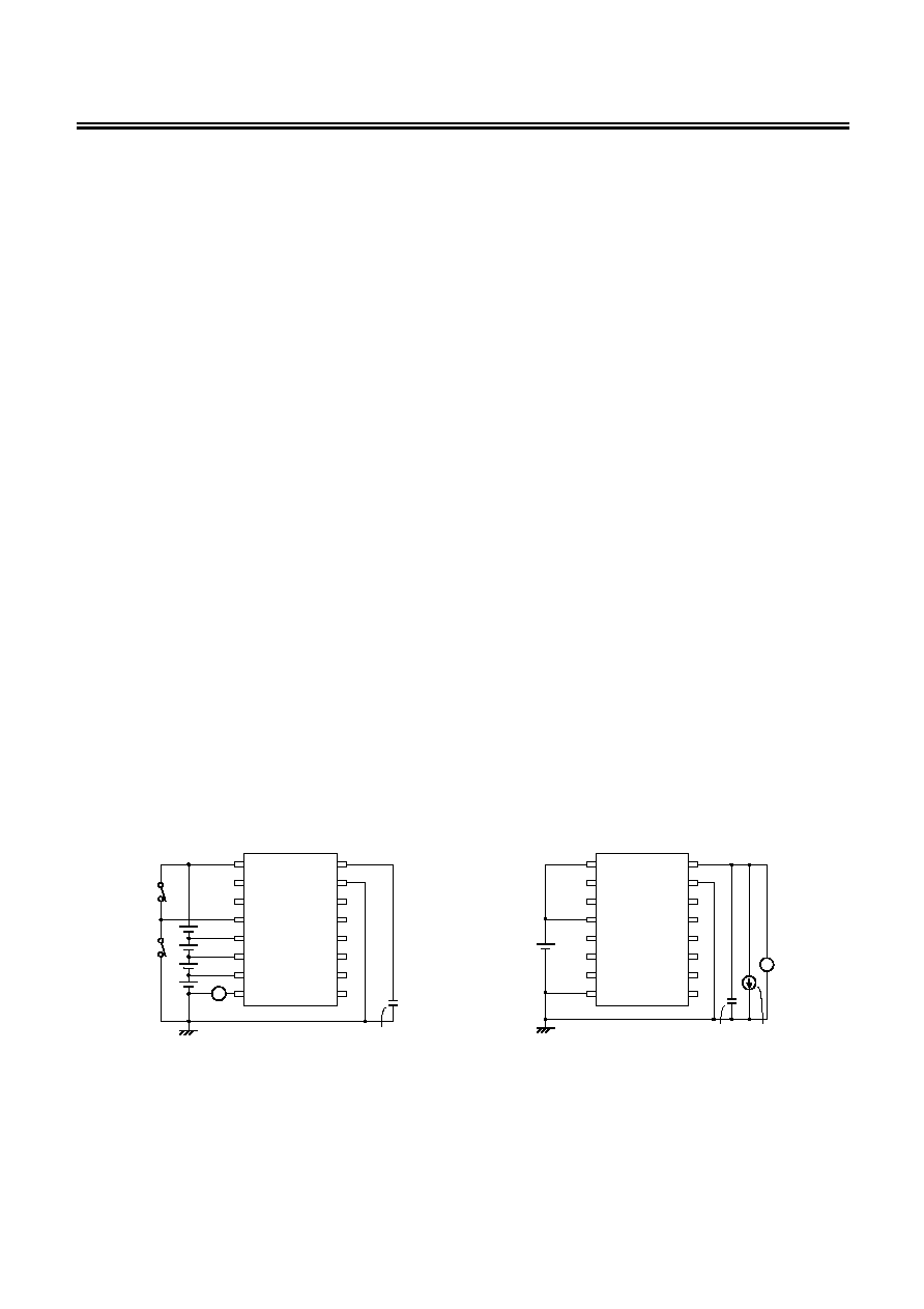
Test Circuits
In this chapter test methods are explained for the case of S-8243B series, which is designed for 4-serial cell
pack. For the case of S-8243A series, which is designed for 3-serial cell, voltage source V2 should be shorted,
V3 should be read as V2, and V4 as V3.
1. Current consumption (Test circuit 1)
Current consumption at not monitoring V
BATOUT
, I
OPE
, is a current measured at the VSS pin when V1
= V2
= V3 = V4 = 3.5 V and V
MP
= V
DD
. Current consumption at power down, I
PDN
, is a current measured at the
VSS pin when V1
= V2 = V3 = V4 = 1.5 V and V
MP
= V
SS
.
2. Voltage regulator (Test circuit 2)
Output voltage of the regulator V
OUT
is a voltage measured at the VREG pin when V
DD
= V
MP
= 14 V and
I
OUT
= 3 mA.
Line regulation of the voltage regulator
V
OUT1
is defined by the equation
V
OUT1
= V
OUT2
-V
OUT1
where
V
OUT1
is the output voltage when V
DD
= V
MP
= 6 V and I
OUT
= 3 mA, and V
OUT2
is the output voltage when V
DD
= V
MP
= 18 V and I
OUT
= 3 mA.
Load regulation of the regulator is defined by the equation
V
OUT2
= V
OUT3
-V
OUT
where V
OUT3
is the output
voltage when V
DD
= V
MP
= 14 V and I
OUT
= 5 ĶA.
3. Battery monitor amp and pin current for VC1 to VC3 (Test circuit 3)
Voltage gain of the battery monitor amp for each cell is defined by the input offset voltage and the
measurement result provided from the VBATOUT pin for the combination of the CTL3 pin and CTL4 pin
expressed by the following table at the condition where V1
= V2 = V3 = V4 = 3.5 V. Pin current for VC1 to
VC3, I
VCn
and I
VCnN
are at the same time measured.
Table 8
CTL3 pin status CTL4 pin status VBATOUT pin output VCn (n
=1, 2, 3) pin current
V
CTL3H
min.
V
CTL4H
min.
V
OFF1
I
VC1
at VC1 pin
V
CTL3H
min.
Open
V
BAT1
V
CTL3H
min.
V
CTL4L
max.
V
OFF2
I
VC2
at VC2 pin
Open V
CTL4H
min.
V
BAT2
Open Open
V
OFF3
I
VC3
at VC3 pin
Open V
CTL4L
max.
V
BAT3
V
CTL3L
max.
V
CTL4H
min.
V
OFF4
I
VCnN
at VCn pin (n
=1, 2, 3)
V
CTL3L
max.
Open
V
BAT4
Voltage gain of the battery monitor amp for each cell is calculated by the equation
GAMPn
= (V
BATn
-V
OFFn
) / Vn (n
= 1 to 4)
4. Overcharge detection voltages, overcharge detection hysteresis, overdischarge detection
voltages, overdischarge detection hysteresis, and overcurrent detection voltages (Test circuit 4)
Overcharge detection voltages, hysteresis voltages, and overdischarge detection voltages
In the following V
MP
=
V
DD
and the CDT pin is open.
The COP pin and the DOP pin should provide "Low", which is a voltage equal to V
DD
◊ 0.1 V or lower,
in the condition that V1
=
V2
=
V3
=
V4
=
3.5 V.
The overcharge detection voltage V
CU1
is defined by the voltage at which COP pin voltage becomes
"High", which is a voltage equal to VDD
◊ 0.9 V or higher, when the voltage V1 is gradually increased
from the starting condition V1
=
3.5 V. The overcharge release voltage V
CL1
is defined by the voltage
at which COP pin voltage becomes "Low" when the voltage V1 is gradually decreased. The hysteresis
voltage of the overcharge detection V
HC1
is then defined by the difference between the overcharge
detection voltage V
CU1
and the overcharge release voltage V
CL1
.

BATTERY PROTECTION IC FOR 3-SERIAL OR 4-SERIAL PACK
Rev.1.1
_00
S-8243A/B Series
Seiko Instruments Inc.
11
The overdischarge detection voltage V
DL1
is defined by the voltage at which DOP pin voltage becomes
"High" when the voltage V1 is gradually decreased from the starting condition V1
=
3.5 V. The
overdischarge release voltage V
DU1
is defined by the voltage at which DOP pin voltage becomes "Low"
when the voltage V1 is gradually increased. The hysteresis of the overdischarge detection voltage
V
HD1
is then defined by the difference between the overdischarge release voltage V
DU1
and the
overdischarge detection voltage V
DL1
.
Other overcharge detection voltage V
CUn
, hysteresis voltage of overcharge detection V
HCn
,
overdischarge detection voltage V
DLn
, and hysteresis of the overdischarge detection voltage V
HDn
( for
n
=
2 to 4) are defined in the same manner as in the case for n
=
1.
Overcurrent detection voltages
Starting condition is V1
=
V2
=
V3
=
V4
=
3.5 V, V
MP
=
V
DD
, and the CDT pin is open. The DOP pin
voltage thus provides "Low"
The overcurrent detection voltage 1, V
IOV1
is defined by the voltage difference V
DD
- V
MP
at which the
DOP pin voltage becomes "High" when the voltage of VMP pin is decreased.
Starting condition for measuring the overcurrent detection voltage 2 and 3 is V1
=
V2
=
V3
=
V4
=
3.5 V,
V
MP
=
V
DD
and the CDT pin voltage V
CDT
=
V
SS
. The DOP pin voltage thus provides "Low".
The overcurrent detection voltage 2, V
IOV2
is defined by the voltage difference V
DD
-V
MP
at which the
DOP pin voltage becomes "High" when the voltage of VMP pin is decreased.
The overcurrent detection delay time 2, t
IOV2
is a time needed for the DOP pin to become "High" from
"Low" when the VM pin voltage is changed quickly to V
IOV2
min.
-0.2 V from the starting condition V
MP
=
V
DD
.
The overcurrent detection voltage 3, V
IOV3
is defined by the voltage of the VM pin at which the DOP pin
voltage becomes "High" when the voltage of VMP pin is decreased at the speed 10 V / ms.
The overcurrent detection delay time 3, t
IOV3
is a time needed for the DOP pin to become "High" from
"Low" when the VM pin voltage is changed quickly to V
IOV3
min.
-0.2 V from the starting condition V
MP
=
V
DD
.
5. CTL1 pin current, overcharge detection delay, overdischarge detection delay, and overcurrent
detection delay 1 (Test circuit 5)
Starting condition is V1
=
V2
=
V3
=
V4
=
3.5 V and V
MP
=
V
DD
.
Current that flows between the CTL1 pin and V
SS
is the CTL1 pin current I
CTL1L
.
The overcharge detection delay time t
CU
is a time needed for the COP pin voltage to change from "Low" to
"High" just after the V1 voltage is rapidly increased from 3.5 V to 4.5 V.
The overdischarge detection delay time t
DL
is a time needed for the DOP pin voltage to change from "Low"
to "High" just after the V1 voltage is rapidly decreased from 3.5 V to 1.5 V.
The overcurrent detection delay time 1 is a time needed for the DOP pin voltage to change from "Low" to
"High" just after the VMP pin voltage is decreased from V
DD
to V
DD
-0.35 V when V1
=
3.5 V.
6. Input voltages for CTL1 and CTL2 (Test circuit 6)
Starting condition is V1
=
V2
=
V3
=
V4
=
3.5 V.
Pin voltages of the COP and the DOP should be "High" when V
CTL1
=
V
CTL1H
min. and CTL2 is OPEN.
Pin voltages of the COP and the DOP should be "Low" when V
CTL1
=
V
CTL1L
max. and CTL2 is OPEN.
Pin voltage of the COP is "High" and the pin voltage of the DOP is "Low" when V
CTL1
=
V
CTL1L
max. and
V
CTL2
=
V
CTL2H
min.
Pin voltage of the COP is "Low" and the pin voltage of the DOP is "High" when V
CTL1
=
V
CTL1L
max. and
V
CTL2
=
V
CTL2L
max.
BATTERY PROTECTION IC FOR 3-SERIAL OR 4-SERIAL PACK
S-8243A/B Series
Rev.1.1
_00
12
Seiko Instruments Inc.
7. 0 V battery charge starting charger voltage and 0 V battery charge inhibition battery voltage (Test
circuit 7)
One of the 0 V battery charge starting charger voltage and 0 V battery charge inhibition battery voltage is
applied to each product according to the 0V battery charging function.
Starting condition is V1
=
V2
=
V3
=
V4
=
0 V for a product in which 0 V battery charging is available.
The COP pin voltage should be lower than V
0CHA
max.
-1 V when the VMP pin voltage V
MP
=
V
0CHA
max.
Starting condition is V1
=
V2
=
V3
=
V4
=
V
0INH
for a product in which 0 V battery charging is inhibited.
The COP pin voltage should be higher than V
MP
-1 V when the VMP pin voltage V
MP
=
24 V.
8. Internal resistance (Test circuit 8)
The resistance between VDD and VMP is R
VDM
and is calculated by the equation R
VDM
=
V
DD
/ I
VDM
where
I
VDM
is a VMP pin current after V
MP
is changed to V
SS
from the starting condition V1
=
V2
=
V3
=
V4
=
3.5 V
and V
MP
=
V
DD
.
The resistance between VSS and VMP is R
VSM
and is calculated by the equation R
VSM
=
V
DD
/ I
VSM
where
I
VSM
is a VMP pin current at the condition V1
=
V2
=
V3
=
V4
=
1.8 V and V
MP
=
V
DD
.
9. Pin current for CTL2 to CTL4, COP, DOP, VBATOUT (Test circuit 9)
Starting condition is V1
=
V2
=
V3
=
V4
=
3.5 V.
Pin current for CTL2 at "High" is I
CTL2H
and is obtained by setting V
CTL2
=
V
OUT
.
Pin current for CTL2 at "Low" is I
CTL2L
and is obtained by setting V
CTL2
=
V
SS
.
Pin current for CTL3 and CTL4 can be obtained in the same manner as in the CTL2.
Pin current for COP at "High" is I
COH
and is obtained by setting V1
=
V2
=
V3
=
V4
=
6 V, V
MP
=
V
DD
, and V
COP
=
V
DD
. And pin current for COP at "Low" is I
COL
and is obtained by setting V1
=
V2
=
V3
=
V4
=
3.5 V, V
MP
=
V
DD
, and V
COP
=
0.5 V.
Pin current for DOP at "Low" is I
DOL
and is obtained by setting V1
=
V2
=
V3
=
V4
=
3.5 V, V
MP
=
V
DD
, and
V
DOP
=
0.5 V. And pin current for COP at "High" is I
COH
and is obtained by setting V1
=
V2
=
V3
=
V4
=
3.5
V, V
MP
=
V
DD
-1 V, and V
DOP
=
V
DD
-0.5 V.
Pin current for VBATOUT at "High" is I
VBATH
and is obtained by setting CTL3 and CTL4 are open and
V
BATOUT
=
V
OFF3
-0.5 V. And pin current for VBATOUT at "Low" is I
VBATL
and is obtained by setting V
BATOUT
=
V
OFF3
+0.5 V.
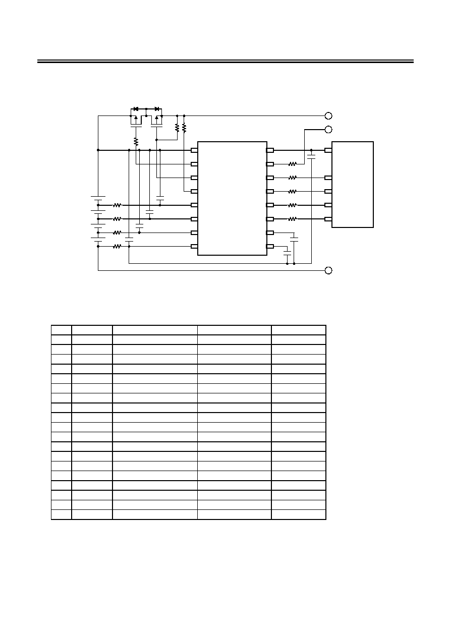
C1
=1 ĶF
V4
V3
V2
V1
8 VSS
7
VC3
6 VC2
5 VC1
3
COP
2 DOP
4 VMP
1
VDD
VBATOUT
11
VREG 16
CDT
9
CCT
10
CTL4
12
CTL2
14
CTL1 15
CTL3
13
A
C1
=1 ĶF
I
OUT
V
8 VSS
7
VC3
6 VC2
5 VC1
3
COP
2 DOP
4 VMP
1
VDD
VBATOUT
11
VREG 16
CDT
9
CCT
10
CTL4
12
CTL2
14
CTL1 15
CTL3
13
Test circuit 1
Test circuit 2
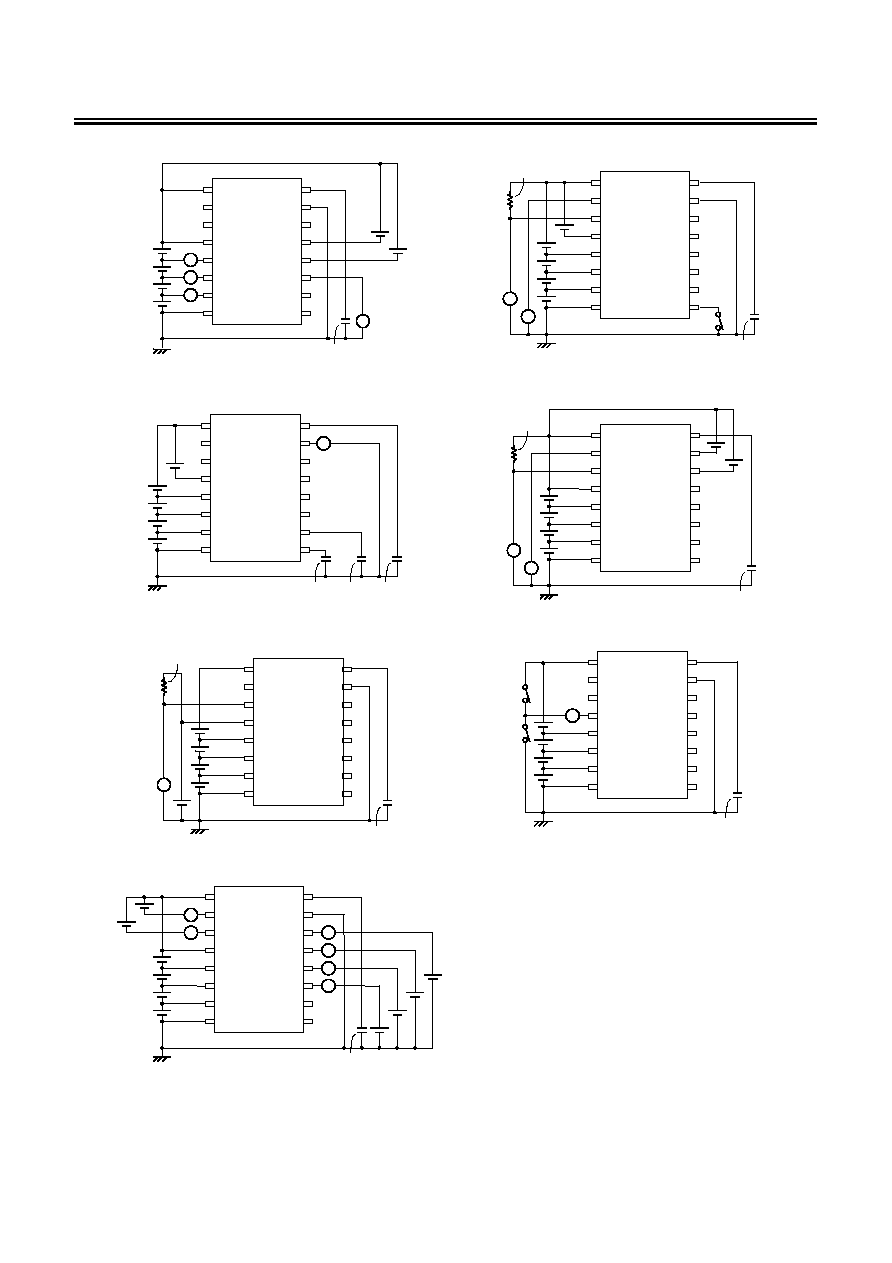
BATTERY PROTECTION IC FOR 3-SERIAL OR 4-SERIAL PACK
Rev.1.1
_00
S-8243A/B Series
Seiko Instruments Inc.
13
C1
=1 ĶF
V4
V3
V2
V1
V
A
A
A
8 VSS
7
VC3
6 VC2
5 VC1
3
COP
2 DOP
4 VMP
1
VDD
VBATOUT
11
VREG 16
CDT
9
CCT
10
CTL4
12
CTL2
14
CTL1 15
CTL3
13
R1
=1 M
V4
V3
V2
V1
V
V
C1
=1 ĶF
8 VSS
7
VC3
6 VC2
5 VC1
3
COP
2 DOP
4 VMP
1
VDD
VBATOUT
11
VREG 16
CDT
9
CCT
10
CTL4
12
CTL2
14
CTL1 15
CTL3
13
Test circuit 3
Test circuit 4
C2
=0.1 ĶF
V4
V3
V2
V1
A
C1
=1 ĶF
C3
=0.1 ĶF
8 VSS
7
VC3
6 VC2
5 VC1
3
COP
2 DOP
4 VMP
1
VDD
VBATOUT
11
VREG 16
CDT
9
CCT
10
CTL4
12
CTL2
14
CTL1 15
CTL3
13
C1
=1 ĶF
V4
V3
V2
V1
R1
=1 M
V
V
8 VSS
7
VC3
6 VC2
5 VC1
3
COP
2 DOP
4 VMP
1
VDD
VBATOUT
11
VREG 16
CDT
9
CCT
10
CTL4
12
CTL2
14
CTL1 15
CTL3
13
Test circuit 5
Test circuit 6
V4
V3
V2
V1
R1
=1 M
V
C1
=1 ĶF
8 VSS
7
VC3
6 VC2
5 VC1
3
COP
2 DOP
4 VMP
1
VDD
VBATOUT
11
VREG 16
CDT
9
CCT
10
CTL4
12
CTL2
14
CTL1 15
CTL3
13
V4
V3
V2
V1
A
C1
=1 ĶF
8 VSS
7
VC3
6 VC2
5 VC1
3
COP
2 DOP
4 VMP
1
VDD
VBATOUT
11
VREG 16
CDT
9
CCT
10
CTL4
12
CTL2
14
CTL1 15
CTL3
13
Test circuit 7
Test circuit 8
V4
V3
V2
V1
A
A
A
A
A
A
C1
=1 ĶF
8 VSS
7
VC3
6 VC2
5 VC1
3
COP
2 DOP
4 VMP
1
VDD
VBATOUT
11
VREG 16
CDT
9
CCT
10
CTL4
12
CTL2
14
CTL1 15
CTL3
13
Test circuit 9
Figure 4

BATTERY PROTECTION IC FOR 3-SERIAL OR 4-SERIAL PACK
S-8243A/B Series
Rev.1.1
_00
14
Seiko Instruments Inc.
Operation Descriptions
1. Battery protection circuit
Battery protection protects batteries from overcharge and overdischarge, and also protects external FETs
from overcurrent.
1-1 Normal condition
When all of the battery voltages are in the range from V
DLn
to V
CUn
and the discharge current is lower
than a specified value (the VMP pin voltage is lower than V
IOV1
), the charging and discharging FETs
are turned on.
1-2 Overcharge condition
When any one of the battery voltages becomes higher than V
CUn
and the state continues for t
CU
or
longer, the COP pin becomes high impedance and is pulled up to EB
+ pin voltage by an external
resistor, and the charging FET is turned off to stop charging. The overcharge condition is released
when one of the following two conditions holds.
a) All battery voltages become lower than V
CUn
+ V
HCn
.
b) V
DD
-V
MP
>V
IOV1
(A load is connected, and discharging starts.)
1-3 Overdischarge condition
When any one of the battery voltages becomes lower than V
DLn
and the state continues for t
DL
or
longer, the DOP pin voltage becomes V
DD
level, and the discharging FET is turned off to stop
discharging. After discharging is stopped due to overdischarge condition, the S-8243 enters power
down condition.
1-4 Power down condition
After stopping discharging due to overdischarge condition, the S-8243 enters power down condition.
In this condition, almost all circuits of the S-8243 are stopped to save current consumption. The
current consumption becomes lower than I
PDN
. In the power down condition, the VMP pin is pulled
down to V
SS
level by the internal R
VSM
resistor. In power down condition, output pin voltages are fixed
at the following levels.
a) COP
V
SS
(Charging FET is turned on)
b) DOP
V
DD
(Discharging FET is turned off)
c) VREG
V
SS
(Voltage regulator circuit is off)
d) VBATOUT V
SS
(Battery voltage monitor amp circuit is off)
The power down condition is released when the following condition holds.
a) V
MP
>V
IOV3
(A charger is connected, and charging starts.
)
The overdischarging status is released when the following condition holds.
a) All of the battery voltages are V
DLn
or higher, and the VDD pin voltage is V
DD
/2 or higher. (A
charger is connected.)
1-5 Overcurrent condition
The S-8243 has three overcurrent detection levels (V
IOV1
, V
IOV2
and V
IOV3
) and three overcurrent
detection delay times (t
IOV1
, t
IOV2
and t
IOV3
) corresponding to each overcurrent detection levels. When
the discharging current becomes higher than a specified value (the voltage between V
DD
and V
MP
is
greater than V
IOV1
) and the state continues for t
IOV1
or longer, the S-8243 enters the overcurrent
condition in which the DOP pin voltage becomes V
DD
level to turn off the discharging FET to stop
discharging, the COP pin becomes high impedance and is pulled up to EB
+ pin voltage by an external
resistor to turn off the charging FET to stop charging, and the VMP pin is pulled up to V
DD
voltage by
the internal resistor R
VDM
. Operation of two other overcurrent detection levels (V
IOV2
and V
IOV3
) and
overcurrent detection delay times (t
IOV2
and t
IOV3
) is the same as that for V
IOV1
and t
IOV1
.
The overcurrent condition is released when the following condition holds.
a) V
MP
>{V
IOV3
/ (1
-V
IOV3
)
◊ 3 / 5-2 / 5} ◊ R
VDM
(A load is released, and the impedance between the EB- and EB+ pin becomes higher.)

BATTERY PROTECTION IC FOR 3-SERIAL OR 4-SERIAL PACK
Rev.1.1
_00
S-8243A/B Series
Seiko Instruments Inc.
15
1-6 0 V battery charging function
Regarding the charging of a self-discharged battery (0 V battery) the S-8243 has two functions from
which one should be selected.
a) 0 V battery charging is allowed (0 V battery charging is available)
When a charger voltage is higher than V
0CHA
, 0 V battery can be charged.
b) 0 V battery charging is forbidden (0 V battery charging is impossible)
When one of the battery voltages is lower than V
0INH
, 0 V battery can not be charged.
Caution When the VDD pin voltage is lower than minimum of V
DSOP
, the operation of S-8243
series is not guaranteed.
1-7 Delay time setting
Overcharge detection delay times (t
CU1
to t
CU4
) are determined by the external capacitor at the CCT
pin. Overdischarge detection delay times (t
DL1
to t
DL4
) and overcurrent detection delay time 1 (t
IOV1
)
are determined by the external capacitor at CDT pin. Overcurrent detection delay time 2,3 (t
IOV2
, t
IOV3
)
are fixed internally.
S-8243AAC, AAD, AE, BAF
min. typ. max.
t
CU
[s]
= Delay factor ( 5 10 15
)◊C
CT
[
ĶF]
t
DL
[ms]
= Delay factor ( 500 1000 1500 )◊C
DT
[
ĶF]
t
IOV1
[ms]
= Delay factor ( 50 100 150
)◊C
DT
[
ĶF]
S-8243BAD
min. typ. max.
t
CU
[s]
= Delay factor ( 5 10 15
)◊C
CT
[
ĶF]
t
DL
[ms]
= Delay factor ( 555 1110 2220 )◊C
DT
[
ĶF]
t
IOV1
[ms]
= Delay factor ( 33.1 66.2 132 )◊C
DT
[
ĶF]
2. Voltage regulator circuit
Built-in voltage regulator can be used to drive a micro computer, etc. The voltage regulator supplies
voltage of 3.3 V (3 mA maximum) and an external capacitor is needed.
Caution In the power down condition the voltage regulator output is pulled down to the V
SS
level
by an internal resistor.
3. Battery monitor amp circuit
Battery monitor amp sends information of the batteries to a microcomputer. The battery monitor amp
output is controlled and selected by CTL3 and CTL4 pins to give the following two voltages.
a) V
BATn
=
GAMPn
◊ V
BATTERYn
+
V
OFFn
where GAMPn is the n-th voltage gain of the amp, V
BATTERYn
is
the n-th battery voltage, and V
OFFn
is the n-th offset voltage of the amp.
b) N-th offset voltage V
OFFn
Each battery voltage V
BATTERYn
(n
=
1 to 4) is thus calculated by following equation.
V
BATTERYn
=
{(V
BATn
- V
OFFn
} / GAMPn (n
=
1,2,3,4)
After the state of CTL3 and CTL4 are changed, a time between 25
Ķs and 250 Ķs is needed for the battery
monitor amp to become stable.
Caution In the power down condition the battery monitor amp output is the V
SS
level.
BATTERY PROTECTION IC FOR 3-SERIAL OR 4-SERIAL PACK
S-8243A/B Series
Rev.1.1
_00
16
Seiko Instruments Inc.
4. CTL pins
The S-8243 has four control pins. The CTL1 and CTL2 pins are used to control the COP and DOP pin
output voltages. CTL1 takes precedence over CTL2. CTL2 takes precedence over the battery protection
circuit. The CTL3 and CTL4 pins are used to control the VBATOUT pin output voltage.
Table 9 CTL1 and CTL2 Mode
Input Output
CTL1 pin
CTL2 pin
External discharging FET
External charging FET
High High
OFF
OFF
High Open
OFF
OFF
High Low
OFF
OFF
Open High
OFF
OFF
Open Open
OFF
OFF
Open Low
OFF
OFF
Low High
Normal
*1
OFF
*2
Low Open
Normal
*1
Normal
*1
Low Low
OFF
Normal
*1
*1. States are controlled by voltage detection circuit.
*2. Off state is brought after the overcharge detection delay time t
CU
.
Table 10 CTL3 and CTL4 Mode
Input Output
CTL3 pin
CTL4 pin
V
BATOUT
(A series)
V
BATOUT
(B series)
High
High
V1 Offset
V1 Offset
High Open V1
◊0.2 + V1 Offset
V1
◊0.2 + V1 Offset
High
Low
Don't use.
V2 Offset
Open High
Don't
use.
V2
◊0.2 + V2 Offset
Open
*1
Open
*1
V2 Offset
V3 Offset
Open Low V2
◊0.2 + V2 Offset
V3
◊0.2 + V3 Offset
Low
High
V3 Offset
V4 Offset
Low Open V3
◊0.2 + V3 Offset
V4
◊0.2 + V4 Offset
Low
Low
Don't use.
Don't use.
*1. CTL3 and CTL4 pins should be open when a microcomputer is not used.
BATTERY PROTECTION IC FOR 3-SERIAL OR 4-SERIAL PACK
Rev.1.1
_00
S-8243A/B Series
Seiko Instruments Inc.
17
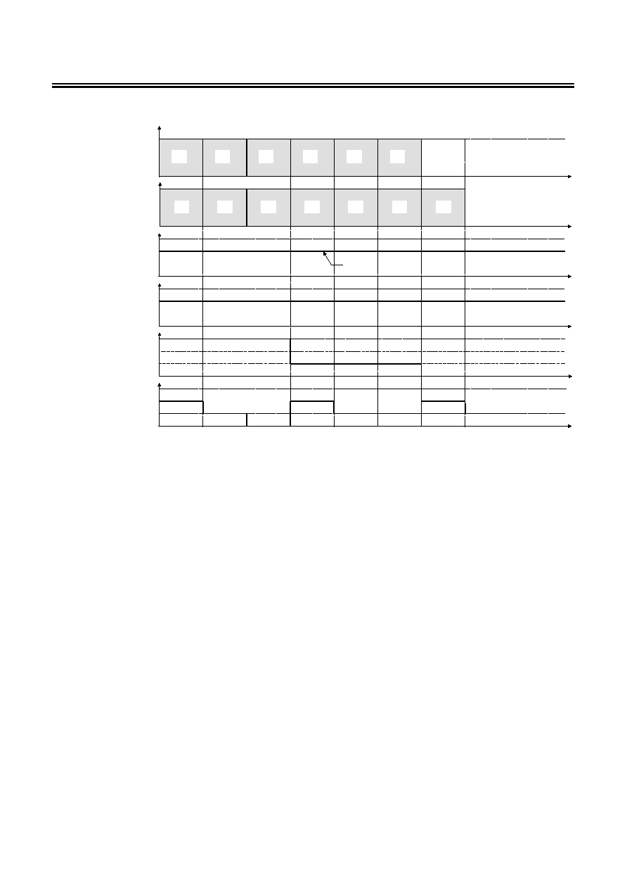
Operation Timing Charts
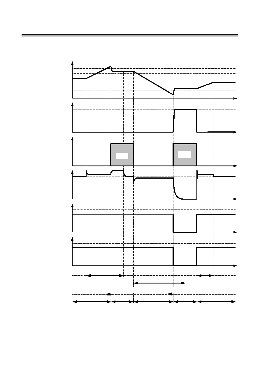
1. Overcharge detection, Over discharge detection
(n= 1~4)
V
CUn
V
DUn
V
DLn
V
CLn
Battery voltage
Hi-Z
V
DD
V
SS
COP pin voltage
V
IOV1
V
SS
VMP pin voltage
V
DD
V
DD
DOP pin voltage
V
SS
Charger connected
Load connected
Mode
*2
Overcharge detection delay time (t
CU
)
Overdischarge detection delay time (t
DL
)
V
BAT
V
SS
VBATOUT pin voltage
*1
V
OUT
V
OUT
V
SS
VREG pin votage
V
DD
Hi-Z
*1. State depends on CTL3 and CTL4 input levels. Refer to Figure.8
*2. : Normal mode, : Overcharge mode, : Overdischarge mode
Remark The charger is assumed to charge with a constant current. V
EB
+ indicates the open voltage of the
charger.
Figure 5
BATTERY PROTECTION IC FOR 3-SERIAL OR 4-SERIAL PACK
S-8243A/B Series
Rev.1.1
_00
18
Seiko Instruments Inc.
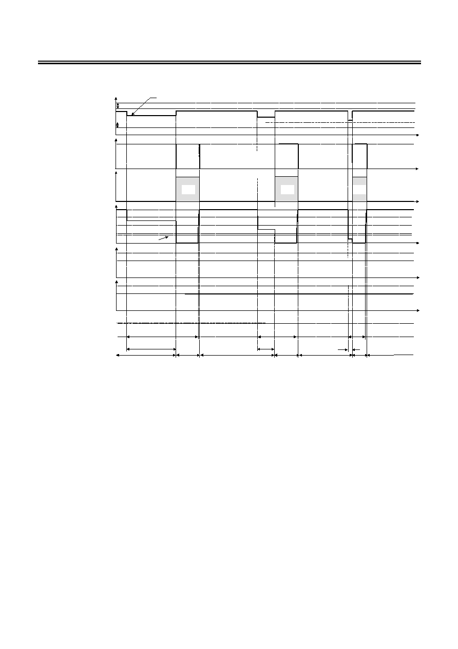
2. Overcurrent detection
V
CU
V
CL
V
DU
V
DL
Battery voltage
DOP pin voltage
V
DD
V
SS
V
return
*1
V
SS
V
DD
V
IOV1
V
IOV2
V
IOV3
V
SS
COP pin voltagae
VMP pin voltage
Charger connected
Delay Delay
Load connected
Mode
*3
Delay
V1,V2,V3 and V4 batteries
V
OUT
V
BAT
V
SS
V
DD
V
OUT
V
SS
VBATOUT pin voltage
*2
VREG pin voltage
Hi-z
Hi-z
Hi-z
V
HD
V
HC
*1. V
return
= V
DD
/ 6 (typ.)
*2. State depends on CTL3 and CTL4 input levels. Refer to Figure 8.
*3. : Normal mode, : Overcurrent mode
Remark The charger is assumed to charge with a constant current.
Figure 6
BATTERY PROTECTION IC FOR 3-SERIAL OR 4-SERIAL PACK
Rev.1.1
_00
S-8243A/B Series
Seiko Instruments Inc.
19
3. CTL1, CTL2 pin voltage
DOP pin voltage
V
DD
V
SS
V
SS
COP pin voltage
Hi-z
V
OUT
V
BAT
V
SS
V
DD
V
OUT
V
SS
VBATOUT pin voltage
VREG pin voltage
CTL1 pin voltage
CTL2 pin voltage
V
DD
V
OUT
OPEN
V
SS
V
DD
V
OUT
OPEN
V
SS
Hi-z
Hi-z
Hi-z
Hi-z
Hi-z
Hi-z
V
DD
V
DD
V
DD
V
DD
V
DD
V
DD
Normal
*1
V
DD
Normal
*1
Normal
*1
Normal
*1
(2)
*1. State depends on each battery voltage and the VMP pin voltage.
*2. State depends on CTL3 and CTL4 input levels. Refer to Figure 8.
Figure 7
BATTERY PROTECTION IC FOR 3-SERIAL OR 4-SERIAL PACK
S-8243A/B Series
Rev.1.1
_00
20
Seiko Instruments Inc.
4. CTL3, TL4 pin voltage
DOP pin voltage
*1
V
DD
V
SS
V
SS
COP pin voltage
*1
V
OUT
V
BAT
V
OFF
V
SS
V
DD
V
OUT
V
SS
VREG pin voltage
CTL3 pin voltage
CTL4 pin voltage
V
DD
V
OUT
OPEN
V
SS
V
DD
V
OUT
OPEN
V
SS
(1)
V
OUT
V
BAT
V
OFF
V
SS
Don't
use.
Don't
use.
Don't
use.
Don't
use.
V1 offset
V2 offset
V2 offset
V3 offset
V3 offset
V4 offset
V1 offset
V1
◊0.2
+V1 offset
B series 4-serial cell
VBATOUT pin voltage
A series 3-serial cell
VBATOUT pin voltage
(1)
(1)
(1)
(1)
(1)
(1)
(1) (1)
(1)
(1)
(1)
(1)
(1)
(1)
(1)
(1) (1)
V2
◊0.2
+V2 offset
V1
◊0.2
+V1 offset
V2
◊0.2
+V2 offset
V3
◊0.2
+V3 offset
V3
◊0.2
+V3 offset
V4
◊0.2
+V4 offset
*1. State depends on CTL1 and CTL2 and each battery voltage and the VMP pin voltage. Refer to Figures 5
to 7.
Figure 8

BATTERY PROTECTION IC FOR 3-SERIAL OR 4-SERIAL PACK
Rev.1.1
_00
S-8243A/B Series
Seiko Instruments Inc.
21
Standard Circuits
1. S-8243A Series
R
VSS
CTL1
R
VMP
R
DOP
EB-
EB+
8 VSS
7 VC3
6 VC2
5 VC1
3 COP
2 DOP
4 VMP
1 VDD
VBATOUT 11
CTL4 12
VREG 16
CCT 10
CTL2 14
CTL1 15
CTL3 13
CDT 9
C
VC3
C
VC2
S-8243A
C
VSS
R
VC3
R
VC2
Microcomputer
C
CDT
C
CCT
C
VREG
R
VBAT
R
CTL4
R
CTL3
R
CTL2
R
CTL1
Charging FET
Discharging FET
R
COP
Figure 10
Table 11 Recommended value for external parts
No. Part Recommended
value
Range
unit
1 R
VC2
1
0 to 1
k
2 R
VC3
1
0 to 1
k
3 R
VSS
10
0 to 10
4 R
DOP
5.1
2 to 10
k
5 R
COP
1
0.1 to 1
M
6 R
VMP
5.1
1 to 10
k
7 R
CTL1
0
0 to 100
k
8 R
CTL2
0
0 to 10
k
9 R
CTL3
0
0 to 10
k
10 R
CTL4
0
0 to 10
k
11 R
VBAT
0
0 to 100
k
12 C
VC2
0.047
0 to 0.22
ĶF
13 C
VC3
0.047
0 to 0.22
ĶF
14 C
VSS
4.7
0 to 10
ĶF
15 C
CCT
0.1
More than 0.01
ĶF
16 C
CDT
0.1
More than 0.02
ĶF
17 C
VREG
4.7
0.68 to 10
ĶF
Caution No resistance should be inserted in the power supply pin VDD.
Standard circuit does not guarantee proper operations. Evaluation
in actual application is needed to determine proper constants.
BATTERY PROTECTION IC FOR 3-SERIAL OR 4-SERIAL PACK
S-8243A/B Series
Rev.1.1
_00
22
Seiko Instruments Inc.
2. S-8243B Series
R
VSS
CTL1
Charging FET
Discharging FET
R
VMP
R
DOP
EB-
EB+
8 VSS
7 VC3
6 VC2
5 VC1
3 COP
2 DOP
4 VMP
1 VDD
VBATOUT 11
CTL4 12
VREG 16
CCT 10
CTL2 14
CTL1 15
CTL3 13
CDT 9
C
VC3
C
VC2
C
VC1
S-8243B
C
VSS
R
VC3
R
VC2
Microcomputer
C
CDT
C
CCT
C
VREG
R
VBAT
R
CTL4
R
CTL3
R
CTL2
R
CTL1
R
VC1
R
COP
Figure 11
Table 12 Recommended value for external parts
No. Part Recommended
value
Range
unit
1 R
VC1
1
0 to 1
k
2 R
VC2
1
0 to 1
k
3 R
VC3
1
0 to 1
k
4 R
VSS
10
0 to 10
5 R
DOP
5.1
2 to 10
k
6 R
COP
1
0.1 to 1
M
7 R
VMP
5.1
1 to 10
k
8 R
CTL1
0
0 to 100
k
9 R
CTL2
0
0 to 10
k
10 R
CTL3
0
0 to 10
k
11 R
CTL4
0
0 to 10
k
12 R
VBAT
0
0 to 100
k
13 C
VC1
0.047
0 to 0.22
ĶF
14 C
VC2
0.047
0 to 0.22
ĶF
15 C
VC3
0.047
0 to 0.22
ĶF
16 C
VSS
4.7
0 to 10
ĶF
17 C
CCT
0.1
More than 0.01
ĶF
18 C
CDT
0.1
More than 0.02
ĶF
19 C
VREG
4.7
0.68 to 10
ĶF
Caution No resistance should be inserted in the power supply pin VDD.
Standard circuit does not guarantee proper operations. Evaluation
in actual application is needed to determine proper constants.

BATTERY PROTECTION IC FOR 3-SERIAL OR 4-SERIAL PACK
Rev.1.1
_00
S-8243A/B Series
Seiko Instruments Inc.
23
Precautions
∑ Pay attention to the operating conditions for input/output voltage and load current so that the power loss in
the IC does not exceed the package power dissipation.
∑ Do not apply an electrostatic discharge to this IC that exceeds the performance ratings of the built-in
electrostatic protection circuit.
∑ Seiko Instruments Inc. shall not be responsible for any patent infringement by products including the S-8243
series, the method of using the S-8243 series in such products, the product specifications or the country of
destination thereof.

BATTERY PROTECTION IC FOR 3-SERIAL OR 4-SERIAL PACK
S-8243A/B Series
Rev.1.1
_00
24
Seiko Instruments Inc.
Application Circuits
1. S-8243A Series
CTL1
EB
-
-
-
-
EB
+
+
+
+
8 VSS
7 VC3
6 VC2
5 VC1
3 COP
2 DOP
4 VMP
1 VDD
VBATOUT 11
CTL4 12
VREG 16
CCT 10
CTL2 14
CTL1 15
CTL3 13
CDT 9
S-8243A
VREG
SMBus
VREG
VREG
LED1
LED2
LED3
LED4
LED5
DISP
VOUT
ESCL
ESCD
SMBC
SMBD
HDQ
SR2
SR1
SRC
VSS
RB1
VT
THON
VCELL1
CTL4
CTL3
CTL2
REG
VCC
Bq2063
S-24C
GND
WP
A2
A1
A0
SDA
SCL
VCC
Figure 12
2. S-8243B Series
CTL1
EB-
EB+
8 VSS
7 VC3
6 VC2
5 VC1
3 COP
2 DOP
4 VMP
1 VDD
VBATOUT 11
CTL4 12
VREG 16
CCT 10
CTL2 14
CTL1 15
CTL3 13
CDT 9
S-8243B
VREG
SMBus
VREG
VREG
LED1
LED2
LED3
LED4
LED5
DISP
VOUT
ESCL
ESCD
SMBC
SMBD
HDQ
SR2
SR1
SRC
VSS
RB1
VT
THON
VCELL1
CTL4
CTL3
CTL2
REG
VCC
Bq2063
S-24C
GND
WP
A2
A1
A0
SDA
SCL
VCC
Figure 13
Caution The application circuits do not guarantee proper operations. Evaluation in actual application
is needed to determine proper constants.

BATTERY PROTECTION IC FOR 3-SERIAL OR 4-SERIAL PACK
Rev.1.1
_00
S-8243A/B Series
Seiko Instruments Inc.
25
Typical Characteristics (Typical data)
1. Current consumption
0
20
40
60
80
100
120
0 4 8 12
16 20 24
V
DD
(V)
I
OP
E
( Ķ
A)
S-8243BAF
I
OPE
- V
DD
0
20
40
60
80
100
120
-40 -20 0 20 40 60 80
Ta (įC)
I
O
PE
( Ķ
A)
S-8243BAF
I
OPE
- Temp
0.00
0.02
0.04
0.06
0.08
0.10
0 4 8 12 16 20 24
V
DD
(V)
I
PD
N
( Ķ
A)
S-8243BAF
I
PDN
- V
DD
0.00
0.02
0.04
0.06
0.08
0.10
-40 -20 0 20 40 60 80
Ta (įC)
I
PDN
( Ķ
A)
S-8243BAF
I
PDN
- Temp
2. Overcharge detection/release voltage, overdischarge detection/release voltage, overcurrent detection
voltages, and delay times
4.225
4.230
4.235
4.240
4.245
4.250
4.255
4.260
4.265
4.270
4.275
-40 -20 0 20 40 60 80
Ta
(įC)
V
CU
(V
)
S-8243BAF
V
CU
- Temp
3.95
3.97
3.99
4.01
4.03
4.05
-40 -20 0 20 40 60 80
Ta (įC)
V
CL
(V
)
S-8243BAF
V
CL
- Temp
2.300
2.325
2.350
2.375
2.400
2.425
2.450
2.475
2.500
-40 -20 0 20 40 60 80
Ta (įC)
V
DU
(V
)
S-8243BAF
V
DU
- Temp
2.32
2.34
2.36
2.38
2.40
2.42
2.44
2.46
2.48
-40 -20 0 20 40 60 80
Ta (įC)
V
DL
(V)
S-8243BAF
V
DL
- Temp
0.175
0.180
0.185
0.190
0.195
0.200
0.205
0.210
0.215
0.220
0.225
10 12 14 16
V
DD
(V)
V
IO
V
1
(V
)
S-8243BAF
V
IOV1
- V
DD
0.175
0.180
0.185
0.190
0.195
0.200
0.205
0.210
0.215
0.220
0.225
-40 -20 0 20 40 60 80
Ta (įC)
V
IO
V
1
(V
)
S-8243BAF
V
IOV1
- Temp
BATTERY PROTECTION IC FOR 3-SERIAL OR 4-SERIAL PACK
S-8243A/B Series
Rev.1.1
_00
26
Seiko Instruments Inc.
-0.60
-0.55
-0.50
-0.45
-0.40
10
12
14
16
V
DD
(V)
V
IO
V
2
(V)
S-8243BAF
V
IOV2
- V
DD
V
DD
Reference
-0.60
-0.55
-0.50
-0.45
-0.40
-40 -20 0 20 40 60 80
Ta (įC)
V
IO
V
2
(V)
S-8243BAF
V
IOV2
- Temp
V
DD
Reference
0.425
0.450
0.475
0.500
0.525
0.550
0.575
10
12
14
16
V
DD
(V)
V
IO
V
3
/V
DD
(
-
)
S-8243BAF
V
IOV3
- V
DD
0.425
0.450
0.475
0.500
0.525
0.550
0.575
-40 -20 0 20 40 60 80
Ta (įC)
V
IO
V
3
/V
DD
(
-
)
S-8243BAF
V
IOV3
- Temp
0
5
10
15
0
0.2
0.4
0.6
0.8
1
C
CT
(ĶF)
t
CU
(s
)
S-8243BAF
t
CU
- C
CT
0.0
0.5
1.0
1.5
2.0
2.5
-40 -20
0
20 40 60 80
Ta (įC)
t
CU
(s
)
S-8243BAF
t
CU
- Temp
C
CT
=0.1ĶF
0
500
1000
1500
0
0.2
0.4 0.6 0.8
1
C
DT
(ĶF)
t
DL
(m
s)
S-8243BAF
t
DL
- C
DT
0
50
100
150
200
250
-40 -20 0
20 40 60 80
Ta (įC)
t
DL
(V)
S-8243BAF
t
DL
- Temp
C
DT
=0.1ĶF
0
50
100
150
0
0.2
0.4
0.6
0.8
1
C
DT
(ĶF)
t
IO
V
1
(m
s)
S-8243BAF
t
IOV1
- C
DT
0
5
10
15
20
25
-40 -20 0 20 40 60 80
Ta (įC)
t
IO
V1
(m
s)
S-8243BAF
t
IOV1
- Temp
C
DT
=0.1 Ķ F
1.5
2.0
2.5
3.0
3.5
4.0
-40 -20 0 20 40 60 80
Ta (įC)
t
IO
V2
(m
s)
S-8243BAF
t
IOV2
-Temp
100
200
300
400
500
600
-40 -20 0 20 40 60 80
Ta (įC)
t
IO
V3
( Ķ
s)
S-8243BAF
t
IOV3
-Temp
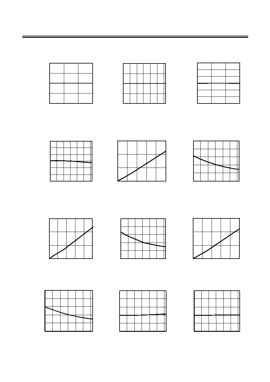
BATTERY PROTECTION IC FOR 3-SERIAL OR 4-SERIAL PACK
Rev.1.1
_00
S-8243A/B Series
Seiko Instruments Inc.
27
3. COP/DOP pin current
0.00
0.02
0.04
0.06
0.08
0.10
0 4 8 12 16 20 24
V
COP
(V)
I
COH
( Ķ
A
)
S-8243BAF
I
COH
- V
COP
0
5
10
15
20
25
30
35
40
0 3.5 7 10.5
14
V
COP
(V)
I
COL
(m
A
)
S-8243BAF
I
COL
- V
COP
-5
-4
-3
-2
-1
0
0 1.8 3.6 5.4 7.2
V
DOP
(V)
I
DO
H
(m
A
)
S-8243BAF
I
DOH
- V
DOP
0
5
10
15
20
25
30
35
40
0 3.5 7 10.5
14
V
DOP
(V)
I
DOL
(m
A
)
S-8243BAF
I
DOL
- V
DOP
4. Voltage regulator
3.0
3.1
3.2
3.3
3.4
3.5
3.6
-40 -20 0 20 40 60 80
Ta (įC)
V
OUT
(V)
S-8243BAF
V
OUT
- Temp
2.3
2.8
3.3
3.8
0 4 8 12 16
20 24
V
DD
(V)
V
OU
T
(V
)
S-8243BAF
V
OUT
- V
DD
V
DD
=0 24V, Ta=25įC
I
OUT
= 5
ĶA
100
ĶA
3mA
10mA
0.0
1.0
2.0
3.0
4.0
0 20 40 60 80 100
I
OUT
(mA)
V
OU
T
(V
)
S-8243BAF
V
OUT
- I
OUT
V1=V2=V3=V4=V
BAT
V
DD
=6V
14V
18V
10V
0.0
1.0
2.0
3.0
4.0
0
20
40
60
80
100
I
OUT
(mA)
V
OU
T
(V)
S-8243BAF
V
OUT
- I
OUT
85įC
Ta=-40įC
25įC
BATTERY PROTECTION IC FOR 3-SERIAL OR 4-SERIAL PACK
S-8243A/B Series
Rev.1.1
_00
28
Seiko Instruments Inc.
5. Battery monitor amp
150
155
160
165
170
175
180
1
2
3
4
5
V
BAT
(V)
V
OF
F
(m
V)
S-8243BAF
V
OFF
- V
BAT
V1=V2=V3=V4=V
BAT
V
OFF1
V
OFF2
V
OFF3
V
OFF4
150
155
160
165
170
175
180
-40 -20 0 20 40 60 80
Ta (įC)
V
OF
F
(m
V)
S-8243BAF
V
OFF
- Temp
V
OFF1
V
OFF2
V
OFF3
V
OFF4
0.198
0.199
0.200
0.201
0.202
1
2
3
4
5
V
BAT
(V)
GAM
P
(
-
)
S-8243BAF
GAMP - V
BAT
V1=V2=V3=V4=V
BAT
GAMP4
GAMP3
GAMP2
GAMP1
0.198
0.199
0.200
0.201
0.202
-40 -20 0 20 40 60 80
Ta
(įC)
GAM
P
(
-
)
S-8243BAF
GAMP
- Temp
GAMP1
GAMP2
GAMP3
GAMP4
0.17Ī0.05
9
1
8
16
5.1Ī0.2
0.22Ī0.08
0.65
No.
TITLE
SCALE
UNIT
mm
Seiko Instruments Inc.
No. FT016-A-P-SD-1.1
FT016-A-P-SD-1.1
TSSOP16-A-PKG Dimensions
4.0Ī0.1
2.0Ī0.1
Ý1.5
+0.1
-0
Ý1.6Ī0.1
8.0Ī0.1
4.2Ī0.2
6.5
+0.4
-0.2
0.3Ī0.05
1.5Ī0.1
(7.2)
No.
TITLE
SCALE
UNIT
mm
8
1
9
16
Seiko Instruments Inc.
No. FT016-A-C-SD-1.1
FT016-A-C-SD-1.1
TSSOP16-A-Carrier Tape
Feed direction
No.
TITLE
SCALE
UNIT
mm
17.4Ī1.0
21.4Ī1.0
17.4
+2.0
-1.5
2.0Ī0.5
Ý13.0Ī0.2
Ý21Ī0.8
Seiko Instruments Inc.
No. FT016-A-R-SD-1.1
FT016-A-R-SD-1.1
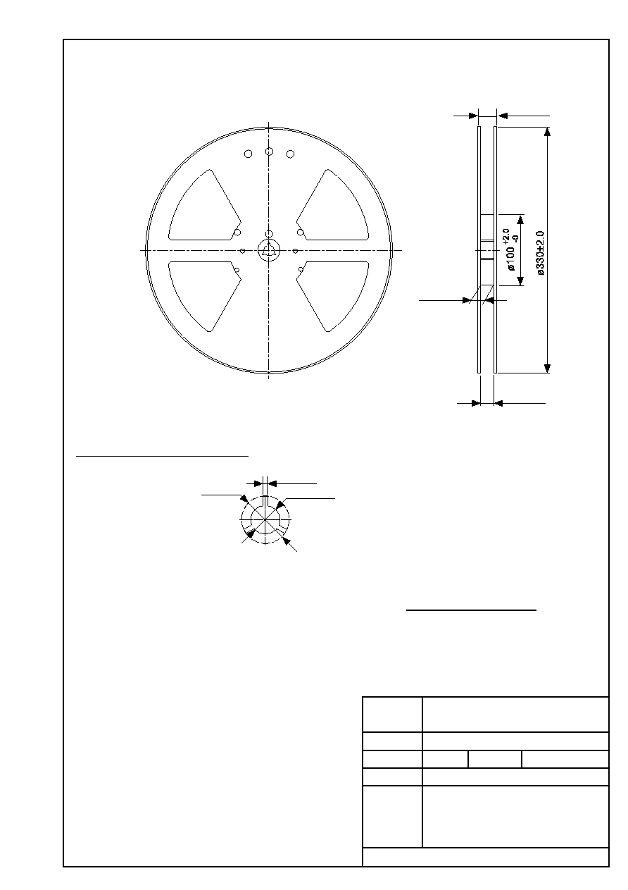
TSSOP16-A- Reel
Enlarged drawing in the central part
QTY.
2,000

∑
The information described herein is subject to change without notice.
∑
Seiko Instruments Inc. is not responsible for any problems caused by circuits or diagrams described herein
whose related industrial properties, patents, or other rights belong to third parties. The application circuit
examples explain typical applications of the products, and do not guarantee the success of any specific
mass-production design.
∑
When the products described herein are regulated products subject to the Wassenaar Arrangement or other
agreements, they may not be exported without authorization from the appropriate governmental authority.
∑
Use of the information described herein for other purposes and/or reproduction or copying without the
express permission of Seiko Instruments Inc. is strictly prohibited.
∑
The products described herein cannot be used as part of any device or equipment affecting the human
body, such as exercise equipment, medical equipment, security systems, gas equipment, or any apparatus
installed in airplanes and other vehicles, without prior written permission of Seiko Instruments Inc.
∑
Although Seiko Instruments Inc. exerts the greatest possible effort to ensure high quality and reliability, the
failure or malfunction of semiconductor products may occur. The user of these products should therefore
give thorough consideration to safety design, including redundancy, fire-prevention measures, and
malfunction prevention, to prevent any accidents, fires, or community damage that may ensue.