S8244_E1.3_00

Rev.1.3
_00
BATTRY PROTECTION IC FOR 1-SERIAL TO 4-SERIAL
(SECONDARY PROTECTION)
S-8244 Series
Seiko Instruments Inc.
1
The S-8244 Series is used for secondary protection of lithium-ion
batteries with from one to four cells, and incorporates a high-precision
voltage detector circuit and a delay circuit. Short-circuits between cells
accommodate series connection of one to four cells.
Features
· Internal high-precision voltage detector circuit
1) Overcharge detection voltage range:
3.70 to 4.50 V:
Accuracy of ± 25 mV (at +25
°C)
(at a 5 mV/step)
Accuracy of ± 50 mV (at -40 to +85
°C)
2) Hysteresis:
5 optional models available and selectable:
0.38±0.1 V, 0.25±0.07 V, 0.13±0.04 V, 0.045±0.02 V, None
· High withstand voltage device absolute maximum rating: 26 V
· Wide operating voltage range: 3.6 V to 24 V (refers to the range in which the delay circuit can
operate normally after overvoltage is detected)
· Delay time during detection:
Can be set by an external capacitor.
· Low current consumption
At 3.5 V for each cell: 3.0
µA max. (+25°C)
At 2.3 V for each cell: 2.4
µA max. (+25°C)
· Output logic and form - 4 types:
CMOS output active "H"
CMOS output active "L"
Pch open drain output active "L"
Nch open drain output active "H"
(only CMOS output for 0.045 V hysteresis models)
Applications
· Lithium ion rechargeable battery packs (secondary protection)
Package
· 8-Pin MSOP (Package drawing code: FN008-A)
BATTERY PROTECTION IC FOR 1-SERIAL TO 4-SERIAL (SECONDARY PROTECTION)
S-8244 Series
Rev.1.3_
00
2
Seiko Instruments Inc.
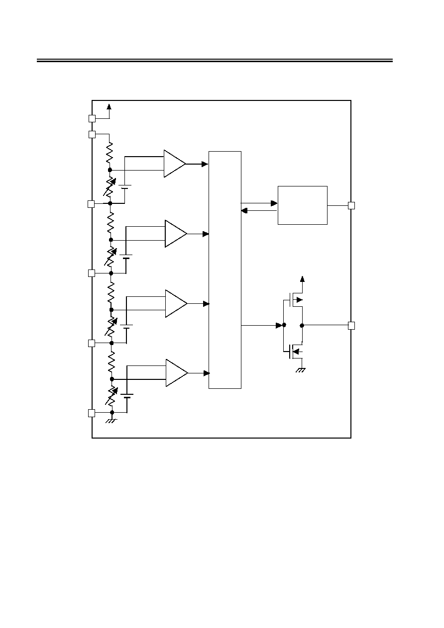
Block Diagram
VCC
ICT
VC2
VC1
-
+
CO
SENSE
VC3
Control
logic
Overcharge detection
comparator 4
Overcharge detection
comparator 3
Overcharge detection
comparator 2
Overcharge detection
comparator 1
Reference voltage 4
Reference voltage 3
Reference voltage 2
Reference voltage 1
VSS
-
+
-
+
-
+
Overcharge
detection
delay circuit
Note In the case of Nch open-drain output, only the Nch transistor will be
connected to the CO pin. In the case of Pch open-drain output, only
the Pch transistor will be connected to the CO pin.
Figure 1
BATTERY PROTECTION IC FOR 1-SERIAL TO 4-SERIAL (SECONDARY PROTECTION)
Rev.1.3
_00
S-8244 Series
Seiko Instruments Inc
3
Selection Guide
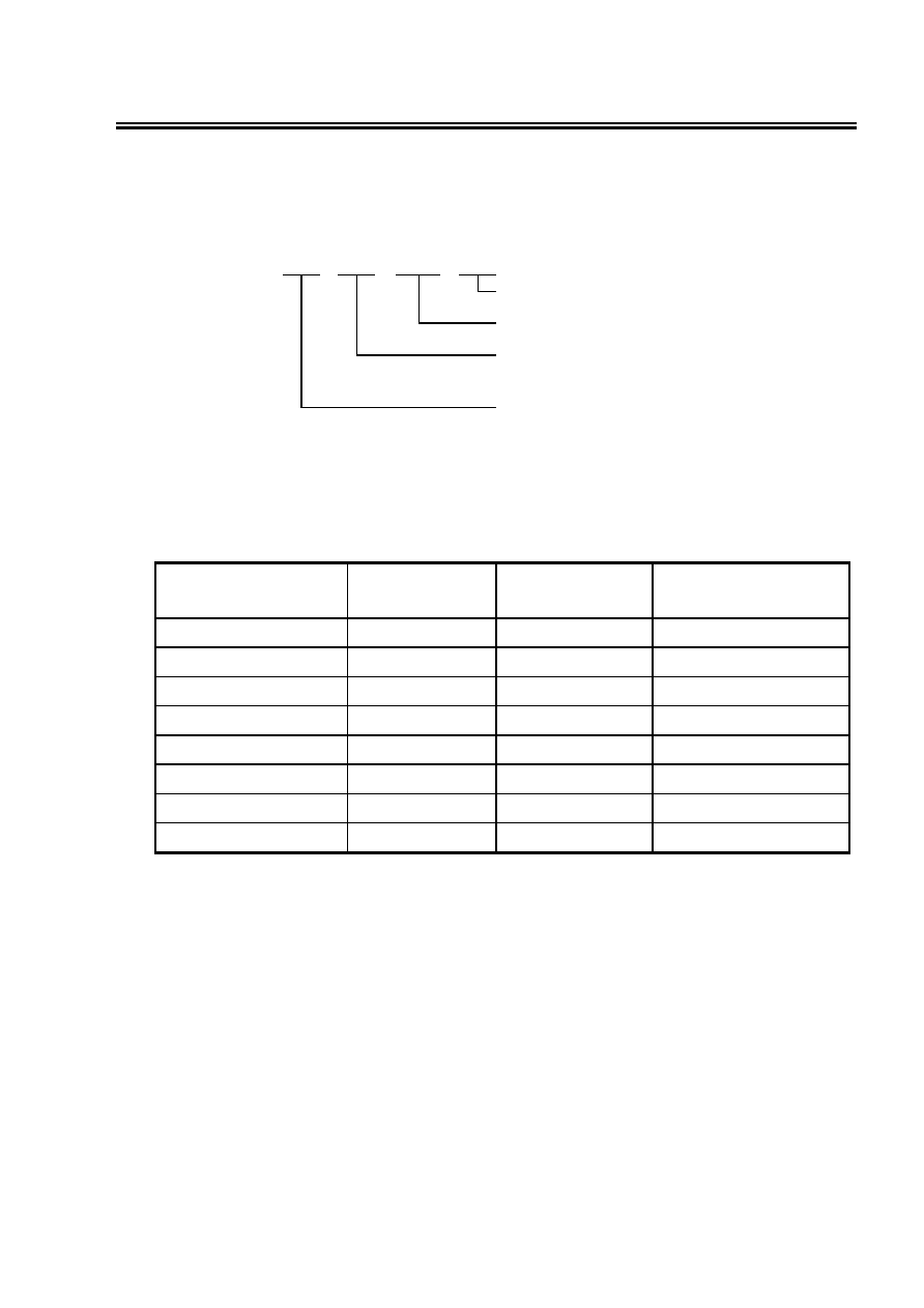
1. Product Name
S
-
-
-
-8244A xx FN ---- xxx ---- T2
IC direction of tape specifications
*1
Product name (abbrevation)
*2
Package abbreviation
FN: 8-Pin MSOP
Additional number
Sequentially set from AA to ZZ
*1. Refer to the taping drawing.
*2. Refer to the product name list.
2. Product Name List
Table 1
Model No./Item
Overcharge
detection voltage
V
CU
Overcharge
hysteresis voltage
V
CD
Output form
S-8244AAAFN-CEA-T2
4.45
± 0.025 V
0.38
± 0.1 V
CMOS output active "H"
S-8244AABFN-CEB-T2
4.2
± 0.025 V
0 V
Nch open drain active "H"
S-8244AACFN-CEC-T2
4.115
± 0.025 V
0.13
± 0.04 V
CMOS output active "H"
S-8244AADFN-CED-T2
4.2
± 0.025 V
0 V
Pch open drain active "L"
S-8244AAEFN-CEE-T2
4.225
± 0.025 V
0 V
Nch open drain active "H"
S-8244AAFFN-CEF-T2
4.35
± 0.025 V
0.045
± 0.02 V
CMOS output active "H"
S-8244AAGFN-CEG-T2
4.45
± 0.025 V
0.045
± 0.02 V
CMOS output active "H"
S-8244AAHFN-CEH-T2
4.30
± 0.025 V
0.25
± 0.07 V
CMOS output active "H"
Remark If a product with the required detection voltage does not appear in the above
list, contact our sales office.
BATTERY PROTECTION IC FOR 1-SERIAL TO 4-SERIAL (SECONDARY PROTECTION)
S-8244 Series
Rev.1.3_
00
4
Seiko Instruments Inc.
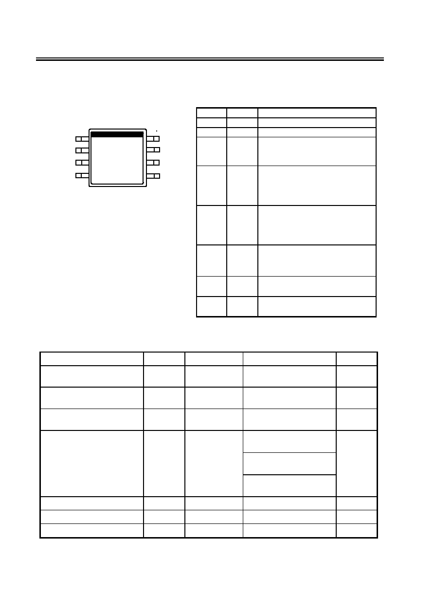
Pin Assignment
Table 2
Pin No. Symbol
Description
1 VCC
Positive power input pin
2 SENSE
Positive voltage connection pin of Battery 1
3 VC1
Negative voltage connection pin of
Battery 1;
Positive voltage connection pin of Battery 2
4 VC2
Negative voltage connection pin of
Battery 2;
Positive voltage connection pin of
Battery 3
8-Pin MSOP
Top view
3
2
4
1 8
6
7
5
VCC
SENSE
VC1
VC2
CO
ICT
VSS
VC3
Figure 2
5 VC3
Negative voltage connection pin of
Battery 3;
Positive voltage connection pin of
Battery 4
6 VSS
Negative power input pin;
Negative voltage connection pin of
Battery 4
7 ICT
Capacitor connection pin for
overcharge detection delay
8 CO
FET gate connection pin for charge
control
Absolute Maximum Ratings
Table 3
(Ta
= 25°C unless otherwise specified)
Item Symbol
Applicable
pin
Rating Unit
Input voltage between VCC
and VSS
V
DS
VCC V
SS
-0.3 to V
SS
+26
V
Delay capacitor connection
pin voltage
V
ICT
ICT V
SS
-0.3 to V
CC
+0.3
V
Input pin voltage
V
IN
SENSE, VC1,
VC2, VC3
V
SS
-0.3 to V
CC
+0.3
V
V
SS
-0.3 to V
CC
+0.3
(CMOS output)
CO output pin voltage
V
CO
CO
V
SS
-0.3 to 26
(Nch open drain output)
V
V
CC
-26 to V
CC
+0.3
(Pch open drain output)
Power dissipation
P
D
300 mW
Operating temperature range
T
opr
-40 to +85
°C
Storing temperature range
T
stg
-40 to +125
°C
Caution The absolute maximum ratings are rated values exceeding which the product could
suffer physical damage. These values must therefore not be exceeded under any
conditions.
BATTERY PROTECTION IC FOR 1-SERIAL TO 4-SERIAL (SECONDARY PROTECTION)
Rev.1.3
_00
S-8244 Series
Seiko Instruments Inc
5
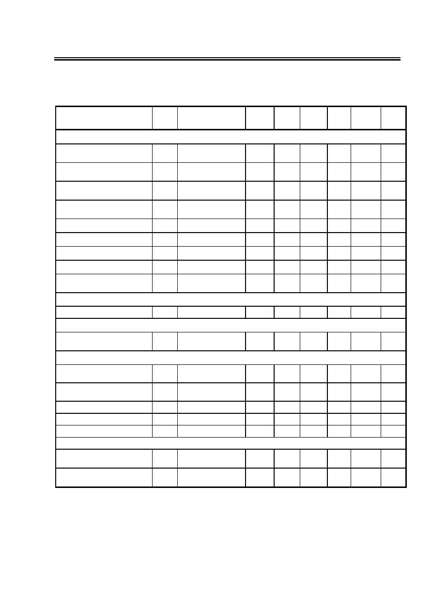
Electrical Characteristics
Table 4
(Ta
= 25
°C
unless otherwise specified)
Item Symbol
Conditions
Min.
Typ.
Max.
Unit
Measure-
ment
conditions
Measure
-ment
circuit
DETECTION VOLTAGE
Overcharge detection voltage 1
*1
V
CU1
3.7 to 4.5 V Adjustment
V
CU1
-0.025
V
CU1
V
CU1
+0.025
V 1 1
Overcharge detection voltage 2
*1
V
CU2
3.7 to 4.5 V Adjustment
V
CU2
-0.025
V
CU2
V
CU2
+0.025
V 2 1
Overcharge detection voltage 3
*1
V
CU3
3.7 to 4.5 V Adjustment
V
CU3
-0.025
V
CU3
V
CU3
+0.025
V 3 1
Overcharge detection voltage 4
*1
V
CU4
3.7 to 4.5 V Adjustment
V
CU4
-0.025
V
CU4
V
CU4
+0.025
V 4 1
Overcharge hysteresis voltage 1
*2
V
CD1
0.28 0.38 0.48 V
1
1
Overcharge hysteresis voltage 2
*2
V
CD2
0.28 0.38 0.48 V
2
1
Overcharge hysteresis voltage 3
*2
V
CD3
0.28 0.38 0.48 V
3
1
Overcharge hysteresis voltage 4
*2
V
CD4
0.28 0.38 0.48 V
4
1
Detection voltage temperature
coefficient
*3
T
COE
Ta
=-40 to 85°C
-0.4
0.0
+0.4 mV/°C
DELAY TIME
Overcharge detection delay time
t
CU
C
=0.1 µF
1.0 1.5 2.0 s 5 2
OPERATING VOLTAGE
Operating voltage between VCC
and VSS
*4
V
DSOP
3.6
24 V
CURRENT CONSUMPTION
Current consumption during
normal operation
I
OPE
V1
=V2=V3=V4=3.5V
1.5 3.0 µA
6 3
Current consumption at power
down
I
PDN
V1
=V2=V3=V4=2.3V
1.2 2.4 µA
6 3
VC1 sink current
I
VC1
V1
=V2=V3=V4=3.5V
-0.3
0.3
µA
6 3
VC2 sink current
I
VC2
V1
=V2=V3=V4=3.5V
-0.3
0.3
µA
6 3
VC3 sink current
I
VC
3
V1
=V2=V3=V4=3.5V
-0.3
0.3
µA
6 3
OUTPUT VOLTAGE
*5
CO "H" voltage
V
CO(H)
at I
OUT
= 10 µA
V
CC
-0.05
V 7 4
CO "L" voltage
V
CO(L)
at I
OUT
= 10 µA
V
SS
+0.05
V 7 4
*
1. ±50 mV when Ta
= -40 to +85°C.
*
2. 0.25±0.07 V, 0.13±0.04 V, 0.045±0.02 V except for 0.38 V hysteresis models.
*
3. Overcharge detection voltage or overcharge hysteresis voltage.
*
4. Operating voltage indicates that the delay circuit operates normally after an overcharge is detected.
*
5. Output logic and CMOS or open drain output can be selected.
Document Outline
- S-8244 Series
- Cover
- Features
- Applications
- Package
- Block Diagram
- Selection Guide
- Pin Assignment
- Absolute Maximum Ratings
- Electrical Characteristics
- Measurement Circuits
- Description of Operation
- Operation Timing Chart
- Battery Protection IC Connection Example 1
- Battery Protection IC Connection Example 2
- Battery Protection IC Connection Example 3 (for three cells)
- Battery Protection IC Connection Example 4 (for two cells)
- Battery Protection IC Connection Example 5 (for one cell)
- Precautions
- Characteristic (Typical Data)
- Package Drawing