 | –≠–ª–µ–∫—Ç—Ä–æ–Ω–Ω—ã–π –∫–æ–º–ø–æ–Ω–µ–Ω—Ç: S-8253BAA | –°–∫–∞—á–∞—Ç—å:  PDF PDF  ZIP ZIP |
Document Outline
- S-8253A/B Series
- Cover
- Features
- Applications
- Package
- Block Diagram
- Product Code Structure
- Pin Assignment
- Absolute Maximum Ratings
- Electrical Characteristics
- Test Circuits
- Description of Operation
- Operation Timing Chart
- Standard Circuit
- Precautions
- Characteristics (Typical Data)
- Package drawing

Rev.2.1
_00
BATTERY PROTECTION IC
FOR 2-SERIAL OR 3-SERIAL-CELL PACK
S-8253A/B Series
Seiko Instruments Inc.
1
The S-8253A/B Series are protection ICs for 2-serial or 3-serial cell
lithium-ion rechargeable batteries and include high-accuracy
voltage detectors and delay circuits.
These ICs are suitable for protecting lithium-ion battery packs from
overcharge, overdischarge and overcurrent.
Features
(1) High-accuracy voltage detection for each cell
∑ Overcharge detection voltage n (n = 1 to 3)
3.9 V to 4.4 V (50 mV steps) Accuracy
±25 mV
∑ Overcharge release voltage n (n = 1 to 3)
3.8 V to 4.4 V
*1
Accuracy
±50 mV
*1. Overcharge release voltage
= Overcharge detection voltage - Overcharge hysteresis voltage
(Overcharge hysteresis voltage n (n
= 1 to 3) can be selected as 0 V or from a range of 0.1 V to
0.4 V in 50 mV steps.)
∑ Overdischarge detection voltage n (n = 1 to 3) 2.0 V to 3.0 V (100 mV steps) Accuracy ±80 mV
∑ Overdischarge release voltage n (n = 1 to 3) 2.0 V to 3.4 V
*2
Accuracy
±100 mV
*2. Overdischarge release voltage
= Overdischarge release voltage - Overdischarge hysteresis
voltage
(Overdischarge hysteresis voltage n (n
= 1 to 3) can be selected as 0 V or from a range of 0.2 V to
0.7 V in 100 mV steps.)
(2) Three-level overcurrent detection (including load short circuiting detection)
∑ Overcurrent detection voltage 1
0.05 V to 0.30 V (50 mV steps) Accuracy
±25 mV
∑ Overcurrent detection voltage 2
0.5 V (fixed)
∑ Overcurrent detection voltage 3
1.2 V (fixed)
(3) Delay times (overcharge, overdischarge, overcurrent) are generated by an internal circuit (external
capacitors are unnecessary).
(4) Charge/discharge operation can be inhibited via the control pin.
(5) 0 V battery charge function available/unavailable are selectable.
(6) High-voltage withstand devices
Absolute maximum rating: 26 V
(7) Wide operating voltage range
2 V to 24 V
(8) Wide operating temperature range
-40∞C to +85 ∞C
(9) Low current consumption
∑ Operation mode
28
µA max. (+25∞C)
∑ Power-down mode
0.1
µA max. (+25∞C)
Applications
∑ Lithium-ion rechargeable battery packs
∑ Lithium polymer rechargeable battery packs
Package
∑ 8-Pin TSSOP (Package drawing code: FT008-D)
BATTERY PROTECTION IC FOR 2-SERIAL OR 3-SERIAL-CELL PACK
S-8253A/B Series
Rev.2.1
_00
Seiko Instruments Inc.
2
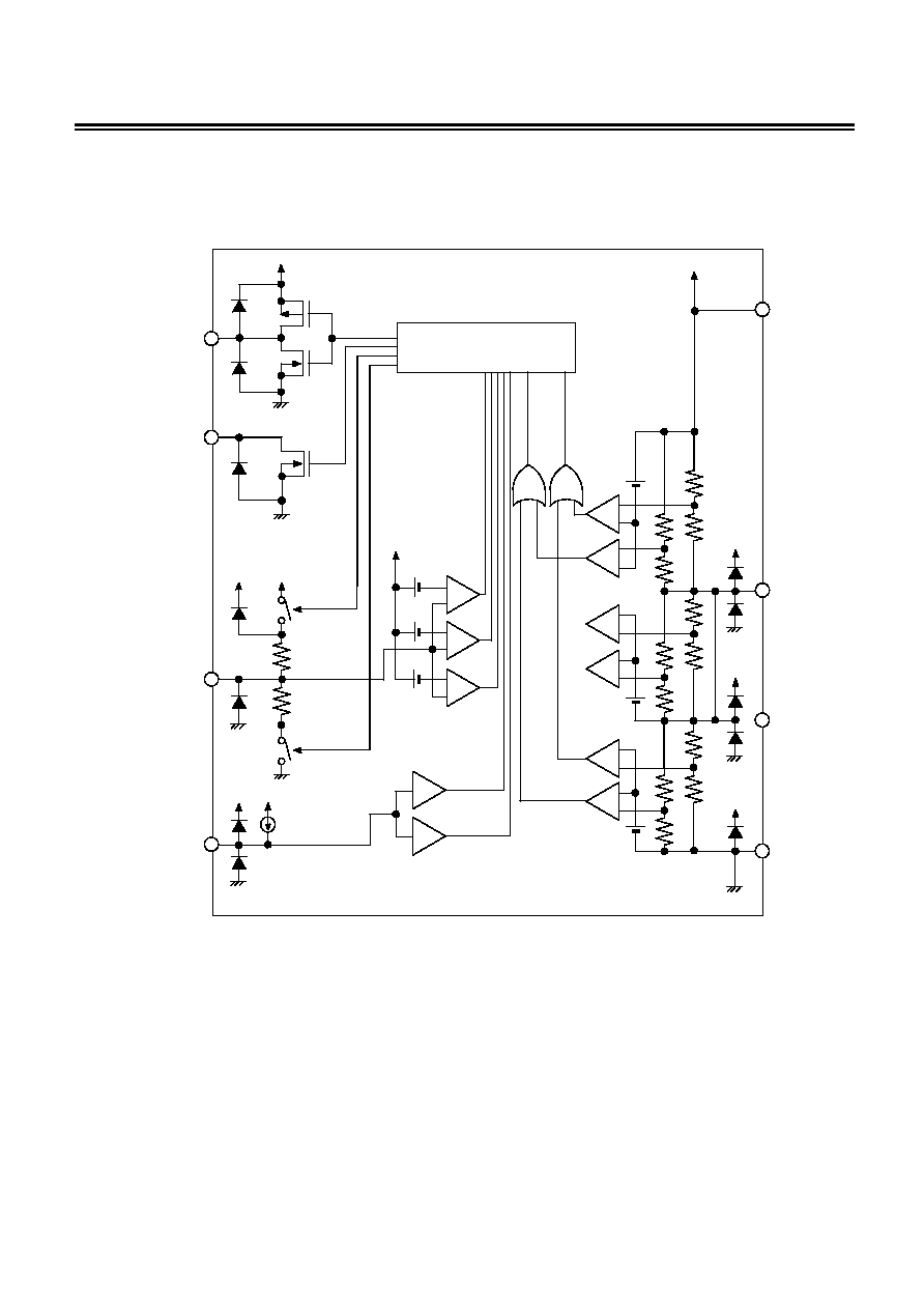
Block Diagram
(1) S-8253A Series
COP
VDD
DOP
VMP
95 k
900 k
+
-
+
-
+
-
Oscillator, counter,
controller
200 nA
CTL
CTLH
CTLM
VC1
-
+
+
-
-
+
+
-
-
+
+
-
VC2
VSS
Figure 1 Block Diagram (S-8253A Series)

BATTERY PROTECTION IC FOR 2-SERIAL OR 3-SERIAL-CELL PACK
Rev.2.1
_00
S-8253A/B Series
Seiko Instruments Inc.
3
(2) S-8253B Series
COP
VDD
DOP
VMP
95 k
900 k
+
-
+
-
+
-
Oscillator, counter,
controller
200 nA
CTL
CTLH
CTLM
VC1
-
+
+
-
-
+
+
-
-
+
+
-
VC2
VSS
Figure 2 Block Diagram (S-8253B Series)

BATTERY PROTECTION IC FOR 2-SERIAL OR 3-SERIAL-CELL PACK
S-8253A/B Series
Rev.2.1
_00
Seiko Instruments Inc.
4
Product Code Structure
1. Product Name
S
-
-
-
-8253
x xx
-
-
-
- T8T1
Indicates package type and packing specification of IC
*1
T8T1 : 8-Pin TSSOP
Additional number
Sequentially set from AA to ZZ
Product series
A: 2-cell
B:
3-cell
*1. Refer to the taping drawing.
2. Product Name List
Table 1 S-8253A Series (for 2-Serial Cell)
Product
Name/Parameter
Overcharge
Detection Voltage
V
CU
Overcharge
Release Voltage
V
CL
Overdischarge
Detection Voltage
V
DL
Overdischarge
Release Voltage
V
DU
Overcurrent
Detection Voltage 1
V
IOV1
0 V Battery
Charge
S-8253AAA-T8T1 4.35
± 0.025 V
4.05
± 0.050 V
2.40
± 0.080 V
2.70
± 0.100 V
0.30
± 0.025 V
Available
Remark If a product with the required detection voltage does not appear in the above list, contact our sales
office.
Table 2 S-8253B Series (for 3-Serial Cell)
Product
Name/Parameter
Overcharge
Detection Voltage
V
CU
Overcharge
Release Voltage
V
CL
Overdischarge
Detection Voltage
V
DL
Overdischarge
Release Voltage
V
DU
Overcurrent
Detection Voltage 1
V
IOV1
0 V Battery
Charge
S-8253BAA-T8T1 4.35
± 0.025 V
4.05
± 0.050 V
2.40
± 0.080 V
2.70
± 0.100 V
0.30
± 0.025 V
Available
Remark If a product with the required detection voltage does not appear in the above list, contact our sales
office.

BATTERY PROTECTION IC FOR 2-SERIAL OR 3-SERIAL-CELL PACK
Rev.2.1
_00
S-8253A/B Series
Seiko Instruments Inc.
5
Pin Assignment
8-Pin TSSOP
Top view
Table 3 S-8253A Series
Pin No.
Pin
Name
Function
1 DOP
Connection of discharge control FET gate
(CMOS output)
2 COP
Connection of charge control FET gate (Nch
open-drain output)
3 VMP
Voltage detection between VDD and VMP
(overcurrent detection pin)
4 CTL
Input of charge/discharge control signal, pin for
shortening test time
(L: Normal operation,
H: Charge/discharge inhibited,
M (V
DD
◊ 1/2): Test time reduced)
5 VSS
Negative power supply input, negative voltage
connection for battery 2
6 VC2
No connection
*1
7 VC1
Connection for negative voltage of battery 1 and
positive voltage of battery 2
8 VDD
Connection for positive power supply input and
positive voltage of battery 1
1
2
3
4
8
7
6
5
VDD
VC1
VC2
VSS
DOP
COP
CTL
VMP
Figure 3
*1. No connection is electrically open.
This pin can be connected to VDD or VSS.
Remark For the external views, refer to package drawings.
Table 4 S-8253B Series
Pin No.
Pin
Name
Function
1 DOP
Connection of discharge control FET gate
(CMOS output)
2 COP
Connection of charge control FET gate (Nch
open-drain output)
3 VMP
Voltage detection between VDD and VMP
(overcurrent detection pin)
4 CTL
Input of charge/discharge control signal, pin for
shortening test time
(L: Normal operation,
H: Charge/discharge inhibited,
M (V
DD
◊ 1/2): Test time reduced)
5 VSS
Connection for negative power supply input and
negative voltage of battery 3
6 VC2
Connection for negative voltage of battery 2 and
positive voltage of battery 3
7 VC1
Connection for negative voltage of battery 1 and
positive voltage of battery 2
8 VDD
Connection for positive power supply input and
positive voltage of battery 1
Remark For the external views, refer to package drawings.

BATTERY PROTECTION IC FOR 2-SERIAL OR 3-SERIAL-CELL PACK
S-8253A/B Series
Rev.2.1
_00
Seiko Instruments Inc.
6
Absolute Maximum Ratings
Table 5
(Ta
= 25∞C unless otherwise specified)
Parameter Symbol
Applicable
Pins Rating
Unit
Input voltage between VDD and
VSS
V
DS
V
SS
- 0.3 to V
SS
+ 26
V
Input pin voltage
V
IN
VC1, VC2
V
SS
- 0.3 to V
DD
+ 0.3
VMP pin input voltage
V
VMP
VMP
V
SS
- 0.3 to V
SS
+ 26
DOP pin output voltage
V
DOP
DOP
V
SS
- 0.3 to V
DD
+ 0.3
COP pin output voltage
V
COP
COP
V
SS
- 0.3 to V
VMP
+ 0.3
CTL input pin voltage
V
IN
_CTL
CTL
V
SS
- 0.3 to V
DD
+ 0.3
Power dissipation
P
D
300 mW
Operating temperature range
T
opr
-40 to +85
∞C
Storage temperature range
T
stg
-40 to +125
Caution The absolute maximum ratings are rated values exceeding which the product could suffer
physical damage. These values must therefore not be exceeded under any conditions.

BATTERY PROTECTION IC FOR 2-SERIAL OR 3-SERIAL-CELL PACK
Rev.2.1
_00
S-8253A/B Series
Seiko Instruments Inc.
7
Electrical Characteristics
Table 6
(Ta
= 25∞C unless otherwise specified)
Parameter Symbol
Conditions
Min.
Typ.
Max.
Unit
Test
Conditions
Test
Circuit
DETECTION VOLTAGE
Overcharge detection voltage n
V
CUn
3.90 to 4.40 V, adjustable
V
CUn
- 0.025
V
CUn
V
CUn
+ 0.025
V 1 1
V
CL
V
CU
V
CLn
- 0.05
V
CLn
V
CLn
+ 0.05
Overcharge release voltage n
V
CLn
3.80 to 4.40
V,
adjustable
V
CL
= V
CU
V
CLn
- 0.025
V
CLn
V
CLn
+ 0.025
V 1 1
Overdischarge detection voltage n
V
DLn
2.0 to 3.0 V, adjustable
V
DLn
- 0.080
V
DLn
V
DLn
+ 0.080
V 1 1
V
DL
V
DU
V
DUn
- 0.10
V
DUn
V
DUn
+ 0.10
Overdischarge release voltage n
V
DUn
2.0 to 3.40 V,
adjustable
V
DL
= V
DU
V
DUn
- 0.08
V
DUn
V
DUn
+ 0.08
V 1 1
Overcurrent detection voltage 1
V
IOV1
0.05 to 0.3 V, adjustable
V
IOV1
-
0.025
V
IOV1
V
IOV1
+
0.025
V 2
1
Overcurrent detection voltage 2
V
IOV2
V
DD
- 0.60 V
DD
- 0.50 V
DD
- 0.40
V 2 1
Overcurrent detection voltage 3
V
IOV3
V
DD
- 1.5
V
DD
- 1.2
V
DD
- 0.9
V 2 1
Temperature coefficient 1
T
COE1
Ta
= 0 to 50∞C
*1
-1.0
0 1.0
mv/
∞C
-
-
Temperature coefficient 2
T
COE2
Ta
= 0 to 50∞C
*2
-0.5
0 0.5
mv/
∞C
-
-
DELAY TIME
Overcharge detection delay time
t
CU
0.92 1.15 1.38
s
3
1
Overdischarge detection delay time
t
DL
115 144 173
ms
3
1
Overcurrent detection delay time 1
t
IOV1
7.2 9 10.8
ms
4
1
Overcurrent detection delay time 2
t
IOV2
3.6 4.5 5.4
ms
4
1
Overcurrent detection delay time 3
t
IOV3
FET gate capacitance
= 2000 pF
150 320 540
µs
4 1
0 V BATTERY CHARGE
FUNCTION
0 V charge starting charger voltage
V
0CHA
0 V charge available
0.8 1.5
V
12 5
0 V battery charge inhibition battery
voltage
V
0INH
0 V charge un available
0.4 0.7 1.1
V
12 5
INTERNAL RESISTANCE
Resistance between VMP and VDD
R
VMD
V1
= V2 = V3 = 3.5 V
V
VMP
= V
SS
70 95 120
k
6 2
Resistance between VMP and VSS
R
VMS
V1
= V2 = V3 = 1.8 V
V
VMP
= V
DD
450 900 1800
k
6 2
INPUT VOLTAGE
Operating voltage between VDD
and VSS
V
DSOP
Output voltage of DOP
and COP fixed
2
24 V
-
-
CTL input voltage, high
V
CTLH
V
DD
- 0.5
V
7 1
CTL input voltage, low
V
CTLL
V
SS
+ 0.5
V
7 1
INPUT CURRENT
Current consumption during
operation
I
OPE
V1
= V2 = V3 = 3.5 V
14 28
µA 5 2
Current consumption at power
down
I
PDN
V1
= V2 = V3 = 1.5 V
0.1
µA 5 2
VC1 pin current
I
VC1
V1
= V2 = V3 = 3.5 V
-0.3
0 0.3
µA 9 3
VC2 pin current
I
VC2
V1
= V2 = V3 = 3.5 V
-0.3
0 0.3
µA 9 3
CTL pin current, high
I
CTLH
V1
= V2 = V3 = 3.5 V
V
CTL1
= V
DD
0.1
µA 8 3
CTL pin current, low
I
CTLL
V1
= V2 = V3 = 3.5 V
V
CTL1
= V
SS
-0.4
-0.2
µA 8 3
OUTPUT CURRENT
COP pin leakage current
I
COH
V
COP
= 24 V
0.1
µA 10 4
COP pin sink current
I
COL
V
COP
= V
SS
+ 0.5 V
10
µA 10 4
DOP pin source current
I
DOH
V
DOP
= V
DD
- 0.5 V
10
µA 11 4
DOP pin sink current
I
DOL
V
DOP
= V
SS
+ 0.5 V
10
µA 11 4
*1. Voltage temperature coefficient 1: Overcharge detection voltage
*2. Voltage temperature coefficient 2: Overcurrent detection voltage 1

BATTERY PROTECTION IC FOR 2-SERIAL OR 3-SERIAL-CELL PACK
S-8253A/B Series
Rev.2.1
_00
Seiko Instruments Inc.
8
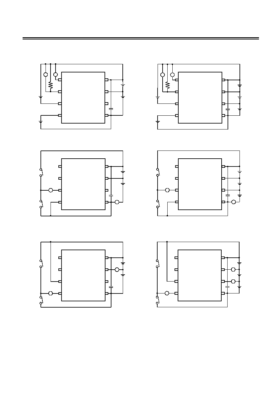
Test Circuits
1. Overcharge detection voltage, overcharge release voltage, overdischarge detection
voltage, overdischarge release voltage
(Test condition 1, test circuit 1)
Confirm that V1
= V2 = 3.5 V (S-8253A Series), V1 = V2 = V3 = 3.5 V (S-8253B Series), V4 = 0 V, V5 = 0 V,
and the COP and DOP pins are low (V
DD
◊ 0.1 V or lower) (this status is referred to as the initial status).
∑
∑
∑
∑ Overcharge detection voltage 1 (V
CU1
), overcharge release voltage 1 (V
CL1
)
Overcharge detection voltage 1 (V
CU1
) is the voltage of V1 when the voltage of the COP pin is high (V
DD
◊
0.9 V or more) after the V1 voltage has been gradually increased starting at the initial status. Overcharge
release voltage 1 (V
CL1
) is the voltage of V1 when the voltage at the COP pin is low after the V1 voltage has
been gradually decreased.
∑
∑
∑
∑ Overdischarge detection voltage 1 (V
DL1
), overdischarge release voltage 1 (V
DU1
)
Overdischarge detection voltage 1 (V
DL1
) is the voltage of V1 when the voltage of the DOP pin is high after
the V1 voltage has been gradually decreased starting at the initial status. Overdischarge release voltage
1 (V
DU1
) is the voltage of V1 when the voltage at the DOP pin is low after the V1 voltage has been gradually
increased.
By changing Vn (n
= 2: S-8253A Series, n = 2, 3: S-8253B Series) the overcharge detection voltage (V
CUn
),
overcharge release voltage (V
CLn
), overdischarge detection voltage (V
DLn
), and overdischarge release
voltage (V
DUn
) can be measured in the same way as when n
= 1.
2. Overcurrent detection voltage
(Test condition 2, test circuit 1)
Confirm that V1
= V2 = 3.5 V (S-8253A Series), V1 = V2 = V3 = 3.5 V (S-8253B Series), V4 = 0 V, V5 = 0 V,
and the COP and DOP pins are low (this status is referred to as the initial status).
∑
∑
∑
∑ Overcurrent detection voltage 1 (V
IOV1
)
Overcurrent detection voltage 1 (V
IOV1
) is the voltage of V5 when the voltages of the COP and DOP pins
are high after the V5 voltage has been gradually increased starting at the initial status.
∑
∑
∑
∑ Overcurrent detection voltage 2 (V
IOV2
)
Overcurrent detection voltage 2 (V
IOV2
) is the voltage of V5 when the voltages of the COP and DOP pins
are high within the minimum and maximum values of overcurrent detection time 2 (t
IOV2
) after the voltage
of V5 was instantaneously increased (within 10
µs) starting at the initial status.
∑
∑
∑
∑ Overcurrent detection voltage 3 (V
IOV3
)
Overcurrent detection voltage 3 (V
IOV3
) is the voltage of V5 when the voltages of the COP and DOP pins
are high within the minimum and maximum values of overcurrent detection time 3 (t
IOV3
) after the voltage
of V5 was instantaneously increased (within 10
µs) starting at the initial status.

BATTERY PROTECTION IC FOR 2-SERIAL OR 3-SERIAL-CELL PACK
Rev.2.1
_00
S-8253A/B Series
Seiko Instruments Inc.
9
3. Overcharge detection delay time, overdischarge detection delay time
(Test condition 3, test circuit 1)
Confirm that V1
= V2 = 3.5 V (S-8253A Series), V1 = V2 = V3 = 3.5 V (S-8253B Series), V4 = 0 V, V5 = 0 V,
and the COP and DOP pins are low (this status is referred to as the initial status).
∑
∑
∑
∑ Overcharge detection delay time (t
CU
)
The overcharge detection delay time (t
CU
) is the time it takes for the voltage of the COP pin to change from
low to high after the voltage of V1 is instantaneously changed from overcharge detection voltage 1 (V
CU1
)
- 0.2 V to overcharge detection voltage 1 (V
CU1
)
+ 0.2 V (within 10 µs) starting at the initial status.
∑
∑
∑
∑ Overdischarge detection delay time (t
DL
)
The overdischarge detection delay time (t
DL
) is the time it takes for the voltage of the DOP pin to change
from low to high after the voltage of V1 is instantaneously changed from overdischarge detection voltage 1
(V
DL1
)
+ 0.2 V to overdischarge detection voltage 1 (V
DL1
)
- 0.2 V (within 10 µs) starting at the initial status.
4. Overcurrent detection delay time
(Test condition 4, test circuit 1)
Confirm that V1
= V2 = 3.5 V (S-8253A Series), V1 = V2 = V3 = 3.5 V (S-8253B Series), V4 = 0 V, V5 = 0 V,
and the COP and DOP pins are low (this status is referred to as the initial status).
∑
∑
∑
∑ Overcurrent detection delay time 1 (t
IOV1
)
Overcurrent detection delay time 1 (t
IOV1
) is the time it takes for the voltage of the DOP pin to change from
low to high after the voltage of V5 is instantaneously changed to 0.35 V (within 10
µs) starting at the initial
status.
∑
∑
∑
∑ Overcurrent detection delay time 2 (t
IOV2
)
Overcurrent detection delay time 2 (t
IOV2
) is the time it takes for the voltage of the DOP pin to change from
low to high after the voltage of V5 is instantaneously changed to 0.7 V (within 10
µs) starting at the initial
status.
∑
∑
∑
∑ Overcurrent detection delay time 3 (t
IOV3
)
Overcurrent detection delay time 3 (t
IOV3
) is the time it takes for the voltage of the DOP pin to change from
low to high after the voltage of V5 is instantaneously changed to 1.6 V (within 10
µs) starting at the initial
status.
5. Power consumption during operation, power consumption at power-down
(Test condition 5, test circuit 2)
∑
∑
∑
∑ Power consumption during operation (I
OPE
), power consumption at power-down (I
PDN
)
The power consumption during operation (I
OPE
) is the current of the VSS pin (I
SS
) when V1
= V2 = 3.5 V
(S-8253A Series), V1
= V2 = V3 = 3.5 V (S-8253B Series), S1 = ON, and S2 = OFF.
The power consumption at power-down (I
PDN
) is the current of the VSS pin (I
SS
) when V1
= V2 = 1.5 V
(S-8253A Series), V1
= V2 = V3 = 1.5 V (S-8253B Series), S1 = OFF, and S2 = ON.

BATTERY PROTECTION IC FOR 2-SERIAL OR 3-SERIAL-CELL PACK
S-8253A/B Series
Rev.2.1
_00
Seiko Instruments Inc.
10
6. Resistance between VMP and VDD, resistance between VMP and VSS
(Test condition 6, test circuit 2)
Confirm that V1
= V2 = 3.5 V (S-8253A Series), V1 = V2 = V3 = 3.5 V (S-8253B Series), S1 = ON, and S2 =
OFF (this status is referred to as the initial status).
∑
∑
∑
∑ Resistance between VMP and VDD (R
VMD
)
The resistance between VMP and VDD (R
VMD
) is determined based on the current of the VMP pin (I
VMD
)
after S1 and S2 are switched to OFF and ON, respectively, starting at the initial status.
S-8253A Series: R
VMD
= (V1 + V2)/I
VMD
S-8253B Series: R
VMD
= (V1 + V2 + V3)/I
VMD
∑
∑
∑
∑ Resistance between VMP and VSS (R
VMS
)
The resistance between VMP and VSS (R
VMS
) is determined based on the current of the VMP pin (I
VMS
)
after V1
= V2 = 1.8 V (S-8253A Series) or V1 = V2 = V3 = 1.8 V (S-8253B Series) are set starting at the
initial status.
S-8253A Series: R
VMS
= (V1 + V2)/I
VMS
S-8253B Series: R
VMS
= (V1 + V2 + V3)/I
VMS
7. CTL pin input voltage
(Test condition 7, test circuit 1)
Confirm that V1
= V2 = 3.5 V (S-8253A Series), V1 = V2 = V3 = 3.5 V (S-8253B Series), V4 = 0 V, V5 = 0 V,
and the COP and DOP pins are low (this status is referred to as the initial status).
∑
∑
∑
∑ CTL pin input voltage (high) (V
CTLH
)
The CTL pin input voltage (high) (V
CTLH
) is the voltage of V4 when the voltages of the COP and DOP pins
are high after the voltage of V4 has been gradually increased starting at the initial status.
Confirm that V1
= V2 = 3.5 V (S-8253A Series), V1 = V2 = V3 = 3.5 V (S-8253B Series), V4 = 0 V, V5 = 0.35
V, and the COP and DOP pins are high (this status is referred to as the initial status).
∑
∑
∑
∑ CTL pin input voltage (low) (V
CTLL
)
The CTL pin input voltage (low) (V
CTLL
) is the voltage of V4 when the voltages of the COP and DOP pins
are low after the voltage of V4 has been gradually decreased starting at the initial status.
8. CTL pin current
(Test condition 8, test circuit 3)
∑
∑
∑
∑ CTL current (high) (I
CTLH
), CTL pin current (low) (I
CTLL
)
The CTL pin current (high) (I
CTLH
) is the current that flows through the CTL pin when V1
= V2 = 3.5 V
(S-8253A Series), V1
= V2 = V3 = 3.5 V (S-8253B Series), and S3 = ON, S4 = OFF. The CTL current (low)
(I
CTLL
) is the current that flows through the CTL pin when S3
= OFF and S4 = ON after that.

BATTERY PROTECTION IC FOR 2-SERIAL OR 3-SERIAL-CELL PACK
Rev.2.1
_00
S-8253A/B Series
Seiko Instruments Inc.
11
9. VC1 pin current, VC2 pin current
(Test condition 9, test circuit 3)
∑
∑
∑
∑ VC1 pin current (I
VC1
), VC2 pin current (I
VC2
)
The VC1 pin current (I
VC1
) is the current that flows through the VC1 pin when V1
= V2 = 3.5 V (S-8253A
Series), V1
= V2 = V3 = 3.5 V (S-8253B Series), and S3 = OFF, S4 = ON. Similarly, the VC2 pin current
(I
VC2
) is the current that flows through the VC2 pin under these conditions (S-8253B Series only).
10. COP pin leakage current, COP pin sink current
(Test condition 10, test circuit 4)
∑
∑
∑
∑ COP pin leakage current (I
COH
), COP pin sink current (I
COL
)
The COP pin leakage current (I
COH
) is the current that flows through the COP pin when V1
= V2 = 12 V
(S-8253A Series), V1
= V2 = V3 = 8 V (S-8253B Series), S6 = S7 = S8 = OFF, and S5 = ON.
The COP pin sink current (I
COL
) is the current that flows through the COP pin when V1
= V2 = 3.5 V
(S-8253A Series), V1
= V2 = V3 = 3.5 V (S-8253B Series), V6 = 0.5 V, S5 = S7 = S8 = OFF, and S6 = ON.
11. DOP pin source current, DOP pin sink current
(Test condition 11, test circuit 4)
∑
∑
∑
∑ DOP pin source current (I
DOH
), DOP pin sink current (I
DOL
)
The DOP pin source current (I
DOH
) is the current that flows through the DOP pin when V1
= V2 = 1.8 V
(S-8253A Series), V1
= V2 = V3 = 1.8 V (S-8253B Series), V7 = 0.5 V, S5 = S6 = S8 = OFF, and S7 = ON.
The DOP pin sink current (I
DOL
) is the current that flows through the DOP pin when V1
= V2 = 3.5 V
(S-8253A Series), V1
= V2 = V3 = 3.5 V (S-8253B Series), V8 = 0.5 V, S5 = S6 = S7 = OFF, and S8 = ON.
12. 0 V charge start battery charger voltage or 0 V charge inhibition battery voltage
(Test condition 12, test circuit 5)
∑
∑
∑
∑ 0 V charge start battery charger voltage (V
0CHA
): Products that available 0 V charge
The COP pin voltage should be lower than V
0CHA
max.
-1 V when V1 = V2 = 0 V (S-8253A Series), V1 = V2
= V3 = 0 V (S-8253B Series), and V9 = V
VMP
= V
0CHA
max..
∑
∑
∑
∑ 0 V charge inhibition battery voltage (V
0INH
): Products that unavailable 0 V charge
The COP pin voltage should be higher than V
VMP
- 1 V when V1 = V2 = V
0INH
min. (S-8253A Series), V1
=
V2
= V3 = V
0INH
min. (S-8253B Series), and V9
= V
VMP
= 24 V.
BATTERY PROTECTION IC FOR 2-SERIAL OR 3-SERIAL-CELL PACK
S-8253A/B Series
Rev.2.1
_00
Seiko Instruments Inc.
12
V5
1 M
DOP
1
COP
2
VMP
3
CTL
4
8
VDD
7
VC1
6
VC2
5
VSS
V
V
1
µF
V2
V4
V1
S-8253A
V5
1 M
V
V
1
µF
V2
V4
V1
DOP
1
COP
2
VMP
3
CTL
4
8
VDD
7
VC1
6
VC2
5
VSS
S-8253B
V3
Test Circuit 1
S1
DOP
1
COP
2
VMP
3
CTL
4
8
VDD
7
VC1
6
VC2
5
VSS
A
1
µF
V2
S2
V1
S-8253A
A
S1
DOP
1
COP
2
VMP
3
CTL
4
8
VDD
7
VC1
6
VC2
5
VSS
A
1
µF
V2
S2
V1
S-8253B
A
V3
Test Circuit 2
S3
DOP
1
COP
2
VMP
3
CTL
4
8
VDD
7
VC1
6
VC2
5
VSS
A
1
µF
V2
S4
V1
S-8253A
A
S3
DOP
1
COP
2
VMP
3
CTL
4
8
VDD
7
VC1
6
VC2
5
VSS
A
1
µF
V2
S4
V1
S-8253B
A
A
V3
Test Circuit 3
Figure 4 Test Circuit (1/2)

BATTERY PROTECTION IC FOR 2-SERIAL OR 3-SERIAL-CELL PACK
Rev.2.1
_00
S-8253A/B Series
Seiko Instruments Inc.
13
S5
DOP
1
COP
2
VMP
3
CTL
4
8
VDD
7
VC1
6
VC2
5
VSS
A
1
µF
V2
S6
V1
S-8253A
A
V8
S7
S8
V6
V7
S5
DOP
1
COP
2
VMP
3
CTL
4
8
VDD
7
VC1
6
VC2
5
VSS
A
1
µF
V2
S6
V1
S-8253B
A
V8
S7
S8
V6
V7
V3
Test Circuit 4
1 M
DOP
1
COP
2
VMP
3
CTL
4
8
VDD
7
VC1
6
VC2
5
VSS
V
1
µF
V2
V9
V1
S-8253A
1 M
DOP
1
COP
2
VMP
3
CTL
4
8
VDD
7
VC1
6
VC2
5
VSS
V
1
µF
V2
V9
V1
S-8253B
V3
Test Circuit 5
Figure 4 Test Circuit (2/2)

BATTERY PROTECTION IC FOR 2-SERIAL OR 3-SERIAL-CELL PACK
S-8253A/B Series
Rev.2.1
_00
Seiko Instruments Inc.
14
Description of Operation
Remark Refer to " Standard Circuit ".
1.
Normal status
When all of the battery voltages are in the range from V
DLn
to V
CUn
and the discharge current is lower than
the specified value (the VMP pin voltage is higher than V
DD
-
V
IOV1
), the charging and discharging FETs are
turned on.
Caution When the battery is connected for the first time, discharging may not be enabled. In this
case, short the VMP and VDD pins or connect the charger to restore the normal status.
2.
Overcharge status
When any one of the battery voltages becomes higher than V
CUn
and the state continues for t
CU
or longer,
the COP pin becomes high impedance. Because the COP pin is pulled up to the EB
+
pin voltage by an
external resistor, the charging FET is turned off to stop charging. This is called the overcharge status. The
overcharge status is released when one of the following two conditions holds.
a) All battery voltages become V
CLn
or lower.
b) All of the battery voltages are V
CUn
or lower, and the VMP pin voltage is V
DD
- V
IOV1
or lower (Since the
discharge current flows through the body diode of the charging FET immediately after discharging is
started when the charger is removed and a load is connected, the VMP pin voltage momentarily
decreases by approximately 0.6 V from the VDD pin voltage. The IC detects this voltage and
releases the overcharging status.)
3.
Overdischarge status
When any one of the battery voltages becomes lower than V
DLn
and the state continues for t
DL
or longer, the
DOP pin voltage becomes V
DD
level, and the discharging FET is turned off to stop discharging. This is
called the overdischarging status. After discharging is stopped due to the overdischarge status, the
S-8253A/B Series enters the power-down status.
4.
Power-down status
When discharging has stopped due to the overdischarge status, the VMP pin is pulled down to the V
SS
level
by the RVSM resistor. When the VMP pin voltage is lower than V
DD
/2, the S-8253A/B Series enters the
power-down status. In the power-down status, almost all the circuits of the S-8253A/B Series stop and the
current consumption is I
PDN
or lower. The conditions of each output pin are as follows.
a) COP
Hi-Z
b) DOP
V
DD
The power-down status is released when the following condition holds.
a) The VMP pin voltage is V
DD
/2 or higher. (A charger is connected.
)
The overdischarging status is released when the following condition holds.
a) All of the battery voltages are V
DLn
or higher, and the VDD pin voltage is V
DD
/2 or higher. (A charger
is connected.)

BATTERY PROTECTION IC FOR 2-SERIAL OR 3-SERIAL-CELL PACK
Rev.2.1
_00
S-8253A/B Series
Seiko Instruments Inc.
15
5.
Overcurrent status
The S-8253A/B Series has three overcurrent detection levels (V
IOV1
, V
IOV2
, and V
IOV3
) and three overcurrent
detection delay times (t
IOV1
, t
IOV2
, and t
IOV3
) corresponding to each overcurrent detection level. When the
discharging current becomes higher than the specified value (the difference of the voltages of the VMP and
VDD pins is greater than V
IOV1
) and the state continues for t
IOV1
or longer, the S-8253A/B Series enters the
overcurrent status, in which the DOP pin voltage becomes V
DD
level to turn off the discharging FET to stop
discharging, the COP pin becomes high impedance and is pulled up to the EB
+ pin voltage to turn off the
charging FET to stop charging, and the VMP pin is pulled up to the V
DD
voltage by the internal resistor
RVMD. Operation of overcurrent detection levels 2, 3 (V
IOV2
, V
IOV3
) and overcurrent detection delay times 2,
3 (t
IOV2
, t
IOV3
) are the same as for V
IOV1
and t
IOV1
.
The overcurrent status is released when the following condition holds.
a) The VMP pin voltage is V
DD
- V
IOV1
or higher because a charger is connected or the load is released.
Caution The impedance that enables automatic restoration varies depending on the battery
voltage and set value of overcurrent detection voltage 1.
6. 0 V battery charge function
Regarding the charging of a self-discharged battery (0 V battery), the S-8253A/B Series has two functions
from which one should be selected.
a) 0 V battery charging is allowed (0 V battery charging is available)
When the charger voltage is higher than V
0CHA
, the 0 V battery can be charged.
b) 0 V battery charging is prohibited (0 V battery charging is unavailable)
When one of the battery voltages is lower than V
0INH
, the 0 V battery cannot be charged.
Caution When the VDD pin voltage is lower than the minimum value of V
DSOP
, the operation of the
S-8253A/B Series is not guaranteed.
BATTERY PROTECTION IC FOR 2-SERIAL OR 3-SERIAL-CELL PACK
S-8253A/B Series
Rev.2.1
_00
Seiko Instruments Inc.
16
7.
Delay circuit
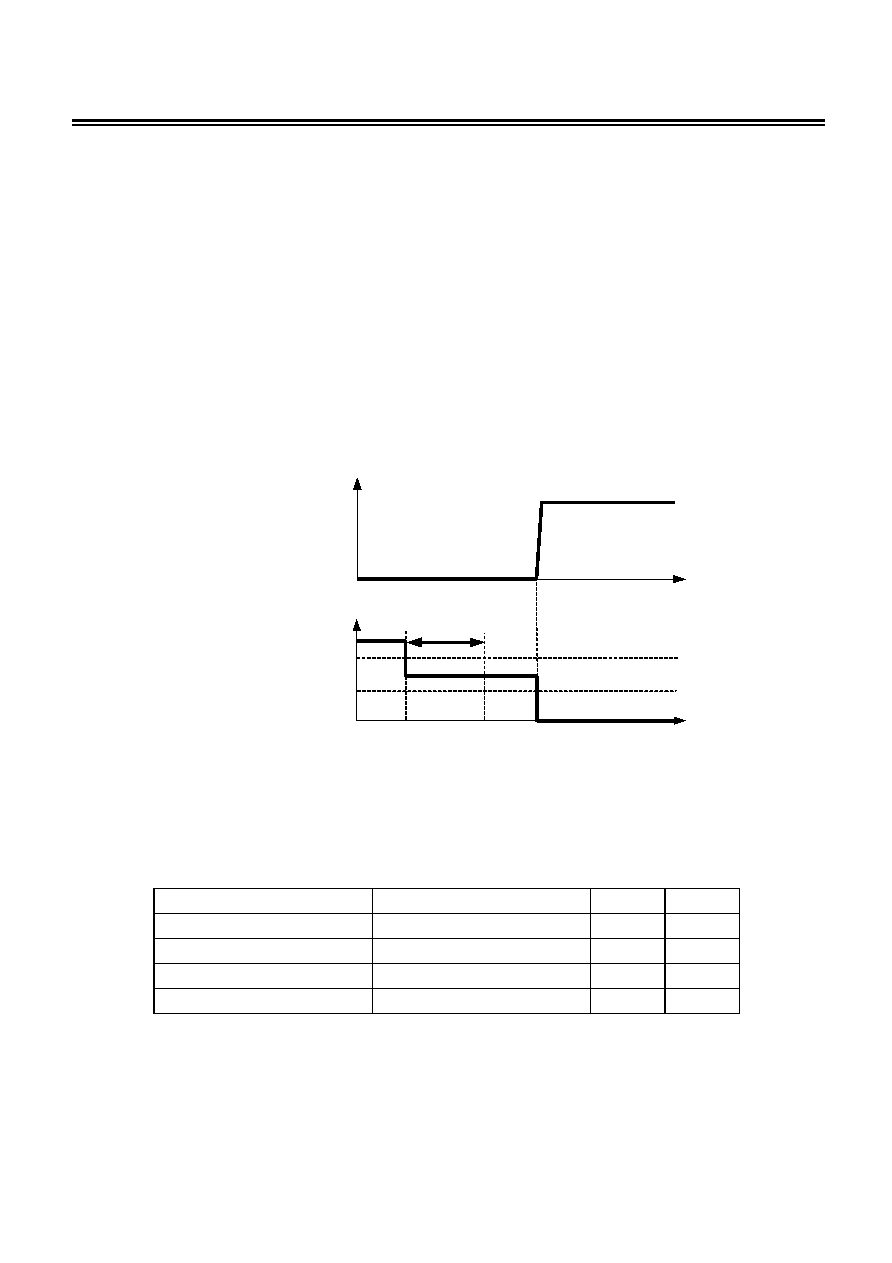
The following detection delay times are determined by dividing a clock of approximately 3.57 kHz by the
counter.
(Example)
Oscillator clock cycle (T
CLK
): 280
µs
Overcharge detection delay time (t
CU
): 1.15
s
Overdischarge detection delay time (t
DL
): 144
ms
Overcurrent detection delay time 1 (t
IOV1
): 9
ms
Overcurrent detection delay time 2 (t
IOV2
): 4.5
ms
Caution The overcurrent detection delay time 2(t
IOV2
) and overcurrent detection delay time 3(t
IOV3
)
start when the overcurrent detection voltage 1(V
IOV1
) is detected. As soon as the
overcurrent detection voltage 2(V
IOV2
) or overcurrent detection voltage 3(V
IOV3
)is detected
over the detection delay time for overcurrent 2(t
IOV2
) or overcurrent 3(t
IOV3
) after the
detection of overcurrent 1, the S-8253A/B turns the discharging control FET off.
V
DD
DOP pin voltage
V
SS
Overcurrent detection
delay time 2 (t
IOV2
)
V
IOV1
Time
V
DD
VMP pin voltage
V
SS
Time
V
IOV2
8. CTL pin
The S-8253A/B Series has a control pin for charge/discharge control and reducing test time. The levels, "L",
"H", and "M", of the voltage input to the CTL pin determine the status of the S-8253A/B Series: normal
operation, charge/discharge inhibition, or test time reduction. The CTL pin takes precedence over the
battery protection circuit. During normal use, short the CTL and VSS pins.
Table 7 Conditions Set by CTL Pin
CTL Pin Potential
Status of IC
COP Pin
DOP Pin
Open Charge/discharge
inhibited
status
Hi-Z
V
DD
High (V
CTL
V
CTLH
) Charge/discharge
inhibited
status
Hi-Z
V
DD
Middle (V
CTLL
< V
CTL
< V
CTLH
)
Delay time reduced status
*1
(*2) (*2)
Low (V
CTLL
V
CTL
) Normal
status
(*2) (*2)
*1. In the delay time reduced status, delay times are reduced in 1/60 to 1/30 scale.
*2. The pin status is controlled by the voltage detection circuit.
Caution1. If the potential of the CTL pin is middle, overcurrent detection voltage 1 (V
IOV1
)
does not operate.
2. If you use the middle potential of the CTL pin, contact our sales office.
BATTERY PROTECTION IC FOR 2-SERIAL OR 3-SERIAL-CELL PACK
Rev.2.1
_00
S-8253A/B Series
Seiko Instruments Inc.
17
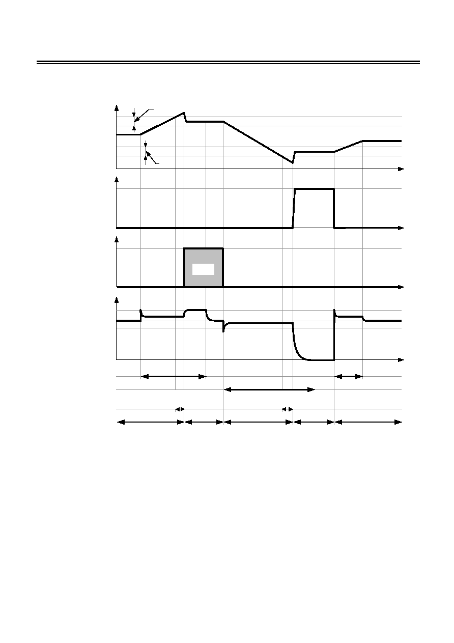
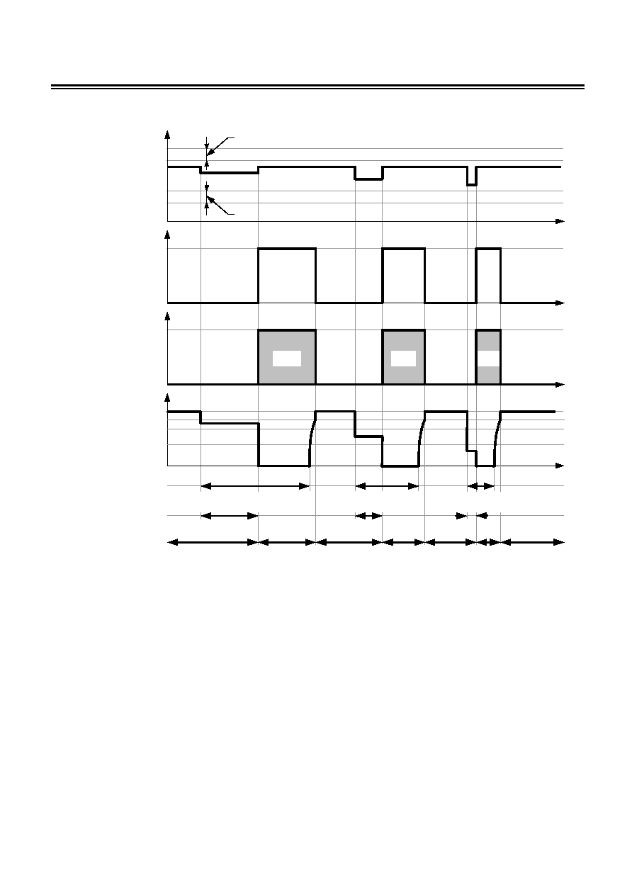
Operation Timing Chart
1. Overcharge and overdischarge detection
(n
= 1 to 3)
V
CUn
V
DUn
V
DLn
V
CLn
Battery
voltage
Hi-Z
V
SS
COP
pin voltage
V
DD
DOP
pin voltage
V
SS
Charger
connection
Load
connection
Mode
*1
Overcharge detection
delay time (t
CU
)
Overdischarge detection
delay time (t
DL
)
<1> <2> <1> <3> <1>
V
IOV1
V
SS
VMP
pin voltage
V
DD
V
EB
+
V
EB
+
V
HC
V
HD
*1. <1>: Normal mode
<2>: Overcharge mode
<3>: Overdischarge mode
Remark The charger is assumed to charge with a constant current. V
EB
+
indicates the open voltage of
the charger.
Figure 5
BATTERY PROTECTION IC FOR 2-SERIAL OR 3-SERIAL-CELL PACK
S-8253A/B Series
Rev.2.1
_00
Seiko Instruments Inc.
18
2. Overcurrent detection
V
CUn
V
DUn
V
DLn
(n
= 1 to 3)
V
CLn
Battery
voltage
V
HC
V
HD
V
DD
DOP
pin voltage
V
SS
Hi-Z
V
EB
+
V
SS
COP
pin voltage
Hi-Z
Hi-Z
V
DD
V
V
SS
VMP
pin voltage V
IOV3
V
Load
connection
Mode
*1
Overcurrent detection
delay time 1 (t
IOV1
)
<1> <2>
<1>
<1>
Overcurrent detection
delay time 2 (t
IOV2
)
Overcurrent detection
delay time 3 (t
IOV3
)
<2> <1>
<2>
V
IOV2
V
V
IOV1
V
*1. <1>: Normal mode
<2>: Overcurrent mode
Remark The charger is assumed to charge with a constant current. V
EB
+
indicates the open voltage of
the charger.
Figure 6

BATTERY PROTECTION IC FOR 2-SERIAL OR 3-SERIAL-CELL PACK
Rev.2.1
_00
S-8253A/B Series
Seiko Instruments Inc.
19
Standard Circuit
(1) S-8253A Series
EB
+
R
COP
R
VMP
R
DOP
R
CTL
EB
-
1 DOP
2 COP
3 VMP
4 CTL
8
VDD
7
VC1
6
VC2
5
VSS
S-8253A
R
VC1
C
VSS
C
VC1
R
VSS
Charging
FET
Discharging
FET
CTL
Figure 7
(2) S-8253B Series
EB
+
R
COP
R
VMP
R
DOP
R
CTL
EB
-
1 DOP
2 COP
3 VMP
4 CTL
8
VDD
7
VC1
6
VC2
5
VSS
S-8253B
R
VC1
C
VC2
C
VSS
C
VC1
R
VC2
R
VSS
Charging
FET
Discharging
FET
CTL
Figure 8

BATTERY PROTECTION IC FOR 2-SERIAL OR 3-SERIAL-CELL PACK
S-8253A/B Series
Rev.2.1
_00
Seiko Instruments Inc.
20
Table 8 Recommended Value for External Parts
Caution The standard circuit above does not guarantee proper operation.
Evaluation in the actual application is needed to determine the
correct
constants.
Precautions
∑
The application conditions for the input voltage, output voltage, and load current should not exceed the
package power dissipation.
∑
Batteries can be connected in any order, however, there may be cases when discharging cannot be
performed when a battery is connected. In this case, short the VMP and VDD pins or connect the battery
charger to return to the normal mode.
∑
Do not apply an electrostatic discharge to this IC that exceeds the performance ratings of the built-in
electrostatic protection circuit.
∑
SII claims no responsibility for any disputes arising out of or in connection with any infringement by
products including this IC of patents owned by a third party.
No. Symbol
Recommended
Value
Range Unit
1 R
VC1
1
0 to 1
k
2 R
VC2
1
0 to 1
k
3 R
DOP
5.1
2 to 10
k
4 R
COP
1
0.1 to 1
M
5 R
VMP
5.1
1 to 10
k
6 R
CTL
0
0 to 100
k
7 R
VSS
0
0 to 51
8 C
VC1
0.1
0 to 0.33
µF
9 C
VC2
0.1
0 to 0.33
µF
10 C
VSS
1
0 to 10
µF

BATTERY PROTECTION IC FOR 2-SERIAL OR 3-SERIAL-CELL PACK
Rev.2.1
_00
S-8253A/B Series
Seiko Instruments Inc.
21
Characteristics (Typical Data)
(1) Current consumption
(a) S-8253AAA
1. I
OPE
≠ V
DD
2.
I
OPE
≠ Ta
I
OPE
[
µ
A]
0
5
10
15
20
40
35
30
25
20
15
10
5
0
I
OPE
[
µ
A]
-40
-25
0
25
50
75
85
40
35
30
25
20
15
10
5
0
V
DD
[V]
Ta [
∞C]
3. I
PDN
≠ V
DD
4.
I
PDN
≠ Ta
I
PD
N
[
µ
A]
0
5
10
15
20
0.10
0.09
0.08
0.07
0.06
0.05
0.04
0.03
0.02
0.01
0
I
PD
N
[
µ
A]
-40
-25
0
25
50
75
85
0.10
0.09
0.08
0.07
0.06
0.05
0.04
0.03
0.02
0.01
0
V
DD
[V]
Ta [
∞C]
(b) S-8253BAA
1. I
OPE
≠ V
DD
2.
I
OPE
≠ Ta
I
OPE
[
µ
A]
0
5
10
15
20
40
35
30
25
20
15
10
5
0
I
OPE
[
µ
A]
-40
-25
0
25
50
75
85
40
35
30
25
20
15
10
5
0
V
DD
[V]
Ta [
∞C]
3. I
PDN
≠ V
DD
4.
I
PDN
≠ Ta
I
PD
N
[
µ
A]
0
5
10
15
20
0.10
0.09
0.08
0.07
0.06
0.05
0.04
0.03
0.02
0.01
0
I
PD
N
[
µ
A]
-40
-25
0
25
50
75
85
0.10
0.09
0.08
0.07
0.06
0.05
0.04
0.03
0.02
0.01
0
V
DD
[V]
Ta [
∞C]

BATTERY PROTECTION IC FOR 2-SERIAL OR 3-SERIAL-CELL PACK
S-8253A/B Series
Rev.2.1
_00
Seiko Instruments Inc.
22
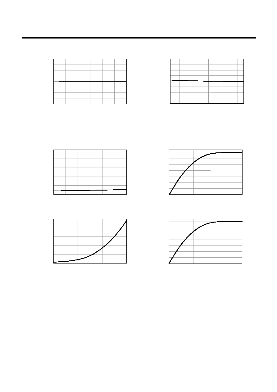
(2) Overcharge detection/release voltage, overdischarge detection/release voltage, overcurrent detection
voltage, and delay times
S-8253AAA, S-8253BAA
1. V
CU
≠ Ta
2. V
CL
≠ Ta
V
CU
[V]
4.375
4.370
4.365
4.360
4.355
4.350
4.345
4.340
4.335
4.330
4.325
-40
-25
0
25
50
75
85
V
CL
[V]
-40
-25
0
25
50
75
85
4.10
4.09
4.08
4.07
4.06
4.05
4.04
4.03
4.02
4.01
4.00
Ta [
∞C]
Ta [
∞C]
3. V
DU
≠ Ta
4. V
DL
≠ Ta
V
DU
[V]
-40
-25
0
25
50
75
85
2.80
2.78
2.76
2.74
2.72
2.70
2.68
2.66
2.64
2.62
2.60
V
DL
[V]
-40
-25
0
25
50
75
85
2.48
2.46
2.44
2.42
2.40
2.38
2.36
2.34
2.32
Ta [
∞C]
Ta [
∞C]
5. t
CU
≠ Ta
6. t
DL
≠ Ta
t
CU
[m
s]
-40
-25
0
25
50
75
85
1320
1220
1120
1020
920
1380
t
DL
[m
s]
-40
-25
0
25
50
75
85
165
155
145
135
125
115
173
Ta [
∞C]
Ta [
∞C]
7. V
IOV1
≠ V
DD
8.
V
IOV1
≠ Ta
V
IO
V
1
[V]
0.325
0.320
0.315
0.310
0.305
0.300
0.295
0.290
0.285
0.280
0.275
7
8
10
11
12
9
13
V
IO
V
1
[V]
-40
-25
0
25
50
75
85
0.325
0.320
0.315
0.310
0.305
0.300
0.295
0.290
0.285
0.280
0.275
V
DD
[V]
Ta [
∞C]
BATTERY PROTECTION IC FOR 2-SERIAL OR 3-SERIAL-CELL PACK
Rev.2.1
_00
S-8253A/B Series
Seiko Instruments Inc.
23
9. V
IOV2
≠ V
DD
10.
V
IOV2
≠ Ta
V
IO
V
2
[V]
0.60
0.58
0.56
0.54
0.52
0.50
0.48
0.46
0.44
0.42
0.40
7
8
10
11
12
9
13
V
IO
V
2
[V]
0.60
0.58
0.56
0.54
0.52
0.50
0.48
0.46
0.44
0.42
0.40
-40
-25
0
25
50
75
85
V
DD
[V]
Ta [
∞C]
11. V
IOV3
≠ V
DD
12.
V
IOV3
≠ Ta
V
IO
V
3
[V]
1.5
1.4
1.3
1.2
1.1
1.0
0.9
7
8
10
11
12
9
13
V
IO
V
3
[V]
-40
-25
0
25
50
75
85
1.5
1.4
1.3
1.2
1.1
1.0
0.9
V
DD
[V]
Ta [
∞C]
13. t
IOV1
≠ V
DD
14.
t
IOV1
≠ Ta
t
IO
V
1
[m
s]
10.8
10.4
10.0
9.6
9.2
8.8
8.4
8.0
7.6
7.2
7
8
10
11
12
9
13
t
IO
V
1
[m
s]
-40
-25
0
25
50
75
85
10.8
10.4
10.0
9.6
9.2
8.8
8.4
8.0
7.6
7.2
V
DD
[V]
Ta [
∞C]
15. t
IOV2
≠ V
DD
16.
t
IOV2
≠ Ta
t
IO
V
2
[m
s]
5.4
5.2
5.0
4.8
4.6
4.4
4.2
4.0
3.8
3.6
7
8
10
11
12
9
13
t
IO
V
2
[m
s]
-40
-25
0
25
50
75
85
5.4
5.2
5.0
4.8
4.6
4.4
4.2
4.0
3.8
3.6
V
DD
[V]
Ta [
∞C]
BATTERY PROTECTION IC FOR 2-SERIAL OR 3-SERIAL-CELL PACK
S-8253A/B Series
Rev.2.1
_00
Seiko Instruments Inc.
24
17. t
IOV3
≠ V
DD
18.
t
IOV3
≠ Ta
t
IO
V
3
[m
s]
0.38
0.36
0.34
0.32
0.30
0.28
0.26
0.24
0.22
7
8
10
11
12
9
13
t
IO
V
3
[m
s]
-40
-25
0
25
50
75
85
0.38
0.36
0.34
0.32
0.30
0.28
0.26
0.24
0.22
V
DD
[V]
Ta [
∞C]
(3) COP/DOP pin
S-8253AAA, S-8253BAA
1. I
COH
≠ V
COP
2.
I
COL
≠ V
COP
I
CO
H
[
µ
A]
0.10
0.08
0.06
0.04
0.02
0
0
4
12
16
20
8
24
I
CO
L
[m
A]
14
12
10
8
6
4
2
0
0
3.5
10.5
7.0
V
COP
[V]
V
COP
[V]
3. I
DOH
≠ V
DOP
4.
I
DOL
≠ V
DOP
I
DO
H
[m
A]
0
-0.5
-1.0
-1.5
-2.0
-2.5
0
1.8
5.4
3.6
I
DO
L
[m
A]
14
12
10
8
6
4
2
0
0
3.5
10.5
7.0
V
DOP
[V]
V
DOP
[V]
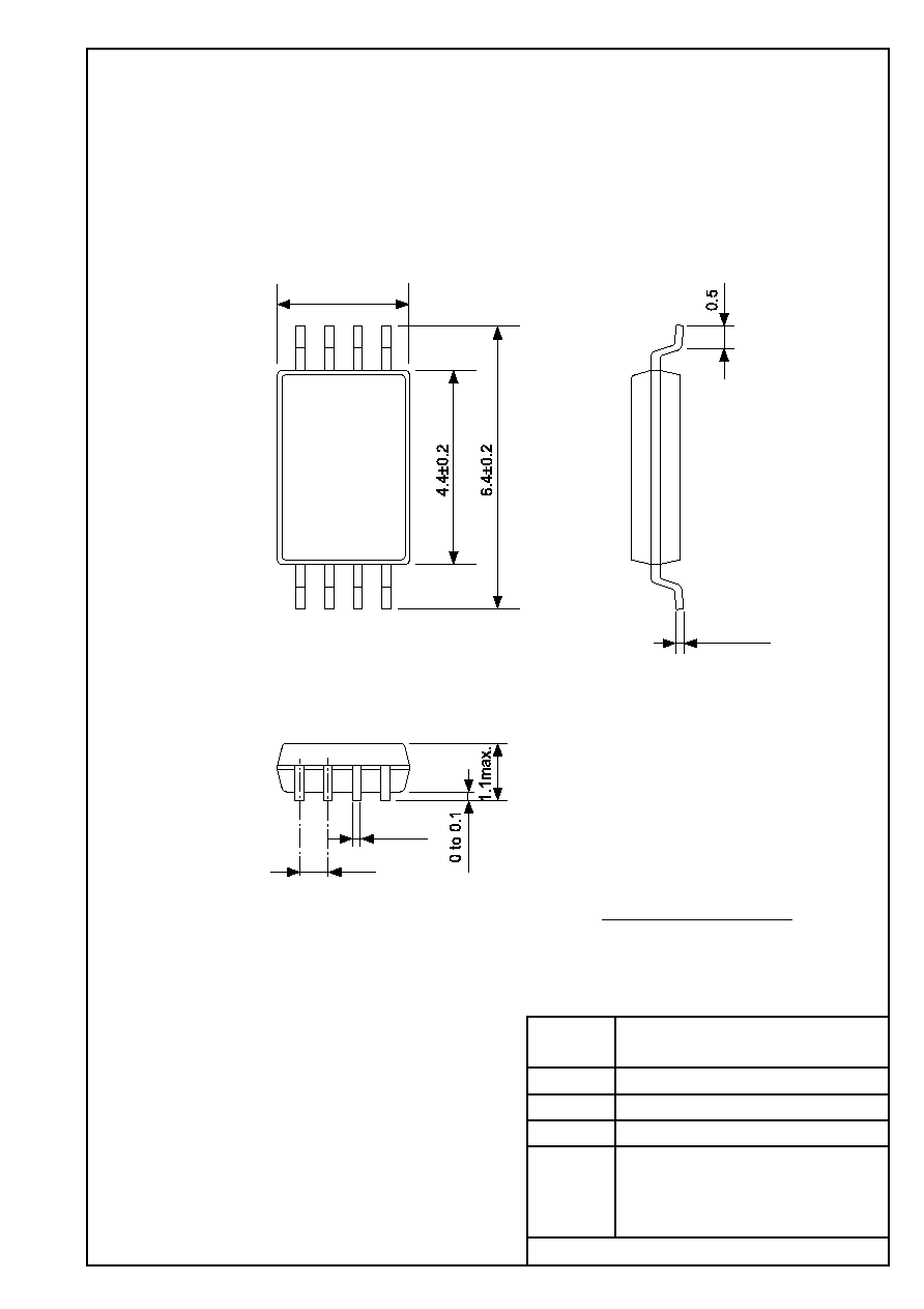
No.
TITLE
SCALE
UNIT
mm
Seiko Instruments Inc.
0.17±0.05
3.00
+0.3
-0.2
0.65
0.2±0.1
1
4
5
8
TSSOP8-A-PKG Dimensions
No. FT008-A-P-SD-1.1
FT008-A-P-SD-1.1

No.
TITLE
SCALE
UNIT
mm
Seiko Instruments Inc.
¯1.5
2.0±0.05
8.0±0.1
¯1.5
+0.1
-0
6.9±0.1
4.4±0.2
0.3±0.05
1
4
5
8
4.0±0.1
Feed direction
TSSOP8-D-Carrier Tape
No. FT008-D-C-SD-1.0
FT008-D-C-SD-1.0
+0.1
-0

No.
TITLE
SCALE
UNIT
mm
Seiko Instruments Inc.
QTY.
3,000
Enlarged drawing in the central part
TSSOP8-D-Reel
No. FT008-D-R-SD-1.0
FT008-D-R-SD-1.0
2±0.5
13.5±0.5
60∞
2±0.5
¯13±0.2
¯21±0.8

∑
The information described herein is subject to change without notice.
∑
Seiko Instruments Inc. is not responsible for any problems caused by circuits or diagrams described herein
whose related industrial properties, patents, or other rights belong to third parties. The application circuit
examples explain typical applications of the products, and do not guarantee the success of any specific
mass-production design.
∑
When the products described herein are regulated products subject to the Wassenaar Arrangement or other
agreements, they may not be exported without authorization from the appropriate governmental authority.
∑
Use of the information described herein for other purposes and/or reproduction or copying without the
express permission of Seiko Instruments Inc. is strictly prohibited.
∑
The products described herein cannot be used as part of any device or equipment affecting the human
body, such as exercise equipment, medical equipment, security systems, gas equipment, or any apparatus
installed in airplanes and other vehicles, without prior written permission of Seiko Instruments Inc.
∑
Although Seiko Instruments Inc. exerts the greatest possible effort to ensure high quality and reliability, the
failure or malfunction of semiconductor products may occur. The user of these products should therefore
give thorough consideration to safety design, including redundancy, fire-prevention measures, and
malfunction prevention, to prevent any accidents, fires, or community damage that may ensue.