
Rev.1.4
_10
BATTERY PROTECTION IC FOR SINGLE-CELL PACK
S-8261 Series
Seiko Instruments Inc.
1
The S-8261 series are lithium-ion/lithium polymer
rechargeable battery protection ICs incorporating high-
accuracy voltage detection circuit and delay circuit.
The S-8261 series are suitable for protection of single-
cell lithium ion/lithium polymer battery packs from
overcharge, overdischarge and overcurrent.
Features
(1) Internal high accuracy voltage detection circuit
∑ Overcharge detection voltage
3.9 V to 4.4 V (applicable in 5 mV step)
Accuracy:
±25 mV (+25∞C) and ±30 mV (-5∞C to +55∞C)
∑ Overcharge hysteresis voltage
0.0 V to 0.4 V
*1
Accuracy:
±25 mV
The overcharge hysteresis voltage can be selected from the range 0.0 V to 0.4 V in 50 mV step.
*1. Overcharge release voltage
= Overcharge detection voltage - Overcharge hysteresis voltage
(where overcharge release voltage
< 3.8 V is prohibited.)
∑ Overdischarge detection voltage
2.0 V to 3.0 V (10 mV step) Accuracy:
±50 mV
∑ Overdischarge hysteresis voltage 0.0 V to 0.7 V
*2
Accuracy:
±50 mV
The overdischarge hysteresis voltage can be selected from the range 0.0 V to 0.7 V in 100 mV step.
*2. Overdischarge release voltage
= Overdischarge detection voltage + Overdischarge hysteresis voltage
(where overdischarge release voltage
>3.4 V is prohibited.)
∑ Overcurrent 1 detection voltage
0.05 V to 0.3 V (10 mV step) Accuracy:
±15 mV
∑ Overcurrent 2 detection voltage
0. 5 V (fixed)
Accuracy:
±100 mV
(2) High voltage device is used for charger connection pins
(VM and CO pins: absolute maximum rating
= 28 V)
(3) Delay times (overcharge: t
CU
, overdischarge: t
DL
, overcurrent 1: t
lOV1
, overcurrent 2: t
lOV2
) are generated
by an internal circuit. No external capacitor is necessary.
Accuracy:
±20%
(4) Three-step overcurrent detection circuit is included.
(overcurrent 1, overcurrent 2 and load short-circuiting)
(5) Either charge function or charge inhibition function for 0 V battery can be selected.
(6) Charger detection function and abnormal charge current detection function
∑ The overdischarge hysteresis is released by detecting negative voltage at the VM pin (-0.7 V typ.).
(Charger detection function)
∑ When the output voltage of the DO pin is high and the voltage at the VM pin is equal to or lower than
the charger detection voltage (
-0.7 V typ.), the output voltage of the CO pin goes low.
(Abnormal charge current detection function)
(7) Low current consumption
∑ Operation
3.5
µA typ.
7.0
µA max.
∑ Power-down
0.1
µA max.
(8) Wide operating temperature range:
-40∞C to +85∞C
(9) Small package SOT-23-6, 6-Pin SNB(B)
Applications
Package
∑ Lithium-ion rechargeable battery packs
∑ SOT-23-6
(PKG drawing code: MP006-A)
∑ Lithium polymer rechargeable battery packs
∑ 6-Pin SNB(B) (PKG drawing code: BD006-A)
BATTERY PROTECTION IC for SINGLE-CELL PACK
S-8261 Series
Rev.1.4
_10
2
Seiko Instruments Inc.
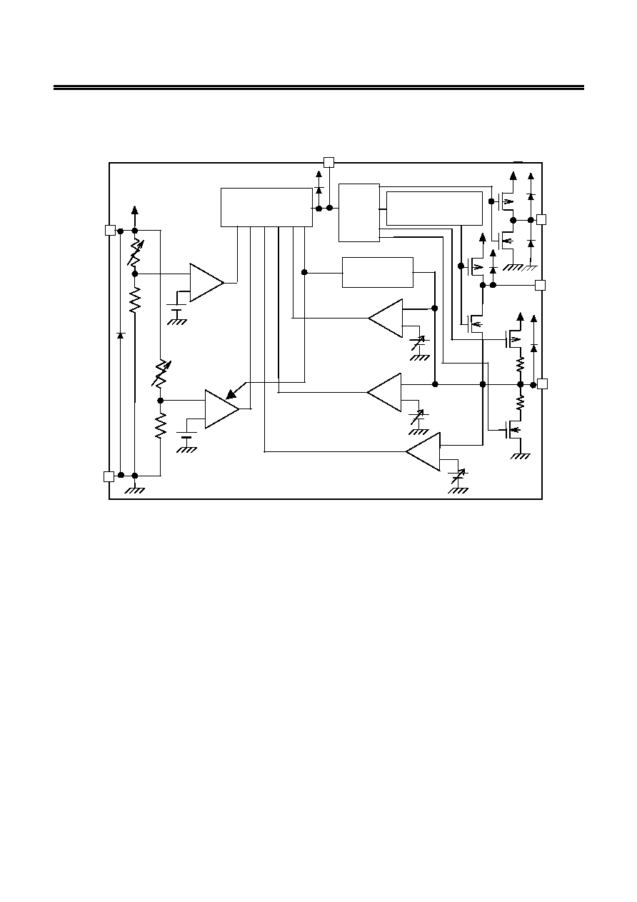
Block Diagram
+
-
-
+
VM
VSS
VDD
DP
CO
DO
Overcharge
detection
comparator
Overcurrent 2
detection comparator
-
+
-
+
Output control circuit
0 V battery
charge/charge inhibition
circuit
Overdischarge
detection
comparator
Load short-circuiting
detection comparator
Divider
control
logic
Oscillator control
circuit
R
VMD
R
VMS
Charger
detection circuit
Overcurrent 1
detection comparator
-
+
Remark Diodes in the figure are parasitic diodes.
Figure 1 Block Diagram
BATTERY PROTECTION IC for SINGLE-CELL PACK
Rev.1.4
_10
S-8261 Series
Seiko Instruments Inc.
3
Selection Guide
1. Product name selection guide
S
-8261A xx xx - xxx - xx
IC direction in tape specifications
*1
T2:
SOT-23-6
TF: 6-Pin SNB(B)
Product name (abbreviation)
*2
Package name (abbreviation)
MD:
SOT-23-6
BD: 6-Pin SNB(B)
Serial code
Assigned from AA to ZZ in alphabetical order
*1. Refer to the taping specifications at the end of this book.
*2. Refer to the product name list.
BATTERY PROTECTION IC for SINGLE-CELL PACK
S-8261 Series
Rev.1.4
_10
4
Seiko Instruments Inc.
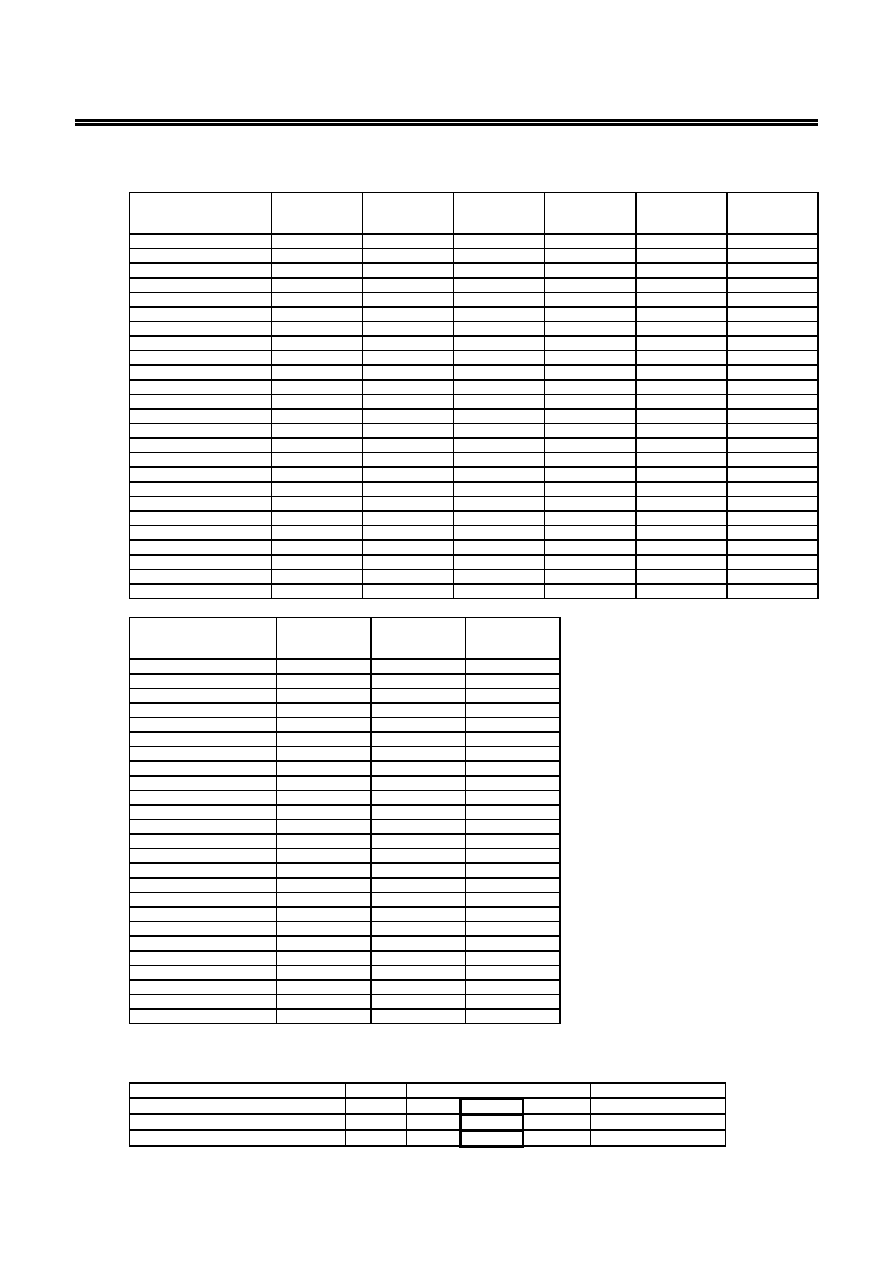
2. Product name list
Model No.
Overcharge
detection
voltage [V
CU
]
Overcharge
hysteresis
voltage [V
HC
]
Overdischarge
detection
voltage [V
DL
]
Overdischarge
hysteresis
voltage [V
HD
]
Overcurrent 1
detection
voltage [V
IOV1
]
0 V battery
charge
function
S-8261AAGMD-G2G-T2
4.28 V
0.2 V
2.3 V
0 V
0.16 V
Available
S-8261AAHMD-G2H-T2
4.28 V
0.2 V
2.3 V
0 V
0.08 V
Available
S-8261AAJBD-G2J-TF
4.325 V
0.25 V
2.5 V
0.4 V
0.15 V
Unavailable
S-8261AAJMD-G2J-T2
4.325 V
0.25 V
2.5 V
0.4 V
0.15 V
Unavailable
S-8261AALMD-G2L-T2
4.30 V
0.1 V
2.3 V
0 V
0.08 V
Unavailable
S-8261AAMMD-G2M-T2
4.30 V
0.1 V
2.3 V
0 V
0.2 V
Unavailable
S-8261AANMD-G2N-T2
4.275 V
0.1 V
2.3 V
0.1 V
0.1 V
Available
S-8261AAOMD-G2O-T2
4.28 V
0.2 V
2.3 V
0 V
0.13 V
Unavailable
S-8261AAPMD-G2P-T2
4.325 V
0.25 V
2.5 V
0.4 V
0.1 V
Unavailable
S-8261AARBD-G2R-TF
4.28 V
0.2 V
2.3 V
0 V
0.1 V
Available
S-8261AARMD-G2R-T2
4.28 V
0.2 V
2.3 V
0 V
0.1 V
Available
S-8261AASMD-G2S-T2
4.28 V
0.2 V
2.3 V
0 V
0.15 V
Unavailable
S-8261AAUMD-G2U-T2
4.275 V
0.1 V
2.3 V
0.1 V
0.1 V
Available
S-8261AAVBD-G2V-TF
4.3 V
0.2 V
2.3 V
0 V
0.13 V
Available
S-8261AAXMD-G2X-T2
4.35 V
0.1 V
2.3 V
0.1 V
0.1 V
Available
S-8261AAZMD-G2Z-T2
4.28 V
0.25 V
2.5 V
0.4 V
0.1 V
Unavailable
S-8261ABAMD-G3A-T2
4.35 V
0.2 V
2.5 V
0 V
0.2 V
Available
S-8261ABBMD-G3B-T2
4.275 V
0.2 V
2.3 V
0 V
0.13 V
Available
S-8261ABCMD-G3C-T2
4.30 V
0.2 V
2.3 V
0 V
0.13 V
Available
S-8261ABDBD-G3D-TF
4.28 V
0.2 V
2.3 V
0 V
0.13 V
Available
S-8261ABEBD-G3E-TF
4.275 V
0.2 V
2.3 V
0 V
0.1 V
Available
S-8261ABGBD-G3G-TF
4.275 V
0.2 V
2.3 V
0 V
0.1 V
Unavailable
S-8261ABHBD-G3H-TF
4.20 V
0 V
2.3 V
0 V
0.1 V
Available
S-8261ABIBD-G3I-TF
4.275 V
0.2 V
2.3 V
0 V
0.2 V
Unavailable
S-8261ABJMD-G3J-T2
4.28 V
0.2 V
3.0 V
0 V
0.08 V
Available
Model No.
Overcharge
detection delay
time
Overdischarge
detection delay
time
Overcurrent 1
detection delay
time
S-8261AAGMD-G2G-T2
1.2 s
144 ms
9 ms
S-8261AAHMD-G2H-T2
1.2 s
144 ms
9 ms
S-8261AAJBD-G2J-TF
1.2 s
144 ms
9 ms
S-8261AAJMD-G2J-T2
1.2 s
144 ms
9 ms
S-8261AALMD-G2L-T2
1.2 s
144 ms
9 ms
S-8261AAMMD-G2M-T2
1.2 s
144 ms
9 ms
S-8261AANMD-G2N-T2
1.2 s
144 ms
9 ms
S-8261AAOMD-G2O-T2
1.2 s
144 ms
9 ms
S-8261AAPMD-G2P-T2
1.2 s
144 ms
9 ms
S-8261AARBD-G2R-TF
1.2 s
144 ms
9 ms
S-8261AARMD-G2R-T2
1.2 s
144 ms
9 ms
S-8261AASMD-G2S-T2
1.2 s
144 ms
4.5 ms
S-8261AAUMD-G2U-T2
4.6 s
144 ms
9 ms
S-8261AAVBD-G2V-TF
4.6 s
144 ms
9 ms
S-8261AAXMD-G2X-T2
4.6 s
144 ms
9 ms
S-8261AAZMD-G2Z-T2
1.2 s
144 ms
9 ms
S-8261ABAMD-G3A-T2
4.6 s
144 ms
9 ms
S-8261ABBMD-G3B-T2
1.2 s
144 ms
9 ms
S-8261ABCMD-G3C-T2
1.2 s
144 ms
9 ms
S-8261ABDBD-G3D-TF
1.84 s
115 ms
7.2 ms
S-8261ABEBD-G3E-TF
1.2 s
144 ms
9 ms
S-8261ABGBD-G3G-TF
1.2
s 36
ms 9
ms
S-8261ABHBD-G3H-TF
0.3 s
36 ms
18 ms
S-8261ABIBD-G3I-TF 1.2
s 36
ms 9
ms
S-8261ABJMD-G3J-T2
1.2
s 36
ms 9
ms
It is possible to change the detection voltages of the product other than above.
The delay times can also be changed within the range listed bellow.
For details, please contact our sales office.
Delay time
Symbol
Selection range
Remarks
Overcharge detection delay time
t
CU
0.15 s
1.2 s
4.6 s
Choose from the left.
Overdischarge detection delay time
t
DL
36 ms
144 ms
290 ms
Choose from the left.
Overcurrent 1 detection delay time
t
lOV1
4.5 ms
9 ms
18 ms
Choose from the left.
Remark Values surrounded by bold lines are used in standard products.
BATTERY PROTECTION IC for SINGLE-CELL PACK
Rev.1.4
_10
S-8261 Series
Seiko Instruments Inc.
5
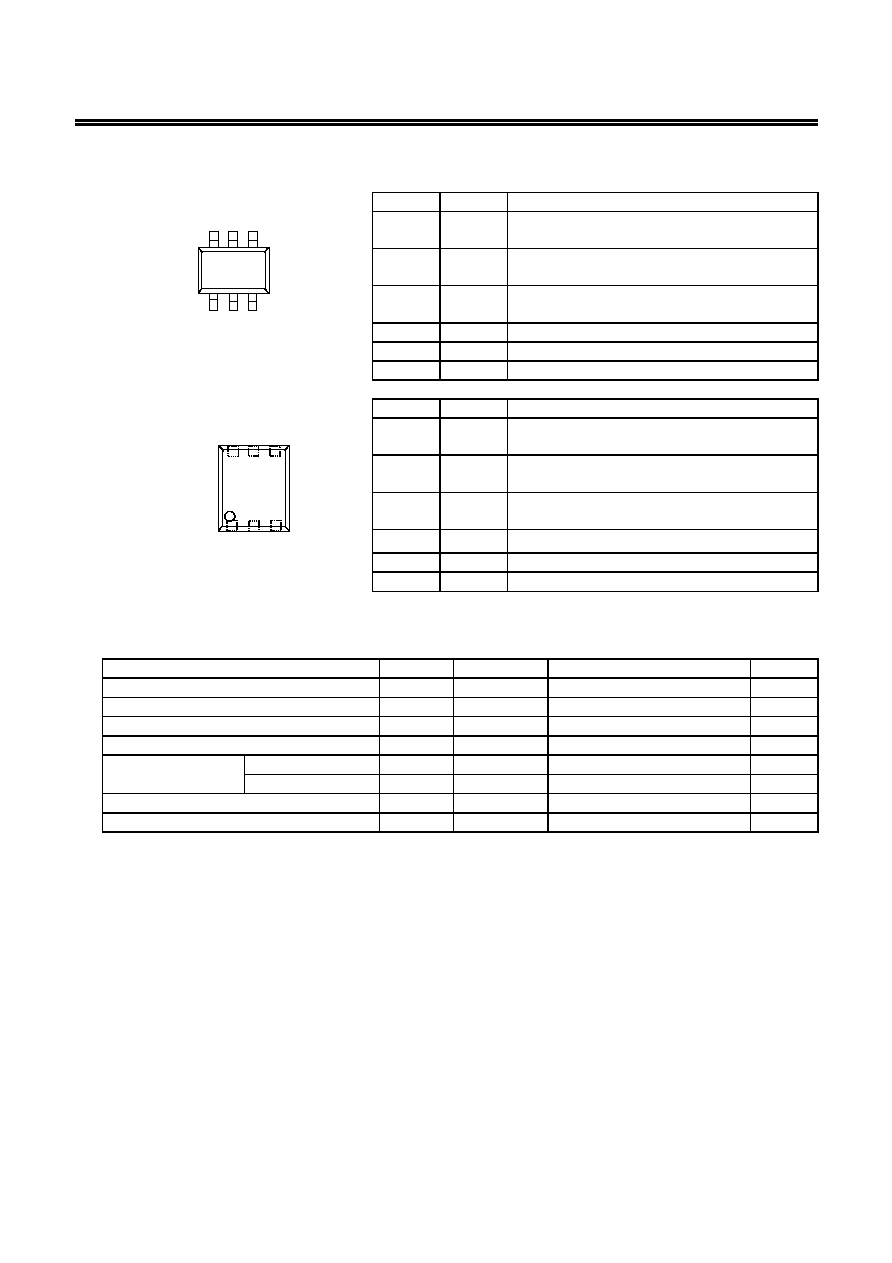
Pin Assignment
Pin
No.
Symbol
Description
1 DO
FET gate control pin for discharge
(CMOS output)
2 VM
Voltage detection pin between VM and VSS
(Overcurrent detection pin)
3 CO
FET gate control pin for charge
(CMOS output)
SOT-23-6
Top view
1 2 3
6 4
5
4
DP
Test pin for delay time measurement
Figure 2
5
VDD
Positive power input pin
6
VSS
Negative power input pin
Pin
No.
Symbol
Description
1 CO
FET gate control pin for charge
(CMOS output)
2 VM
Voltage detection pin between VM and VSS
(Overcurrent detection pin)
3 DO
FET gate control pin for discharge
(CMOS output)
1 2 3
6 4
5
6-Pin SNB(B)
Top view
4
VSS
Negative power input pin
Figure 3
5
DP
Test pin for delay time measurement
6
VDD
Positive power input pin
Absolute Maximum Ratings
(Ta
= 25∞C unless otherwise specified)
Parameter Symbol
Applied
pin
Rating
Unit
Input voltage between VDD and VSS
*1
V
DS
VDD V
SS
-0.3 to V
SS
+12
V
Input pin voltage for VM
V
VM
VM V
DD
-28 to V
DD
+0.3
V
Output pin voltage for CO
V
CO
CO V
VM
-0.3 to V
DD
+0.3
V
Output pin voltage for DO
V
DO
DO V
SS
-0.3 to V
DD
+0.3
V
Power dissipation
SOT-23-6
P
D
250 mW
6-pin
SNB(B)
P
D
90 mW
Operating temperature range
T
opr
-40 to +85
∞C
Storage temperature range
T
stg
-55 to +125
∞C
Caution The absolute maximum ratings are rated values exceeding which the product could
suffer physical damage. These values must therefore not be exceeded under any
conditions.
*1. Do not apply pulse-like noise of
µs order exceeding the above input voltage (V
SS
+12 V). The noise
causes damage to the IC.