Äîêóìåíòàöèÿ è îïèñàíèÿ www.docs.chipfind.ru

Rev.1.9
_00
BATTERY PROTECTION IC FOR SINGLE-CELL PACK
S-8261 Series
Seiko Instruments Inc.
1
The S-8261 series are lithium-ion / lithium polymer
rechargeable battery protection ICs incorporating high-
accuracy voltage detection circuit and delay circuit.
The S-8261 series are suitable for protection of single-cell
lithium ion/lithium polymer battery packs from overcharge,
overdischarge and overcurrent.
Features
(1) Internal high accuracy voltage detection circuit
· Overcharge detection voltage
3.9 V to 4.4 V (applicable in 5 mV step)
Accuracy:
±25 mV (+25 °C) and ±30 mV (-5 °C to +55 °C)
· Overcharge hysteresis voltage
0.0 V to 0.4 V
*1
Accuracy:
±25 mV
The overcharge hysteresis voltage can be selected from the range 0.0 V to 0.4 V in 50 mV step.
· Overdischarge detection voltage 2.0 V to 3.0 V (applicable in 10 mV step) Accuracy: ±50 mV
· Overdischarge hysteresis voltage 0.0 V to 0.7 V
*2
Accuracy:
±50 mV
The overdischarge hysteresis voltage can be selected from the range 0.0 V to 0.7 V in 100 mV step.
· Overcurrent 1 detection voltage 0.05 V to 0.3 V (applicable in 10 mV step) Accuracy: ±15 mV
· Overcurrent 2 detection voltage 0.5 V (fixed) Accuracy: ±100 mV
(2) High voltage device is used for charger connection pins
(VM and CO pins: absolute maximum rating
= 28 V)
(3) Delay times (overcharge: t
CU
, overdischarge: t
DL
, overcurrent 1: t
lOV1
, overcurrent 2: t
lOV2
) are generated
by an internal circuit. No external capacitor is necessary.
Accuracy:
±20%
(4) Three-step overcurrent detection circuit is included.
(overcurrent 1, overcurrent 2 and load short-circuiting)
(5) 0 V battery charge function "available" / "unavailable" are selectable.
(6) Charger detection function and abnormal charge current detection function
· The overdischarge hysteresis is released by detecting negative voltage at the VM pin (-0.7 V typ.).
(Charger detection function)
· When the output voltage of the DO pin is high and the voltage at the VM pin is equal to or lower than
the charger detection voltage (
-0.7 V typ.), the output voltage of the CO pin goes low. (Abnormal
charge current detection function)
(7) Low current consumption
· Operation mode
3.5
µA typ., 7.0 µA max.
· Power-down mode 0.1 µA max.
(8) Wide operating temperature range
-40 °C to +85 °C
(9) Small package SOT-23-6, 6-Pin SNB(B)
*1. Overcharge release voltage
= Overcharge detection voltage - Overcharge hysteresis voltage
(where overcharge release voltage
< 3.8 V is prohibited.)
*2. Overdischarge release voltage
= Overdischarge detection voltage + Overdischarge hysteresis voltage
(where overdischarge release voltage
> 3.4 V is prohibited.)
Applications
· Lithium-ion rechargeable battery packs
· Lithium polymer rechargeable battery packs

BATTERY PROTECTION IC FOR SINGLE-CELL PACK
S-8261 Series
Rev.1.9
_00
Seiko Instruments Inc.
2
Packages
Package name
Drawing code
Package
Tape Reel
SOT-23-6 MP006-A MP006-A MP006-A
6-Pin SNB(B)
BD006-A BD006-A BD006-A
BATTERY PROTECTION IC FOR SINGLE-CELL PACK
Rev.1.9
_00
S-8261 Series
Seiko Instruments Inc.
3
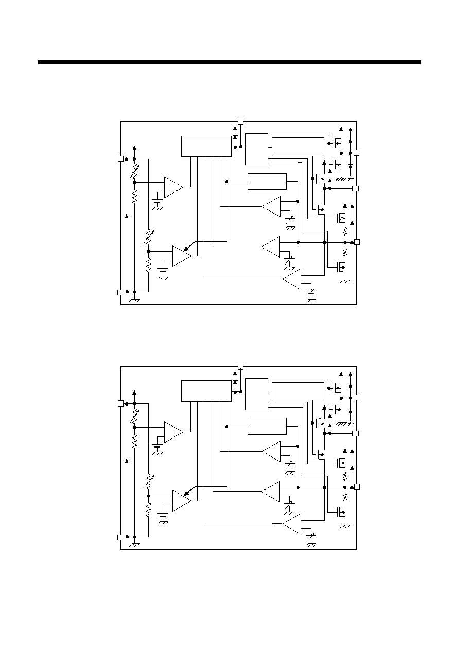
Block Diagrams
1. Product with 0 V Battery Charge Function
+
-
-
+
VM
VSS
VDD
DP
CO
DO
Overcharge
detection
comparator
Overcurrent 2
detection comparator
-
+
-
+
Output control circuit
0 V battery charge
circuit
Overdischarge
detection
comparator
Load short-circuiting
detection comparator
Divider
control
logic
Oscillator control circuit
R
VMD
R
VMS
Charger
detection circuit
Overcurrent 1
detection comparator
-
+
Remark All the diodes shown in the figure are parasitic diodes.
Figure 1
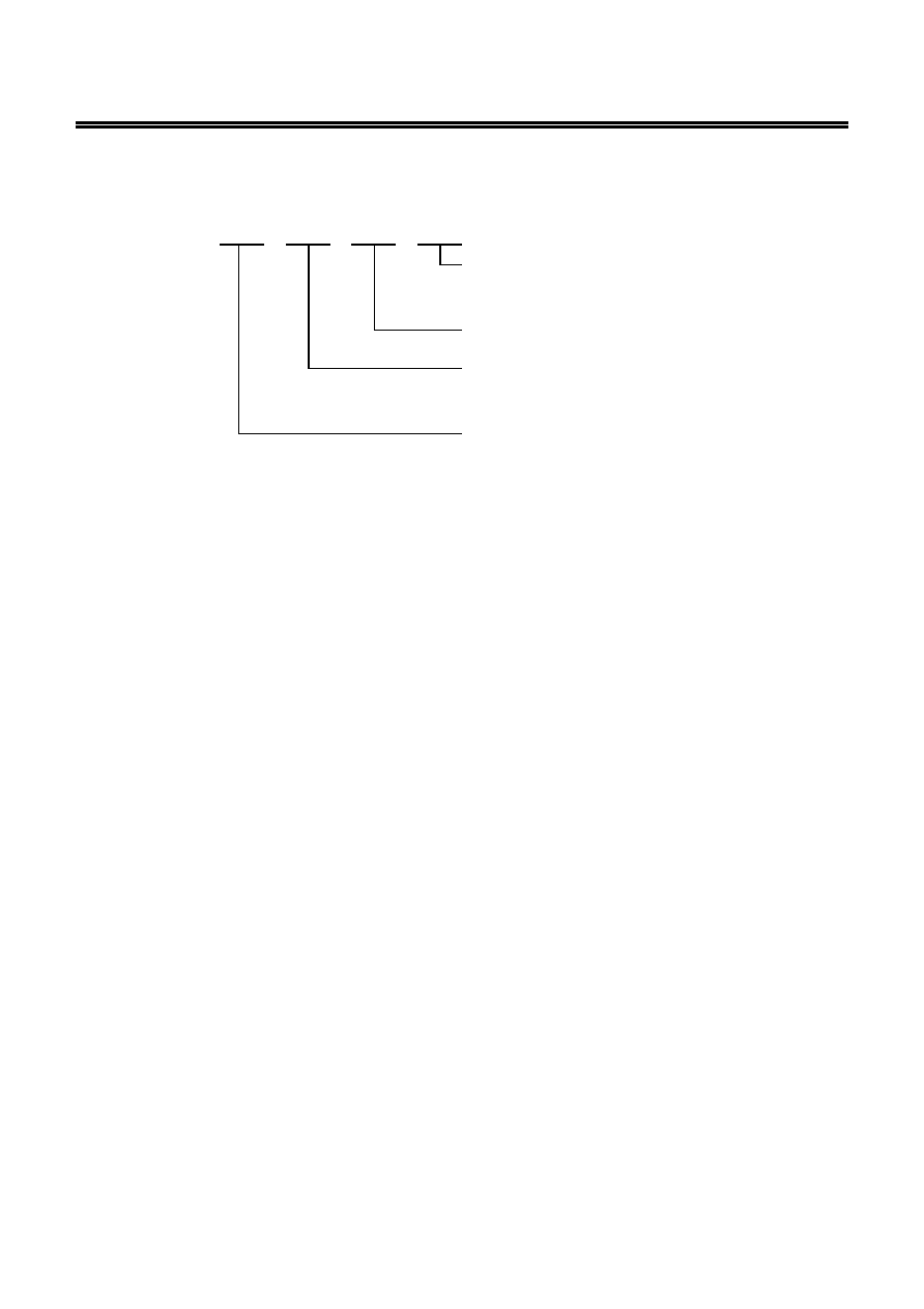
2. Product with 0 V Battery Charge Inhibition Function
+
-
-
+
VM
VSS
VDD
DP
CO
DO
Overcharge
detection
comparator
Overcurrent 2
detection comparator
-
+
-
+
Output control circuit
0 V battery charge
inhibition circuit
Overdischarge
detection
comparator
Load short-circuiting
detection comparator
Divider
control
logic
Oscillator control circuit
R
VMD
R
VMS
Charger
detection circuit
Overcurrent 1
detection comparator
-
+
Remark All the diodes shown in the figure are parasitic diodes.
Figure 2
BATTERY PROTECTION IC FOR SINGLE-CELL PACK
S-8261 Series
Rev.1.9
_00
Seiko Instruments Inc.
4
Product Name Structure
1. Product Name
S
-8261A xx xx - xxx - xx
IC direction in tape specifications
*1
T2: SOT-23-6
TF: 6-Pin SNB(B)
Product name (abbreviation)
*2
Package name (abbreviation)
MD: SOT-23-6
BD: 6-Pin SNB(B)
Serial code
Assigned from AA to ZZ in alphabetical order
*1. Refer to the taping specifications.
*2. Refer to the Product Name List.
BATTERY PROTECTION IC FOR SINGLE-CELL PACK
Rev.1.9
_00
S-8261 Series
Seiko Instruments Inc.
5
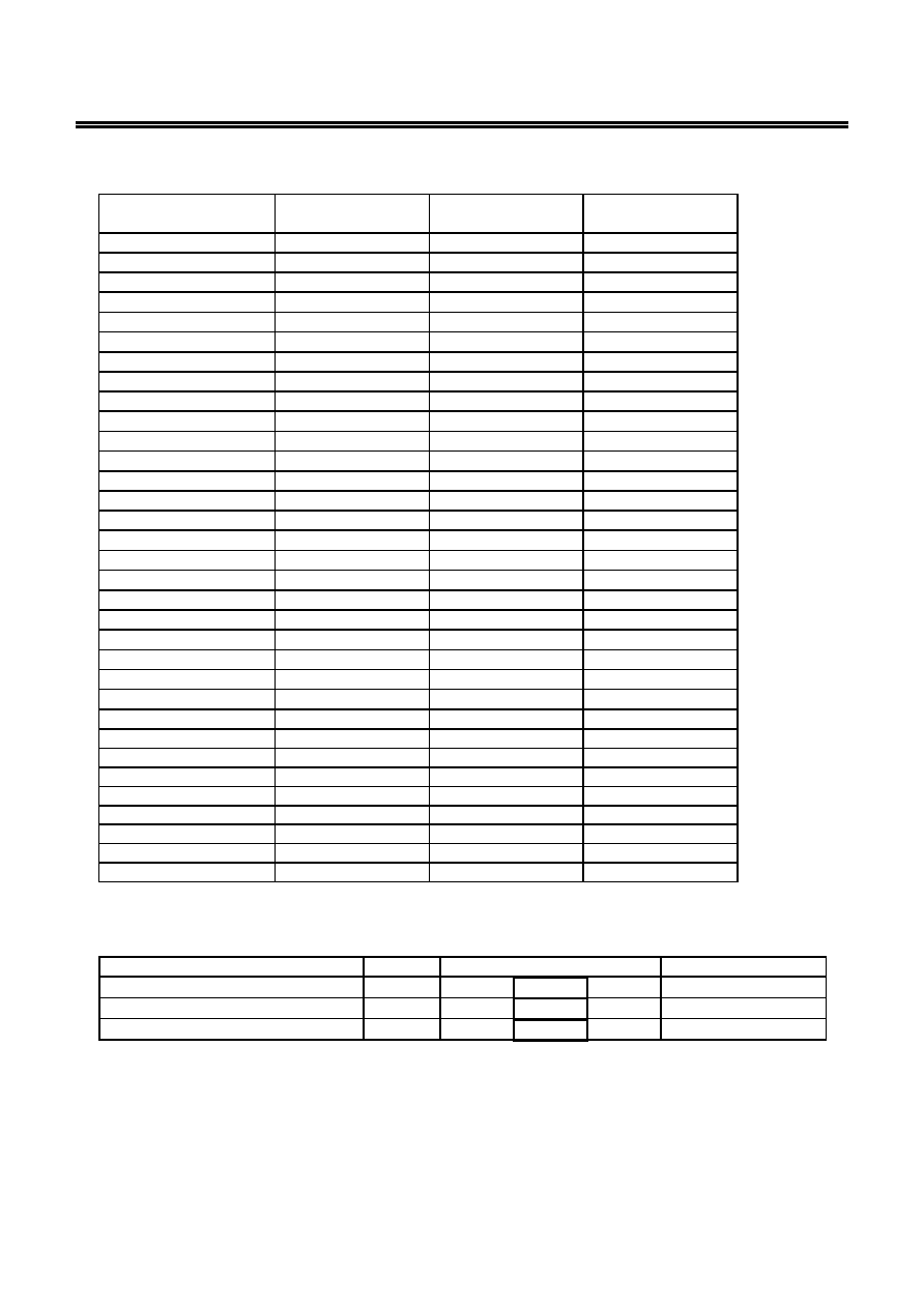
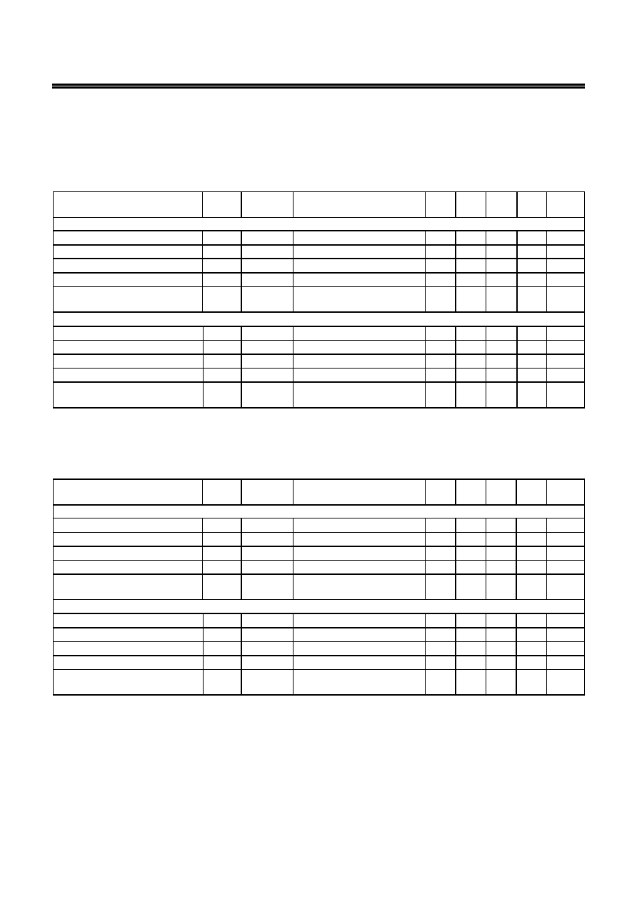
2. Product Name List
Table 1 (1 / 2)
Model No.
Overcharge
detection
voltage [V
CU
]
Overcharge
hysteresis
voltage [V
HC
]
Overdischarge
detection
voltage [V
DL
]
Overdischarge
hysteresis
voltage [V
HD
]
Overcurrent 1
detection
voltage [V
IOV1
]
0 V battery
charge
function
S-8261AAGMD-G2G-T2
4.28 V
0.2 V
2.3 V
0 V
0.16 V
Available
S-8261AAHMD-G2H-T2
4.28 V
0.2 V
2.3 V
0 V
0.08 V
Available
S-8261AAJBD-G2J-TF
4.325 V
0.25 V
2.5 V
0.4 V
0.15 V
Unavailable
S-8261AAJMD-G2J-T2
4.325 V
0.25 V
2.5 V
0.4 V
0.15 V
Unavailable
S-8261AALMD-G2L-T2
4.30 V
0.1 V
2.3 V
0 V
0.08 V
Unavailable
S-8261AAMMD-G2M-T2
4.30 V
0.1 V
2.3 V
0 V
0.2 V
Unavailable
S-8261AANMD-G2N-T2
4.275 V
0.1 V
2.3 V
0.1 V
0.1 V
Available
S-8261AAOMD-G2O-T2
4.28 V
0.2 V
2.3 V
0 V
0.13 V
Unavailable
S-8261AAPMD-G2P-T2
4.325 V
0.25 V
2.5 V
0.4 V
0.1 V
Unavailable
S-8261AARBD-G2R-TF
4.28 V
0.2 V
2.3 V
0 V
0.1 V
Available
S-8261AARMD-G2R-T2
4.28 V
0.2 V
2.3 V
0 V
0.1 V
Available
S-8261AASMD-G2S-T2
4.28 V
0.2 V
2.3 V
0 V
0.15 V
Unavailable
S-8261AAUMD-G2U-T2
4.275 V
0.1 V
2.3 V
0.1 V
0.1 V
Available
S-8261AAVBD-G2V-TF
4.3 V
0.2 V
2.3 V
0 V
0.13 V
Available
S-8261AAXMD-G2X-T2
4.35 V
0.1 V
2.3 V
0.1 V
0.1 V
Available
S-8261AAZMD-G2Z-T2
4.28 V
0.25 V
2.5 V
0.4 V
0.1 V
Unavailable
S-8261ABAMD-G3A-T2
4.35 V
0.2 V
2.5 V
0 V
0.2 V
Available
S-8261ABBMD-G3B-T2
4.275 V
0.2 V
2.3 V
0 V
0.13 V
Available
S-8261ABCMD-G3C-T2
4.30 V
0.2 V
2.3 V
0 V
0.13 V
Available
S-8261ABDBD-G3D-TF
4.28 V
0.2 V
2.3 V
0 V
0.13 V
Available
S-8261ABEBD-G3E-TF
4.275 V
0.2 V
2.3 V
0 V
0.1 V
Available
S-8261ABGBD-G3G-TF
4.275 V
0.2 V
2.3 V
0 V
0.1 V
Unavailable
S-8261ABHBD-G3H-TF
4.20 V
0 V
2.3 V
0 V
0.1 V
Available
S-8261ABIBD-G3I-TF
4.275 V
0.2 V
2.3 V
0 V
0.2 V
Unavailable
S-8261ABJMD-G3J-T2
4.28 V
0.2 V
3.0 V
0 V
0.08 V
Available
S-8261ABKMD-G3K-T2
4.10 V
0.25 V
2.5 V
0.4 V
0.15 V
Unavailable
S-8261ABLBD-G3L-TF
4.275 V
0.2 V
2.3 V
0 V
0.05 V
Unavailable
S-8261ABMMD-G3M-T2
4.28 V
0.2 V
2.8 V
0 V
0.1 V
Available
S-8261ABNMD-G3N-T2
4.30 V
0.2 V
2.3 V
0 V
0.06 V
Available
S-8261ABOBD-G3O-TF
4.28 V
0.2 V
2.3 V
0 V
0.04 V
Available
S-8261ABPMD-G3P-T2
4.20 V
0.1 V
2.8 V
0.1 V
0.15 V
Unavailable
S-8261ABRMD-G3R-T2
4.275 V
0.2 V
2.5 V
0.4 V
0.15 V
Unavailable
S-8261ABSMD-G3S-T2
4.28 V
0.1 V
2.5 V
0.5 V
0.18 V
Unavailable
BATTERY PROTECTION IC FOR SINGLE-CELL PACK
S-8261 Series
Rev.1.9
_00
Seiko Instruments Inc.
6
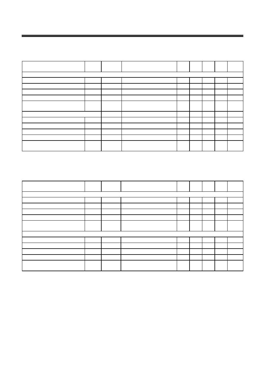
Table 1 (2 / 2)
Model No.
Overcharge
detection delay time
Overdischarge
detection delay time
Overcurrent 1
detection delay time
S-8261AAGMD-G2G-T2
1.2 s
144 ms
9 ms
S-8261AAHMD-G2H-T2
1.2 s
144 ms
9 ms
S-8261AAJBD-G2J-TF
1.2 s
144 ms
9 ms
S-8261AAJMD-G2J-T2
1.2 s
144 ms
9 ms
S-8261AALMD-G2L-T2
1.2 s
144 ms
9 ms
S-8261AAMMD-G2M-T2
1.2 s
144 ms
9 ms
S-8261AANMD-G2N-T2
1.2 s
144 ms
9 ms
S-8261AAOMD-G2O-T2
1.2 s
144 ms
9 ms
S-8261AAPMD-G2P-T2
1.2 s
144 ms
9 ms
S-8261AARBD-G2R-TF
1.2 s
144 ms
9 ms
S-8261AARMD-G2R-T2
1.2 s
144 ms
9 ms
S-8261AASMD-G2S-T2
1.2 s
144 ms
4.5 ms
S-8261AAUMD-G2U-T2
4.6 s
144 ms
9 ms
S-8261AAVBD-G2V-TF
4.6 s
144 ms
9 ms
S-8261AAXMD-G2X-T2
4.6 s
144 ms
9 ms
S-8261AAZMD-G2Z-T2
1.2 s
144 ms
9 ms
S-8261ABAMD-G3A-T2
4.6 s
144 ms
9 ms
S-8261ABBMD-G3B-T2
1.2 s
144 ms
9 ms
S-8261ABCMD-G3C-T2
1.2 s
144 ms
9 ms
S-8261ABDBD-G3D-TF
1.84 s
115 ms
7.2 ms
S-8261ABEBD-G3E-TF
1.2 s
144 ms
9 ms
S-8261ABGBD-G3G-TF
1.2 s
36 ms
9 ms
S-8261ABHBD-G3H-TF
0.3 s
36 ms
18 ms
S-8261ABIBD-G3I-TF
1.2 s
36 ms
9 ms
S-8261ABJMD-G3J-T2
1.2 s
144 ms
9 ms
S-8261ABKMD-G3K-T2
1.2 s
144 ms
9 ms
S-8261ABLBD-G3L-TF
1.2 s
36 ms
9 ms
S-8261ABMMD-G3M-T2
1.2 s
144 ms
9 ms
S-8261ABNMD-G3N-T2
1.2 s
144 ms
9 ms
S-8261ABOBD-G3O-TF
1.2 s
144 ms
9 ms
S-8261ABPMD-G3P-T2
1.2 s
144 ms
9 ms
S-8261ABRMD-G3R-T2
1.2 s
144 ms
9 ms
S-8261ABSMD-G3S-T2
1.2 s
144 ms
9 ms
Remark It is possible to change the detection voltages of the product other than above. The delay times
can also be changed within the range listed bellow. For details, please contact SII marketing
department.
Delay time
Symbol
Selection range
Remarks
Overcharge detection delay time
t
CU
0.15 s
1.2 s
4.6 s
Choose from the left.
Overdischarge detection delay time
t
DL
36 ms
144 ms
290 ms Choose from the left.
Overcurrent 1 detection delay time
t
lOV1
4.5 ms
9 ms
18 ms
Choose from the left.
Remark The values surrounded by bold lines are the delay time of the standard products.
BATTERY PROTECTION IC FOR SINGLE-CELL PACK
Rev.1.9
_00
S-8261 Series
Seiko Instruments Inc.
7
Pin Configurations
Table 2
Pin No.
Symbol
Pin description
1 DO
FET gate control pin for discharge
(CMOS output)
2 VM
Voltage detection pin between VM and VSS
(Overcurrent detection pin)
3 CO
FET gate control pin for charge
(CMOS output)
4
DP
Test pin for delay time measurement
5
VDD
Positive power input pin
6
VSS
Negative power input pin
SOT-23-6
Top view
6
4
5
1 2 3
Figure 3
Table 3
Pin No.
Symbol
Pin description
1 CO
FET gate control pin for charge
(CMOS output)
2 VM
Voltage detection pin between VM and VSS
(Overcurrent detection pin)
3 DO
FET gate control pin for discharge
(CMOS output)
4
VSS
Negative power input pin
5
DP
Test pin for delay time measurement
6
VDD
Positive power input pin
6-Pin
SNB(B)
Top view
6
5
4
1
2
3
4
5
6
3
2
1
Bottom view
*1
*1. Connect the heatsink of back
side at shadowed area to the
board, and set electric
potential open or VDD.
However, do not use it
as
the function of electrode.
Figure 4
BATTERY PROTECTION IC FOR SINGLE-CELL PACK
S-8261 Series
Rev.1.9
_00
Seiko Instruments Inc.
8
Absolute Maximum Ratings
Table 4
(Ta
= 25 °C unless otherwise specified)
Parameter Symbol
Applied
pin
Rating
Unit
Input voltage between VDD and VSS
*1
V
DS
VDD V
SS
-0.3 to V
SS
+12
V
Input pin voltage for VM
V
VM
VM V
DD
-28 to V
DD
+0.3
V
Output pin voltage for CO
V
CO
CO V
VM
-0.3 to V
DD
+0.3
V
Output pin voltage for DO
V
DO
DO V
SS
-0.3 to V
DD
+0.3
V
Power dissipation
SOT-23-6
P
D
250 mW
6-pin
SNB(B)
P
D
90 mW
Operating temperature range
T
opr
-40 to +85
°C
Storage temperature range
T
stg
-55 to +125
°C
Caution The absolute maximum ratings are rated values exceeding which the product could suffer
physical damage. These values must therefore not be exceeded under any conditions.
*1. Even pulse (
µs) noise exceeding the above input voltage (V
SS
+ 12 V) may damage the IC, so do not
allow such noise to be applied.
BATTERY PROTECTION IC FOR SINGLE-CELL PACK
Rev.1.9
_00
S-8261 Series
Seiko Instruments Inc.
9
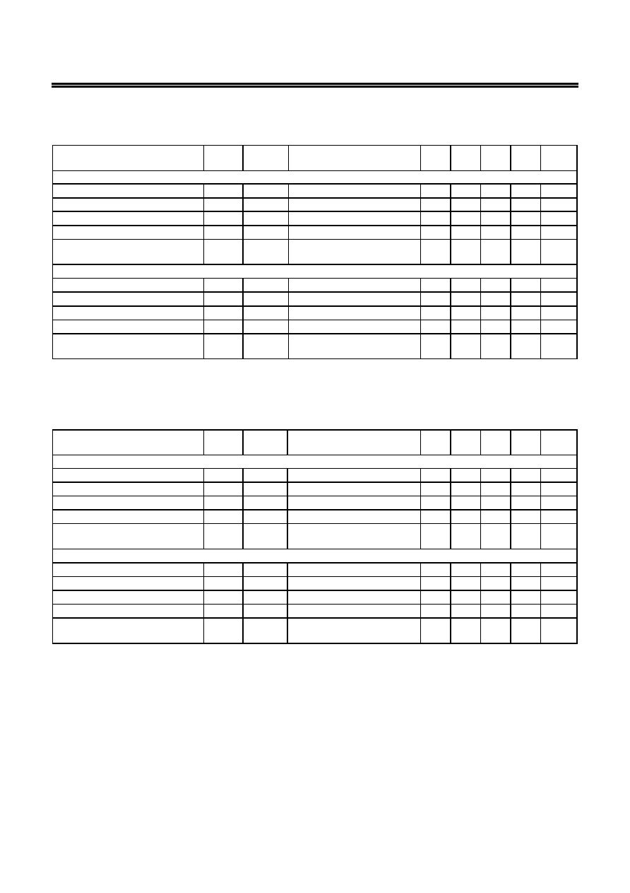
Electrical Characteristics
1. Except Detection Delay Time (25
°C)
Table 5
(Ta
= 25 °C unless otherwise specified)
Parameter Symbol
Test
condition
Remark Min.
Typ.
Max.
Unit
Test
circuit
[DETECTION VOLTAGE]
Overcharge detection voltage
V
CU
= 3.9 V to 4.4 V, 5 mV Step
V
CU
1
V
CU
-0.025
V
CU
V
CU
+0.025
V 1
Ta
= -5 °C to 55 °C
*1
V
CU
-0.030
V
CU
V
CU
+0.030
Overcharge hysteresis voltage
V
HC
= 0.0 V to 0.4 V, 50 mV Step
V
HC
1
V
HC
-0.025
V
HC
V
HC
+0.025
V 1
Overdischarge detection voltage
V
DL
= 2.0 V to 3.0 V, 10 mV Step
V
DL
2
V
DL
-0.050
V
DL
V
DL
+0.050
V 2
Overdischarge hysteresis voltage
V
HD
= 0.0 V to 0.7 V, 100 mV Step
V
HD
2
V
HD
-0.050
V
HD
V
HD
+0.050
V 2
Overcurrent 1 detection voltage
V
IOV1
= 0.05 V to 0.3 V, 10 mV Step
V
IOV1
3
V
IOV1
-0.015
V
IOV1
V
IOV1
+0.015
V 2
Overcurrent 2 detection voltage
V
IOV2
3
0.4 0.5 0.6 V 2
Load short-circuiting detection
voltage
V
SHORT
3
0.9 1.2 1.5 V 2
Charger detection voltage
V
CHA
4
-1.0 -0.7 -0.4
V 2
[INPUT VOLTAGE, OPERATION VOLTAGE]
Operation voltage between VDD
and VSS
V
DSOP1
Internal circuit operating voltage
1.5
8 V
Operation voltage between VDD
and VM
V
DSOP2
Internal circuit operating voltage
1.5
28 V
[CURRENT CONSUMPTION]
Current consumption in normal
operation
I
OPE
5
V
DD
= 3.5 V, V
VM
= 0 V
1.0 3.5 7.0
µA
2
Current consumption at power
down
I
PDN
5
V
DD
= V
VM
= 1.5 V
0.1
µA
2
[OUTPUT RESISTANCE]
CO pin resistance "H"
R
COH
7
V
CO
= 3.0 V, V
DD
= 3.5 V, V
VM
= 0 V
2.5 5 10 k
4
CO pin resistance "L"
R
COL
7
V
CO
= 0.5 V, V
DD
= 4.5 V, V
VM
= 0 V
2.5 5 10 k
4
DO pin resistance "H"
R
DOH
8
V
DO
= 3.0 V, V
DD
= 3.5 V, V
VM
= 0 V
2.5 5 10 k
4
DO pin resistance "L"
R
DOL
8
V
DO
= 0.5 V, V
DD
= V
VM
= 1.8 V
2.5 5 10 k
4
[VM INTERNAL RESISTANCE]
Internal resistance between VM
and VDD
R
VMD
6
V
DD
= 1.8 V, V
VM
= 0 V
100 300 900 k
3
Internal resistance between VM
and VSS
R
VMS
6
V
DD
= 3.5 V, V
VM
= 1.0 V
10 20 40 k
3
[0 V BATTERY CHARGING FUNCTION]
0 V battery charge starting charger
voltage
V
0CHA
11
0 V battery charging available
1.2
V 2
0 V battery charge inhibition battery
voltage
V
0INH
12
0 V battery charging unavailable
0.5 V 2
*1. Since products are not screened at high and low temperatures, the specification for this temperature range
is guaranteed by design, not tested in production.
BATTERY PROTECTION IC FOR SINGLE-CELL PACK
S-8261 Series
Rev.1.9
_00
Seiko Instruments Inc.
10
2. Except Detection Delay Time (
-40 to +85 °C
*1
)
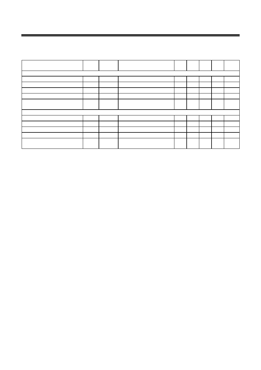
Table 6
(Ta
= -40 to +85 °C
*1
unless otherwise specified)
Parameter Symbol
Test
condition
Remark Min.
Typ.
Max.
Unit
Test
circuit
[DETECTION VOLTAGE]
Overcharge detection voltage
V
CU
= 3.9 V to 4.4 V, 5 mV Step
V
CU
1
V
CU
-0.055
V
CU
V
CU
+0.040
V 1
Overcharge hysteresis voltage
V
HC
= 0.0 V to 0.4 V, 50 mV Step
V
HC
1
V
HC
-0.025
V
HC
V
HC
+0.025
V 1
Overdischarge detection voltage
V
DL
= 2.0 V to 3.0 V, 10 mV Step
V
DL
2
V
DL
-0.080
V
DL
V
DL
+0.080
V 2
Overdischarge hysteresis voltage
V
HD
= 0.0 V to 0.7 V, 100 mV Step
V
HD
2
V
HD
-0.050
V
HD
V
HD
+0.050
V 2
Overcurrent 1 detection voltage
V
IOV1
= 0.05 V to 0.3 V, 10 mV Step
V
IOV1
3
V
IOV1
-0.021
V
IOV1
V
IOV1
+0.021
V 2
Overcurrent 2 detection voltage
V
IOV2
3
0.37 0.5 0.63 V 2
Load short-circuiting detection
voltage
V
SHORT
3
0.7 1.2 1.7 V 2
Charger detection voltage
V
CHA
4
-1.2 -0.7 -0.2
V 2
[INPUT VOLTAGE, OPERATION VOLTAGE]
Operation voltage between VDD
and VSS
V
DSOP1
Internal circuit operating voltage
1.5
8 V
Operation voltage between VDD
and VM
V
DSOP2
Internal circuit operating voltage
1.5
28 V
[CURRENT CONSUMPTION]
Current consumption in normal
operation
I
OPE
5
V
DD
= 3.5 V, V
VM
= 0 V
0.7 3.5 8.0
µA
2
Current consumption at power
down
I
PDN
5
V
DD
= V
VM
= 1.5 V
0.1
µA
2
[OUTPUT RESISTANCE]
CO pin resistance "H"
R
COH
7
V
CO
= 3.0 V, V
DD
= 3.5 V, V
VM
= 0 V
1.2 5 15 k
4
CO pin resistance "L"
R
COL
7
V
CO
= 0.5 V, V
DD
= 4.5 V, V
VM
= 0 V
1.2 5 15 k
4
DO pin resistance "H"
R
DOH
8
V
DO
= 3.0 V, V
DD
= 3.5 V, V
VM
= 0 V
1.2 5 15 k
4
DO pin resistance "L"
R
DOL
8
V
DO
= 0.5 V, V
DD
= V
VM
= 1.8 V
1.2 5 15 k
4
[VM INTERNAL RESISTANCE]
Internal resistance between VM
and VDD
R
VMD
6
V
DD
= 1.8 V, V
VM
= 0 V
78 300 1310 k
3
Internal resistance between VM
and VSS
R
VMS
6
V
DD
= 3.5 V, V
VM
= 1.0 V
7.2 20 44 k
3
[0 V BATTERY CHARGING FUNCTION]
0 V battery charge starting charger
voltage
V
0CHA
11
0 V battery charging available
1.7
V 2
0 V battery charge inhibition battery
voltage
V
0INH
12
0 V battery charging unavailable
0.3 V 2
*1. Since products are not screened at high and low temperatures, the specification for this temperature range
is guaranteed by design, not tested in production.
BATTERY PROTECTION IC FOR SINGLE-CELL PACK
Rev.1.9
_00
S-8261 Series
Seiko Instruments Inc.
11
3. Detection Delay Time
Table 7
S-8261AAG, S-8261AAH, S-8261AAJ, S-8261AAL, S-8261AAM, S-8261AAN, S-8261AAO, S-8261AAP,
S-8261AAR, S-8261AAZ, S-8261ABB, S-8261ABC, S-8261ABE, S-8261ABJ, S-8261ABK, S-8261ABM,
S-8261ABN, S-8261ABO, S-8261ABP, S-8261ABR, S-8261ABS
Parameter Symbol
Test
condition
Remark Min.
Typ.
Max.
Unit
Test
circuit
[DELAY TIME] 25 °C
Overcharge detection delay time
t
CU
9
0.96 1.2 1.4 s
5
Overdischarge detection delay time
t
DL
9
115 144 173 ms 5
Overcurrent 1 detection delay time
t
lOV1
10
7.2 9 11 ms 5
Overcurrent 2 detection delay time
t
lOV2
10
1.8 2.24 2.7 ms 5
Load short-circuiting detection delay
time
t
SHORT
10
220 320 380
µs
5
[DELAY TIME]
-40 °C to +85 °C
*1
Overcharge detection delay time
t
CU
9
0.7 1.2 2.0 s 5
Overdischarge detection delay time
t
DL
9
80 144 245 ms 5
Overcurrent 1 detection delay time
t
lOV1
10
5 9 15
ms 5
Overcurrent 2 detection delay time
t
lOV2
10
1.2 2.24 3.8 ms 5
Load short-circuiting detection delay
time
t
SHORT
10
150 320 540
µs
5
*1. Since products are not screened at high and low temperatures, the specification for this temperature range
is guaranteed by design, not tested in production.
Table 8
S-8261AAS
Parameter Symbol
Test
condition
Remark Min.
Typ.
Max.
Unit
Test
circuit
[DELAY TIME] 25 °C
Overcharge detection delay time
t
CU
9
0.96 1.2 1.4 s
5
Overdischarge detection delay time
t
DL
9
115 144 173 ms 5
Overcurrent 1 detection delay time
t
lOV1
10
3.6 4.5 5.4 ms 5
Overcurrent 2 detection delay time
t
lOV2
10
1.8 2.24 2.7 ms 5
Load short-circuiting detection delay
time
t
SHORT
10
220 320 380
µs
5
[DELAY TIME]
-40 °C to +85 °C
*1
Overcharge detection delay time
t
CU
9
0.7 1.2 2.0 s 5
Overdischarge detection delay time
t
DL
9
80 144 245 ms 5
Overcurrent 1 detection delay time
t
lOV1
10
2.5 4.5 7.7 ms 5
Overcurrent 2 detection delay time
t
lOV2
10
1.2 2.24 3.8 ms 5
Load short-circuiting detection delay
time
t
SHORT
10
150 320 540
µs
5
*1. Since products are not screened at high and low temperatures, the specification for this temperature range
is guaranteed by design, not tested in production.
BATTERY PROTECTION IC FOR SINGLE-CELL PACK
S-8261 Series
Rev.1.9
_00
Seiko Instruments Inc.
12
Table 9
S-8261AAU, S-8261AAX, S-8261ABA
Parameter Symbol
Test
condition
Remark Min.
Typ.
Max.
Unit
Test
circuit
[DELAY TIME] 25 °C
Overcharge detection delay time
t
CU
9
3.7 4.6 5.5 s 5
Overdischarge detection delay time
t
DL
9
115 144 173 ms 5
Overcurrent 1 detection delay time
t
lOV1
10
7.2 9 11 ms 5
Overcurrent 2 detection delay time
t
lOV2
10
1.8 2.24 2.7 ms 5
Load short-circuiting detection delay
time
t
SHORT
10
220 320 380
µs
5
[DELAY TIME]
-40 °C to +85 °C
*1
Overcharge detection delay time
t
CU
9
2.5 4.6 7.8 s 5
Overdischarge detection delay time
t
DL
9
80 144 245 ms 5
Overcurrent 1 detection delay time
t
lOV1
10
5 9 15
ms 5
Overcurrent 2 detection delay time
t
lOV2
10
1.2 2.24 3.8 ms 5
Load short-circuiting detection delay
time
t
SHORT
10
150 320 540
µs
5
*1. Since products are not screened at high and low temperatures, the specification for this temperature range
is guaranteed by design, not tested in production.
Table 10
S-8261AAV
Parameter Symbol
Test
condition
Remark Min.
Typ.
Max.
Unit
Test
circuit
[DELAY TIME] 25 °C
Overcharge detection delay time
t
CU
9
3.7 4.6 5.5 s 5
Overdischarge detection delay time
t
DL
9
115 144 173 ms 5
Overcurrent 1 detection delay time
t
lOV1
10
7.2 9 11 ms 5
Overcurrent 2 detection delay time
t
lOV2
10
3.6 4.5 5.4 ms 5
Load short-circuiting detection delay
time
t
SHORT
10
450 600 720
µs
5
[DELAY TIME]
-40 °C to +85 °C
*1
Overcharge detection delay time
t
CU
9
2.5 4.6 7.8 s 5
Overdischarge detection delay time
t
DL
9
80 144 245 ms 5
Overcurrent 1 detection delay time
t
lOV1
10
5 9 15
ms 5
Overcurrent 2 detection delay time
t
lOV2
10
2.5 4.5 7.7 ms 5
Load short-circuiting detection delay
time
t
SHORT
10
310 600 1020
µs
5
*1. Since products are not screened at high and low temperatures, the specification for this temperature range
is guaranteed by design, not tested in production.
BATTERY PROTECTION IC FOR SINGLE-CELL PACK
Rev.1.9
_00
S-8261 Series
Seiko Instruments Inc.
13
Table 11
S-8261ABD
Parameter Symbol
Test
condition
Remark Min.
Typ.
Max.
Unit
Test
circuit
[DELAY TIME] 25°C
Overcharge detection delay time
t
CU
9
1.48 1.84 2.2 s
5
Overdischarge detection delay time
t
DL
9
92 115 138 ms 5
Overcurrent 1 detection delay time
t
lOV1
10
5.76 7.2 8.8 ms 5
Overcurrent 2 detection delay time
t
lOV2
10
2.88 3.6 4.32 ms 5
Load short-circuiting detection delay
time
t
SHORT
10
358 488 586
µs
5
[DELAY TIME]
-40°C to +85°C
*1
Overcharge detection delay time
t
CU
9
1.11 1.84 2.89 s
5
Overdischarge detection delay time
t
DL
9
68.9 115 182.3 ms 5
Overcurrent 1 detection delay time
t
lOV1
10
4.31 7.2 11.59 ms 5
Overcurrent 2 detection delay time
t
lOV2
10
2.16 3.6 5.68 ms 5
Load short-circuiting detection delay
time
t
SHORT
10
268 488 770
µs
5
*1. Since products are not screened at high and low temperatures, the specification for this temperature range
is guaranteed by design, not tested in production.
Table 12
S-8261ABG, S-8261ABI, S-8261ABL
Parameter Symbol
Test
condition
Remark Min.
Typ.
Max.
Unit
Test
circuit
[DELAY TIME] 25°C
Overcharge detection delay time
t
CU
9
0.96 1.2 1.4 s
5
Overdischarge detection delay time
t
DL
9
29 36 43 ms 5
Overcurrent 1 detection delay time
t
lOV1
10
7.2 9 11 ms 5
Overcurrent 2 detection delay time
t
lOV2
10
1.8 2.24 2.7 ms 5
Load short-circuiting detection delay
time
t
SHORT
10
220 320 380
µs
5
[DELAY TIME]
-40°C to +85°C
*1
Overcharge detection delay time
t
CU
9
0.7 1.2 2.0 s 5
Overdischarge detection delay time
t
DL
9
20 36 61 ms 5
Overcurrent 1 detection delay time
t
lOV1
10
5 9 15
ms 5
Overcurrent 2 detection delay time
t
lOV2
10
1.2 2.24 3.8 ms 5
Load short-circuiting detection delay
time
t
SHORT
10
150 320 540
µs
5
*1. Since products are not screened at high and low temperatures, the specification for this temperature range
is guaranteed by design, not tested in production.
BATTERY PROTECTION IC FOR SINGLE-CELL PACK
S-8261 Series
Rev.1.9
_00
Seiko Instruments Inc.
14
Table 13
S-8261ABH
Parameter Symbol
Test
condition
Remark Min.
Typ.
Max.
Unit
Test
circuit
[DELAY TIME] 25°C
Overcharge detection delay time
t
CU
9
0.24 0.3 0.36 s
5
Overdischarge detection delay time
t
DL
9
29 36 43 ms 5
Overcurrent 1 detection delay time
t
lOV1
10
14 18 22 ms 5
Overcurrent 2 detection delay time
t
lOV2
10
1.8 2.24 2.7 ms 5
Load short-circuiting detection delay
time
t
SHORT
10
220 320 380
µs
5
[DELAY TIME]
-40°C to +85°C
*1
Overcharge detection delay time
t
CU
9
0.17 0.3 0.51 s
5
Overdischarge detection delay time
t
DL
9
20 36 61 ms 5
Overcurrent 1 detection delay time
t
lOV1
10
10 18 31 ms 5
Overcurrent 2 detection delay time
t
lOV2
10
1.2 2.24 3.8 ms 5
Load short-circuiting detection delay
time
t
SHORT
10
150 320 540
µs
5
*1. Since products are not screened at high and low temperatures, the specification for this temperature range
is guaranteed by design, not tested in production.

BATTERY PROTECTION IC FOR SINGLE-CELL PACK
Rev.1.9
_00
S-8261 Series
Seiko Instruments Inc.
15
Test Circuits
Remark Unless otherwise specified, the output voltage levels "H" and "L" at CO pin (V
CO
) and DO pin (V
DO
) are
judged by the threshold voltage (1.0 V) of the N-channel FET. Judge the CO pin level with respect to
V
VM
and the DO pin level with respect to V
SS
.
(1) Test Condition 1, Test Circuit 1
Overcharge Detection Voltage, Overcharge Hysteresis Voltage
The overcharge detection voltage (V
CU
) is defined by the voltage between VDD and VSS at which V
CO
goes
from "H" to "L" when the voltage V1 is gradually increased from the starting condition of V1
= 3.5 V. The
overcharge hysteresis voltage (V
HC
) is then defined as the difference between the overcharge detection
voltage (V
CU
) and the voltage between VDD and VSS at which V
CO
goes from "H" to "L" when the voltage V1
is gradually decreased.
(2) Test Condition 2, Test Circuit 2
Overdischarge Detection Voltage, Overdischarge Hysteresis Voltage
The overdischarge detection voltage (V
DL
) is defined as the voltage between VDD and VSS at which V
DO
goes from "H" to "L" when the voltage V1 is gradually decreased from the starting condition of V1
= 3.5 V and
V2
= 0 V. The overdischarge hysteresis voltage (V
HD
) is then defined as the difference between the
overdischarge detection voltage (V
DL
) and the voltage between VDD and VSS at which V
DO
goes from "H" to
"L" when the voltage V1 is gradually increased.
(3) Test Condition 3, Test Circuit 2
Overcurrent 1 Detection Voltage, Overcurrent 2 Detection Voltage, Load Short-Circuiting Detection
Voltage
The overcurrent 1 detection voltage (V
IOV1
) is defined as the voltage between VM and VSS whose delay time
for changing V
DO
from "H" to "L" lies between the minimum and the maximum value of the overcurrent 1
detection delay time when the voltage V2 is increased rapidly (within 10
µs) from the starting condition V1 =
3.5 V and V2
= 0 V.
The overcurrent 2 detection voltage (V
IOV2
) is defined as the voltage between VM and VSS whose delay time
for changing V
DO
from "H" to "L" lies between the minimum and the maximum value of the overcurrent 2
detection delay time when the voltage V2 is increased rapidly (within 10
µs) from the starting condition V1 =
3.5 V and V2
= 0 V.
The load short-circuiting detection voltage (V
SHORT
) is defined as the voltage between VM and VSS whose
delay time for changing V
DO
from "H" to "L" lies between the minimum and the maximum value of the load
short-circuiting detection delay time when the voltage V2 is increased rapidly (within 10
µs) from the starting
condition V1
= 3.5 V and V2 = 0 V.
(4) Test Condition 4, Test Circuit 2
Charger Detection Voltage, Abnormal Charge Current Detection Voltage
The charger detection voltage (V
CHA
) is defined as the voltage between VM and VSS at which V
DO
goes from
"L" to "H" when the voltage V3 is gradually decreased from 0 V after the voltage V1 is gradually increased
from the starting condition of V1
= 1.8 V and V2 = 0 V until the voltage V1 becomes V1 = V
DL
+ (V
HD
/ 2).
The charger detection voltage can be measured only in the product whose overdischarge hysteresis V
HD
0.
Set V1
= 3.5 V and V2 = 0 V. Decrease V2 from 0 V gradually. The voltage between VM and VSS when
V
CO
goes from "H" to "L" is the abnormal charge current detection voltage. The abnormal charge current
detection voltage has the same value as the charger detection voltage (V
CHA
).
(5) Test Condition 5, Test Circuit 2
Normal Operation Current Consumption, Power-Down Current Consumption
The operating current consumption (I
OPE
) is the current that flows through the VDD pin (I
DD
) under the set
conditions of V1
= 3.5 V and V2 = 0 V (Normal condition).
The power-down current consumption (I
PDN
) is the current that flows through the VDD pin (I
DD
) under the set
conditions of V1
= V2 = 1.5 V (Overdischarge condition).

BATTERY PROTECTION IC FOR SINGLE-CELL PACK
S-8261 Series
Rev.1.9
_00
Seiko Instruments Inc.
16
(6) Test Condition 6, Test Circuit 3
Internal Resistance between VM and VDD, Internal Resistance between VM and VSS
The resistance between VM and VDD (R
VMD
) is the internal resistance between VM and VDD under the set
conditions of V1
= 1.8 V and V2 = 0 V.
The resistance between VM and VSS (R
VMS
) is the internal resistance between VM and VDD under the set
conditions of V1
= 3.5 V and V2 = 1.0 V.
(7) Test Condition 7, Test Circuit 4
CO Pin Resistance "H", CO Pin Resistance "L"
The CO pin resistance "H" (R
COH
) is the resistance t the CO pin under the set condition of V1
= 3.5 V, V2 =
0 V and V3
= 3.0 V.
The CO pin resistance "L" (R
COL
) is the resistance t the CO pin under the set condition of V1
= 4.5 V, V2 = 0 V
and V3
= 0.5 V.
(8) Test Condition 8, Test Circuit 4
DO Pin Resistance "H", DO Pin Resistance "L"
The DO pin resistance "H" (R
DOH
) is the resistance t the DO pin under the set condition of V1
= 3.5 V, V2 =
0 V and V4
= 3.0 V.
The DO pin resistance "L" (R
DOL
) is the resistance t the DO pin under the set condition of V1
= 1.8 V, V2 = 0 V
and V4
= 0.5 V.
(9) Test Condition 9, Test Circuit 5
Overcharge Detection Delay Time, Overdischarge Detection Delay Time
The overcharge detection delay time (t
CU
) is the time needed for V
CO
to change from "H" to "L" just after the
voltage V1 momentarily increases (within 10
µs) from the overcharge detection voltage (V
CU
)
- 0.2 V to the
overcharge detection voltage (V
CU
)
+ 0.2 V under the set condition of V2 = 0 V.
The overdischarge detection delay time (t
DL
) is the time needed for V
DO
to change from "H" to "L" just after the
voltage V1 momentarily decreases (within 10
µs) from the overdischarge detection voltage (V
DL
)
+0.2 V to the
overdischarge detection voltage (V
DL
)
- 0.2 V under the set condition of V2 = 0 V.
(10) Test Condition 10, Test Circuit 5
Overcurrent 1 Detection Delay Time, Overcurrent 2 Detection Delay Time, Load Short-circuiting
Detection Delay Time, Abnormal Charge Current Detection Delay Time
The overcurrent 1 detection delay time (t
IOV1
) is the time needed for V
DO
to go "L" after the voltage V2
momentarily increases (within 10
µs) from 0 V to 0.35 V under the set condition of V1 = 3.5 V and V2=0 V.
The overcurrent 2 detection delay time (t
IOV2
) is the time needed for V
DO
to go "L" after the voltage V2
momentarily increases (within 10
µs) from 0 V to 0.7 V under the set condition of V1 = 3.5 V and V2 = 0 V.
The load short-circuiting detection delay time (t
SHORT
) is the time needed for V
DO
to go "L" after the voltage V2
momentarily increases (within 10
µs) from 0 V to 1.6 V under the set condition of V1 = 3.5 V and V2 = 0 V.
The abnormal charge current detection delay time is the time needed for V
CO
to go from "H" to "L" after the
voltage V2 momentarily decreases (within 10
µs) from 0 V to -1.1 V under the set condition of V1 = 3.5 V and
V2
= 0 V. The abnormal charge current detection delay time has the same value as the overcharge detection
delay time.
(11) Test Condition 11, Test Circuit 2 (Product with 0 V battery charge function)
0 V Battery Charge Starting Charger Voltage
The 0 V battery charge starting charger voltage (V
0CHA
) is defined as the voltage between VDD and VM at
which V
CO
goes "H" (V
VM
+ 0.1 V or higher) when the voltage V2 is gradually decreased from the starting
condition of V1
= V2 = 0 V.
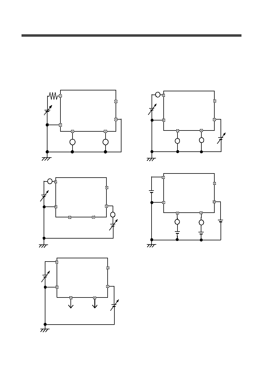
BATTERY PROTECTION IC FOR SINGLE-CELL PACK
Rev.1.9
_00
S-8261 Series
Seiko Instruments Inc.
17
(12) Test Condition 12, Test Circuit 2 (Product with 0 V battery charge inhibition function)
0 V Battery Charge Inhibition Battery Voltage
The 0 V battery charge inhibition battery voltage (V
0INH
) is defined as the voltage between VDD and VSS at
which V
CO
goes "H" (V
VM
+ 0.1 V or higher) when the voltage V1 is gradually increased from the starting
condition of V1
= 0 V and V2 = -4 V.
VSS
DO
CO
VDD
S-8261 series
R1
= 470
V1
DP
VM
Test Circuit 1
V
DO
COM
V
CO
V
V
A
COM
V2
V
V
V
CO
VM
DO
CO
DP
VSS
V1
V
DO
VDD
I
DD
S-8261 series
Test Circuit 2
A
COM
V2
VM
CO
DO
DP
VSS
V1
VDD
I
DD
S-8261 series
I
VM
A
Test Circuit 3
A
A
V4
V3
V2
I
CO
DP
VM
DO
CO
COM
VSS
V1
VDD
I
DO
S-8261 series
Test Circuit 4
V2
COM
VM
CO
DO
DP
VSS
V1
VDD
Oscilloscope
S-8261 series
Oscilloscope
Test Circuit 5
Figure 5

BATTERY PROTECTION IC FOR SINGLE-CELL PACK
S-8261 Series
Rev.1.9
_00
Seiko Instruments Inc.
18
Operation
Remark Refer to the "Battery Protection IC Connection Example".
1. Normal Condition
The S-8261 Series monitors the voltage of the battery connected between VDD pin and VSS pin and the
voltage difference between VM pin and VSS pin to control charging and discharging. When the battery
voltage is in the range from the overdischarge detection voltage (V
DL
) to the overcharge detection voltage
(V
CU
), and the VM pin voltage is in the range from the charger detection voltage (V
CHA
) to the overcurrent
1 detection voltage (V
IOV1
), the IC turns both the charging and discharging control FETs on. This
condition is called the normal condition, and in this condition charging and discharging can be carried out
freely.
Remark When a battery is connected to the IC for the first time, discharging may not be enabled. In
this case, short the VM pin and VSS pin or connect the charger to restore the normal
condition.
2. Overcurrent Condition (Detection of Overcurrent 1, Overcurrent 2 and Load Short-circuiting)
When a battery in the normal status is in the status where the voltage of the VM pin is equal to or higher
than the overcurrent detection voltage because the discharge current is higher than the specified value
and the status lasts for the overcurrent detection delay time, the discharge control FET is turned off and
discharging is stopped. This status is called the overcurrent status.
In the overcurrent status, the VM and VSS pins are shorted by the resistor between VM and VSS (R
VMS
)
in the IC. However, the voltage of the VM pin is at the V
DD
potential due to the load as long as the load
is connected. When the load is disconnected, the VM pin returns to the V
SS
potential.
This IC detects the status when the impedance between the EB
+ pin and EB- pin (Refer to Figure 11)
increases and is equal to the impedance that enables automatic restoration and the voltage at the VM pin
returns to overcurrent detection voltage 1 (V
IOV1
) or lower and the overcurrent status is restored to the
normal status.
Remark The impedance that enables automatic restoration varies depending on the battery voltage and
the set value of overcurrent 1 detection voltage.
3. Overcharge Condition
When the battery voltage becomes higher than the overcharge detection voltage (V
CU
) during charging
under the normal condition and the detection continues for the overcharge detection delay time (t
CU
) or
longer, the S-8261 Series turns the charging control FET off to stop charging. This condition is called
the overcharge condition.
The overcharge condition is released by the following two cases ((1) and (2)):
(1) When the battery voltage falls below the overcharge release voltage (V
CU
)
- overcharge detection
hysteresis voltage (V
HC
), the S-8261 Series turns the charging control FET on and turns to the normal
condition.
(2) When a load is connected and discharging starts, the S-8261 Series turns the charging control FET
on and returns to the normal condition. Just after the load is connected and discharging starts, the
discharging current flows through the parasitic diode in the charging control FET. At this moment the
VM pin potential becomes V
f
, the voltage for the parasitic diode, higher than V
SS
level. When the
battery voltage goes under the overcharge detection voltage (V
CU
) and provided that the VM pin
voltage is higher than the overcurrent 1 detection voltage, the S-8261 Series releases the overcharge
condition.
Remark 1. If the battery is charged to a voltage higher than the overcharge detection voltage (V
CU
) and
the battery voltage does not fall below the overcharge detection voltage (V
CU
) even when a
heavy load is connected, the detection of overcurrent 1, overcurrent 2 and load short-
circuiting do not function until the battery voltage falls below over charge detection voltage
(V
CU
). Since an actual battery has an internal impedance of several dozens of m
, the
battery voltage drops immediately after a heavy load that causes overcurrent is connected,
and the detection of overcurrent 1, overcurrent 2 and load short-circuiting function.
2. When a charger is connected after the overcharge detection, the overcharge condition is
not released even if the battery voltage is below the overcharge release voltage (V
CL
).
The overcharge condition is released when the VM pin voltage goes over the charger
detection voltage (V
CHA
) by removing the charger.

BATTERY PROTECTION IC FOR SINGLE-CELL PACK
Rev.1.9
_00
S-8261 Series
Seiko Instruments Inc.
19
4. Overdischarge Condition
When the battery voltage falls below the overdischarge detection voltage (V
DL
) during discharging under
the normal condition and the detection continues for the overdischarge detection delay time (t
DL
) or
longer, the S-8261 Series turns the discharging control FET off to stop discharging. This condition is
called the overdischarge condition. When the discharging control FET is turned off, the VM pin voltage
is pulled up by the resistor between VM and VDD in the IC (R
VMD
). When the voltage difference between
the VM and VDD then is 1.3 V (typ.) or lower, the current consumption is reduced to the power-down
current consumption (I
PDN
). This condition is called the power-down condition.
The power-down condition is released when a charger is connected and the voltage difference between
the VM and VDD becomes 1.3 V (typ.) or higher. Moreover when the battery voltage becomes the
overdischarge detection voltage (V
DL
) or higher, the S-8261 Series turns the discharging FET on and
returns to the normal condition.
5. Charger Detection
When a battery in the overdischarge condition is connected to a charger and provided that the VM pin
voltage is lower than the charger detection voltage (V
CHA
), the S-8261 Series releases the overdischarge
condition and turns the discharging control FET on when the battery voltage becomes equal to or higher
than the overdischarge detection voltage (V
DL
) since the charger detection function works. This action is
called charger detection.
When a battery in the overdischarge condition is connected to a charger and provided that the VM pin
voltage is not lower than the charger detection voltage (V
CHA
), the S-8261 Series releases the
overdischarge condition when the battery voltage reaches the overdischarge detection voltage (V
DL
)
+
overdischarge hysteresis (V
HD
) or higher.
6. Abnormal Charge Current Detection
If the VM pin voltage falls below the charger detection voltage (V
CHA
) during charging under normal
condition and it continues for the overcharge detection delay time (t
CU
) or longer, the charging control
FET turns off and charging stops. This action is called the abnormal charge current detection.
Abnormal charge current detection works when the DO pin voltage is "H" and the VM pin voltage falls
below the charger detection voltage (V
CHA
). Consequently, if an abnormal charge current flows to an
over-discharged battery, the S-8261 Series turns the charging control FET off and stops charging after
the battery voltage becomes higher than the overdischarge detection voltage which make the DO pin
voltage "H", and still after the overcharge detection delay time (t
CU
) elapses.
Abnormal charge current detection is released when the voltage difference between VM pin and VSS pin
becomes less than charger detection voltage (V
CHA
).
BATTERY PROTECTION IC FOR SINGLE-CELL PACK
S-8261 Series
Rev.1.9
_00
Seiko Instruments Inc.
20
7. Delay Circuits
The detection delay times are determined by dividing a clock of the approximately 3.5 kHz with the
counter.
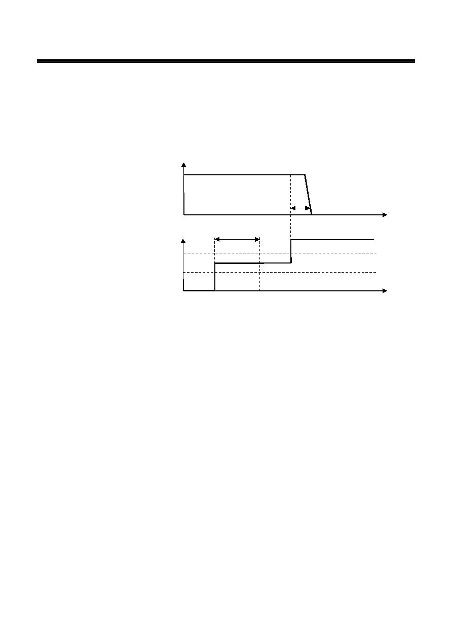
Remark 1. The detection delay time for overcurrent 2 (t
IOV2
) and load short-circuiting (t
SHORT
) start when
the overcurrent 1 (V
IOV1
) is detected. When the overcurrent 2 (V
IOV2
) or load short-circuiting
(V
SHORT
) is detected over the detection delay time for each of them (= t
IOV2
or t
SHORT
) after the
detection of overcurrent 1 (V
IOV1
), the S-8261 Series turns the FET off within t
IOV2
or t
SHORT
of
each detection.
DO pin
VM pin
V
DD
V
DD
Time
V
IOV1
V
SS
V
SS
V
IOV2
Overcurrent 2 detection delay time (t
IOV2
)
Time
t
D
0t
D
t
IOV2
Figure 6
2. When the overcurrent is detected and continues for longer than the overdischarge detection
delay time (t
DL
) without releasing the load, the condition changes to the power-down condition
when the battery voltage falls below the overdischarge detection voltage (V
DL
). When the
battery voltage falls below the overdischarge detection voltage (V
DL
) due to the overcurrent,
the S-8261 Series turns the discharging control FET off by the overcurrent detection. In this
case the recovery of the battery voltage is so slow that if the battery voltage after the
overdischarge detection delay time (t
DL
) is still lower than the over discharge detection
voltage (V
DL
), the S-8261 Series shifts to the power-down condition.
8. DP Pin
The DP pin is a test pin for delay time measurement and it should be open in the actual application. If a
capacitor whose capacitance is larger than 1000 pF or a resister whose resistance is less than 1 M
is
connected to this pin, error may occur in the delay times or in the detection voltages.
9. 0 V Battery Charging Function "Available"
This function is used to recharge the connected battery whose voltage is 0 V due to the self-discharge.
When the 0 V battery charge starting charger voltage (V
0CHA
) or higher is applied between EB
+ pin and
EB
- pin by connecting a charger, the charging control FET gate is fixed to VDD pin voltage. When the
voltage between the gate and source of the charging control FET becomes equal to or higher than the
turn-on voltage due to the charger voltage, the charging control FET is turned on to start charging. At
this time, the discharging control FET is off and the charging current flows through the internal parasitic
diode in the discharging control FET. When the battery voltage becomes equal to or higher than the
overdischarge release voltage (V
DU
), the S-8261 Series enters the normal condition.
Caution Some battery providers do not recommend charging for completely self-discharged
battery. Please ask battery providers before determine whether to enable or inhibit the
0 V battery charging function.
Remark The 0 V battery charge function has higher priority than the abnormal charge current detection
function. Consequently, a product with the 0 V battery charging function is enabled charges
a battery forcibly and abnormal charge current cannot be detected when the battery voltage is
low.

BATTERY PROTECTION IC FOR SINGLE-CELL PACK
Rev.1.9
_00
S-8261 Series
Seiko Instruments Inc.
21
10. 0 V Battery Charging Function "Unavailable"
This function inhibits the recharging when a battery that is short-circuited (0 V battery) internally is
connected. When the battery voltage is the 0 V battery charge inhibition battery voltage (V
0INH
) or lower,
the charging control FET gate is fixed to EB
- pin voltage to inhibit charging. When the battery voltage is
the 0 V battery charge inhibition battery voltage (V
0INH
) or higher, charging can be performed.
Caution Some battery providers do not recommend charging for completely self-discharged
battery. Please ask battery providers before determining the 0 V battery charging
function.
BATTERY PROTECTION IC FOR SINGLE-CELL PACK
S-8261 Series
Rev.1.9
_00
Seiko Instruments Inc.
22
Operation Timing Chart
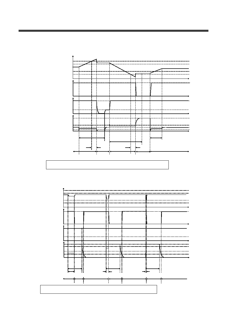
1. Overcharge and Overdischarge Detection
V
DL
+V
HD
V
DL
V
DD
V
SS
(2)
(1)
(1)
(1)
(3)
Battery
voltage
DO pin
CO pin
VM pin
Charger connection
Load connection
Mode
Overdischarge detection delay time (t
DL
)
Remark (1) Normal condition, (2) Overcharge condition, (3) Overdischarge condition, (4) Overcurrent condition
The charger is supposed to charge with constant current.
Overcharge detection delay time (t
CU
)
V
DD
V
DD
V
IOV1
V
SS
V
CHA
V
SS
V
CU
V
CU
V
HC
Figure
7
2. Overcurrent Detection
V
CU
V
CU
-V
HC
V
DL
+V
HD
V
DL
V
DD
V
SS
V
DD
V
SS
(1)
(4)
(1)
(4)
(1)
(4)
(1)
V
DD
V
SHORT
V
IOV2
V
IOV1
V
SS
Overcurrent 1 detection delay time (t
IOV1
)
Overcurrent 2 detection delay time (t
IOV2
)
Load short-circuiting detection delay time (t
SHORT
)
Battery
voltage
DO pin
CO pin
VM pin
Charger connection
Load connection
Mode
Remark (1) Normal condition, (2) Overcharge condition, (3) Overdischarge condition, (4) Overcurrent condition
The charger is supposed to charge with constant current.
Figure
8
BATTERY PROTECTION IC FOR SINGLE-CELL PACK
Rev.1.9
_00
S-8261 Series
Seiko Instruments Inc.
23
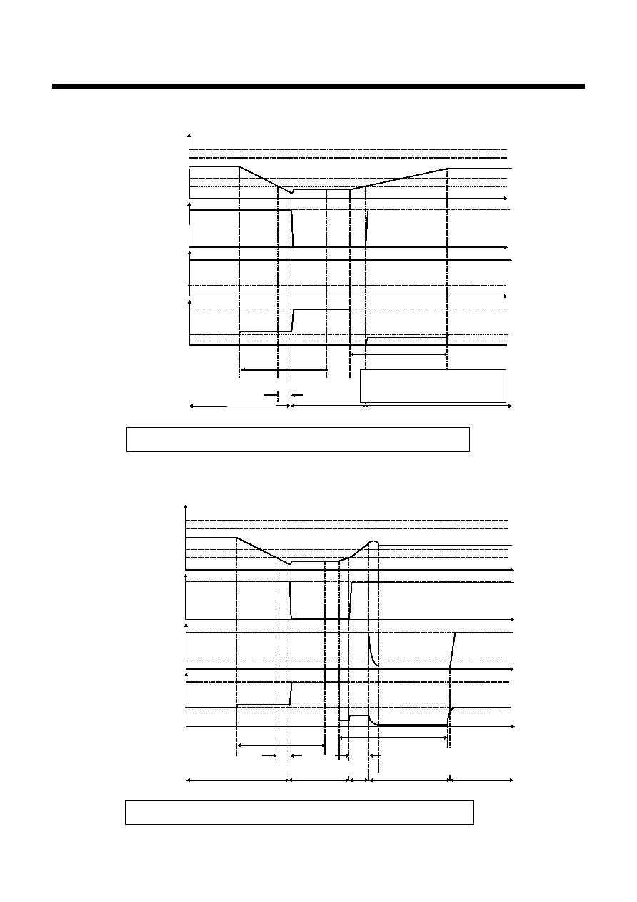
3. Charger Detection
V
CU
V
CU
-V
HC
V
DL
+V
HD
V
DL
V
DD
V
SS
V
DD
V
SS
V
DD
V
SS
V
CHA
Overdischarge detection delay time (t
DL
)
In case VM pin voltage
< V
CHA
Overdischarge is released at the overdischarge
detection voltage (V
DL
)
(1)
(3)
(1)
Battery
voltage
DO pin
CO pin
VM pin
Charger connection
Load connection
Mode
Remark (1) Normal condition, (2) Overcharge condition, (3) Overdischarge condition, (4) Overcurrent condition
The charger is supposed to charge with constant current.
Figure 9
4. Abnormal Charge Current Detection
Abnormal charging current detection delay time
(
= Overcharge detection delay time (t
CU
))
Overdischarge detection delay time (t
DL
)
(3) (1)
(2)
(1)
(1)
Battery
voltage
DO pin
CO pin
VM pin
Charger connection
Load connection
Mode
Remark (1) Normal condition, (2) Overcharge condition, (3) Overdischarge condition, (4) Overcurrent condition
The charger is supposed to charge with constant current.
V
CU
V
CU
-V
HC
V
DL
+V
HD
V
DL
V
DD
V
SS
V
DD
V
SS
V
DD
V
SS
V
CHA
Figure 10
BATTERY PROTECTION IC FOR SINGLE-CELL PACK
S-8261 Series
Rev.1.9
_00
Seiko Instruments Inc.
24
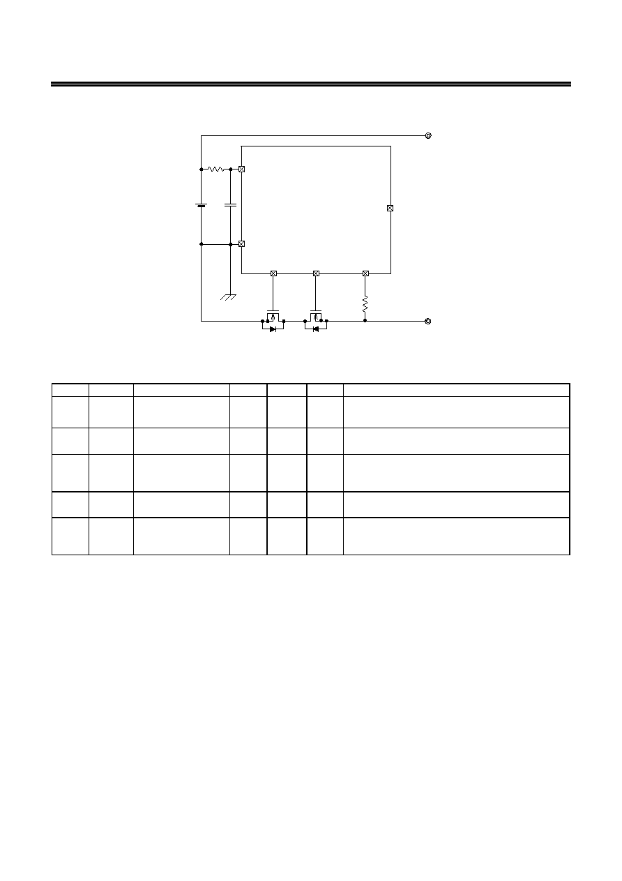
Battery Protection IC Connection Example
EB
+
EB
-
S-8261 Series
470
VSS
Battery
DO
VDD
R2
2 k
C1
CO VM
FET1
FET2
R1
0.1
µF
DP
Figure 11
Table 14 Constant for External Components
Symbol Part
Purpose
Typ. Min. Max.
Remarks
FET1
N-channel
MOS FET
Discharge control
Threshold voltage
Overdischarge detection voltage
*1
Gate to source withstanding voltage
Charger voltage
*2
FET2
N-channel
MOS FET
Charge control
Threshold voltage
Overdischarge detection voltage
*1
Gate to source withstanding voltage
Charger voltage
*2
R1 Resistor
ESD protection,
For power fluctuation
470
300
1
k
Resistance should be as small as possible to avoid
lowering of the overcharge detection accuracy caused
by VDD pin current.
*3
C1
Capacitor For power fluctuation
0.1
µF 0.022 µF 1.0 µF
Install a capacitor of 0.022
µF or higher between VDD
and VSS.
*4
R2 Resistor
Protection for reverse
connection of a charger 2 k 300
4
k
Select as large a resistance as large as possible to
prevent current when a charger is connected in
reverse.
*5
*1. If the threshold voltage of an FET is low, the FET may not cut the charging current.
If an FET with a threshold voltage equal to or higher than the overdischarge detection voltage is used,
discharging may be stoped before overdischarge is detected.
*2. If the withstanding voltage between the gate and source is lower than the charger voltage, the FET may
be destroyed.
*3. If R1 has a high resistance, the voltage between VDD and VSS may exceed the absolute maximum
rating when a charger is connected in reverse since the current flows from the charger to the IC. Insert a
resistor of 300
or higher to R1 for ESD protection.
*4. If a capacitor of less than 0.022
µF is connected to C1, DO may oscillate when load short-circuiting is
detected. Be sure to connect a capacitor of 0.022
µF or higher to C1.
*5. If R2 has a resistance higher than 4 k
, the charging current may not be cut when a high-voltage charger
is connected.

BATTERY PROTECTION IC FOR SINGLE-CELL PACK
Rev.1.9
_00
S-8261 Series
Seiko Instruments Inc.
25
Caution1. The above constants may be changed without notice.
2. The DP pin should be open.
3. It has not been confirmed whether the operation is normal or not in circuits other than the
above example of connection. In addition, the example of connection shown above and the
constant do not guarantee proper operation. Perform through evaluation using the actual
application to set the constant.
Precautions
· The application conditions for the input voltage, output voltage, and load current should not exceed the
package power dissipation.
· Do not apply an electrostatic discharge to this IC that exceeds the performance ratings of the built-in
electrostatic protection circuit.
· SII claims no responsibility for any and all disputes arising out of or in connection with any infringement by
products including this IC of patents owned by a third party.

BATTERY PROTECTION IC FOR SINGLE-CELL PACK
S-8261 Series
Rev.1.9
_00
Seiko Instruments Inc.
26
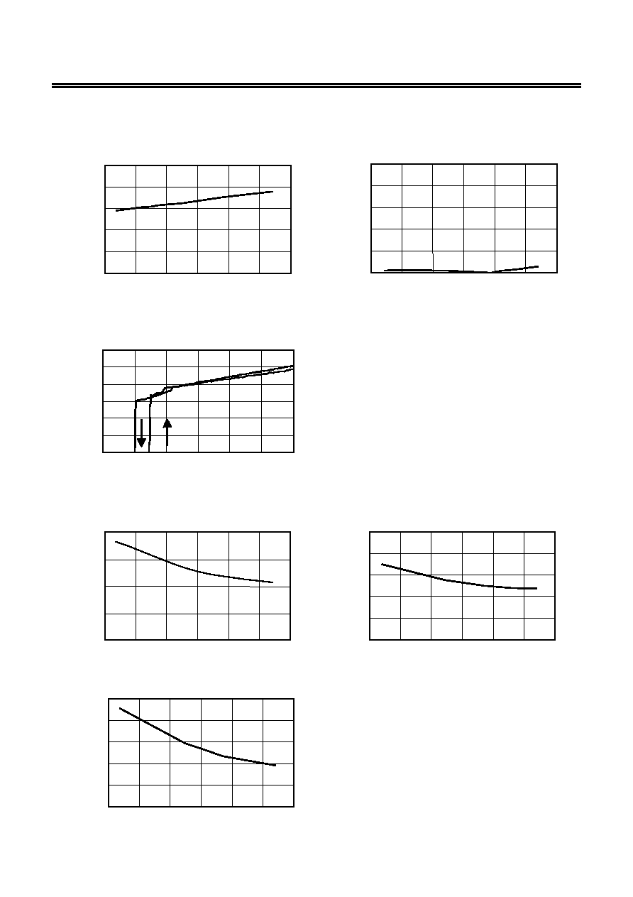
Characteristics (Typical Data)
1. Detection / Release Voltage Temperature Characteristics
Overcharge detection voltage vs. temperature
Overcharge release voltage vs. temperature
4.34
4.36
4.38
4.40
4.42
4.44
-25 0 25 50 75
Ta [°C]
V
CU
[V
]
-50 100
3.92
3.94
3.96
3.98
4.00
4.02
-25
0
25 50 75
Ta [°C]
V
CL
[V
]
-50
100
Overdischarge detection voltage vs. temperature
Overdischarge release voltage vs. temperature
2.94
2.96
2.98
3.00
3.02
3.04
-25 0 25 50 75
Ta [°C]
V
DL
[V
]
-50 100
3.34
3.36
3.38
3.40
3.42
3.44
-25
0
25 50 75
Ta [°C]
V
DU
[V]
-50
100
Overcurrent 1 detection voltage vs. temperature
Overcurrent 2 detection voltage vs. temperature
0.15
0.20
0.25
0.30
0.35
0.40
0.45
-25 0 25 50 75
Ta [°C]
V
IOV1
[
V
]
-50 100
0.40
0.45
0.50
0.55
0.60
0.65
-25
0
25 50 75
Ta [°C]
V
IOV2
[V
]
-50
100
Load short-circuiting detection voltage vs.temperature
1.0
1.1
1.2
1.3
1.4
1.5
-25 0 25 50 75
Ta [°C]
V
SHORT
[V]
-50 100
BATTERY PROTECTION IC FOR SINGLE-CELL PACK
Rev.1.9
_00
S-8261 Series
Seiko Instruments Inc.
27
2. Current Consumption Temperature Characteristics
Current consumption vs. temperature in normal
mode
Current consumption vs. temperature in power-down
mode
0
1
2
3
4
5
-25 0 25 50 75
Ta [°C]
I
OPE
[
µ
A]
-50 100
0
0.02
0.04
0.06
0.08
0.10
-25
0
25 50 75
Ta [°C]
I
PDN
[
µ
A]
-50
100
3. Current Consumption Power Voltage Characteristics (Ta
=25°C)
Current consumption power supply voltage dependency
0
1
2
3
4
5
6
0 2 4 6 8 10
12
V
DD
[V]
I
OPE
[
µ
A]
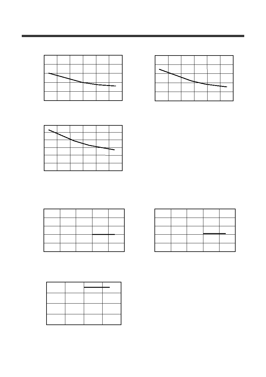
4. Detection / Release Delay Time Temperature Characteristics
Overcharge detection delay time vs. temperature
Overcharge release delay time vs. temperature
0.50
0.75
1.00
1.25
1.50
-
25 0 25 50 75
Ta [°C]
t
CU
[
s]
-
50 100
10
20
30
40
50
60
-25
0
25 50 75
Ta [°C]
t
CL
[m
s
]
-50
100
Overdischarge detection delay time vs. temperature
100
120
140
160
180
200
-25 0 25 50 75
Ta [°C]
t
DL
[m
s
]
-50 100
BATTERY PROTECTION IC FOR SINGLE-CELL PACK
S-8261 Series
Rev.1.9
_00
Seiko Instruments Inc.
28
Overcurrent 1 detection delay time vs. temperature
Overcurrent 2 detection delay time vs. temperature
5
7
9
11
13
15
-25 0 25 50 75
Ta [°C]
t
IOV1
[ms
]
-50 100
1.4
1.8
2.2
2.6
3.0
3.4
-25
0
25 50 75
Ta [°C]
t
IOV2
[m
s
]
-50
100
Load short-circuiting delay time vs. temperature
0.16
0.20
0.24
0.28
0.32
0.36
0.40
-25
0 25 50 75
Ta [°C]
t
SHORT
[ms
]
-50
100
5. Delay Time Power-Voltage Characteristics (Ta
=25°C)
Overcurrent 1 detection delay time vs. power supply
voltage dependency
Overcurrent 2 detection delay time vs. power supply
voltage dependency
5
7
9
11
13
15
2 2.5 3 3.5 4 4.5
V
DD
[V]
t
IOV1
[V
]
1.4
1.8
2.2
2.6
3.0
3.4
2
2.5
3 3.5 4
4.5
V
DD
[V]
t
IO
V2
[m
s
]
Load short-circuiting delay time vs. power supply
voltage dependency
0.16
0.2
0.24
0.28
0.32
2.5 3 3.5 4 4.5
V
DD
[V]
t
SH
O
R
T
[m
s
]
BATTERY PROTECTION IC FOR SINGLE-CELL PACK
Rev.1.9
_00
S-8261 Series
Seiko Instruments Inc.
29
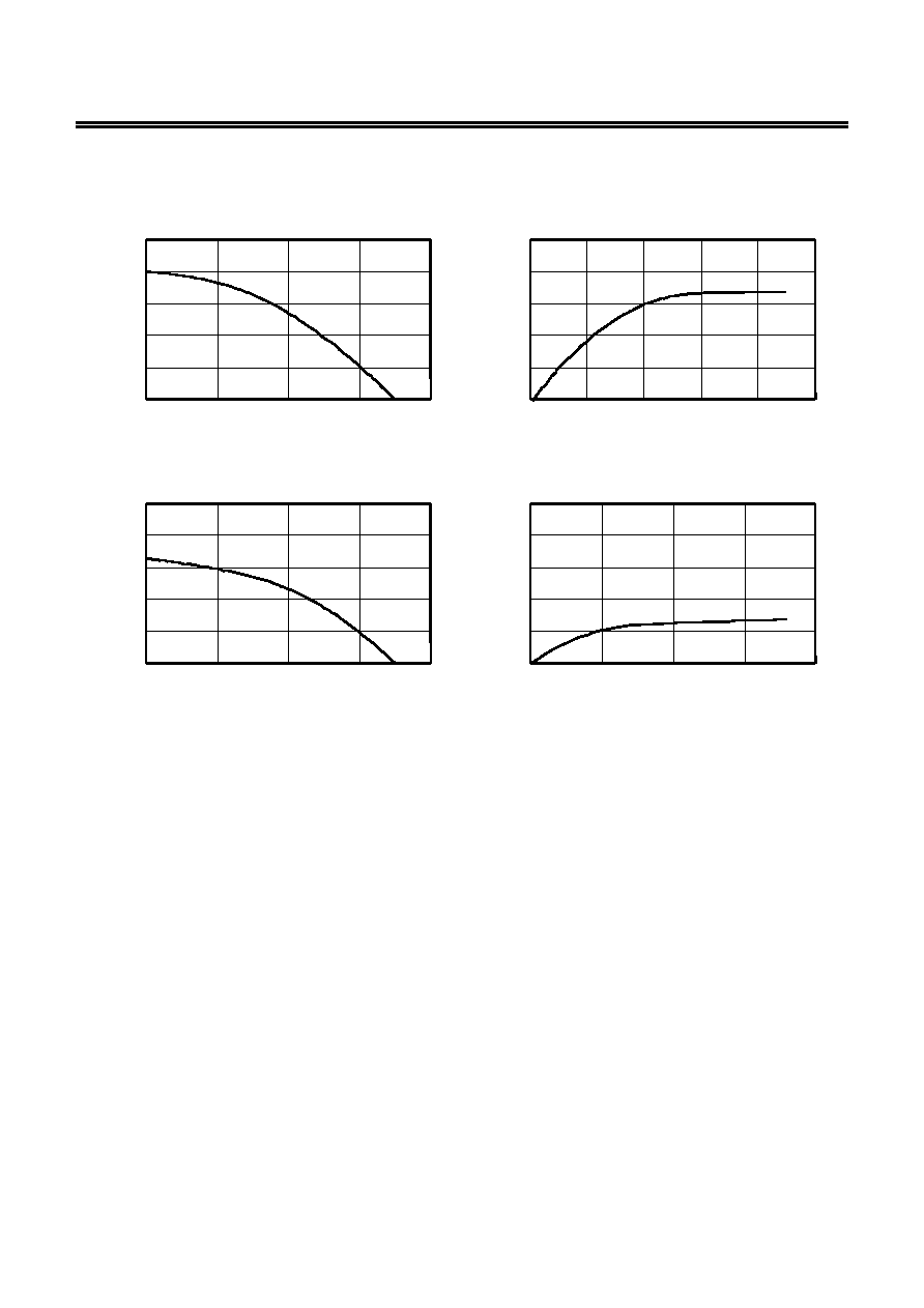
6. CO Pin / DO Pin Output Current Characteristics (Ta
= 25°C)
CO pin source current characteristics
V
DD
= 3.5 V, V
M
= V
SS
= 0 V
CO pin sink current characteristics
V
DD
= 4.5 V, V
M
= V
SS
= 0 V
-0.5
-0.4
-0.3
-0.2
-0.1
0
0 1 2 3 4
V
CO
[V]
I
CO
[mA]
0.5
0.4
0.3
0.2
0.1
0
0
1
2
3
5
V
CO
[V]
I
CO
[mA]
4
DO pin source current characteristics
V
DD
= 3.5 V, V
M
= V
SS
= 0 V
DO pin sink current characteristics
V
DD
= 1.8 V, V
M
= V
SS
= 0 V
-0.5
-0.4
-0.3
-0.2
-0.1
0
0 1 2 3 4
V
DO
[V]
I
DO
[mA]
0.5
0.4
0.3
0.2
0.1
0
0
0.5
1
2
V
DO
[V]
I
DO
[mA]
1.5
2.9±0.2
0.15
1.9±0.2
1
2
3
4
6
5
0.35±0.15
0.95
+0.1
-0.05
0.95
No.
TITLE
SCALE
UNIT
mm
Seiko Instruments Inc.
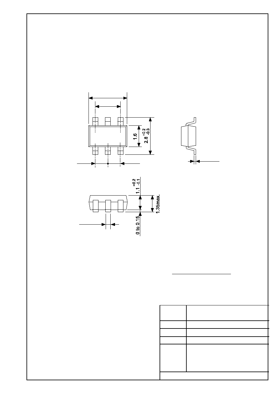
No. MP006-A-P-SD-1.1
MP006-A-P-SD-1.1
SOT236-A-PKG Dimensions
No.
TITLE
SCALE
UNIT
mm
1
2
3
4 5 6
ø1.5
+0.1
-0
2.0±0.05
ø1.0
+0.2
-0
4.0±0.1
1.4±0.2
0.25±0.1
3.2±0.2
Seiko Instruments Inc.
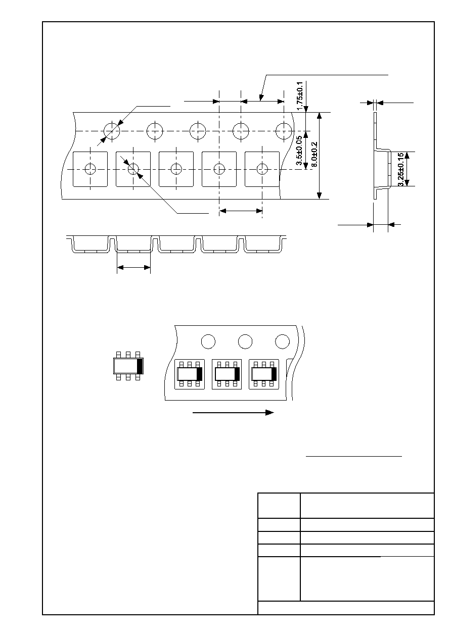
No. MP006-A-C-SD-3.1
MP006-A-C-SD-3.1
SOT236-A-Carrier Tape
Feed direction
4.0±0.1(10 pitches:40.0±0.2)
No.
TITLE
SCALE
UNIT
mm
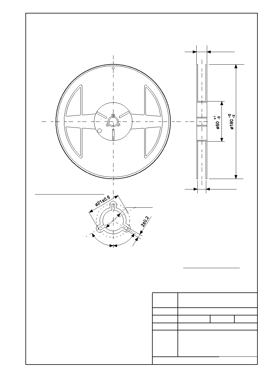
12.5max.
9.0±0.3
ø13±0.2
(60°)
(60°)
QTY
3,000
Seiko Instruments Inc.
Enlarged drawing in the central part
No. MP006-A-R-SD-2.1
MP006-A-R-SD-2.1
SOT236-A-Reel
1.8±0.15
0.5±0.1
0.5±0.1
0.8±0.05
0.14±0.05
R(0.075)
0.2±0.08
(0.125)
1
2
3
4
5
6
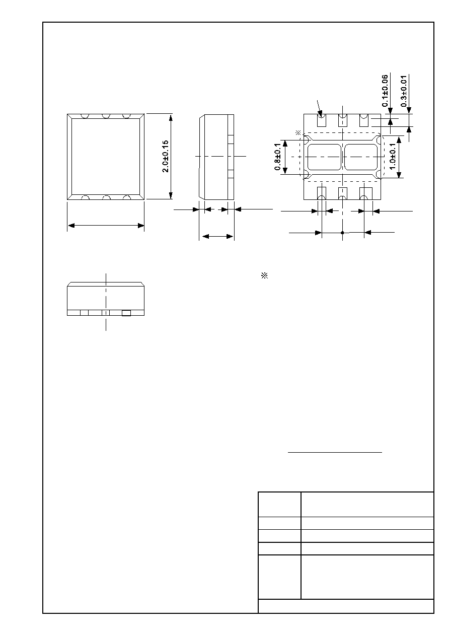
SNB6B-A-PKG Dimensions
No. BD006-A-P-SD-3.0
Seiko Instruments Inc.
No.
TITLE
SCALE
UNIT
mm
BD006-A-P-SD-3.0
The heatsink of back side has different electric
potential depending on the product.
Confirm specifications of each product.
Do not use it as the function of electrode.
0.2±0.08
No.
TITLE
SCALE
UNIT
mm
4.0±0.1
2.0±0.05
4.0±0.1
ø1.5±0.1
2.2±0.1
1.1±0.1
0.25±0.05
ø1.1±0.1
Seiko Instruments Inc.
Feed direction
SNB6B-A-Carrier Tape
No. BD006-A-C-SD-2.1
BD006-A-C-SD-2.1
1
2
3
6
5
4
QTY.
3,000
No.
TITLE
SCALE
UNIT
mm
12.5max.
9.0±0.3
ø13±0.2
Seiko Instruments Inc.
Enlarged drawing in the central part
SNB6B-A-Reel
No. BD006-A-R-SD-1.1
BD006-A-R-SD-1.1

·
The information described herein is subject to change without notice.
·
Seiko Instruments Inc. is not responsible for any problems caused by circuits or diagrams described herein
whose related industrial properties, patents, or other rights belong to third parties. The application circuit
examples explain typical applications of the products, and do not guarantee the success of any specific
mass-production design.
·
When the products described herein are regulated products subject to the Wassenaar Arrangement or other
agreements, they may not be exported without authorization from the appropriate governmental authority.
·
Use of the information described herein for other purposes and/or reproduction or copying without the
express permission of Seiko Instruments Inc. is strictly prohibited.
·
The products described herein cannot be used as part of any device or equipment affecting the human
body, such as exercise equipment, medical equipment, security systems, gas equipment, or any apparatus
installed in airplanes and other vehicles, without prior written permission of Seiko Instruments Inc.
·
Although Seiko Instruments Inc. exerts the greatest possible effort to ensure high quality and reliability, the
failure or malfunction of semiconductor products may occur. The user of these products should therefore
give thorough consideration to safety design, including redundancy, fire-prevention measures, and
malfunction prevention, to prevent any accidents, fires, or community damage that may ensue.
Document Outline
- S-8261 Series
- Cover
- Features
- Applications
- Packages
- Block Diagrams
- Product Name Structure
- Pin Configurations
- Absolute Maximum Ratings
- Electrical Characteristics
- Test Circuits
- Operation
- Operation Timing Chart
- Battery Protection IC Connection Example
- Precautions
- Characteristics (Typical Data)
- Package Drawings