/home/web/doc/html/sii/215972

Contents
Features.............................................................
1
Applications........................................................
1
Block Diagram ...................................................
1
Selection Guide..................................................
2
Pin Assignment..................................................
2
Absolute Maximum Ratings ...............................
2
Electrical Characteristics ...................................
3
Measurement Circuits........................................
7
Operation ...........................................................
8
Recommended Selection of Series Products
and External Parts .................... 12
Standard Circuits ............................................... 15
Design Precautions............................................ 16
Application Circuits ............................................ 17
Dimensions ........................................................ 19
Marking .............................................................. 19
Taping ................................................................ 20
Temperature Characteristics ............................. 21
Power Supply Dependency Characteristics....... 21
Transitory Response Characteristics................. 23
Reference Data.................................................. 26
Frequently Asked Questions.............................. 31
Rev.2.8
Seiko Instruments Inc.
1
STEP-UP SWITCHING REGULATOR
FOR LCD BIAS SUPPLY
S-8330/8331 Series
The S-8330/8331 Series is a CMOS PWM-control step-up switching
regulator which mainly consists of a reference voltage source, an
oscillation circuit, a power MOS FET (for S-8330 Series) , and an error
amplifier. The output voltage can adjust by built-in Electric volume circuit
, and equip with shutdown function. The S-8330 Series is low current
consumption because of CMOS structure , and a step-up switching
regulator constructed by externally connecting only a coil, a capacitor
and a diode. This feature, along with its 8-Pin SSOP package and a few
external components, makes the S-8330 Series ideal for LCD bias
generators of portable equipment. For applications requiring a high
output current, products used with an external transistor (S-8331 Series)
are also available.
Features
Applications
Maximum output voltage: 20 V to 30 V (2 V step)
Power supplies for medium type or large type
12 V range can be adjusted by electric volume
LCD panel.
Output current: 5mA ( V
IN
= 5 V,V
OUT
= 30 V)
Power supplies for portable devices such as
Low current consumption :
pagers, handy calculators, and remote controllers
During operation: 100
A (typ.) (V
IN
= 5 V 180 kHz)
Constant voltage power supplies for cameras,
During shutdown : 1.0
A (max.)
video equipment, and communications equipment
Shutdown function: Stepping up operation is stopped ,
and Vout pin is shorted to GND while shutdown.
Input voltage range: 2.0 to 9.0 V
Soft start function: 3 msec (typ.)
Built-in CR oscillation circuit:
Oscillating frequency: 180 kHz (typ.) (A series)
Oscillating frequency: 50 kHz (typ.) (B series)
8-pin SSOP plastic package
8-bit built-in electric volume circuit
External transistor type is available (S-8331 Series)
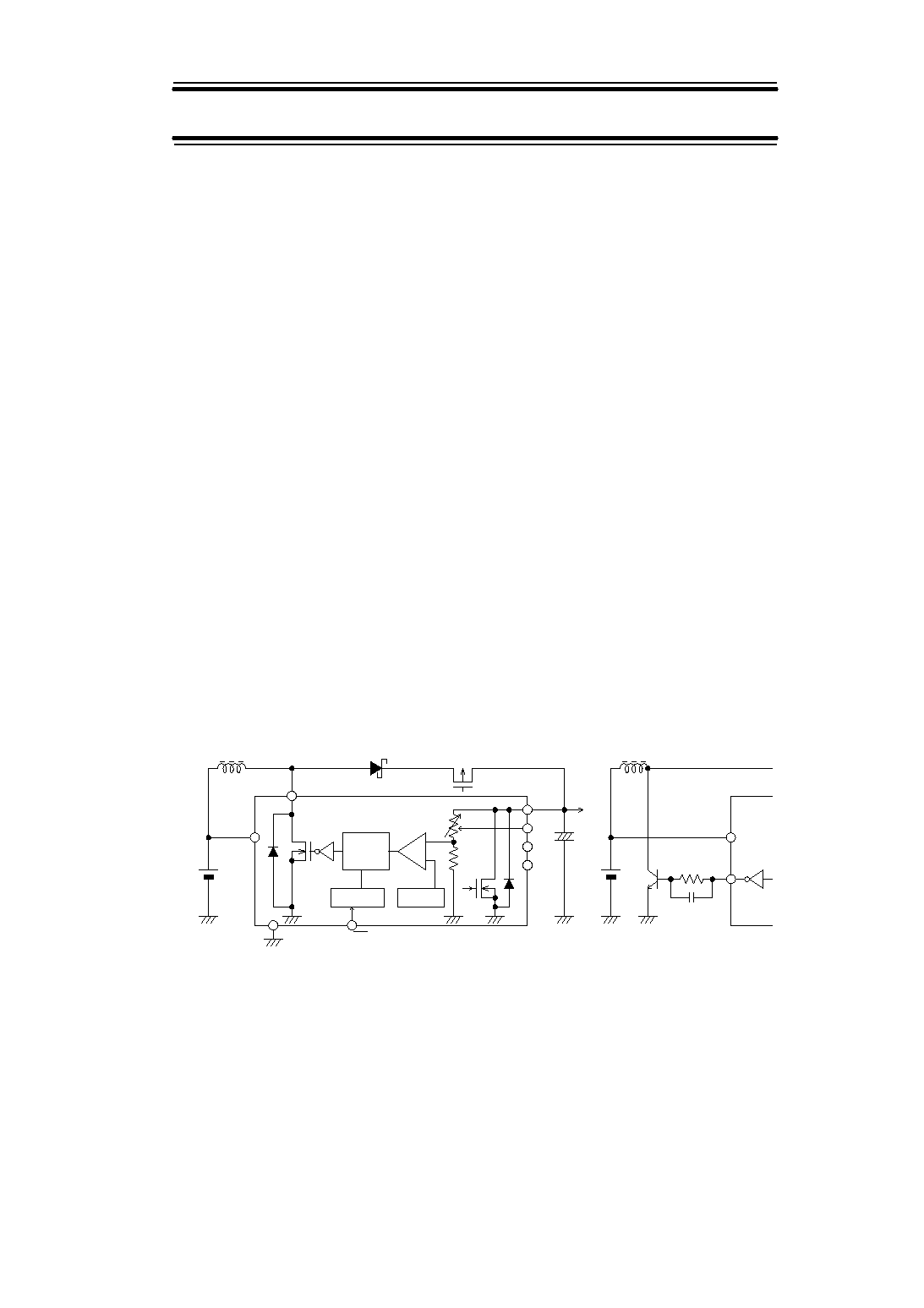
Block Diagram
(1) S-8330 Series
(2)
S-8331 Series
Figure 1 Block Diagram
CONT
RESET
ON/OFF
SD
V
OUT
V
SS
CR Oscillation
Circuit
V
REF
PWM
Control
Circuit
+
-
V
IN
V
IN
L
-
+
External
Transistor
Rb
Cb
VDIN
VCLK
VSTRB
CL
EXT
L
STEP-UP SWITCHING REGULATOR FOR LCD BIAS SUPPLY
S-8330/8331 Series Rev.2.8
2
Seiko Instruments Inc.
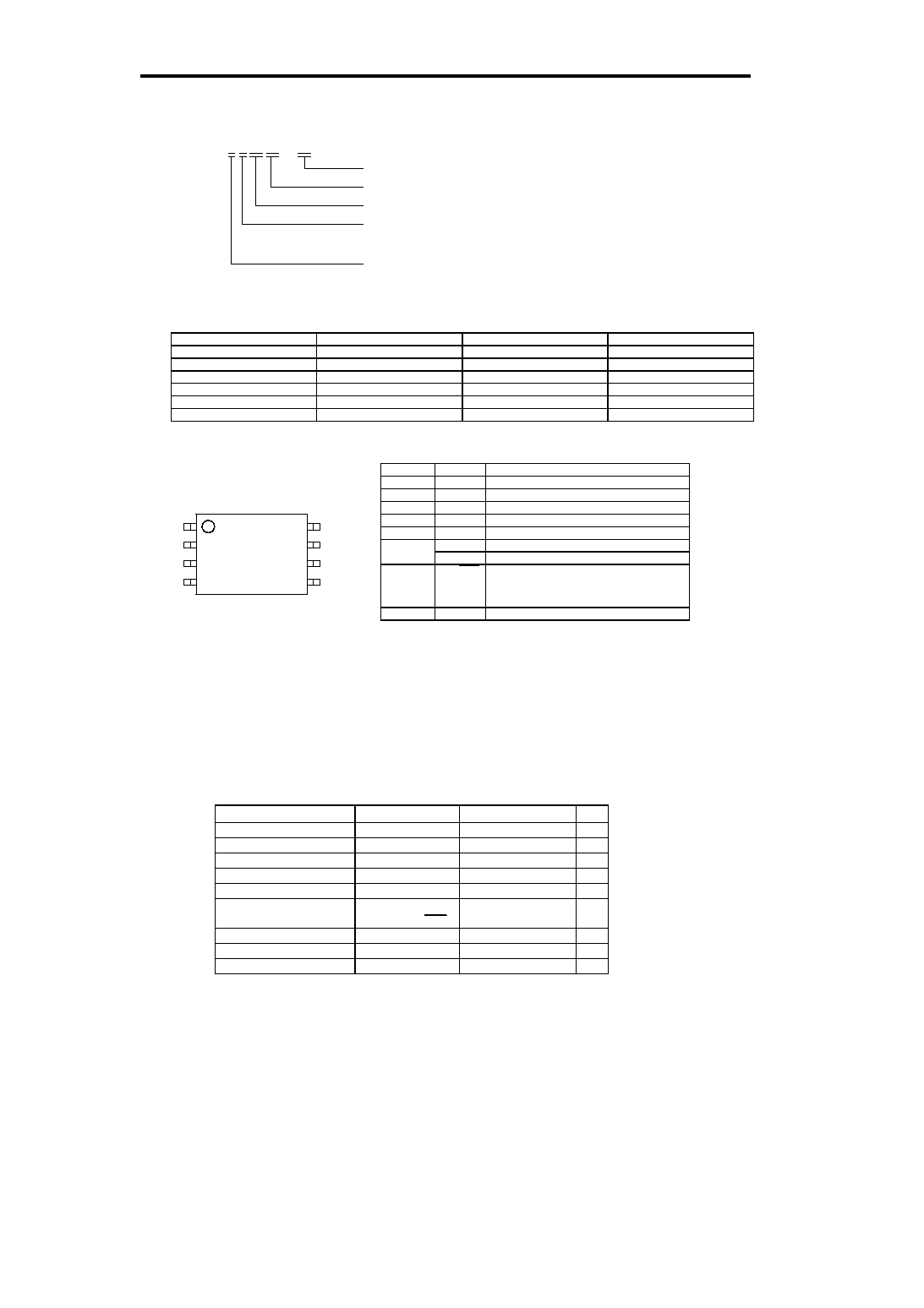
Selection Guide
1. Product Name
S
-
833 X X XX FS
-
T2
Tape Specification
Package name (abbreviation)
Maximum Output voltage
Product category
A: fosc=180kHz
B: fosc= 50kHz
Power transistor
0: Built-in switch.
1: External transistor.
2. Product list
Output voltage range (V)
S-8330AXXFS
Series
S-8330BXXFS
Series
S-8331AXXFS
Series
8 to 20
S-8330A20FS-T2
S-8330B20FS-T2
S-8331A20FS-T2
10 to 22
S-8330A22FS-T2
S-8330B22FS-T2
S-8331A22FS-T2
12 to 24
S-8330A24FS-T2
S-8330B24FS-T2
S-8331A24FS-T2
14 to 26
S-8330A26FS-T2
S-8330B26FS-T2
S-8331A26FS-T2
16 to 28
S-8330A28FS-T2
S-8330B28FS-T2
S-8331A28FS-T2
18 to 30
S-8330A30FS-T2
S-8330B30FS-T2
S-8331A30FS-T2
Pin Assignment
8-pin SSOP
Top view
8
7
6
5
4
1
3
2
Figure 2 Pin Assignment
Absolute Maximum Ratings
Note:
Built-in protect circuit for static electricity on chip.
However, prevent a charge of static electricity which exceeds the capacity of the protection circuit.
(Unless otherwise specified: Ta=25
�
C)
Parameter
Symbol
Ratings
Unit
V
OUT
pin voltage
VOUT
V
SS
-0.3 to 33
V
CONT pin voltage
VCONT
V
SS
-0.3 to 33
V
CONT pin current
ICONT
300
mA
EXT pin voltage
VEXT
V
SS
-0.3 to VOUT+0.3
V
EXT pin current
IEXT
�50
mA
Input voltage
VIN,VCLK,VDIN,
VSTRB,ON/OFF
V
SS
-0.3 to 10
V
Power dissipation
PD
300
mW
Operating temperature range
TOPR
-20 to +70
�
C
Storage temperature range
TSTG
-40 to +125
�
C
Pin No.
Pin name
Functions
1
VDIN
Electric volume data input pin
2
VCLK
Electric volume clock input pin
3
VSTRB Electric volume strobe signal input pin
4
V
OUT
Output voltage pin
5
V
IN
Power supply pin
6
CONT
External inductor connection pin (Note 1)
EXT
External transistor connection pin (Note 2 )
7
ON/OFF
Shutdown pin
"H":normal operation
(stepping up operation)
"L":stop stepping up operation
8
V
SS
GND pin
Note 1: S-8330 Series: Open drain output
Note 2: S-8331 Series: CMOS output
STEP-UP SWITCHING REGULATOR FOR LCD BIAS SUPPLY
Rev.2.8
S-8330/8331 Series
Seiko Instruments Inc.
3
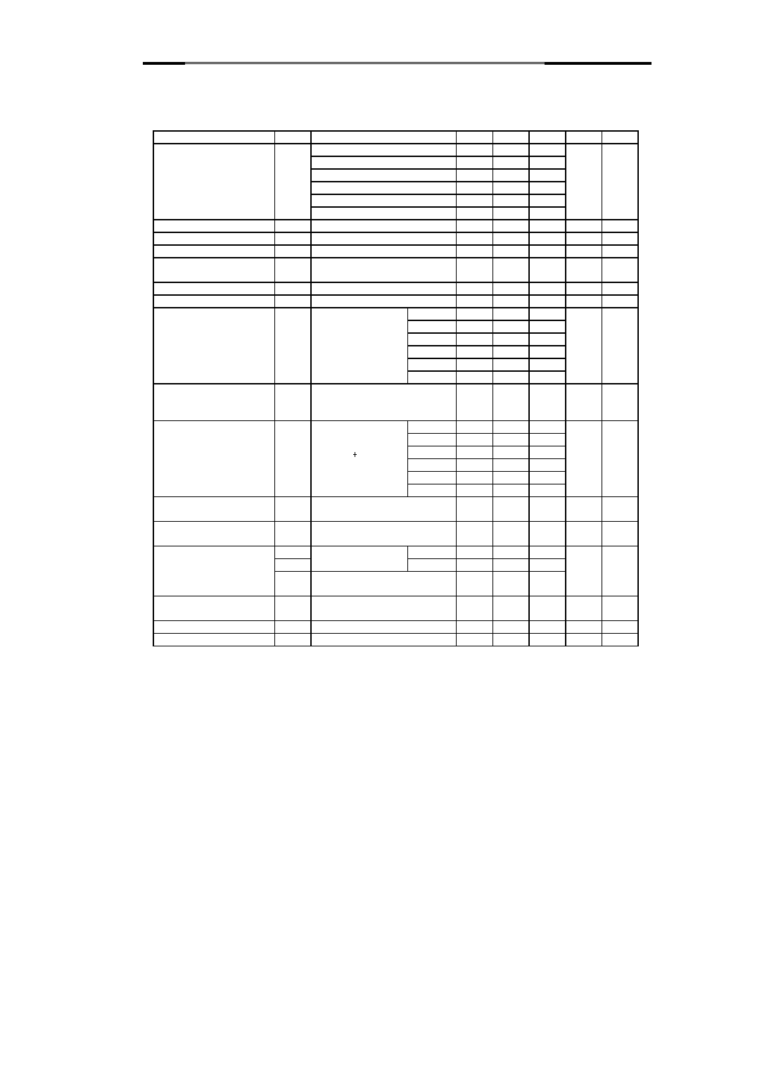
Electrical Characteristics
1. S-8330A Series
Step-Up Switching Regulator
(Unless otherwise specified: Ta=25
C)
Items
Symbols
Conditions
Min.
Typ.
Max.
Unit
Mea.Circ.
S-8330A20FS
8
--
20
S-8330A22FS
10
--
22
Output voltage range
VOUT
S-8330A24FS
12
--
24
V
5
S-8330A26FS
14
--
26
S-8330A28FS
16
--
28
S-8330A30FS
18
--
30
Input voltage
VIN
2.0
--
9.0
V
2
Current consumption 1
ISS1
V
IN
=5V, V
OUT
= Output voltage Max.
--
100
200
A
4
Current consumption 2
ISS2
V
IN
=2V, V
OUT
= Output voltage Min.
--
50
100
A
4
Current consumption during power off
ISSS
Power off pin
=VDATA=0V,V
IN
=VCLK=VSTRB=5V
--
--
1.0
A
4
Switching current
ISW
VCONT=0.4V
100
200
--
mA
--
Switching transistor leakage current
ISWQ
Power off pin =0V , VCONT=9V
--
--
1.0
A
3
S-8330A20FS
--
�300
--
S-8330A22FS
--
�330
--
Line regulation
VOUT1 V
IN
=3V to 6V
S-8330A24FS
--
�360
--
mV
5
S-8330A26FS
--
�390
--
S-8330A28FS
--
�420
--
S-8330A30FS
--
�450
--
Load regulation
VOUT2 V
IN
=5V
I
OUT
=output voltage/2.4M
to
output voltage/24k
--
�30
--
mV
5
S-8330A20FS
--
�1.0
--
S-8330A22FS
--
�1.1
--
Output voltage temperature coefficient
VOUT
Ta= -20
C to 70
C
S-8330A24FS
--
�1.2
--
mV
5
/
Ta
S-8330A26FS
--
�1.3
--
/
C
S-8330A28FS
--
�1.4
--
S-8330A30FS
--
�1.5
--
Oscillating frequency
fosc
V
OUT
=output voltage
0.95
Measure waveform at CONT pin
144
180
216
kHz
2
Maximum duty ratio
Max Duty V
OUT
=output voltage
0.95
Measure waveform at CONT pin
60
72
84
2
VSH1
V
OUT
=output voltage
0.95
V
IN
3.0V
2.4
--
--
Power off terminal
VSH2
Check oscillation at CONT pin V
IN
3.0V
1.6
--
--
V
2
input voltage
VSL
V
OUT
=output voltage
0.95
Check oscillation stop at CONT pin
--
--
0.4
Power off terminal
input leakage current
ISL
V
IN
=9V
-1
--
1
A
1
Soft start time
TSS
1
3
6
ms
--
Efficiency
EFFI
--
85
--
5
Externally attached parts:
Coils
CD54 (47
H) of Sumida Electric Co., Ltd.
Diodes
MA720 Schottky type of Matsushita Electronic Components Co., Ltd.
Capacitors
F93 tantalum type (two circuits of 50V, 4.7
F are connected in parallel) of Nichicon Corporation
V
IN
=5V, V
OUT
=VOUT Max. I
OUT
= output voltage /24k
ON/OFF=5V,VDATA=VCLK=VSTRB=0V
Note: Output voltage specified above is the typical value of the output voltage.
STEP-UP SWITCHING REGULATOR FOR LCD BIAS SUPPLY
S-8330/8331 Series Rev.2.8
4
Seiko Instruments Inc.
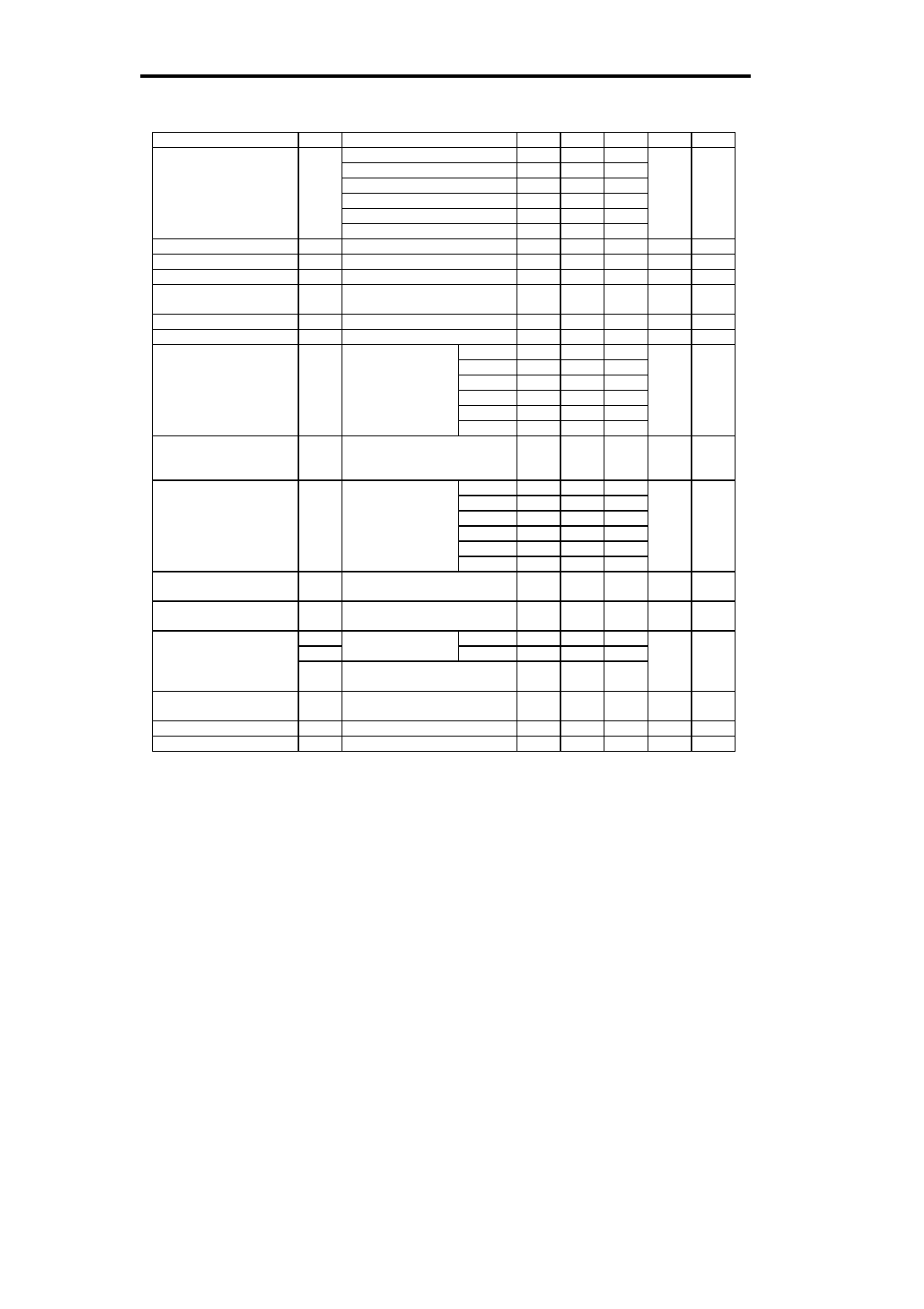
2. S-8330B Series
Step-Up Switching Regulator
(Unless otherwise specified: Ta=25
C)
Item
Symbol
Conditions
Min.
Typ.
Max.
Unit
Mea. Cir.
S-8330B20FS
8
--
20
S-8330B22FS
10
--
22
Output voltage range
VOUT
S-8330B24FS
12
--
24
V
5
S-8330B26FS
14
--
26
S-8330B28FS
16
--
28
S-8330B30FS
18
--
30
Input voltage
VIN
2.0
--
9.0
V
2
Current consumption 1
ISS1
V
IN
=5V, V
OUT
=Output voltage Max.
--
40
80
A
4
Current consumption 2
ISS2
V
IN
=2V, V
OUT
=Output voltage Min.
--
20
40
A
4
Current consumption during power off
ISSS
Power off pin
=VDATA=0V,V
IN
=VCLK=VSTRB=5V
--
--
1.0
A
4
Switching current
ISW
VCONT=0.4V
100
200
--
mA
--
Switching transistor leakage current
ISWQ
Power off pin=0V , VCONT=9V
--
--
1.0
A
3
S-8330B20FS
--
�300
--
S-8330B22FS
--
�330
--
Line regulation
VOUT1 V
IN
=3V to 6V
S-8330B24FS
--
�360
--
mV
5
S-8330B26FS
--
�390
--
S-8330B28FS
--
�420
--
S-8330B30FS
--
�450
--
Load regulation
VOUT2 V
IN
=5V
I
OUT
=Output voltage/2.4M
to
Output voltage/24k
--
�30
--
mV
5
S-8330B20FS
--
�1.0
--
S-8330B22FS
--
�1.1
--
Output voltage Temperature coefficient
VOUT
Ta=-20
C to +70
C
S-8330B24FS
--
�1.2
--
mV
5
/
Ta
S-8330B26FS
--
�1.3
--
/
C
S-8330B28FS
--
�1.4
--
S-8330B30FS
--
�1.5
--
Oscillating frequency
fosc
V
OUT
=Output voltage
0.95
Measure waveform at CONT pin
40
50
60
kHz
2
Maximum duty ratio
Max Duty V
OUT
=Output voltage
0.95
Measure waveform at CONT pin
60
72
84
%
2
VSH1
V
OUT
=Output voltage
0.95
V
IN
3.0V
2.4
--
--
Power off pin
VSH2
Check oscillation at CONT pin V
IN
3.0V
1.6
--
--
V
2
Input voltage
VSL
V
OUT
=Output voltage
0.95
Check oscillation stop at CONT pin
--
--
0.4
Power off pin
Input leakage current
ISL
V
IN
=9V
-1
--
1
A
1
Soft start time
TSS
3
10
20
ms
--
Efficiency
EFFI
--
85
--
%
5
Externally attached parts:
Coils
CD54 (47
H) of Sumida Electric Co., Ltd.
Diodes
MA720 Schottky type of Matsushita Electronic Components Co., Ltd.
Capacitors
F93 tantalum type (two circuits of 50V, 4.7
F are connected in parallel) of Nichicon Corporation
V
IN
=5V,V
OUT
=VOUT Max. I
OUT
= output voltage /24k
ON/OFF=5V,VDATA=VCLK=VSTRB=0V
Note: Output voltage specified above is the typical value of the output voltage.