 | –≠–ª–µ–∫—Ç—Ä–æ–Ω–Ω—ã–π –∫–æ–º–ø–æ–Ω–µ–Ω—Ç: S-8330A20 | –°–∫–∞—á–∞—Ç—å:  PDF PDF  ZIP ZIP |
Document Outline
- ˛ˇ
- ˛ˇ
- ˛ˇ
- ˛ˇ
- ˛ˇ
- ˛ˇ
- ˛ˇ
- ˛ˇ
- ˛ˇ
- ˛ˇ
- ˛ˇ
- ˛ˇ
- ˛ˇ
- ˛ˇ
- ˛ˇ
- ˛ˇ
- ˛ˇ
- ˛ˇ
- ˛ˇ
- ˛ˇ
- ˛ˇ
- ˛ˇ

Rev.4.1
Seiko Instruments Inc.
1
STEP-UP SWITCHING REGULATOR
FOR LCD BIAS SUPPLY
S-8330/8331 Series
The S-8330/8331 Series is a CMOS PWM-control step-up switching
regulator which mainly consists of a reference voltage source, an
oscillation circuit, a power MOS FET (for S-8330 Series) , and an error
amplifier. The output voltage can adjust by built-in Electric volume circuit
, and equip with shutdown function. The S-8330 Series is low current
consumption because of CMOS structure , and a step-up switching
regulator constructed by externally connecting only a coil, a capacitor
and a diode. This feature, along with its 8-Pin SSOP package and a few
external components, makes the S-8330 Series ideal for LCD bias
generators of portable equipment. For applications requiring a high
output current, products used with an external transistor (S-8331 Series)
are also available.
T
Features
T
Applications
∑
Maximum output voltage: 20 V to 30 V (2 V step)
∑
Power supplies for medium type or large type
12 V range can be adjusted by electric volume
LCD panel.
∑
Output voltage accuracy :
±
2.4%
∑
Power supplies for portable devices such as
∑
Output current: 5mA ( V
IN
= 5 V,V
OUT
= 30 V)
pagers, handy calculators, and remote controllers
∑
Low current consumption :
∑
Constant voltage power supplies for cameras,
During operation: 100
µ
A (typ.) (V
IN
= 5 V 180 kHz)
video equipment, and communications equipment
During shutdown : 1.0
µ
A (max.)
∑
Shutdown function: Stepping up operation is stopped ,
and Vout pin is shorted to GND while shutdown.
∑
Input voltage range: 2.0 to 9.0 V
∑
Soft start function: 3 msec (typ.)
∑
Built-in CR oscillation circuit:
Oscillating frequency: 180 kHz (typ.) (A series)
Oscillating frequency: 50 kHz (typ.) (B series)
∑
8-pin SSOP plastic package
∑
8-bit built-in electric volume circuit
∑
External transistor type is available (S-8331 Series)
T
Package
8-pin SSOP plastic package (PKG drawing code : FS008-A)

STEP-UP SWITCHING REGULATOR FOR LCD BIAS SUPPLY
S-8330/8331 Series Rev.4.1
2
Seiko Instruments Inc.
T
Block Diagram
CONT
RESET
ON/OFF
SD
V
OUT
V
SS
CR Oscillation
Circuit
V
REF
PWM
Control
Circuit
+
-
V
IN
V
IN
L
-
+
External
Transistor
Rb
Cb
VDIN
VCLK
VSTRB
CL
EXT
L
(1) S-8330 Series
(2)
S-8331 Series
Figure 1 Block Diagram
T
Selection Guide
1. Product Name
S
833 X X XX FS
T2
Tape Specification
Package name (abbreviation)
Maximum Output voltage
Product category
A: fosc=180kHz
B: fosc= 50kHz
Power transistor
0: Built-in switch.
1: External transistor.
2.
Product list
Output voltage range (V)
S-8330AXXFS
Series
S-8330BXXFS
Series
S-8331AXXFS
Series
8 to 20
S-8330A20FS-T2
S-8330B20FS-T2
S-8331A20FS-T2
10 to 22
S-8330A22FS-T2
S-8330B22FS-T2
S-8331A22FS-T2
12 to 24
S-8330A24FS-T2
S-8330B24FS-T2
S-8331A24FS-T2
14 to 26
S-8330A26FS-T2
S-8330B26FS-T2
S-8331A26FS-T2
16 to 28
S-8330A28FS-T2
S-8330B28FS-T2
S-8331A28FS-T2
18 to 30
S-8330A30FS-T2
S-8330B30FS-T2
S-8331A30FS-T2
STEP-UP SWITCHING REGULATOR FOR LCD BIAS SUPPLY
Rev.4.1 S-8330/8331 Series
Seiko Instruments Inc.
3
T
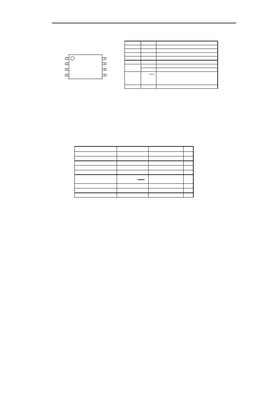
Pin Assignment
8-pin SSOP
Top view
8
7
6
5
4
1
3
2
Figure 2 Pin Assignment
T
Absolute Maximum Ratings
Note:
Built-in protect circuit for static electricity on chip.
However, prevent a charge of static electricity which exceeds the capacity of the protection circuit.
(Unless otherwise specified: Ta=25
∞
C)
Parameter
Symbol
Ratings
Unit
V
OUT
pin voltage
VOUT
V
SS
-0.3 to 33
V
CONT pin voltage
VCONT
V
SS
-0.3 to 33
V
CONT pin current
ICONT
300
mA
EXT pin voltage
VEXT
V
SS
-0.3 to VOUT+0.3
V
EXT pin current
IEXT
±50
mA
Input voltage
VIN,VCLK,VDIN,
VSTRB,ON/OFF
V
SS
-0.3 to 10
V
Power dissipation
PD
300
mW
Operating temperature range
TOPR
-20 to +70
∞
C
Storage temperature range
TSTG
-40 to +125
∞
C
Pin No.
Pin name
Functions
1
VDIN
Electric volume data input pin
2
VCLK
Electric volume clock input pin
3
VSTRB Electric volume strobe signal input pin
4
V
OUT
Output voltage pin
5
V
IN
Power supply pin
6
CONT
External inductor connection pin (Note 1)
EXT
External transistor connection pin (Note 2 )
7
ON/OFF
Shutdown pin
"H":normal operation
(stepping up operation)
"L":stop stepping up operation
8
V
SS
GND pin
Note 1: S-8330 Series: Open drain output
Note 2: S-8331 Series: CMOS output
STEP-UP SWITCHING REGULATOR FOR LCD BIAS SUPPLY
S-8330/8331 Series Rev.4.1
4
Seiko Instruments Inc.
T
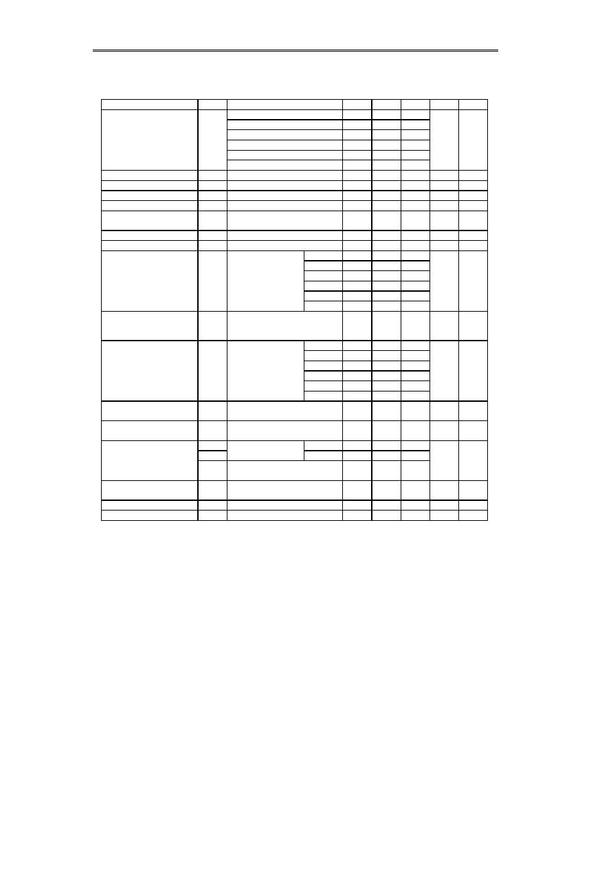
Electrical Characteristics
1. S-8330A Series
Step-Up Switching Regulator
(Unless otherwise specified: Ta=25
∞
C)
Items
Symbols
Conditions
Min.
Typ.
Max.
Unit
Mea.Circ.
S-8330A20FS
8
--
20
S-8330A22FS
10
--
22
Output voltage range
VOUT
S-8330A24FS
12
--
24
V
5
S-8330A26FS
14
--
26
S-8330A28FS
16
--
28
S-8330A30FS
18
--
30
Output voltage accuracy
±
2.4%
%
5
Input voltage
VIN
2.0
--
9.0
V
2
Current consumption 1
ISS1
V
IN
=5V, V
OUT
= Output voltage Max.
--
100
200
µ
A
4
Current consumption 2
ISS2
V
IN
=2V, V
OUT
= Output voltage Min.
--
50
100
µ
A
4
Current consumption during power off
ISSS
Power off pin
=VDIN=0V,V
IN
=VCLK=VSTRB=5V
--
--
1.0
µ
A
4
Switching current
ISW
VCONT=0.4V
100
200
--
mA
--
Switching transistor leakage current
ISWQ
Power off pin =0V , VCONT=9V
--
--
1.0
µ
A
3
S-8330A20FS
--
±300
--
S-8330A22FS
--
±330
--
Line regulation
VOUT1 V
IN
=3V to 6V
S-8330A24FS
--
±360
--
mV
5
S-8330A26FS
--
±390
--
S-8330A28FS
--
±420
--
S-8330A30FS
--
±450
--
Load regulation
VOUT2 V
IN
=5V
I
OUT
=output voltage/2.4M
to
output voltage/24k
--
±30
--
mV
5
S-8330A20FS
--
±1.0
--
S-8330A22FS
--
±1.1
--
Output voltage temperature coefficient
VOUT
Ta= -20
∞
C to
70
∞
C
S-8330A24FS
--
±1.2
--
mV
5
/
Ta
S-8330A26FS
--
±1.3
--
/
∞
C
S-8330A28FS
--
±1.4
--
S-8330A30FS
--
±1.5
--
Oscillating frequency
fosc
V
OUT
=output voltage
◊
0.95
Measure waveform at CONT pin
144
180
216
kHz
2
Maximum duty ratio
Max Duty V
OUT
=output voltage
◊
0.95
Measure waveform at CONT pin
60
72
84
%
2
VSH1
V
OUT
=output voltage
◊
0.95
V
IN
3.0V
2.4
--
--
Power off terminal
VSH2
Check oscillation at CONT pin V
IN
<
3.0V
1.6
--
--
V
2
input voltage
VSL
V
OUT
=output voltage
◊
0.95
Check oscillation stop at CONT pin
--
--
0.4
Power off terminal
input leakage current
ISL
V
IN
=9V
-1
--
1
µ
A
1
Soft start time
TSS
1
3
6
ms
--
Efficiency
EFFI
--
85
--
%
5
Externally attached parts:
Coils
:
CD54 (47
µ
H) of Sumida Electric Co., Ltd.
Diodes
:
MA720 Schottky type of Matsushita Electronic Components Co., Ltd.
Capacitors
:
F93 tantalum type (two circuits of 50V, 4.7
µ
F are connected in parallel) of Nichicon Corporation
V
IN
=5V, V
OUT
=VOUT Max. I
OUT
= output voltage /24k
ON/OFF=5V,VDIN=VCLK=VSTRB=0V
Note: Output voltage specified above is the typical value of the output voltage.
STEP-UP SWITCHING REGULATOR FOR LCD BIAS SUPPLY
Rev.4.1 S-8330/8331 Series
Seiko Instruments Inc.
5
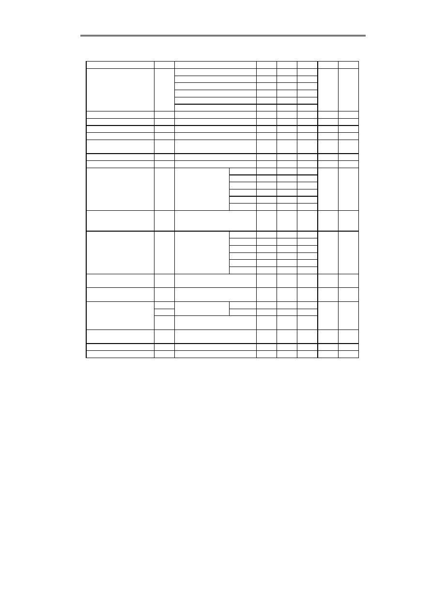
2. S-8330B Series
Step-Up Switching Regulator
(Unless otherwise specified: Ta=25
∞
C)
Item
Symbol
Conditions
Min.
Typ.
Max.
Unit
Mea. Cir.
S-8330B20FS
8
--
20
S-8330B22FS
10
--
22
Output voltage range
VOUT
S-8330B24FS
12
--
24
V
5
S-8330B26FS
14
--
26
S-8330B28FS
16
--
28
S-8330B30FS
18
--
30
Output voltage accuracy
±
2.4%
%
5
Input voltage
VIN
2.0
--
9.0
V
2
Current consumption 1
ISS1
V
IN
=5V, V
OUT
=Output voltage Max.
--
40
80
µ
A
4
Current consumption 2
ISS2
V
IN
=2V, V
OUT
=Output voltage Min.
--
20
40
µ
A
4
Current consumption during power off
ISSS
Power off pin
=VDIN=0V,V
IN
=VCLK=VSTRB=5V
--
--
1.0
µ
A
4
Switching current
ISW
VCONT=0.4V
100
200
--
mA
--
Switching transistor leakage current
ISWQ
Power off pin=0V , VCONT=9V
--
--
1.0
µ
A
3
S-8330B20FS
--
±300
--
S-8330B22FS
--
±330
--
Line regulation
VOUT1 V
IN
=3V to 6V
S-8330B24FS
--
±360
--
mV
5
S-8330B26FS
--
±390
--
S-8330B28FS
--
±420
--
S-8330B30FS
--
±450
--
Load regulation
VOUT2 V
IN
=5V
I
OUT
=Output voltage/2.4M
to
Output voltage/24k
--
±30
--
mV
5
S-8330B20FS
--
±1.0
--
S-8330B22FS
--
±1.1
--
Output voltage Temperature coefficient
VOUT
Ta=-20
∞
C to +70
∞
C
S-8330B24FS
--
±1.2
--
mV
5
/
Ta
S-8330B26FS
--
±1.3
--
/
∞
C
S-8330B28FS
--
±1.4
--
S-8330B30FS
--
±1.5
--
Oscillating frequency
fosc
V
OUT
=Output voltage
◊
0.95
Measure waveform at CONT pin
40
50
60
kHz
2
Maximum duty ratio
Max Duty V
OUT
=Output voltage
◊
0.95
Measure waveform at CONT pin
60
72
84
%
2
VSH1
V
OUT
=Output voltage
◊
0.95
V
IN
3.0V
2.4
--
--
Power off pin
VSH2
Check oscillation at CONT pin V
IN
<
3.0V
1.6
--
--
V
2
Input voltage
VSL
V
OUT
=Output voltage
◊
0.95
Check oscillation stop at CONT pin
--
--
0.4
Power off pin
Input leakage current
ISL
V
IN
=9V
-1
--
1
µ
A
1
Soft start time
TSS
3
10
20
ms
--
Efficiency
EFFI
--
85
--
%
5
Externally attached parts:
Coils
:
CD54 (47
µ
H) of Sumida Electric Co., Ltd.
Diodes
:
MA720 Schottky type of Matsushita Electronic Components Co., Ltd.
Capacitors
:
F93 tantalum type (two circuits of 50V, 4.7
µ
F are connected in parallel) of Nichicon Corporation
V
IN
=5V,V
OUT
=VOUT Max. I
OUT
= output voltage /24k
ON/OFF=5V,VDIN=VCLK=VSTRB=0V
Note: Output voltage specified above is the typical value of the output voltage.

STEP-UP SWITCHING REGULATOR FOR LCD BIAS SUPPLY
S-8330/8331 Series Rev.4.1
6
Seiko Instruments Inc.
3. S-8331A Series
Step-Up Switching Regulator
(Unless otherwise specified: Ta=25
∞
C)
Item
Symbol
Conditions
Min.
Typ.
Max.
Unit
Mea. Cir.
S-8330A20FS
8
--
20
S-8330A22FS
10
--
22
Output voltage range
VOUT
S-8330A24FS
12
--
24
V
6
S-8330A26FS
14
--
26
S-8330A28FS
16
--
28
S-8330A30FS
18
--
30
Output voltage accuracy
±
2.4%
%
5
Input voltage
VIN
2.0
--
9.0
V
2
Current consumption 1
ISS1
V
IN
=5V, V
OUT
=Output voltage Max.
--
50
100
µ
A
4
Current consumption 2
ISS2
V
IN
=2V, V
OUT
=Output voltage Min.
--
25
50
µ
A
4
Current consumption during power off
ISSS
Power off pin
=VDIN=0V,V
IN
=VCLK=VSTRB=5V
--
--
1.0
µ
A
4
Output current at EXTpin
IEXTH
VEXT=V
IN
-0.4V
3.0
5.0
--
mA
--
IEXTL
VEXT=0.4V
5.0
8.0
--
mA
--
S-8331A20FS
--
±300
--
S-8331A22FS
--
±330
--
Line regulation
VOUT1 V
IN
=3V to 6V
S-8331A24FS
--
±360
--
mV
6
S-8331A26FS
--
±390
--
S-8331A28FS
--
±420
--
S-8331A30FS
--
±450
--
Load regulation
VOUT2 V
IN
=5V
I
OUT
=Output voltage/2.4M
to
Output voltage/24k
--
±30
--
mV
6
S-8331A20FS
--
±1.0
--
S-8331A22FS
--
±1.1
--
Output voltage Temperature coefficient
VOUT
Ta=-20
∞
C to +70
∞
C
S-8331A24FS
--
±1.2
--
mV
6
/
Ta
S-8331A26FS
--
±1.3
--
/
∞
C
S-8331A28FS
--
±1.4
--
S-8331A30FS
--
±1.5
--
Oscillating frequency
fosc
V
OUT
=Output voltage
◊
0.95
Measure waveform at EXT pin
144
180
216
kHz
2
Maximum duty ratio
Max Duty V
OUT
=Output voltage
◊
0.95
Measure waveform at EXT pin
60
72
84
%
2
VSH1
V
OUT
=Output voltage
◊
0.95
V
IN
3.0V
2.4
--
--
Power off pin
VSH2
Check oscillation at EXT pin
V
IN
<
3.0V
1.6
--
--
V
2
Input voltage
VSL
V
OUT
=Output voltage
◊
0.95
Check oscillation stop at EXT pin
--
--
0.4
Power off pin
Input leakage current
ISL
V
IN
=9V
-1
--
1
µ
A
1
Soft start time
TSS
1
3
6
ms
--
Efficiency
EFFI
--
85
--
%
6
Externally attached parts:
Coils
:
CD54 (47
µ
H) of Sumida Electric Co., Ltd.
Diodes
:
MA720 Schottky type of Matsushita Electronic Components Co., Ltd.
Capacitors
:
F93 tantalum type (two circuits of 50V, 4.7
µ
F are connected in parallel) of Nichicon Corporation.
Transistors
:
2SD1624 of Sanyo Electric Inc.
Base resistance (Rb)
:
1.0k
Base capacitor (Cb)
:
2200pF (ceramic type)
V
IN
=5V, V
OUT
=VOUT Max. I
OUT
= output voltage/24k
ON/OFF=5V, VDIN=VCLK=VSTRB=0V
Note: Output voltage specified above is the typical value of the output voltage.
STEP-UP SWITCHING REGULATOR FOR LCD BIAS SUPPLY
Rev.4.1 S-8330/8331 Series
Seiko Instruments Inc.
7
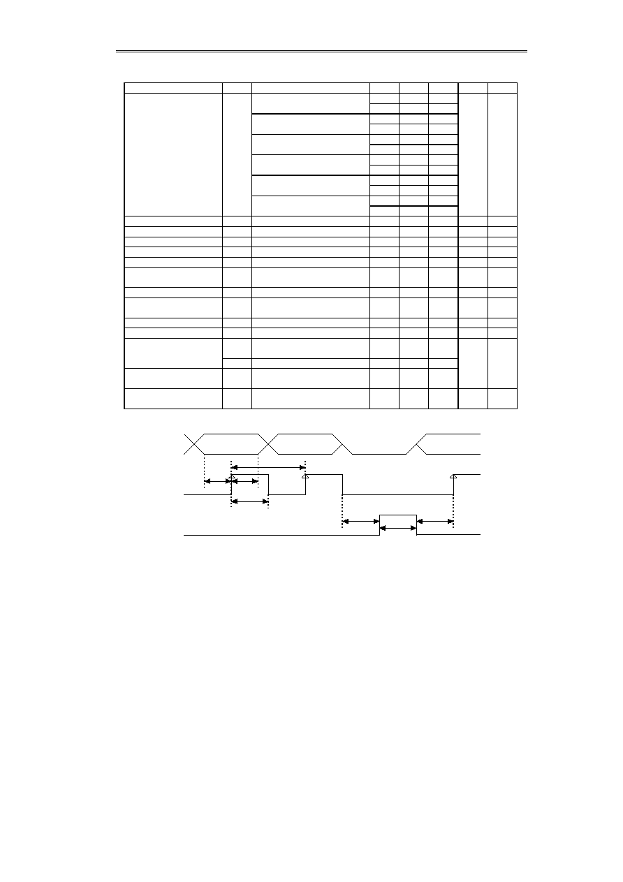
4. Characteristics Common to S-8330/31Series
Electric Volume
(Unless otherwise specified
:
Ta=25
∞
C)
Item
Symbol
Conditions
Min.
Typ.
Max.
Unit
Mea. cir.
S-833XX20FS
8
--
14
14
--
20
S-833XX22FS
10
--
16
16
--
22
S-833XX24FS
12
--
18
Output voltage range (Note 1)
VOUT
18
--
24
V
5 (6)
S-833XX26FS
14
--
20
20
--
26
S-833XX28FS
16
--
22
22
--
28
S-833XX30FS
18
--
24
24
--
30
Potential division accuracy
--
--
±2.4
%
5 (6)
Electric volume resolution
--
1/256
--
5 (6)
Error in linearity (Note 1)
--
--
±1/2
LSB
5 (6)
Data setup time
tsc
0.5
--
--
µ
s
--
Data hold time
thc
0.5
--
--
µ
s
--
VCLK falling edge to VSTRB rising
edge
tss
0.5
--
--
µ
s
--
VSTRB pulse width
tda
0.5
--
--
µ
s
--
VSTRB falling edge to VCLK rising
edge
ths
0.5
--
--
µ
s
--
VCLK pulse width
tdc
0.5
4.17
--
µ
s
--
VCLK period
ttc
5
8.33
--
µ
s
--
VDIN,VCLK,VSTRB Input voltage H
level
VSHC1
V
IN
3.0V
2.4
--
--
VSHC2
V
IN
<
3.0V
1.6
--
--
V
--
VDIN,VCLK,VSTRB Input voltage L
level
VSLC
--
--
0.2
VDIN,VCLK,VSTRB Input leakage
current
ISLC
V
IN
=9V
-1
--
1
µ
A
1
tss
ths
tda
ttc
tdc
thc
D1
next MSB
D2
VSTRB
VCLK
VDIN
tsc
Figure 3 Data Input Timing
Note 1: An electric volume has 8-bit resolution. However, its error in linearity may exceed ±1/2LSB only before and after switching from 127 to 128
(from 01111111 to 10000000) and vice versa. When the electric volume is used within the variable range of 12 V, its error in linearity
corresponds to 6 bits (±2.4% potential division accuracy is ensured).
STEP-UP SWITCHING REGULATOR FOR LCD BIAS SUPPLY
S-8330/8331 Series Rev.4.1
8
Seiko Instruments Inc.
T
Measurement Circuits
Meas
Pin
A
1
VIN
Other
Pins
Open
ON/OFF
VSS
A
$
VSS
*300
Not needed in the *S-8331 Series.
*5V
Oscilloscope
ON/OFF
CONT(EXT)
VIN
2
VDIN
VCLK
VSTRB
VOUT
VSS
ON/OFF
CONT
3
VIN
A
VDIN
VCLK
VSTRB
VOUT
VSS
ON/OFF
CONT(EXT)
VIN
4
A
VDIN
VCLK
VSTRB
VOUT
*300
Not needed in the *S-8331 Series.
*5V
A
VSS
ON/OFF
CONT
5
VIN
-
V
+
VDIN
VCLK
VSTRB
VOUT
-
+
VSS
ON/OFF
1k
2200pF
EXT
6
VIN
-
V
+
VDIN
VCLK
VSTRB
VOUT
-
+
Figure 4 Measurement Circuits
STEP-UP SWITCHING REGULATOR FOR LCD BIAS SUPPLY
Rev.4.1 S-8330/8331 Series
Seiko Instruments Inc.
9
T
Operation
1. Step-Up DC-DC Converter
The S-8330/31 Series is a DC-DC converter using a pulse width modulation method (PWM) with low current consumption.
Conventional PFM DC/DC converters have a drawback. Namely, an increase in the ripple voltage occurs because pulses
are skipped when low output load current flows and the ripple frequency of the output voltage varies. In the S-8330/31
Series, the pulse width varies in the range of 0 % to 72 % depending upon the load current, but the switching frequency does
not vary. This allows the ripple voltage due to switching to be reduced with a filter. Also, the internal soft start circuit controls
the rush current and the output voltage overshoot to be generated when the IC starts the step-up operation by setting the
power off pin to "H" level. At powering ON the IC, the rush current flows to charge up capacitive components of output
capacitor "C
OUT
" and load via coils and diodes.
ON/OFF
Electric
Volume
CONT
M1
OSC
Di
L
V
IN
V
OUT
C
OUT
-
-
+
+
Figure 5
Step-Up DC-DC Converter
The following are fundamental equations of step-up switching regulators [ (1) to (7) ] (see Figure 5).
The pin voltage at CONT immediatetly after M1 is turned ON (current I
L
which flows into L is zero):
Change in I
L
with time:
Integreation of the above equation (I
L
) is as follows:
I
L
flows into L during t
ON
. The time is determined depending upon the oscillating frequency of the OSC.
The peak current (I
PK
) after t
ON
:
The energy stored in L is represented by 1/2
O
L (I
PK
)
2
.
When M1 is turned OFF (t
OFF
), the energy stored in L is transmitted through a diode. Then reverse voltage (V
L
)
generates.
D)
,
6
,
6
).
\6
3
I
L
=
O
t
....................................................................(3)
I
PK
=
O
t
ON
............................................................ (4)
=
=
.......................................................... (2)
...................................................................................... (1)
(V
S
: Not saturated voltage of M1)
V
A
=V
S
dI
L
dt
V
L
L
V
IN
- V
S
L
V
IN
- V
S
L
V
IN
- V
S
L
STEP-UP SWITCHING REGULATOR FOR LCD BIAS SUPPLY
S-8330/8331 Series Rev.4.1
10
Seiko Instruments Inc.
V
L
:
The pin voltage at CONT rises only by the voltage corresponding to V
OUT
+V
D
.
A change in the current (I
L
) which flows through a diode into V
OUT
during t
OFF
:
Integration of the above equation is as follo ws :
During t
ON
, the energy is stored in L and is not transmitted to V
OUT
. When output current (I
OUT
) flows from V
OUT
, the energy
of the capacitor (C
OUT
) is consumed. As a result, the pin voltage at C
OUT
decreases and goes to the lowest value after t
ON
.
When M1 is turned OFF, the energy stored in L is transmitted through a diode into C
OUT
, and the pin voltage at C
OUT
rises
drastically. V
OUT
is a time function that indicates the maximum value (ripple voltage V
P-P
) when the current flowing into V
OUT
through diode and load current I
OUT
match. Next, the ripple voltage is found out based on the following equations:
I
OUT
when the time is set to t
1
until V
OUT
reaches the maximum level immediately after t
ON
:
t
OFF
when I
L
=0 (the energy of the inductor is completely transmitted). Based on equation (7)
When substituting equation (10) for equation (9):
Electric charge (
Q
1
) which is charged in C
OUT
during t
1
:
When substituting equation (12) for equation (9):
A rise in voltage (V
P-P
) due to
Q
1
:
=
=
..................................................... (6)
dI
L
dt
V
L
L
V
OUT
+V
D
- V
IN
L
I
L
=I
PK
-
O
t ............................................................. (7)
=
......................................................... (10)
............................................. (5)
V
L
= (V
OUT
+V
D
) - V
IN
t
1
=t
OFF
-
O
t
OFF
........................................................... (11)
(V
D
: Diode forward voltage)
Q
1
=
I
L
dt=I
PK
O
dt -
O
tdt
=I
PK
O
t
1
-
O
t
1
2
..................................... (12)
t
1
0
V
OUT
+V
D
- V
IN
L
V
OUT
+V
D
- V
IN
L
2
1
0
t
1
0
t
Q
1
=I
PK
-
(I
PK
- I
OUT
)
O
t
1
=
O
t
1
............................... (13)
2
1
2
I
PK
+I
OUT
V
P-P
=
=
O
O
t1
.............................. (14)
C
OUT
Q
1
C
OUT
1
I
OUT
=I
PK
-
O
t
1
................................................... (8)
t
1
= (I
PK
- I
OUT
)
O
................................................ (9)
L
V
OUT
+V
D
- V
IN
L
V
OUT
+V
D
- V
IN
V
OUT
+V
D
- V
IN
L
V
OUT
+V
D
- V
IN
L
I
PK
t
OFF
I
PK
I
OUT
2
I
PK
+I
OUT
STEP-UP SWITCHING REGULATOR FOR LCD BIAS SUPPLY
Rev.4.1 S-8330/8331 Series
Seiko Instruments Inc.
11
When taking into consideration ESR (Electric Series Resistance) R
ESR
of I
OUT
and C
OUT
during t
1
:
When substituting equation (15) for equation (11):
The effective methods to reduce the ripple voltage are to maximize the capacitance of the capacitor connected to the
output pin and to minimize ESR.
2.
Power off pin (ON/OFF pin)
This pin stops and starts set up operation.
Turnig the power off pin to L stops the operation of the internal circuits excluding the electric volume, minimizes current
consumption and short-curcuits V
OUT
pin to V
SS
. At this time, current flows via coils and a diode at the input side into V
SS
.
Therefore, a switch to cut off the current is needed.
Figure 6 shows a circuit example using the NEC 2SJ356 (Pch MOS FET) as a current cutting switch. This circuit example
turns ON and OFF the 2SJ356 in connection with the reset signal to the power off pin using a small signal transistor M
N
(Nch
MOS FET). A Zenor diode (ZD) is used for the purpose of clamping voltage so as not to apply high voltage ( 20V or more) of
the rated voltage between the gate and the source of the 2SJ356. However, when the circuit is used at 20 V or below, a
Zenor diode is not needed. Invalid current flowing into resistors R
A
, R
B
during step-up operation may affect the efficiency.
Set R
A
, R
B
to the maximum level. If you set the resistance of R
A
to the high value, a drop in the voltage occurs in resistor R
A
due to off current of M
N
and the current cutting switch 2SJ356 does not normally function. Be careful (Note that the efficiency
characteristics shown in the reference data were measured without attaching a current cutting switch and is different from
that shown in this example).
CONT
RESET
ON/OFF
M
N
2SJ356
R
B
:1M
ZD:15V
V
OUT
SBD
R
A
:
500k
V
SS
V
IN
L
-
+
CL
Figure 6 Circuit Example Using 2SJ356
The power off pin is configured as shown in Figure 7. DO NOT use this circuit under the floating state because the power
off pin is not internally pulled up nor pulled down. If 0.4V to 2.4V when V
IN
3.0V, 0.4V to 1.6V when V
IN
<
3.0V are applied,
current consumption increases. DO NOT apply voltage. When the power off pin is not used, connect it to V
IN
pin.
The power off pin is not provided with hysteresis.
Power off pin
CR OSC
Output voltage
"H"
Operation
Setting value
"L"
Stop
V
SS
V
P-P
=
=
O
O
t1 +
O
R
ESR
-
.................... (15)
C
OUT
Q
1
C
OUT
1
V
P-P
=
O
+
O
R
ESR
................ (16)
2I
PK
(I
PK
- I
OUT
)
2
C
OUT
t
OFF
2
I
PK
+I
OUT
2
I
PK
+I
OUT
C
OUT
I
OUT
O
t
1
2
I
PK
+I
OU
Figure 7
ON/OFF
V
IN
V
SS

STEP-UP SWITCHING REGULATOR FOR LCD BIAS SUPPLY
S-8330/8331 Series Rev.4.1
12
Seiko Instruments Inc.
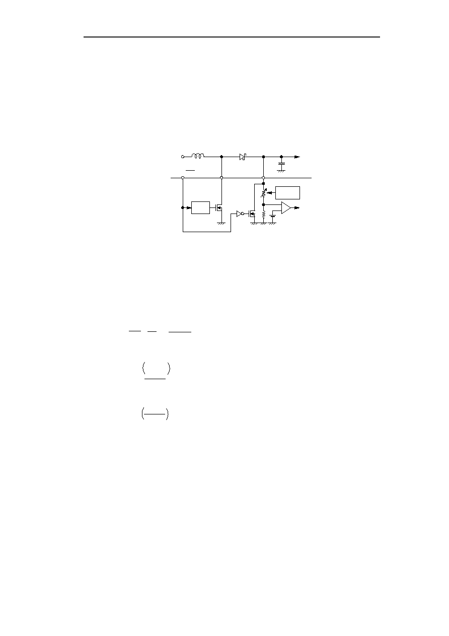
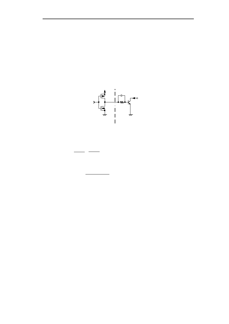
3. Electric Volume
The S-8330/31 series incorporates an electric volume with an 8-bit shift register and an 8-bit latch. The output voltage is
variable in the width of 12 V. The output voltage can be held in the data transmission mode because the data read in the
shift register is fetched into the latch by unshyncronized strobe input. Figure 8 shows a block diagram and timing charts
.
Figure 8 Block Diagram and Timing
VDIN: Inputs data to the electric volume.
"Data 1" is input at "H"level; "Data 0" is input at "Low" level.
VCLK: Inputs clock to the electric volume.
Fetches data at VDIN pin into the shift register at the rising edge of clocks. When clocks of over 8 bits are input,
the read data is shifted in succession for each clock, and data corresponding to 8 bits which was input lastly is
valid.
VSTRB: Inputs strobe signal.
The contents of the shift register are latched by turning the strobe signal to "H. " When the data fetched into the
latch is directly transmitted to the electric volume, the output voltage changes. Data in the latch is held by turning
the strobe signal to "L. "
The electric volume has 8-bit resolution. An
error in linearity may exceed ±1/2LSB (±23.5
mV) only before or after data changeover of
127
128 (01111111
10000000) (see
Figure 9).
The error in linearity corresponds to 6 bits
(±93.8 mV) when used in the 12 V variable
range.
In an application where the variable range
of output voltage is 6 V or less, it is possible to
use it with high linearity accuracy with
appropriate product selection. For example, if
you want to change output voltage within the
range from 12 V to 18 V, select the S-
8330A24FS and use it within the range of
0
127 (00000000
01111111). If so,
high linearity accuracy (within±1/2LSB) can be obtained.
8-bit
Shift Register
RESET
VOUT
VSTRB
VCLK
VDIN
8-bit
Latch
Electric
Volume
D0
D1
D2
D3
D4
D5
D6
D7
(LSB)
Read
Setting
value
Min. value
VOUT
VSTRB
Hold
Reset
Hold
VCLK
VDIN
(MSB)
±
2LSB
(
±
93.8mV)
±
1/2LSB
(
±
23.5mV)
Output Voltage
(V)
Electric
Volume
Data (DEC)
254 255
128
127
0
1
±
1/2LSB
Figure 9 Linearity Accuracy

STEP-UP SWITCHING REGULATOR FOR LCD BIAS SUPPLY
Rev.4.1 S-8330/8331 Series
Seiko Instruments Inc.
13
The contents of the register must be reset because they are uncertain when powering on. If the power off pin is "L" level
and step-up operation stops, the contents of the register are held inside the electric volume by applying voltage of 2 V or
more between V
IN
to V
SS
. Data write and reset operation in the register are also available under this state. The register is
reset by setting VCLK to
H
and VSTRB to "H. " The output voltage is set to the minimum value. Power on under the state
where the power off pin is being set to "L." Next, set VCLK to
H
and VSTRB to "H" to reset the contents of the register.
Then, start step-up operation under the state where the power off pin is being set to "H. "
[
Note
]
If you start step-up operation without resetting the contents of the register after powering on, the maximum voltage is
output to V
OUT
, and the connected device or instrument may be broken or damaged. It is recommended to
connect a pull down resistor to the power off pin if a problem may occur due to the maximum output voltage.
T
Recommended Selection of Series Products and External Parts
1.
How to Select the Series Products
The S-8330/31 Series comes in three types depending upon the switching transistor attachment method (internal or
external) and the oscillating frequency. As shown in Figure 10, respective output current targets differ to ensure high
efficiency within the respective output current range. Select an appropriate series which meets your output current
requirements (see the reference data for the output current and efficiency characteristics).
?
S-8331A Series
:
The switching transistor is externally attached and the oscillating frequency is 180 kHz (typ.). Its target
is the output current of 10 mA or more. High output voltage of 30 V or more is available by only
attaching a simple external circuit to the S-8331A Series (see the S-8330 Series application circuit
shown in Figure 17).
@
S-8330A Series
:
The switching transistor is built in and the oscillating frequency is 180 kHz (typ.). Its target is the
output current ranging from 1 mA to 10 mA. The oscillating frequency of the S-8330A Series is
higher than that of the S-8330B Series. This minimizes ripple and ensures excellent transitory
response characteristics.
A
S-8330B Series
:
The switching transistor is built in and the oscillating frequency is 50 kHz (typ.). Its target is output
current of 1mA or less. The self current consumption of the S-8330B Series is less than that of the
S-8330A Series. This ensures high efficiency in the output current of about 0.1 mA or less.
2.
Inductor
The inductance value greatly affects I
OUT
and efficiency
.
Figure 11 shows the dependency of I
OUT
,
of the S-8330A and the S-8330B on "L."
S-8330B
S-8330A
A switch transistor is built
in
8V
30V
(f=180kHz)
(f=180kHz)
(f=50kHz)
S-8331
A switch transitor is
externally attached
1mA
10mA
100mA
Figure 10 S-8330/8331 Series Depending Upon Output Current
Output
Voltage
Output Current

STEP-UP SWITCHING REGULATOR FOR LCD BIAS SUPPLY
S-8330/8331 Series Rev.4.1
14
Seiko Instruments Inc.
The smaller value L, the larger peak current I
PK
. I
OUT
reaches the maximum value in a certain value L. When decreasing
value L further, the switching transistor falls short of the current drive ability and I
OUT
decreases; when increasing value L, a
loss due to I
PK
of the switching transistor decreases and the efficiency reaches the maximum in a certain value L; when
increasing value L, a loss due to a series resistor of the coils increases. This worsens the efficiency. So, it is recommended
to set value L to 22 to 100
µ
H in the S-8330A and 47 to 220
µ
H in the S-8330B, respectively.
Determine value L referring to the reference data because the maximum output current actually differs depending upon the
input voltage.
Pay attention to the allowable current of the inductor when selecting an appropriate inductor. If current exceeding this
allowable current flows into the inductor, magnetic saturation occurs in the inductor. This may lead to a serious drop in the
efficiency and damage of the IC due to exessive current.
Select an appropriate inductor so that I
PK
does not exceed this allowable current. Current I
PK
in the non-continuous mode is
represented by the following equation.
I
PK
=
, where f
OSC
is the oscillating frequency. Set V
D
to approximately 0.4 V. For example, when you want a power source of input
voltage V
IN
=5 V, output voltage V
OUT
=30 V, and load current I
OUT
=5 mA, the S-8330A30FS responds to your requirements
because f
OSC
=180 kHz. When you set value L to 47
µ
H, I
PK
=174mA is found out as shown in equation (17). As a result, you
can select an inductor for which value L is 47
µ
H and the allowable current is 174 mA or more.
A limitation relating to the maximum value I
PK
lies in the IC itself. Always use current I
PK
at 500 mA or less.
3. Diode
Always use a diode which meets the following conditions.
z
Low forward voltage:
V
F
<0.3V
z
Low switching speed:
500 ns max.
z
Reverse direction voltage:
V
OUT
+V
F
or more
z
Rating current:
I
PK
or more.
2 I
OUT
(V
OUT
+V
D
-V
IN
)
f
OSC
O
L
(A)
(17)
Figure 11 Dependency of Inductance On Maximum Output Current and Efficiency
S-8330A
I
OUT
LQH4N
I
OUT
22
100
Recommended Range
L value (
µ
H
)
V
OUT
=18V, V
IN
=5.0V
S-8330B
I
OUT
LQH4N
I
OUT
47
220
L value (
µ
H
)
V
OUT
=18V, V
IN
=5.0V
Recommended Range
STEP-UP SWITCHING REGULATOR FOR LCD BIAS SUPPLY
Rev.4.1 S-8330/8331 Series
Seiko Instruments Inc.
15
4. Capacitor (C
IN
, C
OUT
)
Capacitor (C
IN
) at the input side improves the efficiency by reducing the power impedance and stabilizing the input current.
Select avalue (C
IN
) depending upon the impedance of the power supply used.
The standard capacitance is approximately 10
µ
F.
Select a capacitor (C
OUT
) at the output side with small ESR (Electric
Series Resistance) and large capacitance to stabilize the ripple voltage. The standard capacitance is approximately 10
µ
F.
It is particularly recommended to use a tantalum electrolytic capacitor with excellent low temperature and leakage current
characteristics.
5. Externally-attached transistors (S-8331 Series)
The output current can be increased by externally attaching a transistor to the S-8331 Series. A bipolar (NPN) type or an
enhancement (Nch) MOS FET type of transistor can be used as an external transistor.
5.1 Bipolar NPN type
Figure 15 shows a circuit example using the 2SD1624 manufactured by SANYO as a bipolar transistor (NPN). The drive
ability to increase output current is determined by values h
FE
and Rb of the bipolar transistor. A peripheral circuit example of
the transistor is shown in Figure 12.
It is recommended to select value Rb of approximately 1k
. Find necessary base current I
b
from the bipolar transistor h
FE
using I
b
=I
PK
/h
FE
,
Rb= -
and select small value Rb. Small value Rb can increase the output current, but may worsen the efficiency. Also current may
flow on the pulse or the voltage may drop due to wiring resistor. So, find the optimum value with experiments.
Attaching a speed-up capacitor Cb to the resistor Rb reduces switching loss and increases the efficiency.
Value Cb:
Cb
5.2 Enhancement MOS FET type
Figure 13 shows a circuit example using the 2SK2159 manufactured by NEC as a MOS FET transistor (Nch). Use an Nch
power MOS FET as a MOS FET. The EXT pin in the S-8331 series can drive a MOS FET with approx.1000 pF gate
capacitance. The ON reisistor of the MOS FET depends upon a difference between voltage input voltage V
IN
and the
threshold voltage of the MOS FET and thereby affects the output amperage and the efficiency. The gate voltage and the
current of the MOS FET are supplied by input voltage V
IN
. So pay attention if the input voltage is low. Also note that the IC
will not function if the threshold voltage of the MOS FET is higher than the input voltage.
Figure 12 External Transistor Peripheral Circuit
Ib
|I
EXTH
|
1
2
◊
Rb
◊
f
OSC
◊
0.7
V
IN
-0.7
0.4
I
PK
EXT
Nch
V
IN
Pch
Rb
S-8331
2200pF
1K
STEP-UP SWITCHING REGULATOR FOR LCD BIAS SUPPLY
S-8330/8331 Series Rev.4.1
16
Seiko Instruments Inc.
RESET
ON/OFF
ZD:15V
R
A
R
B
M
N
2SJ356
SBD
V
OUT
V
SS
V
IN
L
-
+
CL
EXT
2SK2159
T
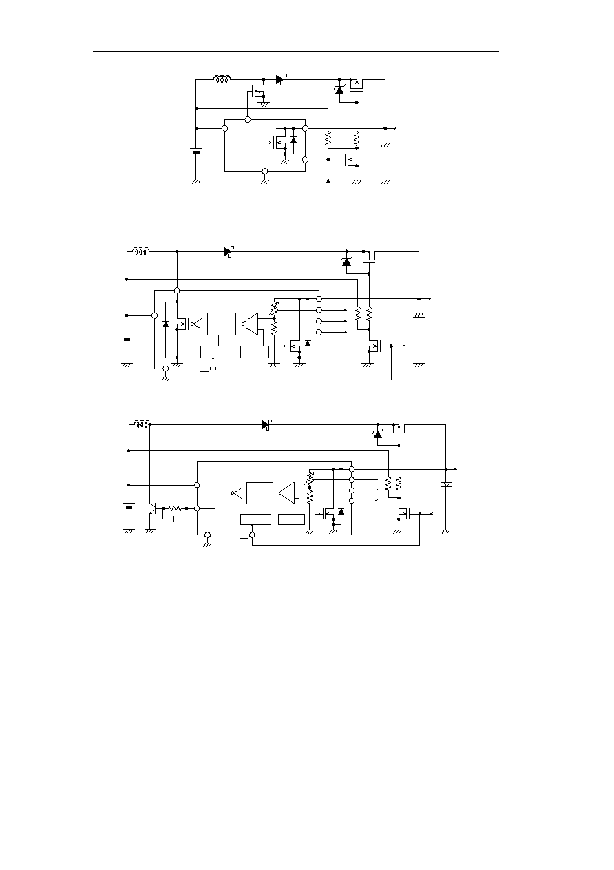
Standard Circuits
CONT
RESET
ON/OFF
ZD
SD
V
OUT
V
SS
CR Oscillator
VREF
PWM
Controller
+
-
V
IN
L
-
+
VDIN
VCLK
VSTRB
CL
Figure 14 S-8330 Series
RESET
ON/OFF
ZD
SD
V
OUT
V
SS
CR
Oscillator
V
REF
PWM
Controller
+
-
-
+
VDIN
VCLK
VSTRB
CL
V
IN
External
Tr
Rb
Cb
EXT
L
Figure 15 S-8331 Series
Figure 13 Circuit Example Using the 2SK2159
(1)
S-8330 Series
(2)
S-8331 Series

STEP-UP SWITCHING REGULATOR FOR LCD BIAS SUPPLY
Rev.4.1 S-8330/8331 Series
Seiko Instruments Inc.
17
T
Design Precautions
z
Mount capacitors, diodes, coils and other components as near as possible to the the IC.
z
Inherent ripple voltage or spike noise may generate in the switching ragulator. Because it greatly depends upon the
coils and the capacitors you use, check it using an actually-mounted model.
z
Make sure that a loss in the switching transistor (particularly at high temperatures) does not exceed the allowable power
dissipation.
Figure 16 8-Pin SSOP Power Dissipation (before mounting)
300
400
200
100
0
0
75
25 50
100 125
Power
Dissipation
P
D
(mW)
Ambient Temperature Ta (∞C)
∑
Configure parts and components so that the line to the VSS pin (indicated by the bold line shown in Figure 17) becomes
short as much as possible. If a resistor and/or an inductance component stays on the line, the VSS potential of the IC
varies depending upon the switching current.
S-8330 Series
CPU
CONT
Vss
Vss
VDIN
VIN
V
OUT
VCLK
VSTRB
ON/OFF
-
Figure 17 S-8330 Series Application Circuit
∑
When switching the output voltage by the electric volume, the soft start does not function. Pay attention to overshoot
occuring when increasing the output voltage with a large width (refer to 5. Output Voltage Changeover shown in the
transitory response characteristics).
∑
Seiko Instruments Inc. shall not be resposible for any patent infringement by products including the S-
8330/8331 Series in connection with the method of using the S-8330/8331 Series in such products, the product
specifications or the country of destination thereof.

STEP-UP SWITCHING REGULATOR FOR LCD BIAS SUPPLY
S-8330/8331 Series Rev.4.1
18
Seiko Instruments Inc.
T
Application Circuits
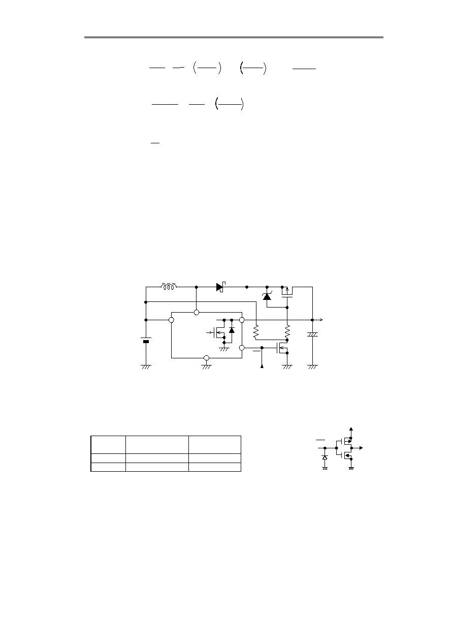
1. Large Size LCD Panel Drive Power Supply
This is a circuit example to drive a large size LCD panel (40 V/20 mA) at a 5-V power (5V±10%).
S-8331A30FS
ON/OFF
Tr.3
Tr.2
Tr.1:
2SD1624
RA:
180k
RB:
600k
ZD:15V
SD:
MA789
To 40V
V
OUT
V
SS
-
+
F93/
4.7
µ
F
◊
2
V
IN
EXT
L
1k
2200pF
VDIN
VCLK
VSTRB
Figure 18 Large Size LCD Panel Drive Power Supply
This is an output voltage step-up circuit using the S-8331 Series. 30 V or more output voltage, i.e., the maximum voltage
of the S-8330/8331 Series, is available by dividing the output voltage by external resistors RA and RB and feeding back to
V
OUT
pin. In the S-8331 Series the internal impedance of V
OUT
pin varies by switching the electric volume. Therefore, a
small singal NPN transistor (Tr. 3) is needed between the external voltage dividing resistor and V
OUT
pin to convert the
impedance.
The output voltage is represented by equation (18).
Output voltage =
(V
OUT
+V
BE
) (18)
V
OUT
: S-8331 V
OUT
setting voltage
V
BE
: Voltage between the base and the emitter of Tr. 3
Pay attention to the following precautions when using this IC.
∑
Make sure that the switching transistor (Tr.1) and a Schottky diode (SD) have sufficient resistance against high output
voltage you use. For example, the 2SD1624 manufactured by Sanyo and the MA789 manufactured by Matsushita are
used in this circuit example for a switching transistor and a Schottky diode, respectively.
∑
When stopping step-up operation from the step-up operation state using the power off pin, V
OUT
pin is short-circuited to
V
SS
by an Nch transistor. Because of this, the output voltage is temporarily added to the area between the collector and
the emitter of the transistor (Tr. 3). Always use a small signal transistor which is sufficient enough to withstand high
output voltage (Tr. 3).
∑
The output voltage fails to stabilize when the output current falls short to 1 mA or less. In this case, add a capacitor CF
between the output line and the V
OUT
pin. The recommended capacitance of the capacitor is approx. 0.01uF. Select the
best capacitance after checking it under actual operation conditions.
2. Medium Size LCD Panel Drive Power Supply for PDA
Voltage suitable for smart addressing (SA) and multiple line addressing (A) drive generates from a 3V- or 5 V-power supply.
The following is a circuit example and its characteristics, targeted at positive voltage of approx. +15V/500
µ
A and negative
voltage of approx. -9V/500
µ
A.
CONT
S-8330B
Vss
VDIN
V
IN
V
OUT
VCLK
VSTRB
ON/OFF
-
+
-
+
-
+
VIN
F93
Co+
#O
/10
µ
Sumida/
10
20
12
+15V
-9V
MA720
MA720
100
µ
H
/10
µ
F93
/10
µ
F93
CEE93
+VOUT
-VOUT
VOUT=15V
Set
1
st
side
3rd
2
nd
side
Figure 19 Medium Size LCD Panel Drive Power Supply for PDA
RA + RB
RB

STEP-UP SWITCHING REGULATOR FOR LCD BIAS SUPPLY
Rev.4.1 S-8330/8331 Series
Seiko Instruments Inc.
19
Output Vol.
VOUT (V)
14.6
14.8
15.0
15.2
15.4
0.01
0.1
1
10
100
Output Current I
OUT
(mA)
V
OUT
=+15V
VIN=2.8V
VIN=3.8V
VIN=5.0V
Output Current - Output voltage characteristics (Output Current Increase)
Output Current - Output Voltage Characteristics (Output Current Increase)
-9.4
-9.2
-9.0
-8.8
-8.6
0.01
0.1
1
10
100
VIN=2.8V
VIN=3.8V
VIN=5.0V
V
OUT
=-9V
Output Vol.
VOUT (V)
Output Current I
OUT
(mA)
40
50
60
70
80
90
0.01
0.1
1
10
100
VIN=2.8V
VIN=3.8V
VIN=5.0V
Output Current - Efficiency Characteristics (Output Current Increase)
Efficiency
(%)
Output Current I
OUT
(mA)
This circuit stablilizes the positive output voltage +VOUT in the S-8330B Series. The negative output voltage -VOUT is
determined and stabilized by the wiring ratio at the second and third sides in the transducer manufactured by Sumida
(CEE93 6375-002 non-gap type) when the output current at the positive side is the same as that at the negative side. Also
this circuit is targeted at applications at low load. The use of a 50 kHz product with low switching frequency improves the
efficiency at load of approx. 500mA.
Pay attention to the following precautions when using it.
∑
Generally, the allowable current level of the thin transducer (CEE93 equivalent) is lower than that of the thin coil (CD54
equivalent). Make sure that the current flowing into the transducer under the specified operational conditions does not
exceed the allowable current. For example, if load current is larger than 5 mA in the above circuit, magnetic saturation
occurs and the IC may be damaged at the worst.
∑
When using an external gap-type transducer, the stability in the negative output voltage may worsen.
For external parts, contact
Sumida Electric Co., Ltd.
Technical Sales & Support Center
3-3-6, Nihonbashi Ningyo-cho, Chuo-ku, Tokyo, 103-8589
TEL:03-3667-3320 FAX:03-3667-3409
For comprehensive inquiry, consult with
SII Components Sales Dept.
TEL:043-211-1192 (Direct) FAX:043-211-8032
STEP-UP SWITCHING REGULATOR FOR LCD BIAS SUPPLY
S-8330/8331 Series Rev.4.1
20
Seiko Instruments Inc.
T
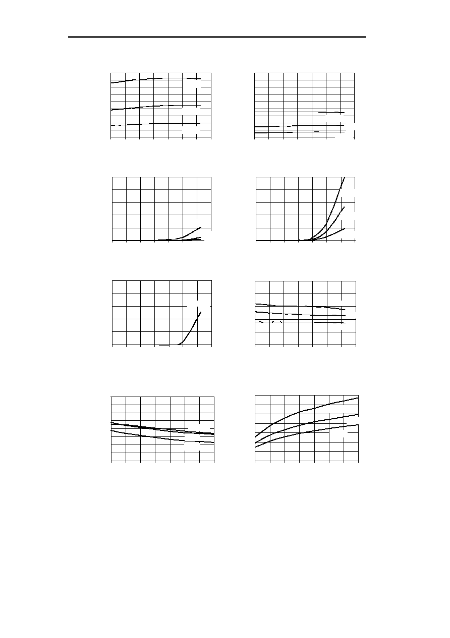
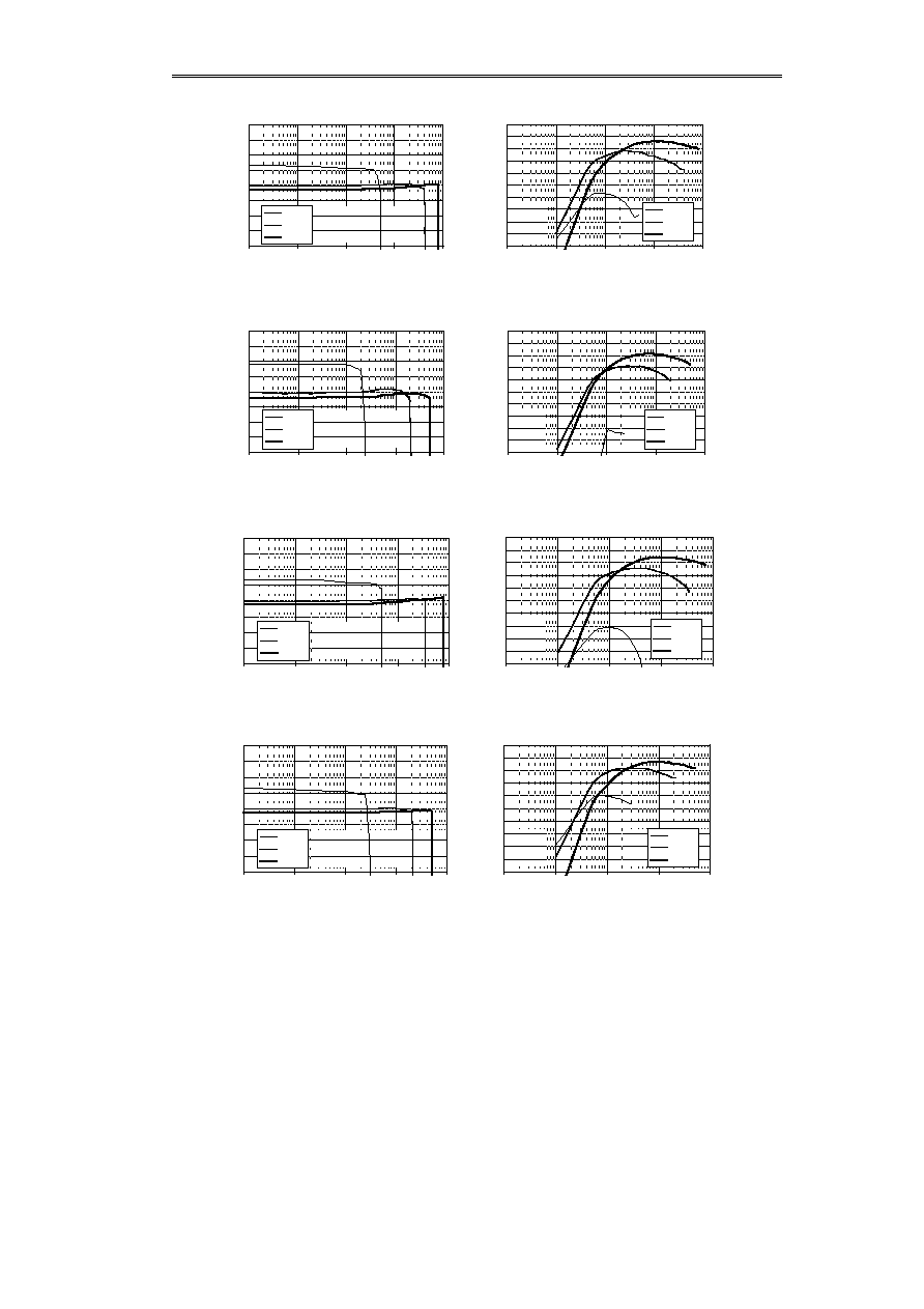
Temperature Characteristics
I
SS1
,I
SS2
-- Temp
S-8330A
0
20
40
60
80
100
120
140
160
180
-40
-20
0
20
40
60
80
100
Ta (∫C)
I
SS1
(
µ
A)
I
SS1
:V
IN
=2V,V
OUT
=8V I
SS2
:V
IN
=5V,V
OUT
=30V
V
IN
=9V
V
IN
=5V
V
IN
=2V
I
SS1
,I
SS2
-- Temp
S-8331A
0
20
40
60
80
100
120
140
160
180
-40
-20
0
20
40
60
80
100
Ta (∫C)
I
SS1
(
µ
A)
I
SS1
:V
IN
=2V,V
OUT
=8V I
SS2
:V
IN
=5V,V
OUT
=30V
V
IN
=9V
V
IN
=5V
V
IN
=2V
I
SSS
-- Temp
S-8330A
0.00
0.02
0.04
0.06
0.08
0.10
-40
-20
0
20
40
60
80
100
Ta (
∞
C)
I
SSS
(
µ
A)
V
IN
=9V
V
IN
=5V
V
IN
=2V
I
SSS
-- Temp
S-8331A
0.00
0.02
0.04
0.06
0.08
0.10
-40
-20
0
20
40
60
80
100
Ta (
∞
C)
I
SSS
(
µ
A)
V
IN
=9V
V
IN
=5V
V
IN
=2V
I
SWQ
-- Temp
S-8330A/B
0.00
0.02
0.04
0.06
0.08
0.10
-40
-20
0
20
40
60
80
100
Ta (
∞
C)
I
SWQ
(
µ
A)
V
IN
=2,5,9V
MaxDuty -- Temp
S-8330A/31A
50
60
70
80
90
100
-40
-20
0
20
40
60
80
100
Ta (
∞
C)
MaxDuty
(%)
V
IN
=2V
V
IN
=5V
V
IN
=9V
VOUT=18V
T
Power Supply Dependency Characteristics
F
OSC
-- V
IN
S-8330A/31A
140
150
160
170
180
190
200
210
220
2
3
4
5
6
7
8
9
VIN (V)
F
OSC
(kHz)
Ta=-40
Ta=85
Ta=25
I
SW
-- V
IN
S-8330A/B
0
50
100
150
200
250
300
350
2
3
4
5
6
7
8
9
VIN (V)
I
SW
(mA)
V
OUT
=18V
Ta=-40
Ta=85
Ta=25
STEP-UP SWITCHING REGULATOR FOR LCD BIAS SUPPLY
Rev.4.1 S-8330/8331 Series
Seiko Instruments Inc.
21
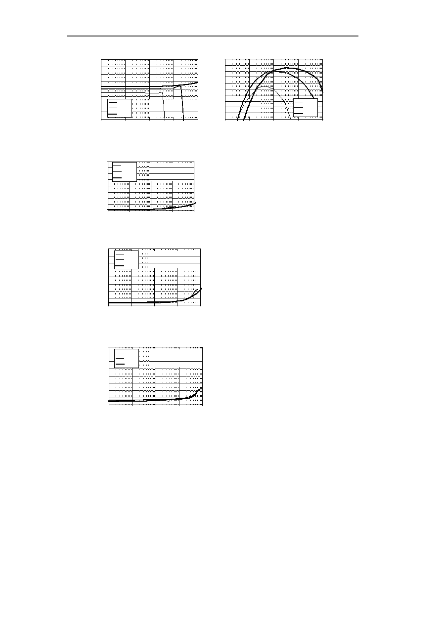
I
EXTH
-- V
IN
S-8331A
0
1
2
3
4
5
6
7
8
9
10
2
3
4
5
6
7
8
9
V
IN
(V)
I
EXTH
(mA)
Ta=-40
Ta=85
Ta=25
I
EXTL
-- V
IN
S-8331A
0
1
2
3
4
5
6
7
8
9
10
2
3
4
5
6
7
8
9
V
IN
(V)
I
EXTL
(mA)
Ta=-40
Ta=85
Ta=25
V
SH1,2
-- V
IN
S-8330A/B/31A
0.60
0.80
1.00
1.20
1.40
1.60
2
3
4
5
6
7
8
9
V
IN
(V)
V
SH1,2
(V)
Ta=-40
Ta=25
Ta=85
VSL -- VIN
S-8330A/B/31A
0.40
0.50
0.60
0.70
0.80
0.90
2
3
4
5
6
7
8
9
V
IN
(V)
V
SL
(V)
Ta=85
Ta=25
Ta=-40
V
SHC1,2
-- V
IN
S-8330A/B/31A
0.60
0.80
1.00
1.20
1.40
1.60
2
3
4
5
6
7
8
9
V
IN
(V)
V
SHC1,2
(V)
Ta=85
Ta=25
Ta=-40
V
SHL
-- V
IN
S-8330A/B/31A
0.40
0.50
0.60
0.70
0.80
0.90
2
3
4
5
6
7
8
9
V
IN
(V)
V
SHL
(V)
Ta=85
Ta=25
Ta=-40
STEP-UP SWITCHING REGULATOR FOR LCD BIAS SUPPLY
S-8330/8331 Series Rev.4.1
22
Seiko Instruments Inc.
T
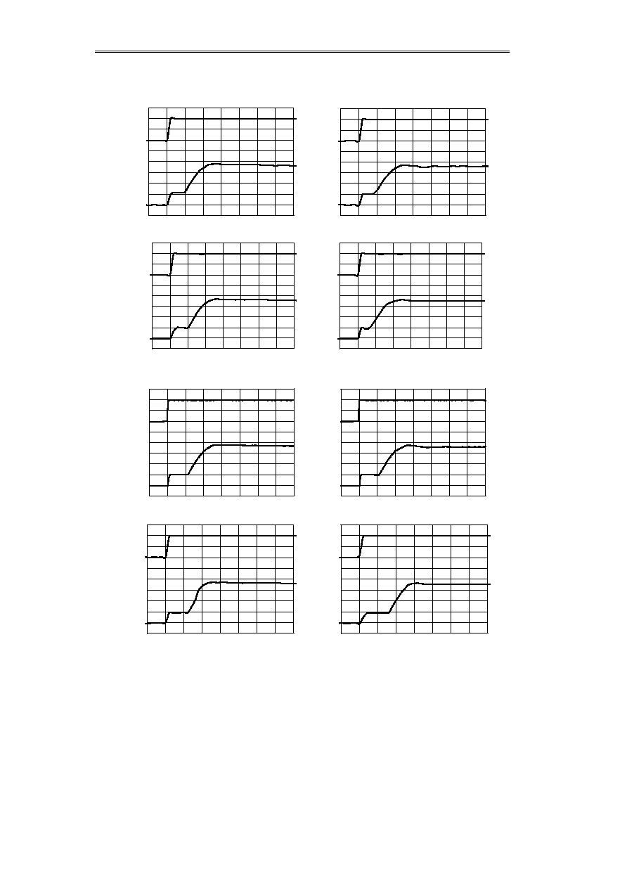
Transitory Response Characteristics
1. Powering On (V
IN
: OV
5.OV)
S-8330A30 (Light Load : I
OUT
=1mA)
t (1msec/div)
Output Vol.
(5V/div)
Input Vol.
(2.5V/div)
V
OUT
=18V
0V
20V
0V
5V
t (1msec/div)
Output Vol.
(5V/div)
Input Vol.
(2.5V/div)
V
OUT
=18V
0V
20V
0V
5V
S-8330A30 (Heavy Load : I
OUT
=1mA)
S-8331A30 (Light Load
I
OUT
=1mA)
t (1msec/div)
Output Vol.
(5V/div)
Input Vol.
(2.5V/div)
V
OUT
=18V
0V
20V
0V
5V
S-8331A30 (Heavy Load
I
OUT
=20mA)
t (1msec/div)
Output Vol.
(5V/div)
Input Vol.
(2.5V/div)
V
OUT
=18V
0V
20V
0V
5V
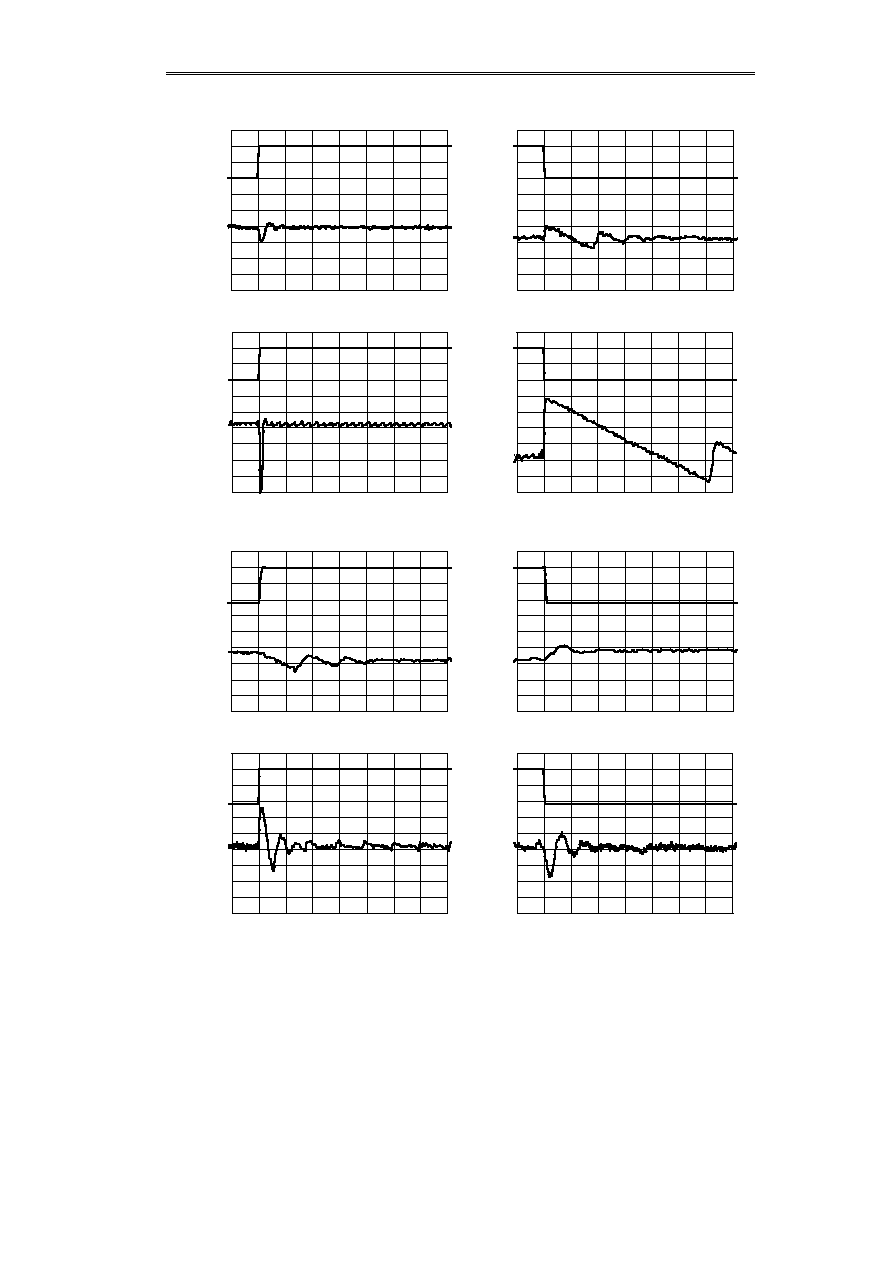
2.Power Off Pin Response (Von/off=0
5.OV)
S-8330A30 (Light Load : I
OUT
=1mA)
t (1msec/div)
Output Vol.
(5V/div)
Power off
Pin Voltage
V
IN
=5V,V
OUT
=18V
0V
20V
0V
5V
S-8330A30 (Heavy Load : I
OUT
=10mA)
t (1msec/div)
Output Vol.
(5V/div)
0V
20V
0V
5V
V
IN
=5V,V
OUT
=18V
Power off
Pin Voltage
S-8331A30 (Light Load
I
OUT
=1mA)
t (1msec/div)
Output Vol.
(5V/div)
Power off
Pin Voltage
V
IN
=5V,V
OUT
=18V
0V
20V
0V
5V
S-8331A30 (Heavy Load
OUT
=20mA)
t (1msec/div)
Output Vol.
(5V/div)
Power off
Pin Voltage
0V
20V
0V
5V
V
IN
=5V,V
OUT
=18V
STEP-UP SWITCHING REGULATOR FOR LCD BIAS SUPPLY
Rev.4.1 S-8330/8331 Series
Seiko Instruments Inc.
23
3.Load Variations
S-8330A30 ( I
OUT
:0.01m
1mA)
t (5msec/div)
Output Vol.
(50mV/div)
Load Current
V
IN
=5V,V
OUT
=18V
S-8330A30 ( I
OUT
:1mA
0.01mA)
t (5msec/div)
Output Vol.
(50mV/div)
Load Current
V
IN
=5V,V
OUT
=18V
S-8331A30 ( I
OUT
:0.01mA
1mA)
t (5msec/div)
Output Vol.
(50mV/div)
Load Current
V
IN
=5V,V
OUT
=18V
S-8331A30 ( I
OUT
:1mA
0.01mA)
t (5msec/div)
Output Vol.
(50mV/div)
Load Current
V
IN
=5V,V
OUT
=18V
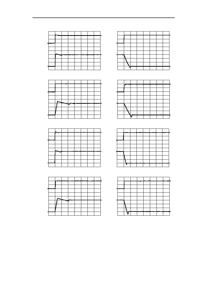
4. Power Supply Variations
S-8330A30 ( VIN:2.4V
3.5V)
t (5msec/div)
Output Vol.
(50mV/div)
Input Vol.
(0.5V/div)
I
OUT
=1mA,V
OUT
=18V
S-8330A30 ( VIN:3.5V
2.4V)
t (5msec/div)
Output Vol.
(50mV/div)
Input Vol.
(0.5V/div)
I
OUT
=1mA,V
OUT
=18V
S-8331A30 ( V
IN
:2.4V
3.5V)
t (5msec/div)
Output Vol.
(50mV/div)
Input Vol.
(0.5V/div)
I
OUT
=1mA,V
OUT
=18V
S-8331A30 ( V
IN
:3.5V
2.4V)
t (5msec/div)
Output Vol.
(50mV/div)
Input Vol.
(0.5V/div)
I
OUT
=1mA,V
OUT
=18V
STEP-UP SWITCHING REGULATOR FOR LCD BIAS SUPPLY
S-8330/8331 Series Rev.4.1
24
Seiko Instruments Inc.
5. Output Voltage Changeover
S-8330A20 (V
OUT
:8V
14V)
t (5msec/div)
Output Vol.
(2V/div)
STRB
Pin Vol.
V
IN
=5V, I
OUT
=1mA
8V
14V
0V
5V
S-8330A20 (V
OUT
:14V
8V)
t (5msec/div)
Output Vol.
(2V/div)
STRB
Pin Vol.
V
IN
=5V, I
OUT
=10mA
8V
14V
0V
5V
S-8330A30 (V
OUT
:18V
24V)
t (5msec/div)
Output Vol.
(2V/div)
STRB
Pin Vol.
V
IN
=5V, I
OUT
=1mA
18V
24V
0V
5V
S-8330A30 (V
OUT
:24V
18V)
t (5msec/div)
Output Vol.
(2V/div)
STRB
Pin Vol.
V
IN
=5V, I
OUT
=10mA
18V
24V
0V
5V
S-8331A20 (V
OUT
:8V
14V)
t (5msec/div)
Output Vol.
(2V/div)
STRB
Pin Vol.
V
IN
=5V, I
OUT
=1mA
8V
14V
0V
5V
S-8331A20 (V
OUT
:14V
8V)
t (5msec/div)
Output Vol.
(2V/div)
STRB
Pin Vol.
V
IN
=5V, I
OUT
=20mA
8V
14V
0V
5V
S-8331A30 (V
OUT
:18V
24V)
t (5msec/div)
Output Vol.
(2V/div)
STRB
Pin Vol.
V
IN
=5V, I
OUT
=1mA
18V
24V
0V
5V
S-8331A30 (V
OUT
:24V
18V)
t (5msec/div)
Output Vol.
(2V/div)
STRB
Pin Vol.
V
IN
=5V, I
OUT
=20mA
18V
24V
0V
5V

STEP-UP SWITCHING REGULATOR FOR LCD BIAS SUPPLY
Rev.4.1 S-8330/8331 Series
Seiko Instruments Inc.
25
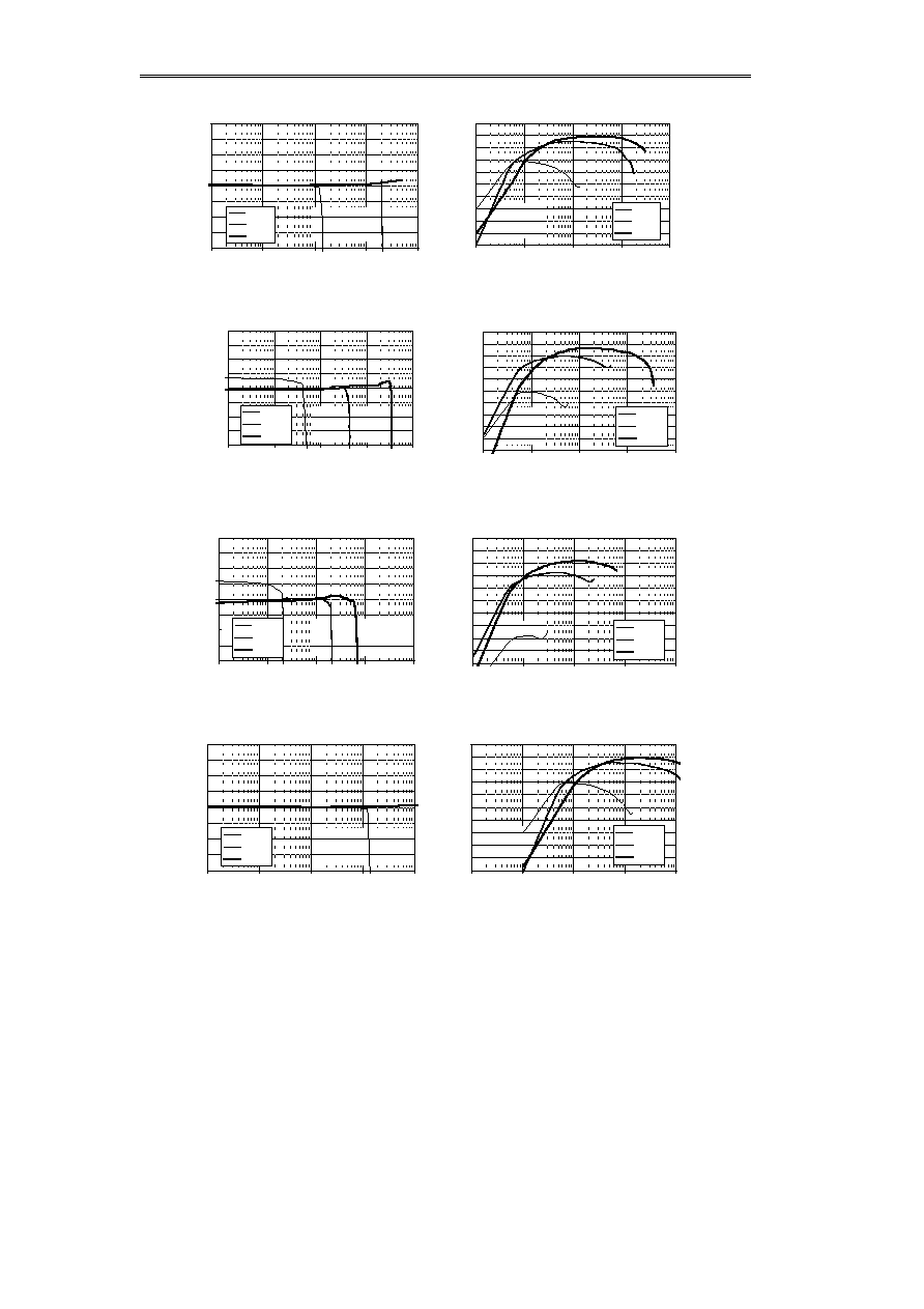
T
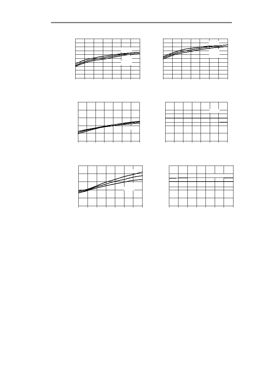
Reference Data
The reference data is used to properly determine the best external parts. Tables 1 and 2 list characteristic data of parts
recommended to respond to the wide variety of applications.
Table 1 Recommended Parts 1
No.
Product
V
OUT
L model
Value L
Diode
C
OUT
Remark
(1)
(2)
(3)
(4)
(5)
(6)
(7)
(8)
(9)
(10)
(11)
(12)
(13)
S-8330A20
S-8330A30
S-8330A20
S-8330A30
S-8330B30
S-8330A20
S-8330A30
S-8330B30
8V
18V
30V
8V
18V
30V
18V
8V
18V
30V
18V
CD54
LQH4N
CD54
LQH4N
47
µ
H
22
µ
H
100
µ
H
100
µ
H
47
µ
H
100
µ
H
MA720
4.7
µ
F
◊
2
Output current, Efficiency
Ripple voltage
Table 2 Recommended Parts 2
Part
Product
Manufacturer
Value L
DC resistor
Max. p. c.
Diameter
Height
CD54
Sumida Electric
22
µ
H
0.18
1.11A
5.8mm
4.5mm
47
µ
H
0.37
0.72A
100
µ
H
0.70
0.52A
Inductor
LQH4N
Murata Mfg.
22
µ
H
0.94
0.32A
4.5mm
2.6mm
47
µ
H
1.5
0.22A
100
µ
H
2.5
0.16A
220
µ
H
5.4
0.11A
Diode
MA720
Matsushita
Forward current 500 mA (VF=0.55 V)
Output capacitor
F93
Nichicon
External transistor
2SD1624
Sanyo Electric
STEP-UP SWITCHING REGULATOR FOR LCD BIAS SUPPLY
S-8330/8331 Series Rev.4.1
26
Seiko Instruments Inc.
(1)
7.6
7.8
8.0
8.2
8.4
0.1
1
10
100
1000
Output Current I
OUT
(mA)
VIN=2V
VIN=5V
VIN=7V
V
OUT
=8V
S-8330A20 (CD54:47
µ
H)
Output Current -- Output Voltage Characteristics (Output Current Increase)
Output Vol.
V
OUT
(V)
50
60
70
80
90
100
0.1
1
10
100
1000
Output Current I
OUT
(mA)
VIN=2V
VIN=5V
VIN=7V
V
OUT
=8V
S-8330A20 (CD54:47
µ
H)
Output Current -- Efficiency Characteristics (Output Current Increase)
Efficiency
(%)
(2)
17.6
17.8
18.0
18.2
18.4
0.1
1
10
100
1000
Output Current I
OUT
(mA)
VIN=2V
VIN=5V
VIN=9V
V
OUT
=18V
Output Vol.
V
OUT
(V)
S-8330A30 (CD54:47
µ
H)
Output Current -- Output Voltage Characteristics (Output Current Increase)
50
60
70
80
90
100
0.1
1
10
100
1000
Output Current I
OUT
(mA)
VIN=2V
VIN=5V
VIN=9V
V
OUT
=18V
S-8330A30 (CD54:47
µ
H)
Output Current -- Efficiency Characteristics (Output Current Increase)
Efficiency
(%)
(3)
29.6
29.8
30.0
30.2
30.4
0.1
1
10
100
1000
Output Current I
OUT
(mA)
VIN=2V
VIN=5V
VIN=9V
V
OUT
=30V
S-8330A30 (CD54:47
µ
H)
Output Current -- Output Voltage Characteristics (Output Current Increase)
Output Vol.
V
OUT
(V)
50
60
70
80
90
100
0.1
1
10
100
1000
Output Current I
OUT
(mA)
VIN=2V
VIN=5V
VIN=9V
V
OUT
=30V
S-8330A30 (CD54:47
µ
H)
Output Current -- Efficiency Characteristics (Output Current Increase)
Efficiency
(%)
(4)
7.6
7.8
8.0
8.2
8.4
0.01
0.1
1
10
100
Output Current I
OUT
(mA)
VIN=2V
VIN=5V
VIN=7V
V
OUT
=8V
S-8330A20 (LQH4N:47
µ
H)
Output Current -- Output Voltage Characteristics (Output Current Increase)
Output Vol.
V
OUT
(V)
50
60
70
80
90
100
0.01
0.1
1
10
100
Output Current I
OUT
(mA)
VIN=2V
VIN=5V
VIN=7V
V
OUT
=8V
S-8330A20 (LQH4N:47
µ
H)
Output Current -- Efficiency Characteristics (Output Current Increase)
Efficiency
(%)
STEP-UP SWITCHING REGULATOR FOR LCD BIAS SUPPLY
Rev.4.1 S-8330/8331 Series
Seiko Instruments Inc.
27
(5)
17.6
17.8
18.0
18.2
18.4
0.01
0.1
1
10
100
Output Current I
OUT
(mA)
VIN=2V
VIN=5V
VIN=9V
V
OUT
=18V
S-8330A30 (LQH4N:47
µ
H)
Output Current -- Output Voltage Characteristics (Output Current Increase)
Output Vol.
V
OUT
(V)
50
60
70
80
90
100
0.01
0.1
1
10
100
Output Current I
OUT
(mA)
VIN=2V
VIN=5V
VIN=9V
V
OUT
=18V
S-8330A30 (LQH4N:47
µ
H)
Output Current -- Ef f iciency Characteristics (Output Current Increase)
Eff iciency
(%)
(6)
29.6
29.8
30.0
30.2
30.4
0.01
0.1
1
10
100
Output Current I
OUT
(mA)
VIN=2V
VIN=5V
VIN=9V
V
OUT
=30V
S-8330A30 (LQH4N:47
µ
H)
Output Current -- Output Voltage Characteristics (Output Current Increase)
Output Vol.
V
OUT
(V)
50
60
70
80
90
100
0.01
0.1
1
10
100
Output Current I
OUT
(mA)
VIN=2V
VIN=5V
VIN=9V
V
OUT
=30V
S-8330A30 (LQH4N:47
µ
H)
Output Current -- Efficiency Characteristics (Output Current Increase)
Efficiency
(%)
(7)
17.6
17.8
18.0
18.2
18.4
0.01
0.1
1
10
100
Output Current I
OUT
(mA)
VIN=2V
VIN=5V
VIN=9V
V
OUT
=18V
S-8330A30 (LQH4N:22
µ
H)
Output Current -- Output Voltage Characteristics (Output Current Increase)
Output Vol.
V
OUT
(V)
50
60
70
80
90
100
0.01
0.1
1
10
100
Output Current I
OUT
(mA)
VIN=2V
VIN=5V
VIN=9V
V
OUT
=18V
S-8330A30 (LQH4N:22
µ
H)
Output Current -- Efficiency Characteristics (Output Current Increase)
Efficiency
(%)
(8)
17.6
17.8
18.0
18.2
18.4
0.01
0.1
1
10
100
Output Current I
OUT
(mA)
VIN=2V
VIN=5V
VIN=9V
V
OUT
=18V
S-8330A30 (LQH4N:100
µ
H)
Output Current -- Output Voltage Characteristics (Output Current Increase)
Output Vol.
V
OUT
(V)
50
60
70
80
90
100
0.01
0.1
1
10
100
Output Current I
OUT
(mA)
VIN=2V
VIN=5V
VIN=9V
V
OUT
=18V
S-8330A30 (LQH4N:100
µ
H)
Output Current -- Efficiency Characteristics (Output Current Increase)
Efficiency
(%)
STEP-UP SWITCHING REGULATOR FOR LCD BIAS SUPPLY
S-8330/8331 Series Rev.4.1
28
Seiko Instruments Inc.
(9)
17.6
17.8
18.0
18.2
18.4
0.01
0.1
1
10
100
Output Current I
OUT
(mA)
VIN=2V
VIN=5V
VIN=9V
V
OUT
=18V
S-8330B30 (LQH4N:100
µ
H)
Output Current -- Output Voltage Characteristics (Output Current Increase)
Output Vol.
V
OUT
(V)
50
60
70
80
90
100
0.01
0.1
1
10
100
Output Current I
OUT
(mA)
VIN=2V
VIN=5V
VIN=9V
V
OUT
=18V
S-8330B30 (LQH4N:100
µ
H)
Output Current -- Efficiency Characteristics (Output Current Increase)
Efficiency
(%)
(10)
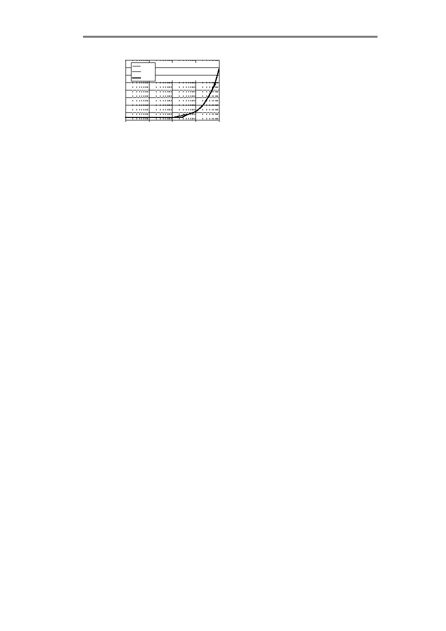
00
0
50
100
150
200
0.01
0.1
1
10
100
Output Current I
OUT
(mA)
VIN=2V
VIN=5V
VIN=7V
V
OUT
=8V
S-8330A20 (CD54:47
µ
H)
Output Current -- Ripple Voltage Characteristics (Output Current Increase)
Ripple
Voltage
Vr (mV)
(11)
0
50
100
150
200
0.01
0.1
1
10
100
Output Current I
OUT
(mA)
VIN=2V
VIN=5V
VIN=9V
V
OUT
=18V
S-8330A30 (CD54:47
µ
H)
Output Current -- Ripple Voltage Characteristics (Output Current Increase)
Ripple
Voltage
Vr (mV)
(12)
0
50
100
150
200
0.01
0.1
1
10
100
Output Current I
OUT
(mA)
VIN=2V
VIN=5V
VIN=9V
V
OUT
=30V
S-8330A30 (CD54:47
µ
H)
Output Current -- Ripple Voltage Characteristics (Output Current Increase)
Ripple
Voltage
Vr (mV)
STEP-UP SWITCHING REGULATOR FOR LCD BIAS SUPPLY
Rev.4.1 S-8330/8331 Series
Seiko Instruments Inc.
29
(13)
0
50
100
150
200
0.01
0.1
1
10
100
Output Current IOUT(mA)
VIN=2V
VIN=5V
VIN=9V
V
OUT
=18V
S-8330B30 (LHQ4N:100
µ
H)
Output Current -- Ripple Voltage Characteristics (Output Current Increase)
Ripple
Voltage
Vr (mV)
(4.0)
6.9 0.1
1.4 0.1
0.3 0.05
1.55 0.05
1.55 0.05
4.0 0.1
2.0 0.05
8-pin SSOP
FS008-A 990531
0.22±0.1
0.65
3.1±0.3
1
8
5
4
R135
13.5 0.5
Winding core
Unit:mm
Dimensions
Taping Specifications
Reel Specifications
1 reel holds 2000 ICs.

Markings
990603
8330
8-pin SSOP
1
4
2
3
8
7
9
6
5
(10)

∑
The information described herein is subject to change without notice.
∑
Seiko Instruments Inc. is not responsible for any problems caused by circuits or diagrams described herein
whose related industrial properties, patents, or other rights belong to third parties. The application circuit
examples explain typical applications of the products, and do not guarantee the success of any specific
mass-production design.
∑
When the products described herein are regulated products subject to the Wassenaar Arrangement or other
agreements, they may not be exported without authorization from the appropriate governmental authority.
∑
Use of the information described herein for other purposes and/or reproduction or copying without the
express permission of Seiko Instruments Inc. is strictly prohibited.
∑
The products described herein cannot be used as part of any device or equipment affecting the human
body, such as exercise equipment, medical equipment, security systems, gas equipment, or any apparatus
installed in airplanes and other vehicles, without prior written permission of Seiko Instruments Inc.
∑
Although Seiko Instruments Inc. exerts the greatest possible effort to ensure high quality and reliability, the
failure or malfunction of semiconductor products may occur. The user of these products should therefore
give thorough consideration to safety design, including redundancy, fire-prevention measures, and
malfunction prevention, to prevent any accidents, fires, or community damage that may ensue.