Document Outline
- Main Menu
- S-8335 Series
- COVER
- Features
- Applications
- Package Name
- Block Diagram
- Selection Guide
- Pin Assignment
- Absolute Maximum Ratings
- Electrical Characteristics
- Recommended Peripheral Parts (When VICON=1.6 V)
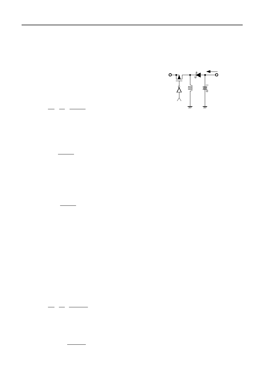
- Measurement Circuits
- Operation
- Operation Modes and Mode Control
- Electric volume
- OP amplifier X
- OP amplifier Y
- Regulator S Part
- Regulator T Part
- Power Supply Rising Edge Sequence
- Soft Start
- Selection of External Parts
- Standard Circuits
- Pattern Diagram
- Application Circuit
- Precautions
- Characteristic Curves
- Package Drawing

Rev.5.2
Seiko Instruments Inc.
1
Positive and Negative Voltage Three-channel Switching
Regulator for LCD Bias Supply
S-8335 Series
The S-8335 Series is a bias supply IC for a Multi Line Addressing (MLA)
driven LCD using a dual-line simultaneous selection mode. This IC
supports medium-sized LCD panels. Two step-up type and one inverter
type PFM control CMOS switching regulators supply the required positive or
negative power to the two MLA-driven LCD common drivers and segment
drivers. Because of its CMOS structure, the current consumption of the S-
8335 Series is extremely low, which makes it ideal for the LCD power
supply of portable equipment that requires low power consumption. Also,
an extremely low power consumption LCD module can be created by using
the S-8335 Series with the LCD common driver (HD66523R
1
:
Manufactured by Hitachi, Ltd.) and segment driver (HD66522
1
:
Manufactured by Hitachi, Ltd.).
1:These drivers are able to support 1/240duty and 1/200duty.
Features
∑
Supports four types of LCD panels (1/240 duty, 1/200 duty, 1/160 duty, and 1/120 duty).
∑
Input voltage range: 2.4 to 5.0 V (The S-8335 can be driven by a single direct-coupled lithium battery.)
∑
Output voltage range
Common driver positive power supply (VRH) output voltage range(typ.value)
8.91 to 16.59 V (S-8335A240FT)
8.22 to 15.30 V (S-8335A200FT)
7.48 to 13.93 V (S-8335A160FT)
6.66 to 12.41 V (S-8335A120FT)
(This supply can be varied by on-chip 6-bit electric volume. Power MOSFET is built in.)
Common driver negative power supply (VRL) output voltage range(typ.value)
-6.87 to -12.80 V (S-8335A240FT)
-6.18 to -11.49 V (S-8335A200FT)
-5.44 to -10.13 V (S-8335A160FT)
-4.61 to -8.59 V (S-8335A120FT)
Segment driver positive power supply (VCH) output voltage range 2.0 to 3.8 V
Segment driver intermediate potential (VM) output voltage range 1.0 to 1.9 V
Icon positive power supply (VICON) output voltage range 1.0 to 2.2 V (This supply can be set arbitrarily
by external resistors.)
∑
Low current consumption
100
µ
A typ. (mode 1, V
BAT
= 3 V)
10
µ
A typ. (mode 2, V
BAT
= 3 V)
1
µ
A max. (mode 3, V
BAT
= 3 V)
∑
Triple operation mode function: Triple mode switching according to 2-bit input
Mode 1: Normal operation
Mode 2: Icon mode (reference voltage circuit- and regulator S-only operation)
Mode 3: Standby mode (power off)
∑
Power-off function
Stops step-up or step-down operation and short circuits VRH and VRL to VSS by on-chip and external
Nch transistors.
∑
Soft-start function: This function can be set according to an external capacitor (CSS).
∑
Oscillation frequency: 100 kHz
±
20 kHz, Duty = 50%
Applications
∑
Power supply for medium-sized LCD panel
Package Name
∑
24-pin TSSOP package (PKG diagram code: FT024-A)
Positive and Negative Voltage Three-channel Switching Regulator for LCD Bias Supply
S-8335 Series
Rev.5.2
Seiko Instruments Inc.
2
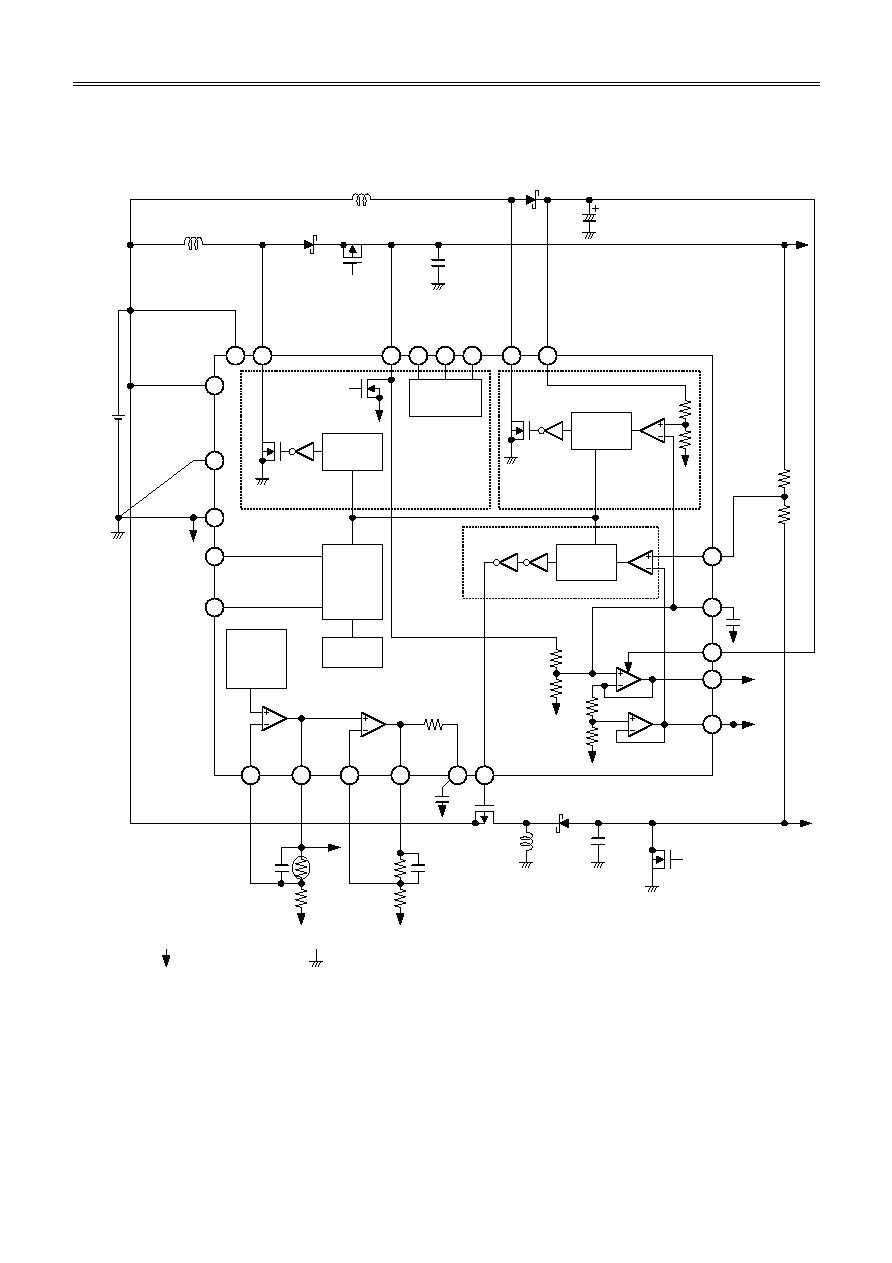
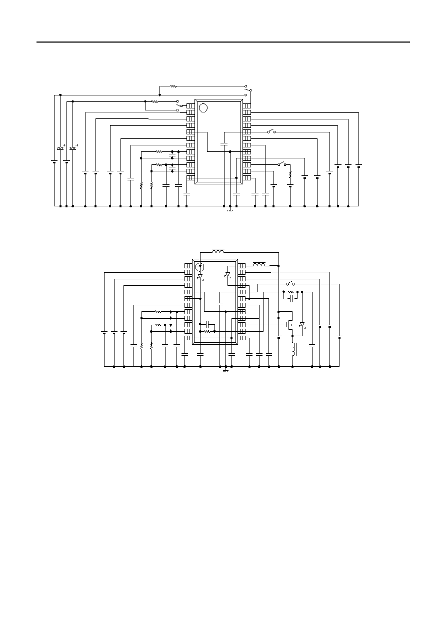
Block Diagram
12
1
6
2
3
24
4
21
VD
IN
VC
L
K
VSTR
_
B
VO
U
T
3
CONT
3
CONT
1
VO
U
T
1
: small current VSS,
:
large current VSS
16
5
17
23
22
10
11
8
9
7
15
13
14
20
19
18
VREGTF VREGTO
VREGSF
RT1
RT2
CRT1
CRS1
CSS
F
L2
D2
CL2
EXT2
VICON
VREGSO
VYO
MC2
VBAT
MC1
VQERR
VXO
VDDX
CREFU
VREFU
Electric
volume
DC/DC P
DC/DC U
DC/DC Q
op-amp X
op-amp Y
REG T
REG S
Reference
voltage
generation
circuit
Mode
control
circuit
PFM control
circuit
Oscillator
RESET
R1
R2
VRL
VM
VCH
RS2
RS1
PFM control
circuit
PFM control
circuit
A
VRH
D3
CL3
D1
L3
L1
CL1
Figure 1. Block Diagram
Note:
Except for op-amp X, all of the power for the internal circuits of the S-8335 Series is supplied by the VBAT
pins. The power supply for op-amp X uses V
OUT3
, which is generated by stepping up V
BAT
using DC/DC U.
Short-circuit the VOUT3 and VDDX pins as shown in the figure above.
Positive and Negative Voltage Three-channel Switching Regulator for LCD Bias Supply
Rev.5.2
S-8335 Series
Seiko Instruments Inc.
3
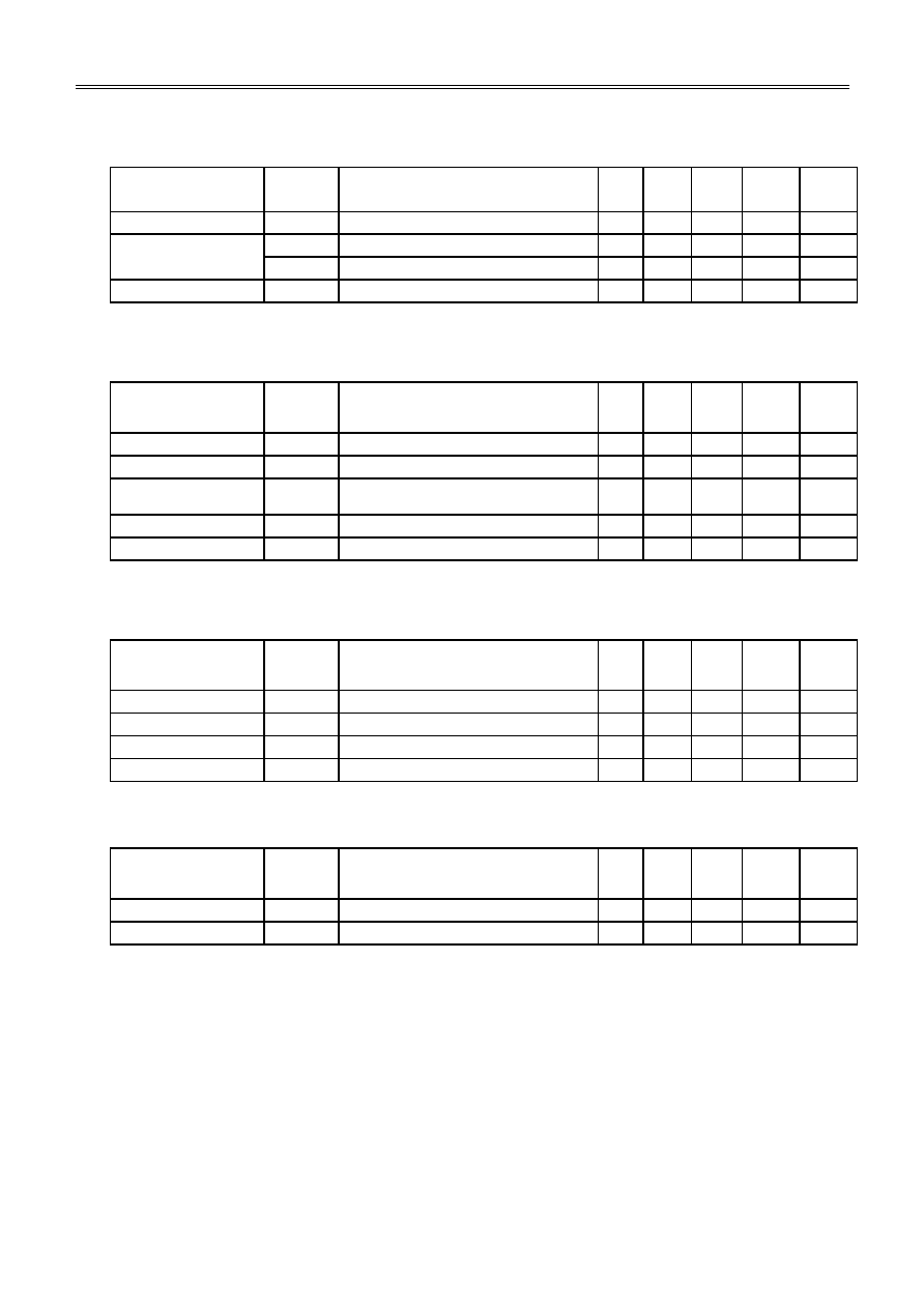
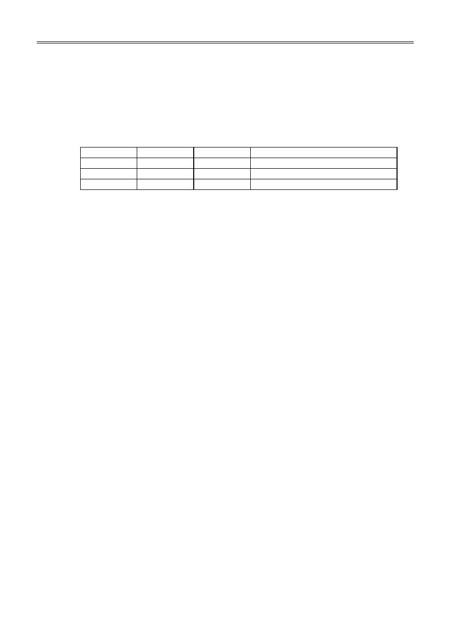
Selection Guide
1. Product name
S
-
8 3 3 5 A X X X F T
Package name (abbreviation)
Product type
240: 1/240 duty support
200: 1/200 duty support
160: 1/160 duty support
120: 1/120 duty support
2. Product list
S-8335AXXXFT Series
Bias Ratio
Common Driver Positive
Power Supply VRH
Output Voltage Range [V]
Common Driver Negative
Power Supply VRL
Output Voltage Range [V]
V
RH_min
V
RH_max
V
RL_min
V
RL_max
S-8335A240FT
8.75
8.91
16.59
-
6.87
-
12.80
S-8335A200FT
8.04
8.22
15.30
-
6.18
-
11.49
S-8335A160FT
7.33
7.48
13.93
-
5.44
-
10.13
S-8335A120FT
6.50
6.66
12.41
-
4.61
-
8.59
Note: V
RH_min
and V
RL_min
indicate the typical value of the VRH and VRL output voltage, respectively,
when the electric volume is set to the minimum, and V
RH_max
and V
RL_max
indicate the typical
value of the VRH and VRL output voltage, respectively, when the electric volume is set to the
maximum. Also, V
RH_max
is obtained from V
RETGO
◊
7.136 and V
RH_min
is obtained from V
RETGO
◊
3.832, where V
RETGO
is the regulator T output voltage.
Positive and Negative Voltage Three-channel Switching Regulator for LCD Bias Supply
S-8335 Series
Rev.5.2
Seiko Instruments Inc.
4
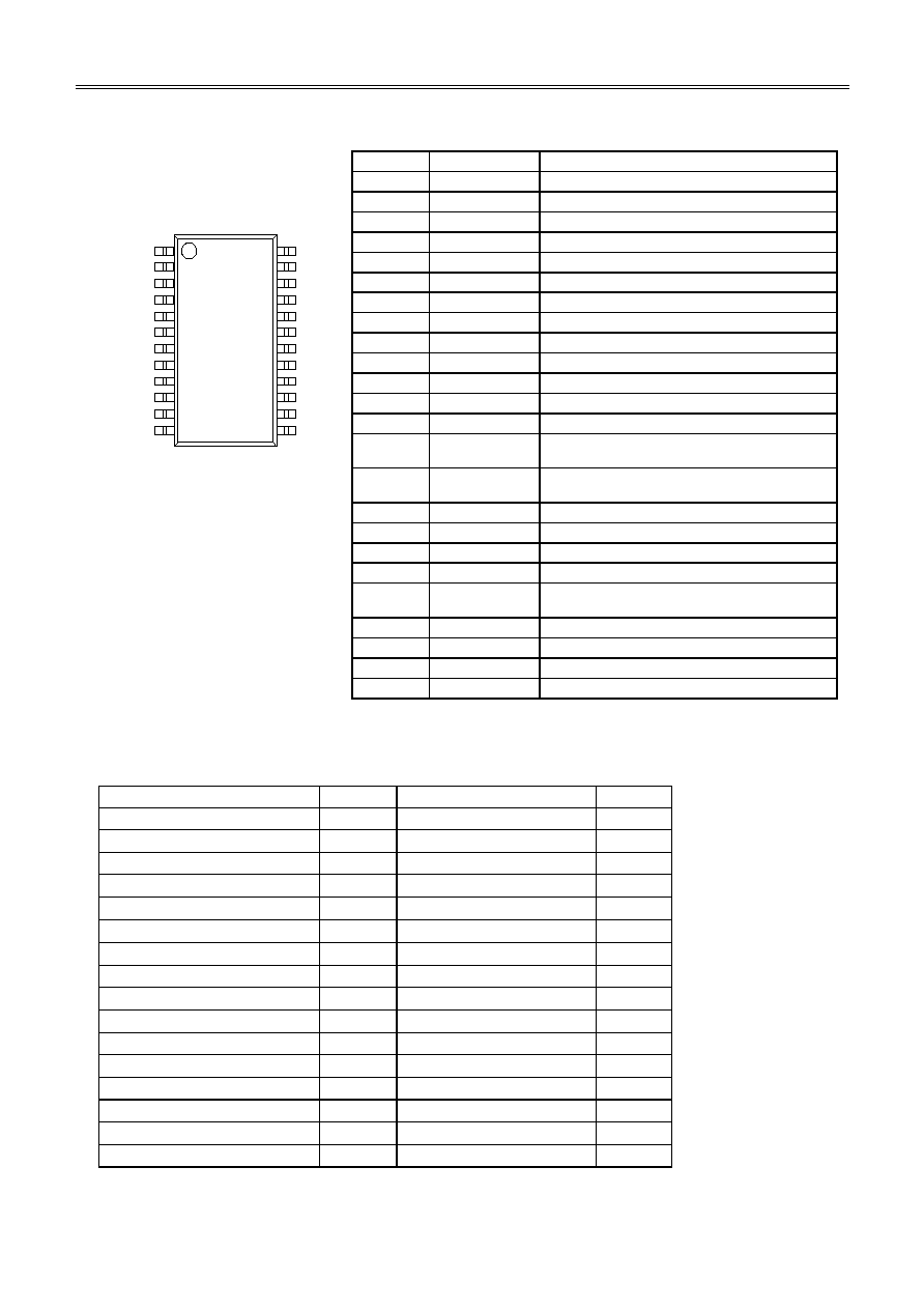
Pin Assignment
Pin No.
Pin Name
Function
1
CONT1
External inductor 1 connection pin
2
VDIN
Electric volume data input pin
3
VCLK
Electric volume clock input pin
4
VSTR_B
Electric volume strobe signal input pin
5
VSS
GND pin
6
VOUT1
Switching regulator P output voltage pin
7
CSS
Soft start capacitor connection pin
8
VREGTO
Regulator T output pin
9
VREGTF
Regulator T feedback input pin
10
VREGSO
Regulator S output pin
11
VREGSF
Regulator S feedback input pin
12
VBAT
Power supply pin
13
VYO
OP amplifier Y output pin
14
VQERR
Switching regulator Q output voltage monitoring
pin
15
EXT2
Switching regulator Q external transistor
connection pin
16
VBAT
Power supply pin
17
VSS
GND pin
18
VXO
OP amplifier X output pin
19
VDDX
OP amplifier X power supply pin
20
VREFU
Switching regulator U internal reference voltage
pin
21
VOUT3
Switching regulator U output voltage pin
22
MC2
Operating mode control pin 2
23
MC1
Operating mode control pin 1
24
CONT3
External inductor 3 connection pin
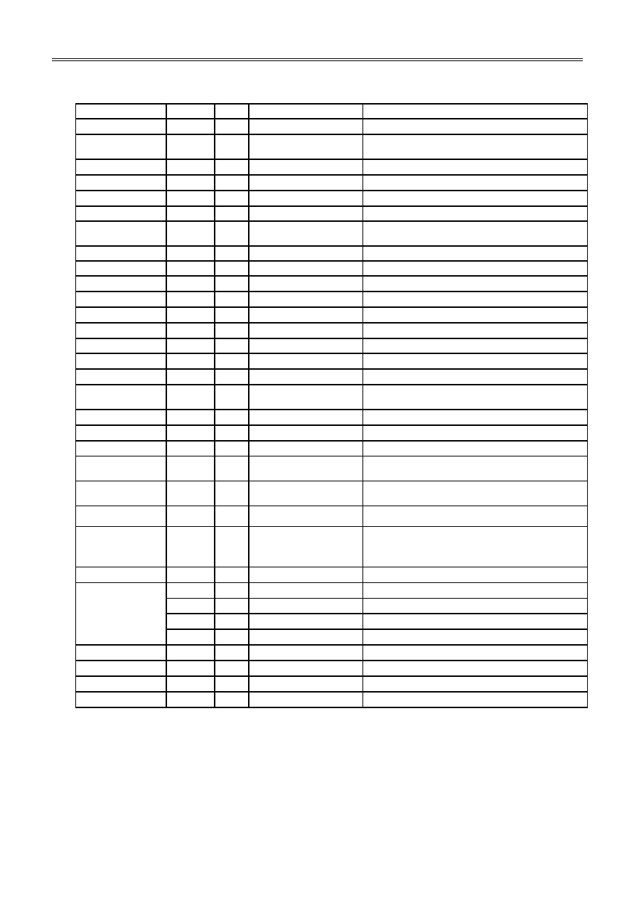
Absolute Maximum Ratings
(Unless otherwise specified: T
OPR
=25
∞
C)
Parameter
Symbol
Ratings
Unit
VBAT pin voltage
V
BAT
8
V
CONT1 pin voltage
V
CONT1
-
0.3 to +20
V
CONT1 pin current
I
CONT1
300
mA
VOUT1 pin voltage
V
OUT1
-
0.3 to +20
V
EXT2 pin voltage
V
EXT2
-
0.3 to V
BAT
+20
V
EXT2 pin current
I
EXT2
±
50
mA
CONT3 pin voltage
V
CONT3
-
0.3 to +8
V
CONT3 pin current
I
CONT3
200
mA
VOUT3 pin voltage
V
OUT3
-
0.3 to +8
V
VQERR pin voltage
V
QERR
-
0.3 to +8
V
VDDX pin voltage
V
DDX
8
V
VXO pin voltage
V
XO
-
0.3 to V
DDX
+0.3
V
Other pin voltage
-
0.3 to V
BAT
+0.3
V
Power dissipation
P
D
650
mW
Operating temperature range
T
OPR
-
20 to +70
∞
C
Storage temperature range
T
STG
-
40 to +125
∞
C
Note:
Although this IC incorporates an electrostatic protection circuit, the user is urged to avoid
subjecting the circuit to an extremely high static electricity or voltage in excess of its
performance.
24-pin TSSOP Package
Top view
1
12
24
13
Positive and Negative Voltage Three-channel Switching Regulator for LCD Bias Supply
Rev.5.2
S-8335 Series
Seiko Instruments Inc.
5
Electrical Characteristics
Note:
The data specifications are based on measured results using recommended peripheral parts (see page 9).
Common
(Unless otherwise specified: V
BA T
= 3.0 V, T
OPR
= 25
∞
C)
Item
Symbol
Conditions
Min.
Typ.
Max.
Unit
Measure-
ment
Circuit
Input voltage
V
BAT
2.4
3.0
5.0
V
-
Mode 1 current
consumption for full
oscillation
I
MC11
Current flowing from power supply pin V
BAT
.
Only regulator S and T resistance externally.
Maximum setting for electric volume. Output
voltage of DC/DC P, U, and Q are each
setting value
◊
0.9.
CONT1 and CONT3 are pulled up to 3 V via
a 300
resistor.
-
100
200
µ
A
1
Mode 1 current
consumption for
stopped oscillation
I
MC12
Current flowing from power supply pin V
BAT
.
Only regulator S and T resistance externally.
Maximum setting for electric volume. Output
voltage of DC/DC P, U, and Q are each
setting value
◊
1.2.
CONT1 and CONT3 are pulled up to 3 V via
a 300
resistor.
-
40
90
µ
A
1
Mode 2 current
consumption
I
MC2
Current flowing from power supply pin V
BAT
.
Only regulator S and T resistance externally.
Output voltage of DC/DC P, U, and Q are 0
V.
CONT1 and CONT3 are pulled up to 3 V via
a 300
resistor.
-
10
20
µ
A
1
Mode 3 current
consumption
I
MC3
Current flowing from power supply pin V
BAT
.
Only regulator S and T resistance externally.
Output voltage of DC/DC P, U, and Q are 0
V.
CONT1 and CONT3 are pulled up to 3 V via
a 300
resistor.
-
-
1.0
µ
A
1
MC1, MC2, VDIN,
VCLK, VSTR_B
V
CH
1.6
-
-
V
1
pin input voltage
V
CL
-
-
0.4
V
1
Oscillator Part
(Unless otherwise specified: V
BAT
= 3.0 V, T
OPR
= 25
∞
C)
Item
Symbol
Conditions
Min.
Typ.
Max.
Unit
Measure-
ment
Circuit
Oscillation frequency
f
OSC
80
100
120
kHz
1
Duty ratio
Duty
40
50
60
%
1

Positive and Negative Voltage Three-channel Switching Regulator for LCD Bias Supply
S-8335 Series
Rev.5.2
Seiko Instruments Inc.
6
VRH Generation Step-Up Type DC/DC P Part
(Unless otherwise specified: V
BAT
=3.0 V, T
OPR
= 25
∞
C)
Item
Symbol
Conditions
Min.
Typ.
Max.
Unit
Measure-
ment
Circuit
Output voltage 1
V
OUT11
Electric volume
at maximum,
For S-8335A240FT,
V
REGTO
= 2.325 V
16.180
16.590
17.009
V
2
I
OUT1
= 100
µ
A
For S-8335A200FT,
V
REGTO
= 2.144 V
14.918
15.300
15.683
V
For S-8335A160FT,
V
REGTO
= 1.952 V
13.582
13.930
14.278
V
For S-8335A120FT,
V
REGTO
= 1.739 V
12.098
12.410
12.718
V
Output voltage 2
V
OUT12
Electric volume
at minimum,
For S-8335A240FT,
V
REGTO
= 2.325 V
8.688
8.910
9.134
V
2
I
OUT1
= 100
µ
A
For S-8335A200FT,
V
REGTO
= 2.144 V
8.011
8.220
8.422
V
For S-8335A160FT,
V
REGTO
= 1.952 V
7.293
7.480
7.667
V
For S-8335A120FT,
V
REGTO
= 1.739 V
6.496
6.660
6.829
V
Switching
current
I
SWP
V
CONT1
= 0.4 V
60
85
-
mA
1
Switching
transistor
I
SWQP
For mode 3 (25
∞
C)
-
-
1
µ
A
1
leakage
current
For mode 3 (70
∞
C)
-
-
10
µ
A
-
VOUT1 pin input
current
I
VOUT1
For electric volume set to minimum
2
4
8
µ
A
1
VOUT1 pin sink
current
I
VOUT1L
Mode 3, V
OUT1
= 0.4 V
0.9
1.3
-
mA
1
Soft start time
T
ss
Time until the error amplifier reference
voltage reaches 90% of the final value
of the regulator T output voltage.
C
RT1
= 0.1
µ
F, C
SS
= 0.01
µ
F
10
15
35
ms
1
Efficiency
EFFIP
Electric volume set to middle, I
OUT1
=
1 mA
-
82
-
%
-

Positive and Negative Voltage Three-channel Switching Regulator for LCD Bias Supply
Rev.5.2
S-8335 Series
Seiko Instruments Inc.
7
DC/DC P Electric Volume Part
(Unless otherwise specified: V
BAT
= 3.0 V, T
OPR
= 25
∞
C)
Item
Symbol
Conditions
Min.
Typ.
Max.
Unit
Measure-
ment
Circuit
Electric volume
adjustment range
V
OUT
For S-8335A240FT, V
REGTO
= 2.325 V
8.91
±
2.5%
-
16.59
±
2.5%
V
2
For S-8335A200FT, V
REGTO
= 2.144 V
8.22
±
2.5%
-
15.30
±
2.5%
V
For S-8335A160FT, V
REGTO
= 1.952 V
7.48
±
2.5%
-
13.93
±
2.5%
V
For S-8335A120FT, V
REGTO
= 1.739 V
6.66
±
2.5%
-
12.41
±
2.5%
V
Potential division
precision
-
-
2.5
%
2
Electric volume
resolution
-
1/63
-
2
Linearity error
-
-
1/2
LSB
2
Data setup time
t
sc
5.0
-
-
µ
s
-
Data hold time
t
hc
5.0
-
-
µ
s
-
VCLK pulse width
t
dc
0.5
4.17
-
µ
s
-
VCLK period
t
tc
5.0
8.33
-
µ
s
-
VCLK
to VSTR_B
t
ss
5.0
-
-
µ
s
-
VSTR_B pulse width
t
da
5.0
-
-
µ
s
-
VSTR_B
to VCLK
t
hs
5.0
-
-
µ
s
-
D1
D0
next MSB
VDIN
VCLK
VSTR_B
t
ss
t
da
t
hs
t
sc
t
tc
t
hc
t
dc
Figure 2. Clock Timing
VDIN
VCLK
VSTR_B
State
H
-
-
Data 1
L
-
-
Data 0
-
L to H
-
Load data in shift register
-
-
L
Load shift register contents in latch
-
-
H
Hold latch data
Positive and Negative Voltage Three-channel Switching Regulator for LCD Bias Supply
S-8335 Series
Rev.5.2
Seiko Instruments Inc.
8
VRL Generation Inverter Type DC/DC Q Part
(Unless otherwise specified: V
BAT
= 3.0 V, T
OPR
= 25
∞
C)
Item
Symbol
Conditions
Min.
Typ.
Max.
Unit
Measure-
ment
Circuit
Comparator offset
V
QEROF
V
YO
= 1.45 V
-
20
0
+20
mV
1
EXT2 pin output current
I
EXT2H
For V
EXT2
= V
BAT
- 0.4 V
-
5.3
-
7.6
-
mA
1
I
EXT2L
For V
EXT2
= 0.4 V
7.4
10.5
-
mA
1
Efficiency
EFFIQ
Electric volume set to middle, I
OUT2
= 1 mA
-
60
-
%
-
Step-up Type DC/DC U Part
(Unless otherwise specified: V
BAT
= 3.0 V, T
OPR
= 25
∞
C)
Item
Symbol
Conditions
Min.
Typ.
Max.
Unit
Measure-
ment
Circuit
Output voltage
V
OUT3
For fixed V
REFU
= 2.90 V, I
OUT3
= 100
µ
A
2.97
3.05
3.12
V
2
Switching current
I
SWU
V
CONT3
= 0.4 V
73
104
-
mA
1
Switching transistor leak
current
I
SWQU
Mode 3
-
-
1.0
µ
A
1
VOUT3 pin off current
I
VOUT3L
Mode 3, V
OUT3
= 0.4 V
-
-
0.5
µ
A
1
Efficiency
EFFIU
Electric volume set to middle, I
OUT3
= 1 mA
-
95
-
%
-
OP Amplifier X Part
(Unless otherwise specified: V
BAT
= 3.0 V, T
OPR
= 25
∞
C)
Item
Symbol
Conditions
Min.
Typ.
Max.
Unit
Measure-
ment
Circuit
Output voltage
V
XO
I
OUTX
= 50
µ
A, V
REFU
= 2.90 V
2.828
2.90
2.973
V
1
Output voltage 2
V
XO2
For 1mA output
V
XO
- 0.08
-
V
XO
V
1
Current consumption
I
SSX
-
10
20
µ
A
1
VXO pin sink current
I
VXOL
Mode 3, V
XO
= 0.4 V
0.46
0.66
-
mA
1
OP Amplifier Y Part
(Unless otherwise specified: V
BAT
= 3.0 V, T
OPR
= 25
∞
C)
Item
Symbol
Conditions
Min.
Typ.
Max.
Unit
Measure-
ment
Circuit
Output voltage precision
V
YOD
= (V
XO
-V
YO
)/V
YO
, no load at Y, I
OUTX
= 50
µ
A
0.98
-
1.02
1
VYO pin sink current
I
VYOL
Mode 3, V
YO
= 0.4 V
0.46
0.66
-
mA
1

Positive and Negative Voltage Three-channel Switching Regulator for LCD Bias Supply
Rev.5.2
S-8335 Series
Seiko Instruments Inc.
9
Regulator S Part
(Unless otherwise specified: V
BAT
= 3.0 V, T
OPR
= 25
∞
C)
Item
Symbol
Conditions
Min.
Typ.
Max.
Unit
Measure-
ment
Circuit
Output voltage
V
REGSO
I
OUTS
= 50
µ
A,
RS1 = 210 k
, RS2 = 270 k
1.576
1.6
1.624
V
1
Output voltage
temperature coefficient
V
REGSO
/(V
REGSO
∑
T
OPR
)
T
OPR
= -20
∞
C to +70
∞
C (when no RS1, RS2
temperature characteristics are taken into
account)
-
±
50
-
ppm/
∞
C
-
VREGSO pin sink
current
I
VREGSOL
Mode 3, V
REGSO
= 0.4 V
0.40
0.57
-
mA
1
Regulator T Part
(Unless otherwise specified: V
BAT
= 3.0 V, T
OPR
= 25
∞
C)
Item
Symbol
Conditions
Min.
Typ.
Max.
Unit
Measure-
ment
Circuit
Output voltage
V
REGTO
For fixed V
REGSO
=
1.6 V, I
OUTT
=50
µ
A.
S-8335A240FT
2.290
2.325
2.360
V
1
For RT1, RT2
values, see Recom-
S-8335A200FT
2.112
2.14
2.176
V
mended Peripheral
Parts.
S-8335A160FT
1.923
1.95
1.981
V
S-8335A120FT
1.713
1.74
1.765
V
VREGTO pin sink current
I
VREGTOL
Mode 3, V
REGSO
=
0.4 V
0.46
0.65
-
mA
1
Positive and Negative Voltage Three-channel Switching Regulator for LCD Bias Supply
S-8335 Series
Rev.5.2
Seiko Instruments Inc.
10
Recommended Peripheral Parts (When V
ICON
=1.6 V)
Part
Value
Unit
Model No.
Remark
L1, L2, L3
150
µ
H
CDRH5D18-151
Manufactured by Sumida Electric Co., Ltd.
D1, D2, D3
MA720
Manufactured by Matsushita Electric Components Co.,
Ltd. (Schottky type)
CL1
2.2
µ
F
CM316W5R225K25A
Ceramic type
CL2
2.2
µ
F
CM316W5R225K25A
Ceramic type
CL3
10
µ
F
F930J106MA
Tantalum type
MOSFET A
2SJ356
Pch MOSFET manufactured by NEC
MOSFET F
TM5211
Pch MOSFET manufactured by Toyoda Automatic
Loom Works, Ltd.
MOSFET C
2SJ463A
Pch MOSFET manufactured by NEC
MOSFET D, E, G
2SK3019
Nch MOSFET manufactured by ROHM
CL4
1
µ
F
CM21B105K10A
Ceramic type
CL5
1
µ
F
CM21B105K10A
Ceramic type
CL6
1
µ
F
CM21B105K10A
Ceramic type
CL7
1
µ
F
CM21B105K10A
Ceramic type
CREFU
2200
pF
CM105W5R222M10A
Ceramic type
CSS
0.01
µ
F
CM105W5R103M10A
Ceramic type
CR1, CR2
0.01
µ
F
CM105W5R103K25A
Ceramic type
CRS1
-
µ
F
Ceramic type (capacitance added only when regulator S
oscillates)
CRT1
0.1
µ
F
CM105W5R104M10A
Ceramic type
CVBAT1
1
µ
F
CM105Y5V105Z10A
Ceramic type
CVBAT2
1
µ
F
CM105Y5V105Z10A
Ceramic type
CMC1, CMC2,
CMC3
0.1
µ
F
CM105Y5V104Z10A
Ceramic type
CDIN, CCLK,
CSTR_B
1
µ
F
CM105Y5V105Z10A
Ceramic type
R1, R2
1
M
±
0.5% precision
RS1
210
k
(100 + 110) k
, 100 k
replaced by thermistor.
Ishizuka Electronics Corporation thermistor 104HT (100
k
).
RS2
270
k
Use when RS1 + RS2 > 100 k
RT1
68
k
S-8335A240FT (Use when RT1 + RT2 > 185 k
)
51
k
S-8335A200FT (Use when RT1 + RT2 > 110 k
)
33
k
S-8335A160FT (Use when RT1 + RT2 > 80 k
)
13
k
S-8335A120FT (Use when RT1 + RT2 > 65 k
)
RT2
150
k
RA1
470
k
RA2
150
k
RA3
150
k
Note 1: The regulator S input (reference voltage generation circuit output) voltage has been trimmed to
0.9 V when shipped. Also, the external resistance RS1 and RS2 of the recommended
peripheral parts have been set so that V
ICON
=1.6 V. When a V
ICON
value other than 1.6 V is
used, select the resistance RS1 and RS2 values to match the V
ICON
voltage used. Also
change the RT1 and RT2 values at the same time, because the RT1 and RT2 values are
selected based on V
ICON
=1.6 V.
Note 2: CRS1 is not usually necessary. Add the capacitance only when regulator S is oscillating.
Evaluate the actual device using capacitance value on the order of 0.1
µ
F.
Note 3: The output voltage precision does not include external resistance dispersion.
Positive and Negative Voltage Three-channel Switching Regulator for LCD Bias Supply
Rev.5.2
S-8335 Series
Seiko Instruments Inc.
11
Measurement Circuits
1:
1
12
24
13
RT2
VSTR_B
VDIN
CSS
VCLK
VOUT1
RS2
CL6
CL7
CVBAT1
RT1
CRT1
RS1
CRS1
CREFU
CVBAT2
CL5
CL4
VQERR
VEXT2
VBAT VDDX
VREFU
VOUT3 MC2 MC1
2:
L1
L2
VBAT
1
12
24
13
R2
CREFU
CL2
MC2 MC1
CL6
VDIN
VREFU
CSS
VCLK VSTR_B
RT2 RS2
RT1
CRT1
RS1
CRS1
CL7
CVBAT1 CL1
R1
CR1
D1
D3
L3
CR2
PSW
D2
CVBAT2
CL5 CL4 CL3
Figure 3. Measurement Circuits

Positive and Negative Voltage Three-channel Switching Regulator for LCD Bias Supply
S-8335 Series
Rev.5.2
Seiko Instruments Inc.
12
Operation
The S-8335 Series has two step-up type and one inverter type CMOS on-chip switching regulators. These
switching regulators employ the pulse frequency modulation (PFM) method to provide low current
consumption features.
1. Operation Overview
The output of the reference voltage generation circuit is the input to regulator S. The output of regulator
S is the input to regulator T. After the extremely steep rise has been blunted by an RC low-pass filter,
the output of regulator T becomes the DC/DC P reference voltage. The DC/DC P output (pin name:
VOUT1) that is controlled by the electric volume is obtained based on this reference voltage. The
DC/DC P output becomes the common driver positive power supply (VRH).
VRH is divided by internal resistors and becomes the input of OP amplifier X. The output (pin name:
VXO) of OP amplifier X becomes the segment driver positive power supply (VCH).
Also, the input voltage of OP amplifier X becomes the reference voltage of the DC/DC U error amplifier.
The DC/DC U output (pin name: VOUT3) is obtained so that it becomes 1.05 times larger than this
reference voltage. The DC/DC U output voltage can be used for the OP amplifier X power supply
voltage.
VCH is divided by internal resistors and becomes the input of OP amplifier Y. The output (pin name:
VYO) of OP amplifier Y becomes the segment driver intermediate potential (VM).
VM becomes the reference voltage of the DC/DC Q error amplifier. DC/DC Q oscillates and VRL is
obtained so that the common driver negative power supply (VRL) and VRH are symmetric around VM.
Positive and Negative Voltage Three-channel Switching Regulator for LCD Bias Supply
Rev.5.2
S-8335 Series
Seiko Instruments Inc.
13
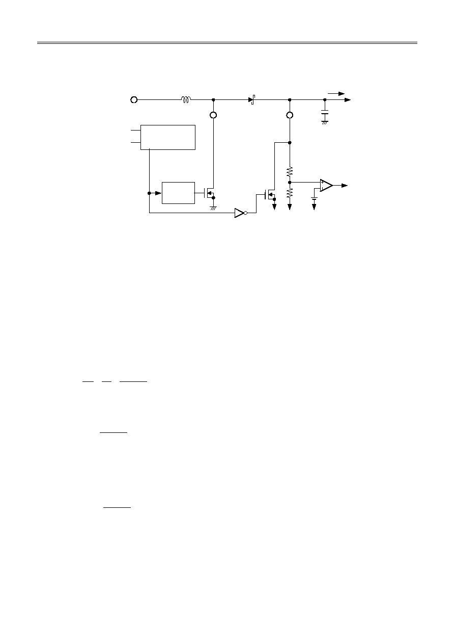
2. Step-up type switching regulators (DC/DC P and DC/DC U)
CONT
VOUT
C
OUT
D
L
A
I
OUT
V
OUT
OSC
Mode
control
MC1
MC2
M1
V
IN
R1
R2
*: In DC/DC P, R1 is a variable resistance controlled by the electric volume.
Figure 4. DC/DC P and DC/DC U
The fundamental equations {(1) to (7)} of the step-up type regulators are shown below (see Figure 4).
CONT pin voltage (V
A
) immediately after M1 is turned on (I
L
, which is the current that flows to L, is zero):
S
A
V
V
=
..........................................................................................................................
(1)
(V
S
: Unsaturated voltage of M1)
Change in I
L
with time:
L
V
V
L
V
dt
dI
S
IN
L
L
-
=
=
.....................................................................................................
(2)
Result of integrating the above equation (I
L
):
t
L
V
V
I
S
IN
L
∑
-
=
.....................................................................................................
(3)
The current I
L
flows during time t
ON
. This time (t
ON
) is determined according to the oscillation frequency
of OSC.
Peak current (I
PK
) after t
ON
:
ON
S
IN
PK
t
L
V
V
I
∑
-
=
.....................................................................................................
(4)
The energy stored in L at this time is represented by 1/2
L(I
PK
)
2
.
Next, when M1 is turned off (t
OFF
), the energy stored in L is emitted through a diode, and a counter
voltage (V
L
) is generated.

Positive and Negative Voltage Three-channel Switching Regulator for LCD Bias Supply
S-8335 Series
Rev.5.2
Seiko Instruments Inc.
14
V
L:
(
)
IN
D
OUT
L
V
V
V
V
-
+
=
.....................................................................................................
(5)
(V
D
: Diode forward voltage)
The CONT pin voltage rises by the voltage corresponding to V
OUT
+ V
D
.
Change with time of current (I
L
) that flows to V
OUT
through a diode during time t
OFF
:
L
V
V
V
L
V
dt
dI
IN
D
OUT
L
L
-
+
=
=
................................................................................................
(6)
Result of integrating the above equation:
t
L
V
V
V
I
I
IN
D
OUT
PK
L
∑
-
+
-
=
..............................................................................................
(7)
During t
ON
, the energy is stored in L and not transmitted to V
OUT
. When output current (I
OUT
) flows from
V
OUT
, the capacitor (C
OUT
) energy is used. As a result, the C
OUT
pin voltage decreases and reaches its
lowest value after time t
ON
. When M1 is turned off, the energy stored in L is transmitted through the
diode to C
OUT
, and the C
OUT
pin voltage rises dramatically. V
OUT
is a time function that indicates the
maximum value (ripple voltage: V
P-P
) when the current flowing through the diode to V
OUT
matches the
load current I
OUT
.
This ripple voltage value is calculated below.
I
OUT
when the time from immediately after t
ON
until V
OUT
reaches its highest level is set to t
1
:
1
IN
D
OUT
PK
OUT
t
L
V
V
V
I
I
∑
-
+
-
=
........................................................................................
(8)
(
)
-
+
-
=
∑
IN
D
OUT
OUT
PK
1
V
V
V
L
I
I
t
...................................................................................
(9)
Since I
L
=0 at time t
OFF
(when all inductor energy was emitted), the following is obtained from equation
(7):
PK
OFF
IN
D
OUT
I
t
V
V
V
L
=
-
+
.....................................................................................................
(10)
The following is obtained by substituting equation (10) into equation (9):
OFF
t
I
I
t
t
PK
OUT
OFF
1
∑
-
=
.....................................................................................................
(11)

Positive and Negative Voltage Three-channel Switching Regulator for LCD Bias Supply
Rev.5.2
S-8335 Series
Seiko Instruments Inc.
15
The amount of electric charge
Q
1
charged in C
OUT
during time t
1
:
2
1
IN
D
OUT
PK
t
2
1
L
V
V
V
t
I
1
∑
∑
-
+
-
=
........................................................................................
(12)
The following is obtained by substituting equation (9) into equation (12)
(
)
1
OUT
PK
1
OUT
PK
PK
1
t
2
I
I
t
I
I
2
1
I
Q
∑
∑
+
=
-
-
=
........................................................................
(13)
The voltage rise (V
P-P
) due to
Q
1
is as follows:
1
OUT
PK
OUT
OUT
1
t
2
I
I
C
1
C
Q
∑
∑
+
=
=
..............................................................................
(14)
The following is obtained when the I
OUT
consumed during time t
1
and R
ESR
, which is the Electric Series
Resistance (ESR) of C
OUT
, are taken into consideration:
OUT
1
OUT
ESR
OUT
PK
1
OUT
PK
OUT
OUT
1
C
t
I
R
2
I
I
t
2
I
I
C
1
C
Q
∑
∑
∑
∑
-
+
+
+
=
=
...................................
(15)
The following is obtained when equation (11) is substituted into equation (15):
(
)
ESR
OUT
PK
OUT
OFF
PK
2
OUT
PK
R
2
I
I
C
t
I
2
I
I
∑
∑
+
+
-
=
.................................................................
(16)
Effective ways to reduce the ripple voltage are to increase the capacitance of the capacitor connected to
the output pin and to reduce its ESR.
Note:
Although this IC has an on-chip soft-start circuit, a rush current flows because the output capacitor
(C
OUT
) and load capacitance component are charged up via the coil and diode on power application.
Therefore, care must be taken.
dt
t
L
V
V
V
dt
I
dt
I
Q
1
1
1
t
0
IN
D
OUT
t
0
PK
t
0
L
1
-
+
-
=
=
∑
∑
V
P-P
V
P-P
V
P-P
Positive and Negative Voltage Three-channel Switching Regulator for LCD Bias Supply
S-8335 Series
Rev.5.2
Seiko Instruments Inc.
16
3. Inverter type switching regulator (DC/DC Q)
The fundamental equations of the inverter type regulator are shown below.
Point A voltage immediately after M1 is turned on (I
L
, which is the current that flows to L, is zero):
S
IN
A
V
V
V
-
=
...................................
(17)
(V
S
: Unsaturated voltage of M1)
Change in I
L
with time:
L
V
V
L
V
dt
dI
S
IN
L
L
-
=
=
............................
(18)
Result of integrating the above equation (I
L
):
t
L
V
V
I
S
IN
L
∑
-
=
................................
(19)
The current I
L
flows during time t
ON
. This time (t
ON
) is determined according to the oscillation frequency
of OSC.
Peak current (I
PK
) after t
ON
:
ON
S
IN
PK
t
L
V
V
I
∑
-
=
.....................................................................................................
(20)
The energy stored in L at this time is represented by 1/2
L(I
PK
)
2
.
Next, when M1 is turned off, the energy stored in L is emitted through ground
capacitor
diode (Di),
and a counter voltage (V
L
) is generated at the same time.
V
L
:
(
)
D
OUT
L
V
V
V
+
-
=
.....................................................................................................
(21)
(V
D
: Diode forward voltage)
Change with time of current (I
L
) that flows to
-
V
OUT
through a capacitor during time t
OFF
:
L
V
V
L
V
dt
dI
D
OUT
L
L
+
=
=
.....................................................................................................
(22)
Result of integrating the above equation:
t
L
V
V
I
I
D
OUT
PK
L
∑
+
-
=
.....................................................................................................
(23)
OSC
M1
-
V
OUT
V
IN
Di
L
A
I
OUT
C
OUT
Figure 5. Inverter Type Switching Regulator

Positive and Negative Voltage Three-channel Switching Regulator for LCD Bias Supply
Rev.5.2
S-8335 Series
Seiko Instruments Inc.
17
During t
ON
, the energy is stored in L and not transmitted to
-
V
OUT
. When output current (I
OUT
) flows from
-V
OUT
, the capacitor (C
OUT
) energy is used. As a result, the C
OUT
pin voltage decreases and reaches its
lowest value after time t
ON
. When M1 is turned off, the energy stored in L is transmitted through the
diode to C
OUT
, and the C
OUT
pin voltage rises dramatically. V
OUT
is a time function that indicates the
maximum value (ripple voltage: V
P-P
) when the current flowing through the diode to V
OUT
matches the
load current I
OUT
.
This ripple voltage value is calculated below.
I
OUT
when the time from immediately after t
ON
until V
OUT
reaches its highest level is set to t
1
:
1
D
OUT
PK
OUT
t
L
V
V
I
I
∑
+
-
=
.....................................................................................................
(24)
(
)
+
-
=
∑
D
OUT
OUT
PK
1
V
V
L
I
I
t
...............................................................................................
(25)
Since I
L
=0 at time t
OFF
(when all inductor energy was emitted), the following is obtained from equation
(23):
PK
OFF
D
OUT
I
t
V
V
L
=
+
.....................................................................................................
(26)
The following is obtained by substituting equation (26) into equation (25):
OFF
t
I
I
t
t
PK
OUT
OFF
1
∑
-
=
.....................................................................................................
(27)
The amount of electric charge
Q
1
charged in C
OUT
during time t
1
:
dt
t
L
V
V
dt
I
dt
I
Q
1
1
1
t
0
D
OUT
t
0
PK
t
0
OUT
1
+
-
=
=
∑
∑
2
1
D
OUT
PK
t
2
1
L
V
V
t
I
1
∑
∑
+
-
=
.....................................................................................................
(28)
The following is obtained by substituting equation (25) into equation (28)
(
)
1
OUT
PK
1
OUT
PK
PK
1
t
2
I
I
t
I
I
2
1
I
Q
∑
∑
+
=
-
-
=
............................................................................
(29)
The voltage rise (V
P-P
) due to
Q
1
is as follows:
1
OUT
PK
OUT
OUT
1
t
2
I
I
C
1
C
Q
∑
∑
+
=
=
.................................................................................
(30)
V
P-P

Positive and Negative Voltage Three-channel Switching Regulator for LCD Bias Supply
S-8335 Series
Rev.5.2
Seiko Instruments Inc.
18
The following is obtained when the I
OUT
consumed during time t
1
is taken into consideration:
OUT
1
OUT
1
OUT
PK
OUT
OUT
1
C
t
I
t
2
I
I
C
1
C
Q
∑
∑
∑
-
+
=
=
....................................................................
(31)
The following is obtained when equation (27) is substituted into equation (31):
(
)
OUT
OFF
PK
2
OUT
PK
C
t
I
2
I
I
∑
-
=
................................................................................................
(32)
V
P-P
V
P-P
Positive and Negative Voltage Three-channel Switching Regulator for LCD Bias Supply
Rev.5.2
S-8335 Series
Seiko Instruments Inc.
19
Operation Modes and Mode Control
The mode is switched among modes 1 to 3 according to the 2-bit input from the MC1 and MC2 pins and the
MC3 signal. The MC3 signal is not an input to a pin of this IC. It is a signal required for external part control.
This signal should be supplied from the LCD driver or LCD controller.
Since the MC1 and MC2 pins are not pulled up or pulled down internally, they should not be in a floating
state. Also, note that the current consumption in standby mode may exceed 1
µ
A if there is a potential
difference between the supply voltage of MC1 and MC2 and the supply voltage of the S-8335 Series IC.
MC1
MC2
MC3*
Operation Mode
L
L
H
Mode 1 (Normal operation)
L
H
L
Mode 2 (Icon mode)
H
X
L
Mode 3 (Standby mode)
Remark: L: Low level, H: High level, X: Don't care
*
MC3 is a signal that is the input to an external switch to forcibly discharge a capacitor in modes 2 and
3.
1. Normal operation mode (MC1=L, MC2=L, MC3=H)
Step-up operation is performed.
2. Icon mode (MC1=L, MC2=H, MC3=L)
Only the reference voltage circuit and regulator S operate. The regulator S output V
REGSO
can be set
arbitrarily in the range from 1.0 to 2.2 V by using external resistors RS1 and RS2. V
REGSO
can be used
as the icon voltage. Use an RS1 value that matches the temperature characteristics of the panel by
combining a series or parallel resistor with a thermistor as necessary. See the section on regulator S for
information about the output voltage characteristics of regulator S when the output current is drawn.
3. Standby mode (MC1=H, MC3=L)
The operation of internal circuits is shut down. The current consumption does not exceed 1
µ
A.
When the MC1 pin is set high ("H" level), the operation of all internal circuits stops, and the current
consumption is dramatically reduced. At the same time, the VOUT1, VXO, VYO, VREGSO, and
VREGTO pins are each short-circuited to V
SS
by on-chip Nch transistors. (However, data that was
written to the register of the electric volume part is retained if a voltage of at least 2 V is applied between
the VBAT and VSS pins.) Since current flows at this time from the VOUT1 pin to V
SS
through a coil and
a diode at the input side, a switch for shutting down the current is required.
Figure 6 shows a sample circuit that uses NEC's 2SJ356 (Pch MOSFET) as the current breaker switch.
In this sample circuit, the small signal transistor E (Nch MOSFET) is used to turn 2SJ356 on or off by
inputting the control signal MC3 to the gate of transistor E.
An invalid current flowing to resistor RA1 during a step-up operation may affect efficiency. Resistor RA1
should be set to a high resistance value to reduce current. However, if the RA1 resistance value is set
too high, a voltage drop across resistor RA1 will occur due to the off-leak current of the small signal
transistor E, and the 2SJ356 current breaker switch may not turn off. Therefore, care must be taken.
Note:
The efficiency characteristics shown in the reference data, which were measured without a current
breaker switch, differ from the efficiency of this sample circuit.

Positive and Negative Voltage Three-channel Switching Regulator for LCD Bias Supply
S-8335 Series
Rev.5.2
Seiko Instruments Inc.
20
CONT1
RESET
MC3
RA2:
150 k
RA1:
470 k
A
E
D1
2SJ356
VOUT1
VSS
VBAT
L1
CL1
MC2
MC1
SBD
Figure 6. Sample Circuit in Which 2SJ356 is Used
When mode 3 (standby mode) is canceled, the mode returns to the one that was in effect before switching to
standby mode. For example, if the IC entered mode 3 from mode 1, it will return to mode 1 when mode 3 is
canceled.
Note 1:
If there is a potential difference between the
applied voltage to MC1 and MC2 and the
power supply voltage of the S-8335 Series, the
current consumption in standby mode may
exceed 1
µ
A.
For example, when the applied voltage to MC1
and MC2 is 3.0 V and the power supply
voltage of the S-8335 Series is 5.0 V, the
current consumption in standby mode rises to
approximately 2.5
µ
A at 25
∞
C (typ.) (see
Figure 7). The reason this occurs is that a
penetrating current flows in CMOS logic
circuits because the potential of input signals
MC1 and MC2 (3.0 V) is lower than the
internal logic power supply voltage (5.0 V).
Therefore, use this IC in such a way that no
potential difference occurs between the
applied voltage to MC1 and MC2 and the
power supply voltage of the S-8335 Series.
Note 2:
A penetrating current from V
BAT
to V
SS
flows
when the mode is switched. When MC1 (or
MC2) = "H" and MC3 = "H", a current of
approximately 6 mA flows from the VBAT pin
through the coil L1, diode D1, and transistor A
because the VOUT1 pin is short-circuited to
GND level.
0
0.5
1
1.5
2
2.5
3
2.0
2.5
3.0
3.5
4.0
4.5
5.0
V
BAT
[V]
V
MC1
= 3.0 V
St
and
by
Cur
r
ent
[
µ
A]
Figure 7. Standby Mode Current Characteristics
MC3
MC1 (or MC2)
Normal mode Standby mode Normal mode
(or icon mode)
Figure 8. Mode Switching
Positive and Negative Voltage Three-channel Switching Regulator for LCD Bias Supply
Rev.5.2
S-8335 Series
Seiko Instruments Inc.
21
Also, when MC1 (or MC2) = "L" and MC3 =
"L", VRL and GND are short-circuited via
transistor G, and a current of approximately
150 mA flows.
To reduce the penetrating current, the MC1 (or
MC2) and MC3 signals should both be
switched at the same time when modes are
switched. If this cannot be done, avoid a state
in which the MC1 (or MC2) and MC3 signals
are both low ("L" level) at the same time in
order to reduce the penetrating current (see
Figure 8).
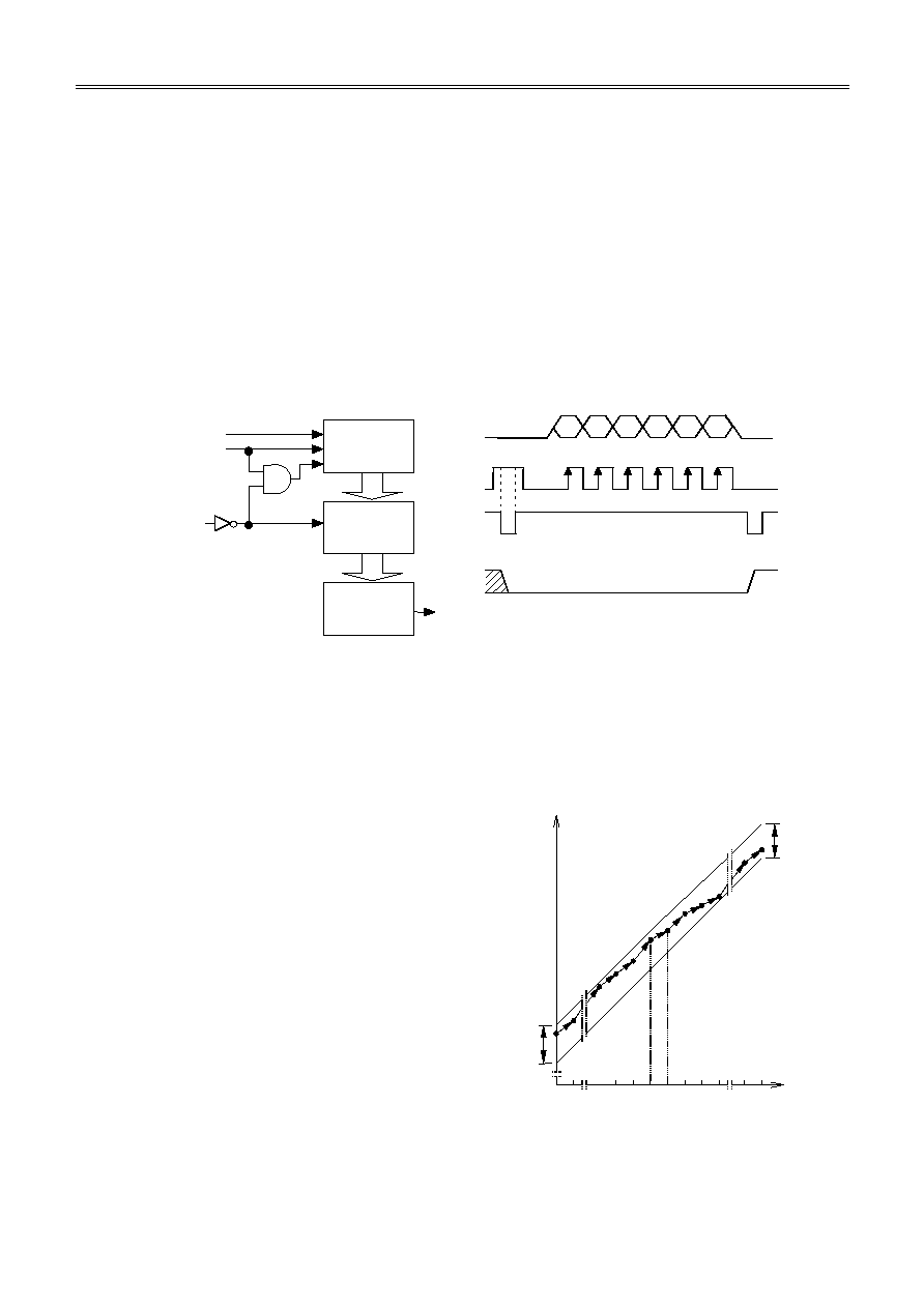
Electric volume
RESET
VCLK
VDIN
VOUT
VSTR_B
VDIN
D5
D4
D3
D2
D1
D0
(LSB)
(MSB)
VCLK
VOUT
VSTR_B
6-bit shift
register
6-bit latch
Electric
volume
Hold
Hold
Read
Reset
min. value
Setting
value
Figure 9. Block Diagram and Clock Timing of Electric Volume Part
VDIN:
This is the data input pin to the electric volume.
"Data 1" is an input for the "H" level, and "data 0" is an input for the "L" level.
(A high impedance state is prohibited.) When no data is sent, keep VDIN at the "L" level.
VCLK:
This is the clock input pin to the electric
volume.
The data of the VDIN pin is fetched to the
shift register at the clock rising edge.
When a clock with more than six bits data
is input, the data that had been read is
sequentially shifted at each clock pulse,
and the last six bits of data become
effective.
VSTR_B: This is the strobe signal input pin.
When the strobe signal goes low (set to "L"
level), the shift register contents are
fetched to the latch. The data that is
fetched to the latch is sent directly to the
electric volume, and consequently the
output voltage changes. When the strobe
signal goes high (set to "H" level), the latch
data is held.
Figure 10. Linearity Error
±
1/2 LSB
62 63
32
31
0
1
±
1/2
LSB
Electric
volume
data
(DEC)
Output
voltage
(V)
Positive and Negative Voltage Three-channel Switching Regulator for LCD Bias Supply
S-8335 Series
Rev.5.2
Seiko Instruments Inc.
22
The electric volume has 6-bit resolution. The integral and differential linearity errors are
±
0.5LSB. For
example, if you want the VRH output voltage range to vary between 8.91 and 16.59 V, you can obtain a
linearity precision of
±
61 mV by selecting the S-8335A240FT.
Since the register contents are undefined when the power is turned on, they must be reset. Even if the MC1
pin or MC2 pin is set high ("H" level) and the MC3 signal is set low ("L" level) and the step-up operation
stops, the electric volume register contents are retained if a voltage of at least 2 V is applied between the
VBAT and VSS pins. Register "WRITE" and "RESET" operations are also available in this state.
The register is initialized to "000000" and the output voltage is set to its minimum value by setting VCLK =
"H" and VSTR_B = "L".
Turn on the power with MCI = "H" and MC3 = "L". Then initialize the register contents by setting VCLK = "H"
and VSTR_B="L" and begin the step-up operation by switching the MC1 and MC2 pins low ("L" level) and
the MC3 signal high ("H" level).
Caution:
If a step-up operation is started without initializing the data in the register after turning on the
power, the maximum output voltage may appear at the VOUT pins and connected devices or
instruments may be damaged. It is recommended to connect a pull-down resistor between V
SS
and the external part pins that the MC3 signal enters and to connect a pull-up resistor between the
MC1 pin and V
BAT
.
Note:
If there is a potential difference between
the applied voltage to VDIN, VCLK, and
VSTR_B and the power supply voltage of
the S-8335 Series, the current
consumption in standby mode may exceed
1
µ
A. For example, when the applied
voltage to VDIN, VCLK, and VSTR_B is 3.0
V and the power supply voltage of the S-
8335 Series is 5.0 V, the current
consumption in standby mode rises to
approximately 2.5
µ
A at 25
∞
C (typ.) (see
Figure 11). The reason this occurs is that
a penetrating current flows in the CMOS
logic circuits because the potential of input
signals VDIN, VCLK, and VSTR_B (3.0 V)
is lower than the internal logic power
supply voltage (5.0 V). A similar situation
occurs for the power supply voltage of MC1
and MC2 (see Note in the Mode Control
section).
Figure 11. Standby Mode Current Characteristics
0
0.5
1
1.5
2
2.5
3
2.0
2.5
3.0
3.5
4.0
4.5
5.0
V
BAT
[V]
V
DIN
= 3.0 V
S
t
andb
y c
u
rr
ent
[
µ
A]

Positive and Negative Voltage Three-channel Switching Regulator for LCD Bias Supply
Rev.5.2
S-8335 Series
Seiko Instruments Inc.
23
OP amplifier X
The power supply voltage of OP amplifier X is
generated using DC/DC U so that it is approximately
1.05 times larger than the output voltage of OP
amplifier X. Since the difference between the power
supply voltage and output voltage is kept small, the
power loss is extremely small and efficiency is
increased. Figure 12 shows the output voltage of OP
amplifier X when source current is drawn.
OP amplifier Y
V
BAT
is used for the power supply voltage of OP amplifier Y. Figures 13 and 14 show the output voltage of
OP amplifier Y when source current and sink current are drawn, respectively.
Regulator S Part
V
BAT
is used for the power supply voltage of the
regulator S part. The regulator S output V
REGSO
can
be set arbitrarily in the range from 1.0 to 2.2 V by
using external resistor RS1 and RS2. V
REGSO
can be
used as the icon voltage. Use an RS1 value that
matches the temperature characteristics of the panel
by combining a series or parallel resistor with a
thermistor as necessary.
Also, CRS1 is a capacitor for preventing oscillation. It
is required only when the regulator oscillates. Adjust
the CRS1 value when the RS1 and RS2 values are
changed. Using the actual device, confirm that the
regulator does not oscillate. Figure 15 shows the
voltage V
REGSO
when current is drawn.
Figure 12. OP Amplifier X Output Voltage
0
0.5
1
1.5
2
500
1000
1500
2000
SOURCE CURRENT, I
OUTY
[
µ
A]
V
YO
[V
]
EV=MIN
EV=MID
EV=MAX
240 dot,25
∞
C
V
BAT
=3.0V
0
0.5
1
1.5
2
-
2000
-
1500
-
1000
-
500
SINK CURRENT, I
OUTY
[
µ
A]
V
YO
[V
]
EV=MIN
EV=MID
EV=MAX
240 dot,25
∞
C
V
BAT
=3.0V
Figure 13. VYO Pin Source Current Characteristics
Figure 14. VYO Pin Sink Current Characteristics
1.46
1.48
1.5
1.52
1.54
1.56
1.58
1.6
0
500
1000
1500
2000
I
OUT
[
µ
A]
V
RE
G
S
O
[V]
V
BAT
=2.4V
V
BAT
=3.0V
V
BAT
=5.0V
Figure 15. V
REGSO
Characteristics
0
0.5
1
1.5
2
2.5
3
3.5
4
500
1000
1500
2000
SOURCE CURRENT, I
OUTX
[
µ
A]
V
XO
[
V
]
EV=MIN
EV=MID
EV=MAX
240 dot,25
∞
C
V
BAT
=3.0V
Positive and Negative Voltage Three-channel Switching Regulator for LCD Bias Supply
S-8335 Series
Rev.5.2
Seiko Instruments Inc.
24
Regulator T Part
V
BAT
is used for the power supply voltage of the
regulator T part. The regulator T output V
REGTO
can
be set by using external resistance RT1 and RT2.
Set V
REGTO
to match the voltage range that is to be
used.
The common-driver voltage V
RH_max
is obtained by
V
REGTO
◊
7.136, and V
RH_min
is obtained by V
REGTO
◊
3.832. Figure 16 shows the voltage V
REGTO
when
current is drawn.
Power Supply Rising Edge Sequence
The power supply rising edge sequence is V
RH
, V
CH
, V
M
, V
RL
. The falling edge sequence is V
RL
, V
M
, V
CH
,
V
RH
. (See Figure 17.)
t
V
V
RH
V
M
V
CH
V
RL
V
RH
: 2 V/div
V
CH
: 2 V/div
V
M
: 2 V/div
V
RL
: 5 V/div
t : 5 ms/div
Figure 17. Rising and Falling Edge Sequences
Soft Start
The soft-start function blunts the rising edge of the reference voltage V
REGTO
by using an external capacitor
C
SS
and an internal resistor so that the rush current can be reduced to some degree corresponding to this
moderated ascent. However, note that this is not a complete soft start because the switching regulators of
the S-8335 Series use PFM control.
Figure 16. V
REGTO
Characteristics
2
2.05
2.1
2.15
2.2
2.25
2.3
2.35
0
500
1000
1500
2000
I
OUT
[
µ
A]
V
RE
G
T
O
[V
]
V
BAT
=2.4V
V
BAT
=3.0V
V
BAT
=5.0V
Positive and Negative Voltage Three-channel Switching Regulator for LCD Bias Supply
Rev.5.2
S-8335 Series
Seiko Instruments Inc.
25
Selection of External Parts
1. Inductor
The inductance value significantly affects the maximum output current I
OUT
and efficiency
(EFFI).
Figure 18 shows graphs of the dependency of I
OUT
and EFFI for the S-8335 Series on the inductance
value L.
Figure 18. Dependency of I
OUT
and EFFI on Inductance Value L
As the L value decreases, the peak current I
PK
increases, and I
OUT
reaches its maximum at a certain L
value. If the L value decreases further, the current driving capability of the switching transistor becomes
insufficient, and I
OUT
is reduced.
Also, as the L value increases, the power loss due to I
PK
at the switching transistor decreases, and the
efficiency reaches its maximum at a certain L value. If the L value increases further, the power loss due
to the series resistance of the coil increases, and efficiency is reduced.
The recommended inductance value is 100 to 150
µ
H for DC/DC P and 100 to 180
µ
H for DC/DC Q and
DC/DC U.
DC-DC P
(V
OUT
= 16.6 V, V
BAT
= 3.0 V)
100
150
I
OUT
EFFIP
I
OUT
EFFIP
Recommended
range
L value (
µ
H)
DC-DC Q (
V
OUT
=16.6 V, V
BAT
=3.0 V )
100
180
I
OUT
EFFIQ
I
OUT
EFFIQ
Recommended
range
L value (
µ
H)
DC-DC U (V
OUT
= 3.99 V, V
BAT
= 3.0 V )
100
180
I
OUT
EFFIU
I
OUT
EFFIU
150
Recommended
range
L value (
µ
H)

Positive and Negative Voltage Three-channel Switching Regulator for LCD Bias Supply
S-8335 Series
Rev.5.2
Seiko Instruments Inc.
26
When you select inductors, pay attention to the permissible current of the inductors. If a current that
exceeds the permissible current flows in the inductor, magnetic saturation will occur in the inductor. This
may cause a significant decrease in efficiency and may damage the IC due to excessive current.
Therefore, select inductors so that the peak current I
PK
does not exceed the permissible current. The
peak current I
PK
in non-continuous mode is given by the following equation.
)
A
(
L
f
)
V
V
V
(
I
2
I
OSC
IN
D
OUT
OUT
PK
∑
-
+
∑
=
......................................................................................
(33)
where f
OSC
is the oscillation frequency. V
D
is approximately 0.4 V.
For example, assume that output voltage V
OUT
= 16.6 V, with load current I
OUT
= 2mA, using
S-8335A240FT with the input voltage V
IN
= 3 V and f
OSC
= 100 kHz. If 150
µ
H is selected for the L value,
then I
PK
= 61 mA from equation (33). Therefore, an inductor having a permissible current of at least 61
mA at an L value of 150
µ
H should be selected.
2. Diode
An off-chip diode must satisfy the following conditions.
∑
Low forward voltage:
V
F
< 0.3 V
∑
Fast switching speed:
500 ns max.
∑
Reverse breakdown voltage: V
OUT
+V
F
or more
∑
Rated current:
I
PK
or more
3. Capacitors (CVBAT, CL)
The input capacitor (CVBAT) can improve efficiency by decreasing the power supply impedance and
stabilizing the input current. Select the capacitor value according to the impedance of the power supply
used. Connect a capacitor of at least 1
µ
F to each of the two power supply pins.
For the output capacitor (CL), use a capacitor having a small Electric Series Resistance (ESR) and large
capacitance to stabilize the ripple voltage. Standard capacitor values are at least 2.2
µ
F for CL1 and
CL2 and at least 10
µ
F for CL3. In particular, a tantalum electrolytic capacitor having excellent low
temperature characteristics and low leakage current characteristics should be used. A capacitor having
a large capacitance produces more stable output and leads to higher efficiency.
Positive and Negative Voltage Three-channel Switching Regulator for LCD Bias Supply
Rev.5.2
S-8335 Series
Seiko Instruments Inc.
27
Standard Circuits
12
1
6
2
3
24
4
21
VD
IN
VC
L
K
VSTR
_
B
VO
U
T
3
CONT
3
CONT
1
VO
U
T
1
: small current VSS,
:
large current VSS
16
5
17
23
22
10
11
8
9
7
15
13
14
20
19
18
VREGTF VREGTO
VREGSF
RT1
RT2
CRT1
CL7
CSS
F
L2
D2
CL6
CL2
G
D
C
RA3
VBAT
MC3
EXT2
VICON
VREGSO
VYO
MC2
CMC1
VBAT
MC1
CVBAT2
VQERR
VXO
VDDX
CREFU
VREFU
Electric
volume
DC/DC P
DC/DC U
DC/DC Q
op-amp X
op-amp Y
REG T
REG S
Reference
voltage
generation
circuit
Mode
control
circuit
PFM
control
circuit
Oscillator
RESET
RA2
RA1
CVBAT1
CMC2
CR1
CR2
R1
R2
VRL
VM
VCH
CL5
CL4
RS2
RS1
PFM
control
circuit
PFM
control
circuit
E
A
VRH
D3
CL1
CL3
D1
L3
L1
MC3
CRS1
Figure 19. Standard Circuits
Except for op-amp X, all of the power for the internal circuits of the S-8335 Series is supplied by the VBAT
pin.

Positive and Negative Voltage Three-channel Switching Regulator for LCD Bias Supply
S-8335 Series
Rev.5.2
Seiko Instruments Inc.
28
Pattern Diagram
In general, the switching regulator is significantly affected by the circuit board wiring. The following figure
shows a sample pattern diagram for which the effect of the circuit board wiring is small.
55 mm
59 mm
Figure 20. Pattern Diagram
Note the following points when creating a pattern diagram.
∑
There are two VSS lines (connected inside the IC).
a) VSS (pin No. 5): Large current GND
b) VSS (pin No. 17): Small current (analog) + middle current GND
∑
Arrange the VSS line and capacitors first. CVBAT, CL1, CL2, and CL3 are particularly important. Draw
the VSS line as wide as possible.
∑
Basically, make the GND part of the circuit board as broad as possible and keep the impedance low.
∑
There are two VBAT lines (not connected inside the IC).
a) VBAT (pin No. 12): Reference (low noise)
b) VBAT (pin No. 16): All others (semi-low noise)
∑
Connect CL3 at both pin No. 19 (VDDX) and pin No. 21 (VOUT3) if possible (for example, connect
6.8
µ
F at each pin).
∑
Do not use through holes at locations for connecting CL1 to CL3.
∑
Increasing CL1 makes the output more stable. If the DC/DC P output fluctuates due to ripple, and this
causes VQERR to frequently exceed the DC/DC Q error amplifier threshold value, then DC/DC Q
oscillates more than necessary and the DC/DC Q efficiency will decrease. Therefore, stabilizing the
DC/DC P output will also improve DC/DC Q efficiency.

Positive and Negative Voltage Three-channel Switching Regulator for LCD Bias Supply
Rev.5.2
S-8335 Series
Seiko Instruments Inc.
29
Application Circuit
12
1
6
2
3
24
4
21
VD
IN
VC
L
K
VSTR
_
B
VO
U
T
3
CONT
3
VBAT
CONT
1
VO
U
T
1
: small current VSS,
:
large current VSS
16
5
17
23
22
10
11
8
9
7
15
13
14
20
19
18
VREGTF VREGTO
VREGSF
RT1
RT2
CRT1
CL7
CSS
F
L2
D2
CL6
CL2
G
D
C
RA3
VBAT
MC3
EXT2
VICON
VREGSO
VYO
MC2
CMC1
VBAT
MC1
CVBAT2
MC2
MC1
VSS
VSS
VBAT
VQERR
VXO
V
DDX
CREFU
VREFU
S-8335
RA2
RA1
CVBAT1
CMC2
CR1
CR2
R1
R2
VRL
VM
VCL
VM
VCH
CL5
Common
driver
Segment
driver
CL4
RS2
RS1
A
VRH
D3
CL1
CL3
D1
L3
L1
MC3
CRS1
Figure 21. Application Circuit Example
Positive and Negative Voltage Three-channel Switching Regulator for LCD Bias Supply
S-8335 Series
Rev.5.2
Seiko Instruments Inc.
30
Precautions
∑
Mount external capacitors, diodes, coils, and other components as close as possible to the IC.
∑
The RS1, RS2, RT1, and RT2 values of the recommended peripheral parts are for V
ICON
= 1.6 V. If a
V
ICON
value other than 1.6 V is used, the resistance values should be changed. The output voltage
precision does not include external resistance dispersion.
∑
Characteristic ripple voltage and spike noise occur at the switching regulator. Since these are
significantly affected by the coil and capacitor that are used, evaluate them using actual devices when
the circuit is designed.
∑
CR1 and CR2 contribute to the stability of the VQERR pin potential and increase the efficiency of
switching regulator Q. Although a capacitance value in the range from 1000 pF to 0.01
µ
F is
recommended for CR1 and CR2, you should evaluate this value using an actual device.
∑
Make sure that the operating ambient temperature range of this IC is not exceeded due to switching
transistor power dissipation (particularly at high temperature).
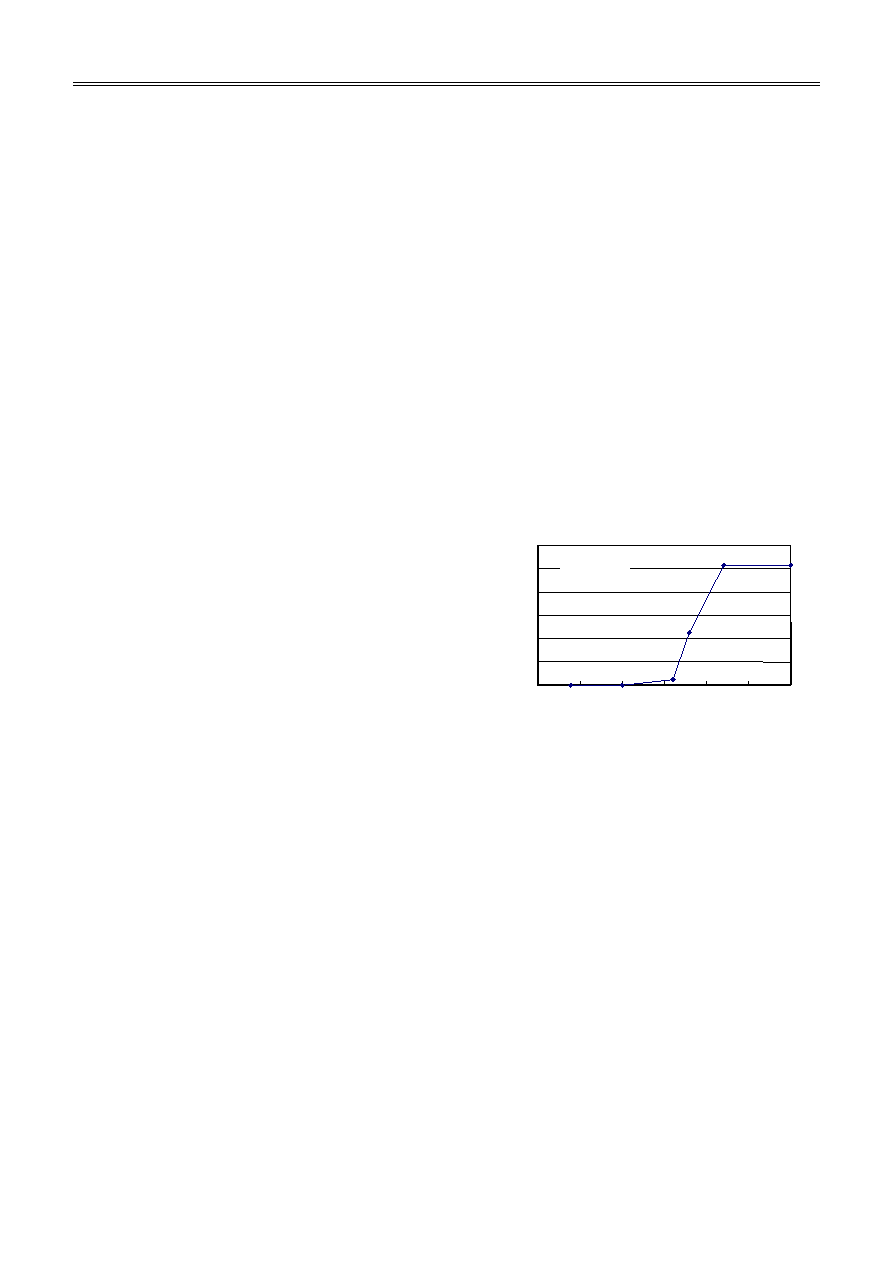
P
o
w
e
r di
s
s
i
pat
i
on P
D
(m
W
)
Ambient temperature T
OPR
(∞C)
150
100
50
0
1000
800
600
200
400
Figure 22. Power Dissipation of 24-pin TSSOP Package (Unmounted)
∑
Arrange parts so that the line to the VSS pin (indicated by the bold line in Figure 23) is as short as
possible. If this line has resistance and inductance components, the VSS potential of the IC will fluctuate
due to the switching current. If a potential difference is produced between the VSS of the CPU and the
VSS of the IC, a malfunction may occur in the interface, and the electric volume may be reset.
S-8335
CPU
CONT
VSS
VSS
VDIN
VIN
VOUT
VCLK
VSTR_B
Figure 23. VSS Line

Positive and Negative Voltage Three-channel Switching Regulator for LCD Bias Supply
Rev.5.2
S-8335 Series
Seiko Instruments Inc.
31
∑
When switching the output voltage by the electric volume, the soft start does not function. Note that an
overshoot will occur when the output voltage increases by a large amount.
∑
When the internal impedance of the power supply (VBAT) is large, the S-8335 Series may not start up.
Make sure that the internal impedance of the power supply used is sufficiently small when using this IC.
∑
Make sure that the potential of the VOUT1 pin does not exceed 20 V, which is the absolute maximum
rating, when using this IC.
∑
Make the capacitance of VDIN, VCLK, and VSTR_B large enough to prevent noise and malfunctions.
∑
Seiko Instruments Inc. shall bear no responsibility for any patent infringement by a product that includes
an IC manufactured by Seiko Instruments Inc. in relation to the method of using this IC in that product,
the product specifications, or the destination country.

Positive and Negative Voltage Three-channel Switching Regulator for LCD Bias Supply
S-8335 Series
Rev.5.2
Seiko Instruments Inc.
32
Characteristic Curves
1.
Common characteristics (Unless otherwise specified, these graphs show typical data for T
OPR
= 25∞C.)
Current consumption
Current consumption
(for mode 1 when oscillation is stopped)
(for mode 1 with full oscillation)
35
36
37
38
39
40
41
1
2
3
4
5
6
V
BAT
[V]
I
M
C12
[
µ
A]
0
20
40
60
80
100
120
140
160
1
2
3
4
5
6
V
BAT
[V]
I
M
C11
[
µ
A]
Current consumption (mode 2)
Current consumption (mode 3)
0
2
4
6
8
10
12
14
1
2
3
4
5
6
V
BAT
[V]
I
MC
2
[
µ
A]
0
0.5
1
1.5
2
2.5
3
1
2
3
4
5
6
V
BAT
[V]
I
MC
3
[
µ
A]
OP amplifier X part current consumption
VXO pin sink current
8.55
8.6
8.65
8.7
8.75
8.8
8.85
8.9
8.95
1
2
3
4
5
6
V
BAT
[V]
I
SSX
[
µ
A]
0.62
0.63
0.64
0.65
0.66
0.67
0.68
0.69
0.7
0.71
0.72
1
2
3
4
5
6
V
BAT
[V]
I
VX
O
L
[
µ
A]
VYO pin sink current
0.59
0.6
0.61
0.62
0.63
0.64
0.65
0.66
1
2
3
4
5
6
V
BAT
[V]
IV
YO
L
[
µ
A]
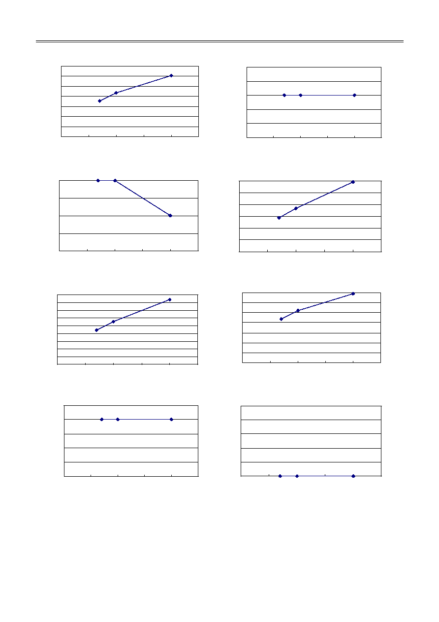
Positive and Negative Voltage Three-channel Switching Regulator for LCD Bias Supply
Rev.5.2
S-8335 Series
Seiko Instruments Inc.
33
DC/DC P part switching current
DC/DC P part switching transistor leakage current
0
20
40
60
80
100
120
140
1
2
3
4
5
6
V
BAT
[V]
I
SW
P
[m
A]
0
0.004
0.008
0.012
0.016
0.02
1
2
3
4
5
6
V
BAT
[V]
I
SW
Q
P
[
µ
A]
DC/DC Q part comparator offset voltage
EXT2 pin current (I
EXT2H
)
-
2
-
1.5
-
1
-
0.5
0
1
2
3
4
5
6
V
BAT
[V]
V
QE
R
O
F
[m
V]
0
2
4
6
8
10
12
1
2
3
4
5
6
V
BAT
[V]
I
EX
T
2
H
[m
A]
EXT2 pin current (I
EXT2L
)
DC/DC U part switching current
0
2
4
6
8
10
12
14
16
18
1
2
3
4
5
6
V
BAT
[V]
I
EX
T
2
L
[m
A]
0
20
40
60
80
100
120
140
1
2
3
4
5
6
V
BAT
[V]
I
SW
U
[m
A]
DC/DC U part switching transistor leakage current
VOUT3 pin off current
0
0.002
0.004
0.006
0.008
0.01
1
2
3
4
5
6
V
BAT
[V]
I
SW
Q
U
[
µ
A]
0
0.2
0.4
0.6
0.8
1
1
2
3
4
5
6
V
BAT
[V]
I
V
O
UT
3L
[
µ
A]
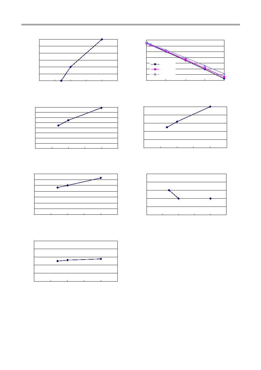
Positive and Negative Voltage Three-channel Switching Regulator for LCD Bias Supply
S-8335 Series
Rev.5.2
Seiko Instruments Inc.
34
Regulator S part output voltage (vs. V
BAT
)
Regulator S part output voltage (vs. I
OUT
)
1.597
1.5975
1.598
1.5985
1.599
1.5995
1.6
1
2
3
4
5
6
V
BAT
[V]
V
RE
G
S
O
[V]
1.46
1.48
1.5
1.52
1.54
1.56
1.58
1.6
0
500
1000
1500
2000
I
OUT
[
µ
A]
V
RE
G
S
O
[V]
V
BAT
=2.4V
V
BAT
=3.0V
V
BAT
=5.0V
VREGSO pin sink current
VREGTO pin sink current
0
0.1
0.2
0.3
0.4
0.5
0.6
0.7
0.8
1
2
3
4
5
6
V
BAT
[V]
I
VR
EG
SO
L
[m
A]
0
0.2
0.4
0.6
0.8
1
1
2
3
4
5
6
V
BAT
[V]
I
V
R
E
GTOL
[m
A]
MC1, MC2 pin high level voltage
MC1, MC2 pin low level voltage
0
0.2
0.4
0.6
0.8
1
1.2
1.4
1
2
3
4
5
6
V
BAT
[V]
V
CH
[V]
0.59
0.592
0.594
0.596
0.598
0.6
1
2
3
4
5
6
V
BAT
[V]
V
CL
[V]
Soft start time
10
12
14
16
18
20
1
2
3
4
5
6
V
BAT
[V]
t
SS
[m
s]
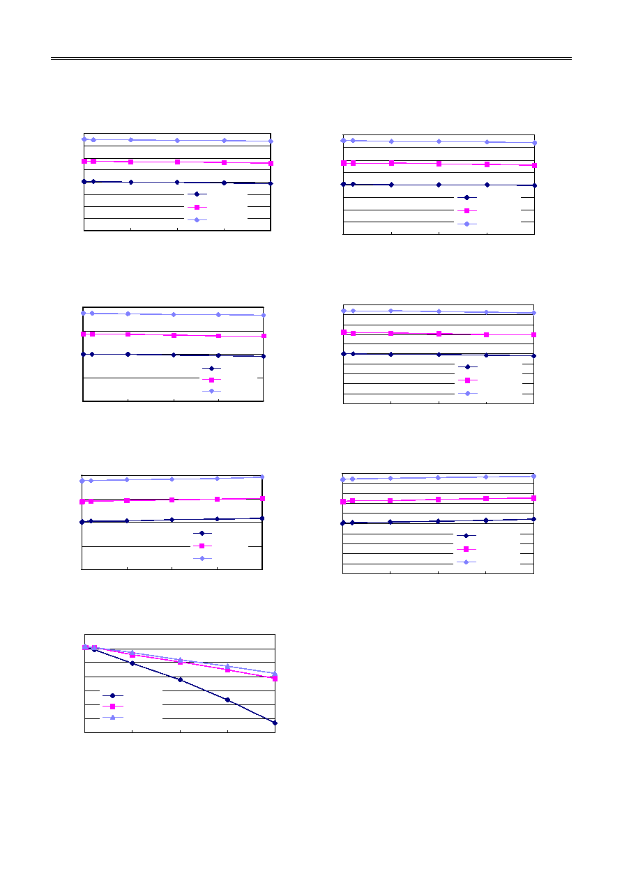
Positive and Negative Voltage Three-channel Switching Regulator for LCD Bias Supply
Rev.5.2
S-8335 Series
Seiko Instruments Inc.
35
2.
S-8335A240FT (1/240 duty. Unless otherwise specified, these graphs show typical data for T
OPR
=
25∞C.)
OP amplifier X part output voltage (V
BAT
= 2.4 V)
OP amplifier X part output voltage (V
BAT
= 3.0 V)
0
0.5
1
1.5
2
2.5
3
3.5
4
0
500
1000
1500
2000
SOURCE CURRENT, I
OUTX
[
µ
A]
V
XO
[V]
EV=MIN
EV=MID
EV=MAX
OP amplifier Y part output voltage
OP amplifier Y part output voltage
(vs. source current, V
BAT
= 2.4 V)
(vs. source current, V
BAT
= 3.0 V)
0
0.2
0.4
0.6
0.8
1
1.2
1.4
1.6
1.8
2
0
500
1000
1500
2000
SOURCE CURRENT, I
OUTY
[
µ
A]
V
YO
[V]
EV=MIN
EV=MID
EV=MAX
OP amplifier Y part output voltage
OP amplifier Y part output voltage
(vs. sink current, V
BAT
= 2.4 V)
(vs. sink current, V
BAT
= 3.0 V)
0
0.2
0.4
0.6
0.8
1
1.2
1.4
1.6
1.8
2
-
2000
-
1500
-
1000
-
500
0
SINK CURRENT, I
OUTY
[
µ
A]
V
YO
[V]
EV=MIN
EV=MID
EV=MAX
Regulator T part output voltage
2
2.05
2.1
2.15
2.2
2.25
2.3
2.35
0
500
1000
1500
2000
I
OUT
[
µ
A]
V
R
E
GTO
[V]
V
BAT
=2.4V
V
BAT
=3.0V
V
BAT
=5.0V
0
0.5
1
1.5
2
2.5
3
3.5
4
0
500
1000
1500
2000
SOURCE CURRENT, I
OUTX
[
µ
A]
V
XO
[V]
EV=MIN
EV=MID
EV=MAX
0
0.5
1
1.5
2
0
500
1000
1500
2000
SOURCE CURRENT, I
OUTY
[
µ
A]
V
YO
[V
]
EV=MIN
EV=MID
EV=MAX
0
0.5
1
1.5
2
-
2000
-
1500
-
1000
-
500
0
SINK CURRENT, I
OUTY
[
µ
A]
V
YO
[V]
EV=MIN
EV=MID
EV=MAX
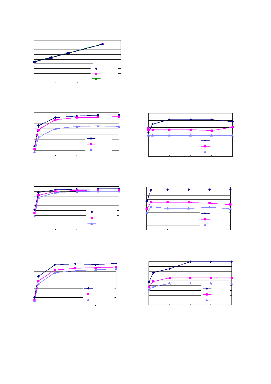
Positive and Negative Voltage Three-channel Switching Regulator for LCD Bias Supply
S-8335 Series
Rev.5.2
Seiko Instruments Inc.
36
DC/DC P part output voltage
0
2
4
6
8
10
12
14
16
18
0
20
40
60
80
EV Point
V
OU
T1
[V]
V
BAT
=2.4V
V
BAT
=3V
V
BAT
=5V
DC/DC P part output efficiency (V
BAT
= 2.4 V)
DC/DC P part output ripple voltage
(V
BAT
= 2.4 V, reference value)
0
10
20
30
40
50
60
70
80
0
500
1000
1500
2000
I
OUT
[
µ
A]
EFFIP [%
]
EV=MIN
EV=MID
EV=MAX
0
5
10
15
20
25
30
0
500
1000
1500
2000
I
OUT
[
µ
A]
Ri
ppl
e [
m
V
]
EV=MIN
EV=MID
EV=MAX
DC/DC P part output efficiency (V
BAT
= 3.0 V)
DC/DC P part output ripple voltage
(V
BAT
= 3.0 V, reference value)
0
10
20
30
40
50
60
70
80
90
0
500
1000
1500
2000
I
OUT
[
µ
A]
EFFIP[%
]
EV=MIN
EV=MID
EV=MAX
0
5
10
15
20
25
30
35
40
45
50
0
500
1000
1500
2000
I
OUT
[
µ
A]
Ri
ppl
e [
m
V
]
EV=MIN
EV=MID
EV=MAX
DC/DC P part output efficiency (V
BAT
= 5.0 V)
DC/DC P part output ripple voltage
(V
BAT
= 5.0 V, reference value)
0
20
40
60
80
100
0
500
1000
1500
2000
I
OUT
[
µ
A]
EFFIP [%
]
EV=MIN
EV=MID
EV=MAX
0
20
40
60
80
100
120
140
160
180
0
500
1000
1500
2000
I
OUT
[
µ
A]
Ri
ppl
e [
m
V
]
EV=MIN
EV=MID
EV=MAX
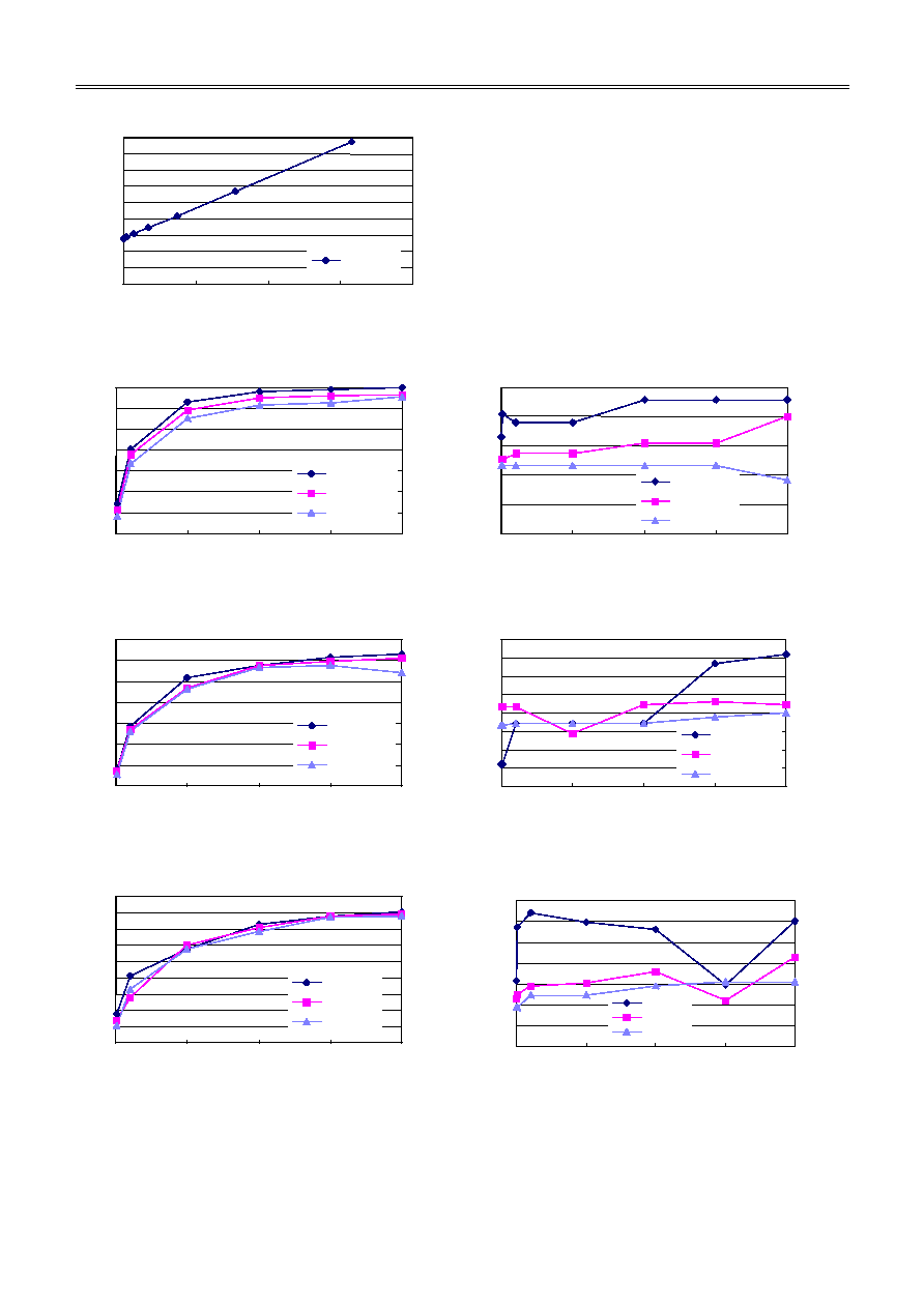
Positive and Negative Voltage Three-channel Switching Regulator for LCD Bias Supply
Rev.5.2
S-8335 Series
Seiko Instruments Inc.
37
DC/DC Q part output voltage
-13
-12
-11
-10
-9
-8
-7
-6
-5
-4
0
20
40
60
80
EV Point
V
OU
T2
[V
]
V
BAT
=3V
DC/DC Q part output efficiency (V
BAT
= 2.4 V)
DC/DC Q part output ripple voltage
(V
BAT
= 2.4 V, reference value)
0
10
20
30
40
50
60
70
0
500
1000
1500
2000
I
OUT
[
µ
A]
EFF
I
Q
[%
]
EV=MIN
EV=MID
EV=MAX
0
10
20
30
40
50
0
500
1000
1500
2000
I
OUT
[
µ
A]
Ri
ppl
e [m
V
]
EV=MIN
EV=MID
EV=MAX
DC/DC Q part output efficiency (V
BAT
= 3.0 V)
DC/DC Q part output ripple voltage
(V
BAT
= 3.0 V, reference value)
0
10
20
30
40
50
60
70
0
500
1000
1500
2000
I
OUT
[
µ
A]
EF
FIQ
[
%
]
EV=MIN
EV=MID
EV=MAX
0
10
20
30
40
50
60
70
80
0
500
1000
1500
2000
I
OUT
[
µ
A]
Ri
ppl
e [m
V
]
EV=MIN
EV=MID
EV=MAX
DC/DC Q part output efficiency (V
BAT
= 5.0 V)
DC/DC Q part output ripple voltage
(V
BAT
= 5.0 V, reference value)
0
10
20
30
40
50
60
70
80
90
0
500
1000
1500
2000
I
OUT
[
µ
A]
EFFIQ[%
]
EV=MIN
EV=MID
EV=MAX
0
50
100
150
200
250
300
350
0
500
1000
1500
2000
I
OUT
[
µ
A]
Ri
ppl
e [
m
V
]
EV=MIN
EV=MID
EV=MAX
Positive and Negative Voltage Three-channel Switching Regulator for LCD Bias Supply
S-8335 Series
Rev.5.2
Seiko Instruments Inc.
38
DC/DC U part output voltage (V
BAT
= 2.4 V)
DC/DC U part output voltage (V
BAT
= 3.0 V)
0
0.5
1
1.5
2
2.5
3
3.5
4
0
200
400
600
800
1000
I
OUTX
[
µ
A]
V
OU
T3
[V]
EV=MIN
EV=MID
EV=MAX
0
0.5
1
1.5
2
2.5
3
3.5
4
0
200
400
600
800
1000
I
OUTX
[
µ
A]
V
OU
T3
[V]
EV=MIN
EV=MID
EV=MAX
DC/DC U part output voltage (V
BAT
= 5.0 V)
DC/DC U part output voltage (EV = Min.)
0
1
2
3
4
5
0
200
400
600
800
1000
I
OUTX
[
µ
A]
V
OU
T3
[V]
EV=MIN
EV=MID
EV=MAX
0
1
2
3
4
5
0
200
400
600
800
1000
I
OUTX
[
µ
A]
V
OU
T3
[V]
V
BAT
=2.4V
V
BAT
=3V
V
BAT
=5V
DC/DC U part output voltage (EV = Mid.)
DC/DC U part output voltage (EV = Max.)
0
1
2
3
4
5
0
200
400
600
800
1000
I
OUTX
[
µ
A]
V
OU
T3
[V]
V
BAT
=2.4V
V
BAT
=3V
V
BAT
=5V
0
1
2
3
4
5
0
200
400
600
800
1000
I
OUTX
[
µ
A]
V
OU
T3
[V]
V
BAT
=2.4V
V
BAT
=3V
V
BAT
=5V
DC/DC U part output voltage (V
BAT
= 3.0 V, V
REFU
= 2.90 V)
3.04
3.045
3.05
3.055
3.06
0
20
40
60
80
EV Point
V
OU
T3
[V]
Positive and Negative Voltage Three-channel Switching Regulator for LCD Bias Supply
Rev.5.2
S-8335 Series
Seiko Instruments Inc.
39
DC/DC U part output efficiency (V
BAT
= 2.4 V)
DC/DC U part output ripple voltage
(V
BAT
= 2.4 V, reference value)
0
10
20
30
40
50
60
70
80
0
500
1000
1500
2000
I
OUT
[
µ
A]
EFFIU
[
%
]
EV=MIN
EV=MID
EV=MAX
0
2
4
6
8
10
12
14
16
0
500
1000
1500
2000
I
OUT
[
µ
A]
Ri
ppl
e [
m
V
]
EV=MIN
EV=MID
EV=MAX
DC/DC U part output efficiency (V
BAT
= 3.0 V)
DC/DC U part output ripple voltage
(V
BAT
= 3.0 V, reference value)
0
20
40
60
80
100
0
500
1000
1500
2000
I
OUT
[
µ
A]
EFFIU
[
%
]
EV=MIN
EV=MID
EV=MAX
0
5
10
15
20
25
30
35
40
0
500
1000
1500
2000
I
OUT
[
µ
A]
Ri
ppl
e [
m
V
]
EV=MIN
EV=MID
EV=MAX
DC/DC U part output efficiency (V
BAT
= 5.0 V)
DC/DC U part output ripple voltage
(V
BAT
= 5.0 V, reference value)
0
20
40
60
80
100
0
500
1000
1500
2000
I
OUT
[
µ
A]
EFFIU
[
%
]
EV=MIN
EV=MID
EV=MAX
0
0.5
1
1.5
2
2.5
3
3.5
4
0
500
1000
1500
2000
I
OUT
[
µ
A]
Ri
ppl
e [
m
V
]
EV=MIN
EV=MID
EV=MAX
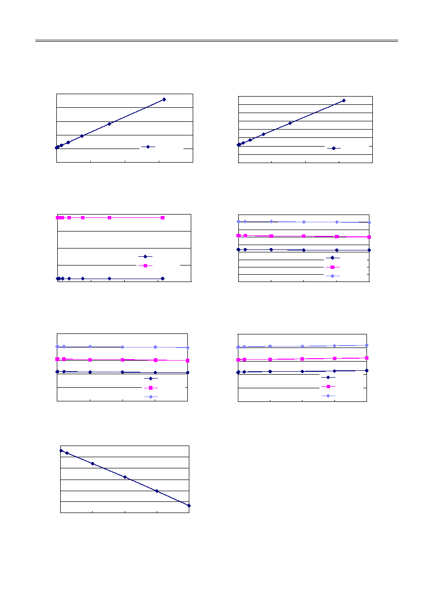
Positive and Negative Voltage Three-channel Switching Regulator for LCD Bias Supply
S-8335 Series
Rev.5.2
Seiko Instruments Inc.
40
3.
S-8335A200FT (1/200 duty. Unless otherwise specified, these graphs show typical data for T
OPR
=
25∞C.)
DC/DC P part output voltage
DC/DC Q part output voltage
6
8
10
12
14
16
0
20
40
60
80
EV Point
V
OU
T1
[V]
V
BAT
=3V
-12
-11
-10
-9
-8
-7
-6
-5
-4
0
20
40
60
80
EV Point
V
OU
T2
[V]
V
BAT
=3V
DC/DC U part output voltage (V
REFU
= 2.91 V)
OP amplifier X part output voltage
(vs. source current, V
BAT
= 3.0 V)
3
3.5
4
4.5
5
0
20
40
60
80
V
REFU
=2.91V
EV Point
V
OU
T3
[V]
V
BAT
=3V
V
BAT
=5V
0
0.5
1
1.5
2
2.5
3
3.5
4
4.5
0
500
1000
1500
2000
SOURCE CURRENT, I
OUTX
[
µ
A]
V
XO
[V]
EV=MIN
EV=MID
EV=MAX
OP amplifier Y part output voltage
OP amplifier Y part output voltage
(vs. source current, V
BAT
= 3.0 V)
(vs. sink current, V
BAT
= 3.0 V)
0
0.5
1
1.5
2
2.5
0
500
1000
1500
2000
SOURCE CURRENT, I
OUTY
[
µ
A]
V
YO
[V]
EV=MIN
EV=MID
EV=MAX
0
0.5
1
1.5
2
2.5
-
2000
-
1500
-
1000
-
500
0
SINK CURRENT, I
OUTY
[
µ
A]
V
YO
[V]
EV=MIN
EV=MID
EV=MAX
Regulator T part output voltage (V
BAT
= 3.0 V)
2
2.02
2.04
2.06
2.08
2.1
2.12
0
500
1000
1500
2000
I
OUT
[
µ
A]
V
R
E
GTO
[V]
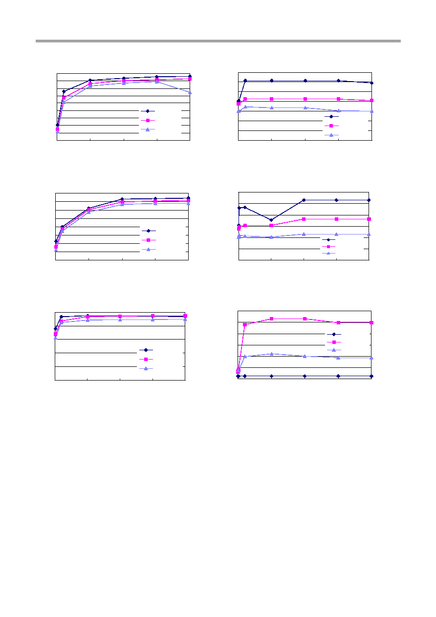
Positive and Negative Voltage Three-channel Switching Regulator for LCD Bias Supply
Rev.5.2
S-8335 Series
Seiko Instruments Inc.
41
DC/DC P part output efficiency (V
BAT
= 3.0 V)
DC/DC P part output ripple voltage
(V
BAT
= 3.0 V, reference value)
0
10
20
30
40
50
60
70
80
90
0
500
1000
1500
2000
I
OUT
[
µ
A]
EFFIP [%
]
EV=MIN
EV=MID
EV=MAX
0
10
20
30
40
50
60
70
0
500
1000
1500
2000
I
OUT
[
µ
A]
Ri
ppl
e [
m
V
]
EV=MIN
EV=MID
EV=MAX
DC/DC Q part output efficiency (V
BAT
= 3.0 V)
DC/DC Q part output ripple voltage
(V
BAT
= 3.0 V, reference value)
0
10
20
30
40
50
60
70
80
0
500
1000
1500
2000
I
OUT
[
µ
A]
EFFIQ [%
]
EV=MIN
EV=MID
EV=MAX
0
20
40
60
80
100
120
0
500
1000
1500
2000
I
OUT
[
µ
A]
Ri
ppl
e [
m
V
]
EV=MIN
EV=MID
EV=MAX
DC/DC U part output efficiency (V
BAT
= 3.0 V)
DC/DC U part output ripple voltage
(V
BAT
= 3.0 V, reference value)
0
20
40
60
80
100
0
500
1000
1500
2000
I
OUT
[
µ
A]
EFFIU
[
%
]
EV=MIN
EV=MID
EV=MAX
0
10
20
30
40
50
60
0
500
1000
1500
2000
I
OUT
[
µ
A]
Ri
ppl
e [
m
V
]
EV=MIN
EV=MID
EV=MAX
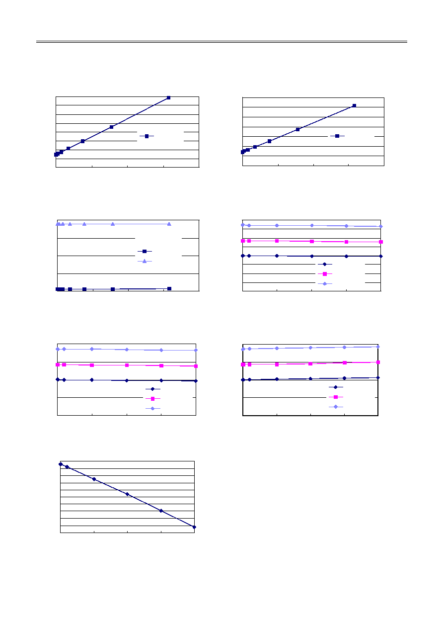
Positive and Negative Voltage Three-channel Switching Regulator for LCD Bias Supply
S-8335 Series
Rev.5.2
Seiko Instruments Inc.
42
4.
S-8335A160FT (1/160 duty. Unless otherwise specified, these graphs show typical data for T
OPR
=
25∞C.)
DC/DC P part output voltage
DC/DC Q part output voltage
6
7
8
9
10
11
12
13
14
0
20
40
60
80
EV Point
V
OU
T1
[V]
V
BAT
=3V
-11
-10
-9
-8
-7
-6
-5
-4
0
20
40
60
80
EV Point
V
OU
T2
[V]
V
BAT
=3V
DC/DC U part output voltage (V
REFU
= 2.906 V)
OP amplifier X part output voltage
(vs. source current, V
BAT
= 3.0 V)
3
3.5
4
4.5
5
0
20
40
60
80
EV Point
V
OU
T3
[V]
V
BAT
=3V
V
BAT
=5V
V
REFU
=2.906V
0
0.5
1
1.5
2
2.5
3
3.5
4
0
500
1000
1500
2000
SOURCE CURRENT, I
OUTX
[
µ
A]
V
XO
[V]
EV=MIN
EV=MID
EV=MAX
OP amplifier Y part output voltage
OP amplifier Y part output voltage
(vs. source current, V
BAT
= 3.0 V)
(vs. sink current, V
BAT
= 3.0 V)
0
0.5
1
1.5
2
0
500
1000
1500
2000
SOURCE CURRENT, I
OUTY
[
µ
A]
V
YO
[V]
EV=MIN
EV=MID
EV=MAX
0
0.5
1
1.5
2
-
2000
-
1500
-
1000
-
500
0
SINK CURRENT, I
OUTX
[
µ
A]
V
YO
[V]
EV=MIN
EV=MID
EV=MAX
Regulator T part output voltage (V
BAT
= 3.0 V)
1.83
1.84
1.85
1.86
1.87
1.88
1.89
1.9
1.91
1.92
1.93
0
500
1000
1500
2000
I
OUT
[
µ
A]
V
R
E
GTO
[V]
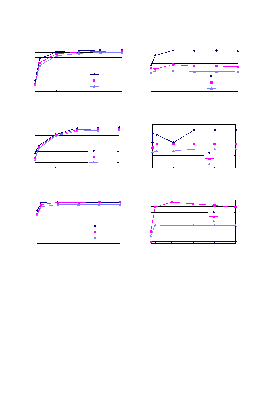
Positive and Negative Voltage Three-channel Switching Regulator for LCD Bias Supply
Rev.5.2
S-8335 Series
Seiko Instruments Inc.
43
DC/DC P part output efficiency (V
BAT
= 3.0 V)
DC/DC P part output ripple voltage
(V
BAT
= 3.0 V, reference value)
0
10
20
30
40
50
60
70
80
90
0
500
1000
1500
2000
I
OUT
[
µ
A]
EFFIP[%
]
EV=MIN
EV=MID
EV=MAX
0
10
20
30
40
50
60
70
80
0
500
1000
1500
2000
I
OUT
[
µ
A]
Ri
ppl
e [
m
V
]
EV=MIN
EV=MID
EV=MAX
DC/DC Q part output efficiency (V
BAT
= 3.0 V)
DC/DC Q part output ripple voltage
(V
BAT
= 3.0 V, reference value)
0
10
20
30
40
50
60
70
80
0
500
1000
1500
2000
I
OUT
[
µ
A]
EFFIQ[%
]
EV=MIN
EV=MID
EV=MAX
0
20
40
60
80
100
120
140
0
500
1000
1500
2000
I
OUT
[
µ
A]
Ri
ppl
e [
m
V
]
EV=MIN
EV=MID
EV=MAX
DC/DC U part output efficiency (V
BAT
= 3.0 V)
DC/DC U part output ripple voltage
(V
BAT
= 3.0 V, reference value)
0
20
40
60
80
100
0
500
1000
1500
2000
I
OUT
[
µ
A]
EFFIU
[%
]
EV=MIN
EV=MID
EV=MAX
0
5
10
15
20
25
30
35
0
500
1000
1500
2000
I
OUT
[
µ
A]
Ri
ppl
e [
m
V
]
EV=MIN
EV=MID
EV=MAX

Positive and Negative Voltage Three-channel Switching Regulator for LCD Bias Supply
S-8335 Series
Rev.5.2
Seiko Instruments Inc.
44
5.
S-8335A120FT (1/120 duty. Unless otherwise specified, these graphs show typical data for T
OPR
=
25∞C.)
DC/DC P part output voltage
DC/DC Q part output voltage
6
7
8
9
10
11
12
13
0
20
40
60
80
EV Point
V
OU
T1
[V]
V
BAT
=3V
-10
-9
-8
-7
-6
-5
-4
0
20
40
60
80
EV Point
V
OU
T2
[V]
V
BAT
=3V
DC/DC U part output voltage (V
REFU
= 2.92 V)
OP amplifier X part output voltage
(vs. source current, V
BAT
= 3.0 V)
3
3.5
4
4.5
5
0
20
40
60
80
EV Point
V
OU
T3
[V]
V
BAT
=3V
V
BAT
=5V
0
0.5
1
1.5
2
2.5
3
3.5
4
0
500
1000
1500
2000
SOURCE CURRENT, I
OUTX
[
µ
A]
V
XO
[V]
EV=MIN
EV=MID
EV=MAX
OP amplifier Y part output voltage
OP amplifier Y part output voltage
(vs. source current, V
BAT
= 3.0 V)
(vs. sink current, V
BAT
= 3.0 V)
0
0.5
1
1.5
2
0
500
1000
1500
2000
SOURCE CURRENT, I
OUTY
[
µ
A]
V
YO
[V]
EV=MIN
EV=MID
EV=MAX
0
0.5
1
1.5
2
-
2000
-
1500
-
1000
-
500
0
SINK CURRENT, I
OUTY
[
µ
A]
V
YO
[V]
EV=MIN
EV=MID
EV=MAX
Regulator T part output voltage (V
BAT
= 3.0 V)
1.64
1.65
1.66
1.67
1.68
1.69
1.7
1.71
1.72
1.73
0
500
1000
1500
2000
I
OUT
[
µ
A]
V
R
E
GTO
[V]
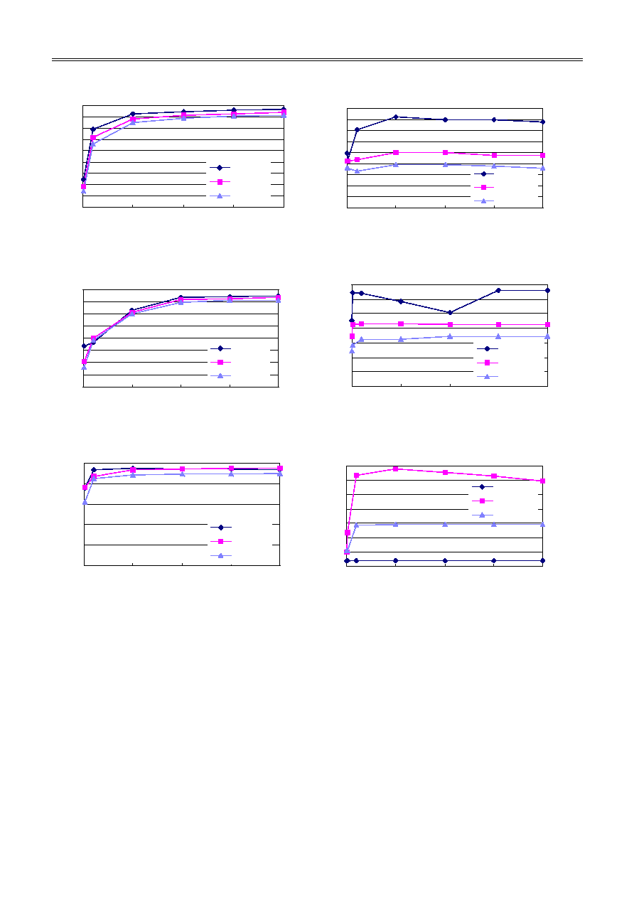
Positive and Negative Voltage Three-channel Switching Regulator for LCD Bias Supply
Rev.5.2
S-8335 Series
Seiko Instruments Inc.
45
DC/DC P part output efficiency (V
BAT
= 3.0 V)
DC/DC P part output ripple voltage
(V
BAT
= 3.0 V, reference value)
0
10
20
30
40
50
60
70
80
90
0
500
1000
1500
2000
I
OUT
[
µ
A]
EFFIP[%
]
EV=MIN
EV=MID
EV=MAX
0
10
20
30
40
50
60
70
80
90
0
500
1000
1500
2000
I
OUT
[
µ
A]
Ri
ppl
e [
m
V
]
EV=MIN
EV=MID
EV=MAX
DC/DC Q part output efficiency (V
BAT
= 3.0 V)
DC/DC Q part output ripple voltage
(V
BAT
= 3.0 V, reference value)
0
10
20
30
40
50
60
70
80
0
500
1000
1500
2000
I
OUT
[
µ
A]
EFFIQ [%
]
EV=MIN
EV=MID
EV=MAX
0
20
40
60
80
100
120
140
0
500
1000
1500
2000
I
OUT
[
µ
A]
Ri
ppl
e [
m
V
]
EV=MIN
EV=MID
EV=MAX
DC/DC U part output efficiency (V
BAT
= 3.0 V)
DC/DC U part output ripple voltage
(V
BAT
= 3.0 V, reference value)
0
20
40
60
80
100
0
500
1000
1500
2000
I
OUT
[
µ
A]
EFFIU
[
%
]
EV=MIN
EV=MID
EV=MAX
0
5
10
15
20
25
30
35
0
500
1000
1500
2000
I
OUT
[
µ
A]
Ri
ppl
e [
m
V
]
EV=MIN
EV=MID
EV=MAX
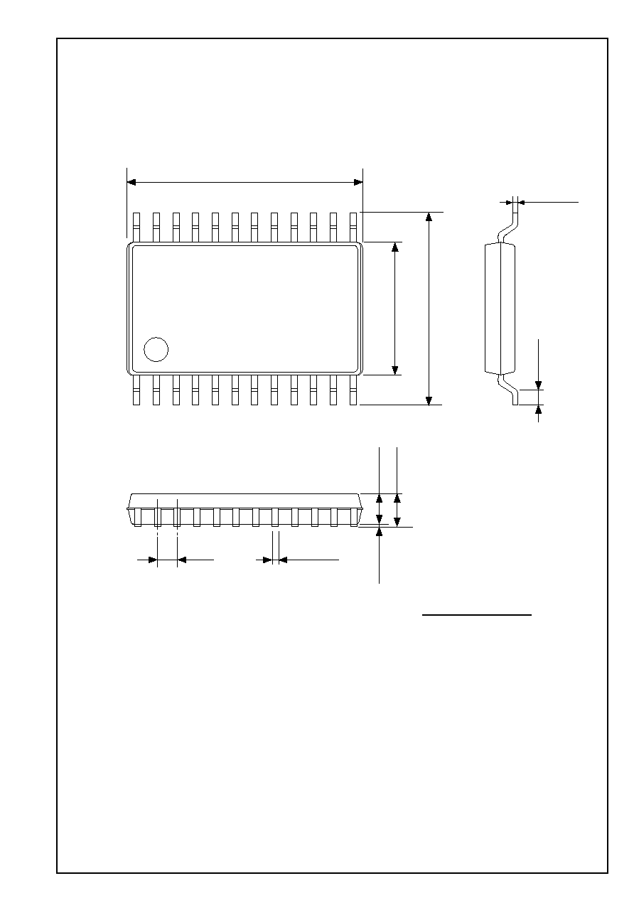
0.22±0.1
0 to 0.10
1.0±0.05
1.1 max
0.65
7.8±0.3
24
13
1
12
6.4±0.2
4.4
0.5±0.1
0.17±0.05
No.:FT024-A-P-SD-1.0
FT024-A 000214
n 24-pin TSSOP
Unit:mm
lDimensions

∑
The information described herein is subject to change without notice.
∑
Seiko Instruments Inc. is not responsible for any problems caused by circuits or diagrams described herein
whose related industrial properties, patents, or other rights belong to third parties. The application circuit
examples explain typical applications of the products, and do not guarantee the success of any specific
mass-production design.
∑
When the products described herein are regulated products subject to the Wassenaar Arrangement or other
agreements, they may not be exported without authorization from the appropriate governmental authority.
∑
Use of the information described herein for other purposes and/or reproduction or copying without the
express permission of Seiko Instruments Inc. is strictly prohibited.
∑
The products described herein cannot be used as part of any device or equipment affecting the human
body, such as exercise equipment, medical equipment, security systems, gas equipment, or any apparatus
installed in airplanes and other vehicles, without prior written permission of Seiko Instruments Inc.
∑
Although Seiko Instruments Inc. exerts the greatest possible effort to ensure high quality and reliability, the
failure or malfunction of semiconductor products may occur. The user of these products should therefore
give thorough consideration to safety design, including redundancy, fire-prevention measures, and
malfunction prevention, to prevent any accidents, fires, or community damage that may ensue.