Document Outline
- S-8337/8338 Series
- Cover
- Features
- Applications
- Packages
- Block Diagram
- Product Code Structure
- Pin Assignment
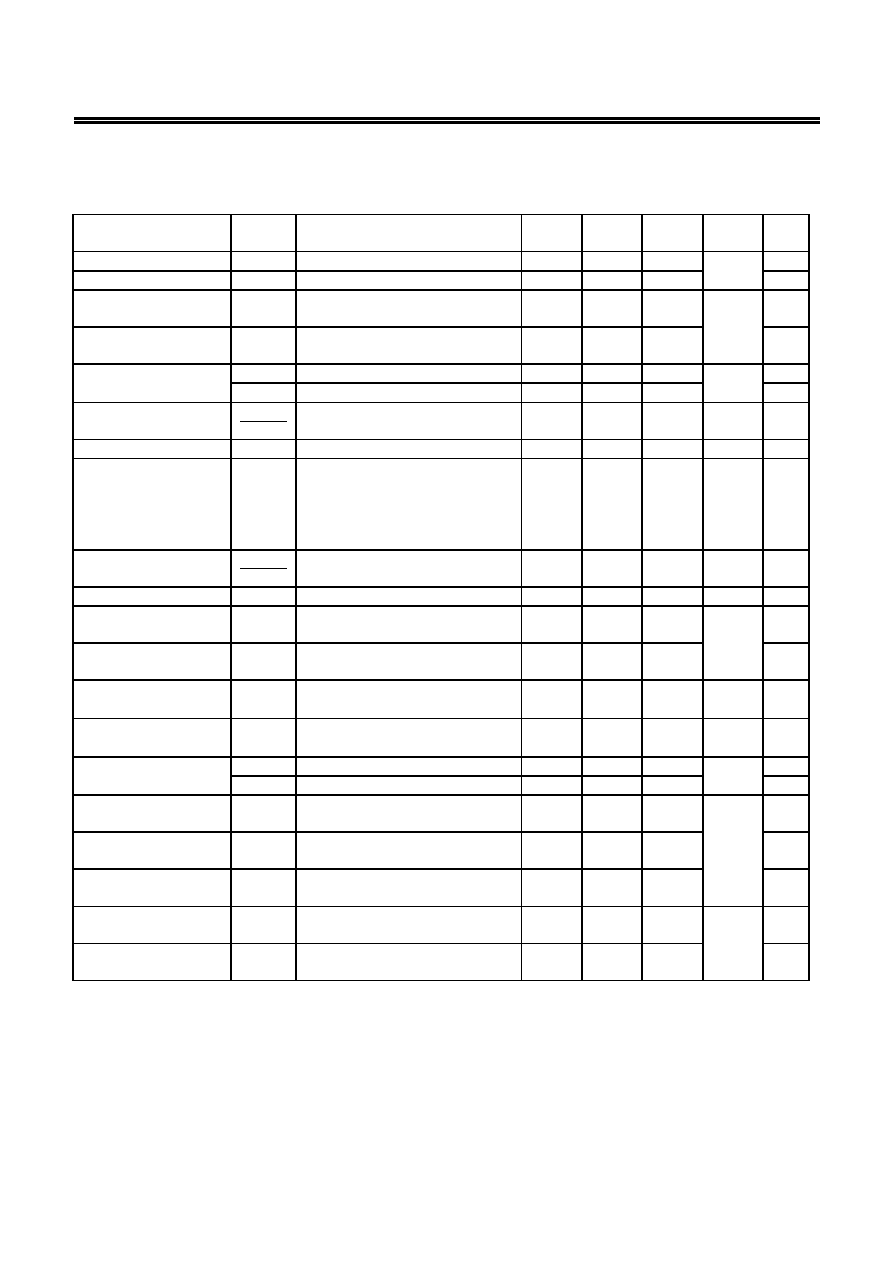
- Absolute Maximum Ratings
- Electrical Characteristics
- External Parts When Measuring Electrical Characteristics
- Test Circuit Diagram
- Operation
- External Parts Selection
- Standard Circuits
- Power Dissipation of Package
- Precaution
- Example of Major Temperature Characteristics (Ta =-40 to 85įC)
- Example of Major Power Supply Dependence Characteristics (Ta =25įC)
- Example of External Parts Dependence Characteristics
- Examples of Transient Response Characteristics
- Reference Data
- Marking Specification
- Package drawing
Rev.2.0
_00
STEP-UP, HIGH-FREQUENCY, PWM CONTROL
SWITCHING REGULATOR CONTROLLERS
S-8337/8338 Series
Seiko Instruments Inc.
1
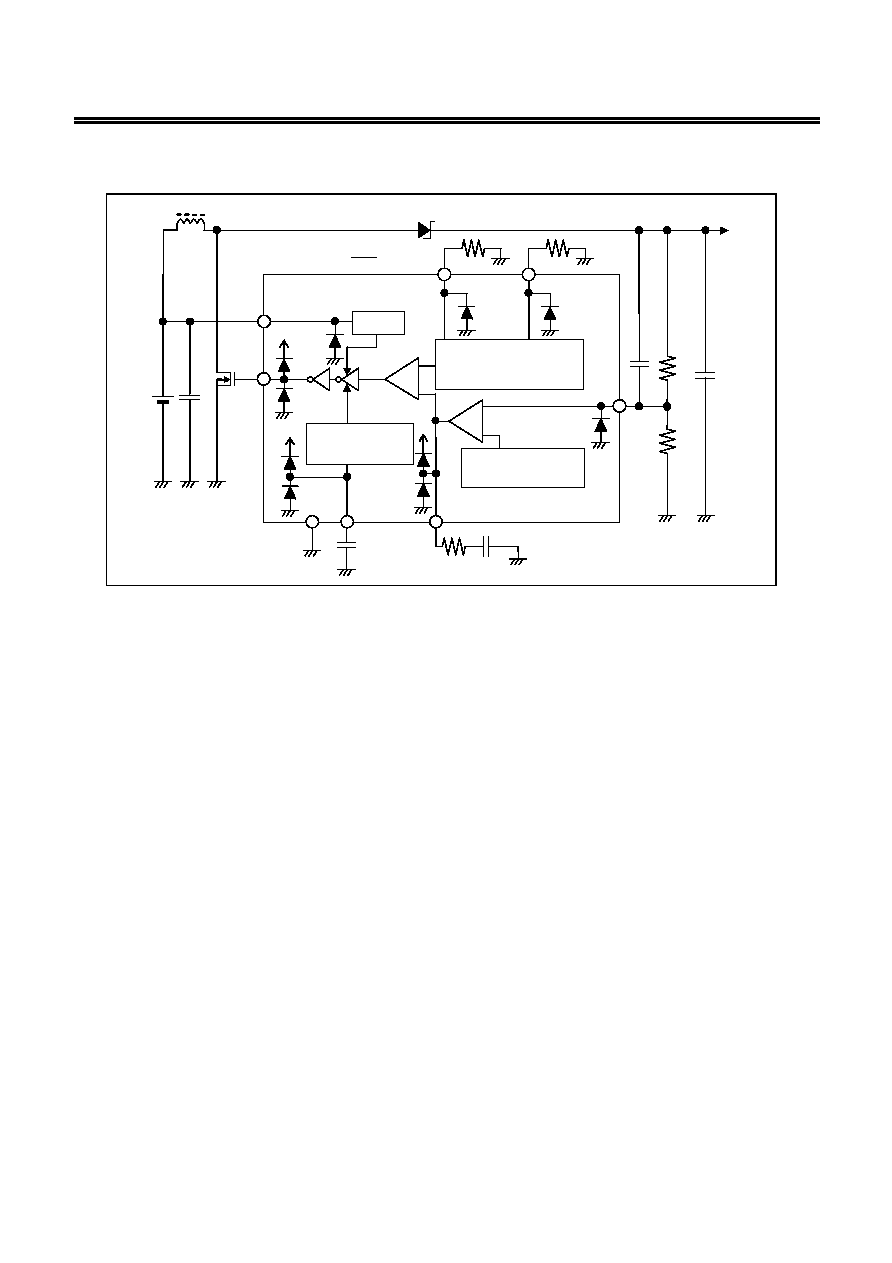
The S-8337/8338 Series is a CMOS step-up switching regulator which mainly
consists of a reference voltage circuit, an oscillator, an error amplifier, a PWM
controller, an under voltage lockout circuit (UVLO), and a timer latch short-circuit
protection circuit. Because its minimum operating voltage is as low as 1.8 V, this
switching regulator is ideal for the power supply of an LCD or for portable
systems that operate on a low voltage. The internal oscillation frequency can be
set up to 1.133 MHz, via the resistor connected to the ROSC pin.
With the S-8337 Series, the maximum duty ratio of PWM control can be
controlled by the resistor connected to the RDuty pin. With the S-8338 Series,
the maximum duty ratio is fixed (to 88%). The phase compensation and gain
value can be adjusted according to the values of the resistor and capacitor
connected to the CC pin. Therefore, the operation stability and transient
response can be correctly set for each application. The reference voltage
accuracy is as high as 1.0 V
Ī1.5%, and any voltage can be output by using an
external output voltage setting resistor.
In addition, the delay time of the short-circuit protection circuit can be set by
using the capacitor connected to the CSP pin. If the maximum duty condition
continues because of short-circuiting, the capacitor externally connected to the
CSP pin is charged, and oscillation stops after a specific time. This condition is
cleared by re-application of power or by setting the switching regulator (S-8338
Series) to the shutdown status. A ceramic capacitor or a tantalum capacitor is
used as the output capacitor, depending on the setting. This controller IC allows
various settings and selections and employs a small package, making it very
easy to use.
Features
∑ Low voltage operation:
1.8 V to 6.0 V
∑ Oscillation frequency:
286 kHz to 1.133 MHz (selectable by external resistor)
∑ Maximum duty:
47 to 88.5% (selectable by external resistor) (S-8337 Series)
Fixed to 88% typ. (S-8338 Series)
∑ Reference voltage:
1.0 V
Ī1.5%
∑
UVLO (under-voltage lockout) function:
Detection voltage can be selected from between 1.5 V and 2.3 V in 0.1 V steps.
Hysteresis width can be selected from between 0.1 V and 0.3 V in 0.1 V steps.
∑ Timer latch short-circuit protection circuit:
Delay time can be set using an external capacitor.
∑ Soft-start function:
Soft-start time can be selected in three steps, 10 ms, 15 ms, and 20 ms.
∑ Phase compensation external setting:
Adjustable by connecting resistor and capacitor in series to GND.
∑ Shutdown function:
S-8338 Series, shutdown current consumption: 1.0
ĶA max.
∑ Small package:
8-pin SON(A), 8-pin TSSOP
Applications
∑ Power supplies for LCDs and CCDs
∑ Power supplies for portable equipment
Packages
Drawing code
Package name
Package Tape Reel
8-Pin SON(A)
PN008-A
PN008-A
PN008-A
8-Pin TSSOP
FT008-A
FT008-E
FT008-E
STEP-UP, HIGH-FREQUENCY, PWM CONTROL SWITCHING REGULATOR CONTROLLERS
S-8337/8338 Series
Rev.2.0
_00
2
Seiko Instruments Inc.
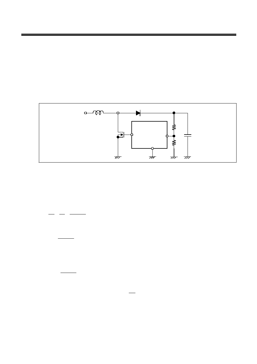
Block Diagram
PWM
comparator
V
OUT
Timer latch
short-circuit
protection circuit
RDuty (S-8337) or
ON/OFF (S-8338)
RFB2
VSS
RFB1
FB
SD
L
VIN
EXT
UVLO
CSP
CC
RZ
CZ
ROSC
M1
CFB
+
-
+
-
Oscillator
Maximum duty circuit
Reference voltage
(1.0 V) soft-start
circuit
Error amplifier
C
IN
C
L
Figure 1 Block Diagram

STEP-UP, HIGH-FREQUENCY, PWM CONTROL SWITCHING REGULATOR CONTROLLERS
Rev.2.0
_00
S-8337/8338 Series
Seiko Instruments Inc.
3
Product Code Structure
1. Product name
S-833
x A x x x -
xxxx
Indicates package type and packing
specification of IC.
P8T1: 8-Pin SON(A)
T8T1: 8-Pin TSSOP
Soft-start time setting
A: 10 ms
B: 15 ms
C: 20 ms
UVLO setting
A: 2.3 V
B: 2.2 V
C: 2.1 V
D: 2.0 V
E: 1.9 V
F: 1.8 V
G:
1.7 V
H:
1.6 V
I: 1.5 V
UVLO hysteresis setting
A: 0.1 V
B: 0.2 V
C: 0.3 V
Pin setting
7: With MaxDuty setting function
8: With Shutdown function
STEP-UP, HIGH-FREQUENCY, PWM CONTROL SWITCHING REGULATOR CONTROLLERS
S-8337/8338 Series
Rev.2.0
_00
4
Seiko Instruments Inc.
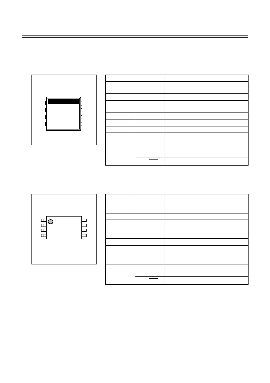
Pin Assignment
Table 1
Pin No.
Pin Name
Functions
1 CC
Error amplifier circuit output phase
compensation pin
2
FB
Output voltage feedback pin
3 CSP
Short-circuit protection delay time
setting pin
4
VIN
Power supply input pin
5
EXT
External transistor connection pin
6 VSS
GND
pin
8-Pin SON(A)
Top view
1
3
2
4
8
6
7
5
7 ROSC
Oscillation frequency setting resistor
connection pin
Figure 2
8 RDuty
Maximum duty setting resistor
connection pin (S-8337 Series)
OFF
ON/
Shutdown pin (S-8338 Series)
Table 2
Pin No.
Pin Name
Functions
1 CC
Error amplifier circuit output phase
compensation pin
2
FB
Output voltage feedback pin
3 CSP
Short-circuit protection delay time
setting pin
4
VIN
Power supply input pin
5
EXT
External transistor connection pin
6 VSS
GND
pin
8-Pin TSSOP
Top view
1
3
2
4
8
6
7
5
7 ROSC
Oscillation frequency setting resistor
connection pin
Figure 3
8 RDuty
Maximum duty setting resistor
connection pin (S-8337 Series)
OFF
ON/
Shutdown pin (S-8338 Series)
STEP-UP, HIGH-FREQUENCY, PWM CONTROL SWITCHING REGULATOR CONTROLLERS
Rev.2.0
_00
S-8337/8338 Series
Seiko Instruments Inc.
5
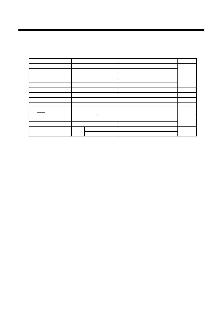
Absolute Maximum Ratings
Table 3 Absolute Maximum Ratings
(Unless otherwise specified: Ta
= 25įC, V
SS
= 0 V)
Parameter Symbol
Ratings Unit
VIN pin voltage
V
IN
V
SS
≠ 0.3 to V
SS
+ 6.5
V
FB pin voltage
V
FB
V
SS
≠ 0.3 to V
SS
+ 6.5
EXT pin voltage
V
EXT
V
SS
≠ 0.3 to V
IN
+ 0.3
CSP pin voltage
V
CSP
V
SS
≠ 0.3 to V
IN
+ 0.3
CC pin voltage
V
CC
V
SS
≠ 0.3 to V
IN
+ 0.3
CC pin current
I
CC
Ī10
mA
ROSC pin voltage
V
ROSC
V
SS
≠ 0.3 to V
IN
+ 0.3
V
ROSC pin current
I
ROSC
Ī10
mA
RDuty pin voltage
V
RDuty
V
SS
≠ 0.3 to V
IN
+ 0.3
V
RDuty pin current
I
RDuty
Ī10
mA
ON/OFF pin voltage
V
ON/OFF
V
SS
≠ 0.3 to V
SS
+ 6.5
V
Operating temperature
T
opr
≠40 to
+85
įC
Storage temperature
T
stg
≠40 to
+125
8-Pin SON(A)
300
mW
Power dissipation
P
D
8-Pin TSSOP
300
Caution The absolute maximum ratings are rated values exceeding which the product
could suffer physical damage. These values must therefore not be exceeded
under any conditions.

STEP-UP, HIGH-FREQUENCY, PWM CONTROL SWITCHING REGULATOR CONTROLLERS
S-8337/8338 Series
Rev.2.0
_00
6
Seiko Instruments Inc.
Electrical Characteristics
1. S-8337 Series
Table 4 Electrical Characteristics
(Unless otherwise specified: V
IN
= 3.3 V, Ta = 25įC)
Parameter Symbol
Conditions
Min.
Typ.
Max.
Unit
Test
Circuit
Operating input voltage
V
IN
1.8
6.0
2
FB voltage
V
FB
0.985
1.000
1.015
V
2
Current consumption
I
SS1
f
osc
= 700 kHz
V
FB
= 0.95 V
400 700 ĶA 1
I
EXTH
V
EXT
= V
IN
- 0.4 V
-100
-60 1
EXT pin output current
I
EXTL
V
EXT
= 0.4 V
100
160
mA
1
FB voltage temperature
coefficient
V
FB
Ta
Ta
= -40įC to +85įC
Ī100
ppm/įC 2
FB pin input current
I
FB
-0.1
+0.1
ĶA 1
Oscillation frequency
*1
f
osc
f
osc
= 1133 kHz (R
OSC
= 120 k)
f
osc
= 700 kHz (R
OSC
= 200 k)
f
osc
= 286 kHz (R
OSC
= 510 k)
V
FB
= 0.9 V
Waveform on EXT pin is measured.
f
osc
◊ 0.9
f
osc
f
osc
◊ 1.1
kHz 1
Oscillation frequency
temperature coefficient
f
osc
Ta
Ta
= -40įC to +85įC
f
osc
= 700 kHz
1000 ppm/įC 1
Max. duty
*2
MaxDuty
f
osc
= 700 kHz (R
OSC
= 200 k)
MaxDuty
= 88.5% (R
Duty
= 100 k)
MaxDuty
= 77% (R
Duty
= 300 k)
MaxDuty
= 47% (R
Duty
= 820 k)
MaxDuty
- 5
MaxDuty
MaxDuty
+ 5
% 1
Soft-start time
t
SS
t
SS
= 10 ms, 15 ms, 20 ms
Selected in three steps
t
SS
◊ 0.75
t
SS
t
SS
◊ 1.5
1
Short-circuit protection
delay time
*3
t
PRO
t
PRO
= 50 ms
(CSP
= 0.1 ĶF)
37.5 50 75
ms
1
UVLO detection voltage V
UVLO
V
UVLO
= 1.5 V to 2.3 V
Selected in 0.1 V steps
V
UVLO
◊ 0.95
V
UVLO
V
UVLO
◊ 1.05
V 1
UVLO hysteresis width V
UVLOHYS
V
UVLOHYS
= 0.1 V to 0.3 V
Selected in 0.1 V steps
V
UVLOHYS
◊ 0.6
V
UVLOHYS
V
UVLOHYS
◊ 1.4
mV 1
I
CCH
V
FB
= 2 V
-75
-50
-37.5 1
CC pin output current
I
CCL
V
FB
= 0 V
37.5
50
75
ĶA
1
Timer latch reset voltage
V
RTLT
0.7
1.0
1.3
V
1
*1. The recommended range of the resistance (R
osc
) for setting the oscillation frequency is R
osc
= 120 k to 510 k (f
OSC
= 286 kHz to
1.133 MHz). However, the oscillation frequency is in the range of typical values when an ideal resistor is externally connected, so
actually the fluctuation of the IC (
Ī10%) must be considered.
*2. The recommended range of the resistance (R
Duty
/R
osc
) for setting the maximum duty is R
Duty
/R
osc
= 0.5 to 4.1 (MaxDuty = 47 to 88.5%).
However, the maximum duty is in the range of typical values when an ideal resistor is externally connected, so actually the fluctuation
of the IC (
Ī5%) must be considered.
*3. The short-circuit protection time can be set by the external capacitor, and the maximum set value by the external capacitor is unlimited
when an ideal case is assumed. But, use C
SP
= approximately 0.47 ĶF as a target maximum value due to the need to consider the
discharge time of the capacitor.
STEP-UP, HIGH-FREQUENCY, PWM CONTROL SWITCHING REGULATOR CONTROLLERS
Rev.2.0
_00
S-8337/8338 Series
Seiko Instruments Inc.
7
2. S-8338 Series
Table 5 Electrical Characteristics
(Unless otherwise specified: V
IN
= 3.3 V, Ta = 25įC)
Parameter Symbol
Conditions
Min.
Typ.
Max.
Unit
Test
Circuit
Operating input voltage
V
IN
1.8
6.0
2
FB voltage
V
FB
0.985
1.000
1.015
V
2
Current consumption
I
SS1
f
osc
= 700 kHz
V
FB
= 0.95 V
400 700
1
Shutdown current
consumption
I
SSS
V
IN
= 6.0 V
1.0
ĶA
1
I
EXTH
V
EXT
= V
IN
- 0.4 V
-100
-60 1
EXT pin output current
I
EXTL
V
EXT
= 0.4 V
100
160
mA
1
FB voltage temperature
coefficient
V
FB
Ta
Ta
= -40įC to +85įC
Ī100
ppm/įC 2
FB pin input current
I
FB
-0.1
+0.1
ĶA 1
Oscillation frequency
*1
f
osc
f
osc
= 1133 kHz (R
OSC
= 120 k)
f
osc
= 700 kHz (R
OSC
= 200 k)
f
osc
= 286 kHz (R
OSC
= 510 k)
V
FB
= 0.9 V
Waveform on EXT pin is measured
f
osc
◊ 0.9
f
osc
f
osc
◊ 1.1
kHz 1
Oscillation frequency
temperature coefficient
f
osc
Ta
Ta
= -40įC to +85įC
f
osc
= 700 kHz
1000 ppm/įC 1
Max. duty ratio
MaxDuty f
osc
= 700 kHz (R
OSC
= 200 k) 83 88 93 %
1
Soft-start time
t
SS
t
SS
= 10 ms, 15 ms, 20 ms
Selectable in three steps
t
SS
◊ 0.75
t
SS
t
SS
◊ 1. 5
1
Short-circuit protection
delay time
*2
t
PRO
t
PRO
= 50 ms
(CSP
= 0.1 ĶF)
37.5 50 75
ms
1
UVLO detection voltage
V
UVLO
V
UVLO
= 1.5 V to 2.3 V
Selected in 0.1 V steps
V
UVLO
◊ 0.95
V
UVLO
V
UVLO
◊ 1.05
V 1
UVLO hysteresis width V
UVLOHYS
V
UVLOHYS
= 0.1 V to 0.3 V
Selected in 0.1 V steps
V
UVLOHYS
◊ 0.6
V
UVLOHYS
V
UVLOHYS
◊ 1.4
mV 1
I
CCH
V
FB
= 2 V
-75
-50
-37.5 1
CC pin output current
I
CCL
V
FB
= 0 V
37.5
50
75
ĶA
1
Timer latch reset
voltage
V
RTLT
0.7
1.0
1.3
1
Shutdown pin input
voltage (High level)
V
SH
1.8
1
Shutdown pin input
voltage (Low level)
V
SL
0.3
V
1
Shutdown pin input
current (High level)
I
SH
-0.1
+0.1 1
Shutdown pin input
current (Low level)
I
SL
-0.1
+0.1
ĶA
1
*1. The recommended range of the resistance (R
osc
) for setting the oscillation frequency is R
osc
= 120 k to 510 k (f
osc
= 286 kHz to 1.133
MHz). However, the oscillation frequency is in the range of typical values when an ideal resistor is externally connected, so actually
the fluctuation of the IC (
Ī10%) must be considered.
*2. The short-circuit protection time can be set by the external capacitor, and the maximum set value by the external capacitor is unlimited
when an ideal case is assumed. But, use C
SP
= approximately 0.47 ĶF as a target maximum value due to the need to consider the
discharge time of the capacitor.

STEP-UP, HIGH-FREQUENCY, PWM CONTROL SWITCHING REGULATOR CONTROLLERS
S-8337/8338 Series
Rev.2.0
_00
8
Seiko Instruments Inc.
External Parts When Measuring Electrical Characteristics
Table 6 External Parts
Element Name
Symbol
Manufacturer
Part Number
Inductor L
TDK
Corporation
LDR655312T 4.7
ĶH
Diode SD
Rohm
Co.,
Ltd.
RB491D
Output capacitor
CL
Ceramic 10
ĶF
Transistor M1
Sanyo Electric Co., Ltd. MCH3406
Oscillation frequency setting resistor
ROSC
200
k
(when f
OSC
= 700 kHz)
Maximum duty ratio setting resistor
RDuty
300 k
(when MaxDuty = 77%)
Short-circuit protection delay time
setting capacitor
CSP
0.1
ĶF (when t
PRO
= 50 ms)
Output voltage setting resistor 1
RFB1
8.2
k
(when V
OUT
= 9.2 V)
Output voltage setting resistor 2
RFB2
1.0
k
(when V
OUT
= 9.2 V)
FB pin capacitor
CFB
180 pF
Phase compensation resistor
RZ
200
k
Phase compensation capacitor
CZ
0.01
ĶF
STEP-UP, HIGH-FREQUENCY, PWM CONTROL SWITCHING REGULATOR CONTROLLERS
Rev.2.0
_00
S-8337/8338 Series
Seiko Instruments Inc.
9
Test Circuit Diagram
1.
CC
EXT
VSS
FB
CSP
ROSC
VIN
A
RDuty
(ON/OFF)
CSP
CIN
CZ
RZ
ROSC RDuty
Oscilloscope
Figure 4
2.
CC
EXT
VSS
FB
CSP
ROSC
VIN
V
RDuty
(ON/OFF)
CSP
CIN
M1
CL
RFB2
RFB1 CFB
RZ
CZ
L
SD
ROSC RDuty
Figure 5
STEP-UP, HIGH-FREQUENCY, PWM CONTROL SWITCHING REGULATOR CONTROLLERS
S-8337/8338 Series
Rev.2.0
_00
10
Seiko Instruments Inc.
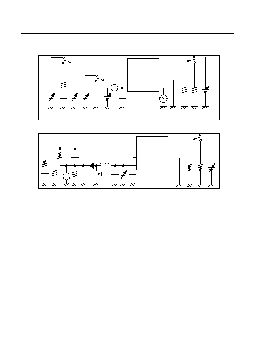
Operation
1. Switching control method
PWM control (S-8337/8338 Series)
The S-8337/8338 Series is a DC-DC converter using a pulse width modulation method (PWM).
The pulse width of the S-8337/8338 Series varies from 0% to the maximum duty set by RDuty
depending on the load current (the pulse width of the S-8338 Series is fixed to 88%), but its switching
frequency does not change. Consequently, the ripple voltage generated from switching can be
removed easily via a filter.
2. Soft-start function
For this IC, the built-in soft-start circuit controls the rush current and overshoot of the output voltage
when powering on or when the
OFF
ON/
pin is switched to the "H" level. A reference voltage
adjustment method is adopted as the soft-start method. The following describes the soft-start
function.
The raising of the output voltage is controlled by slowly raising the reference voltage of the error
amplifier input from 0 V at power on as shown in Figure 6. The soft-start function is realized by
controlling the voltage of the FB pin so that it is the same potential as the reference voltage that is
slowly raised. A Rail-to-Rail amplifier is adopted as the error amplifier, which means that the voltage
is loop controlled so that it can be the same as the reference voltage.
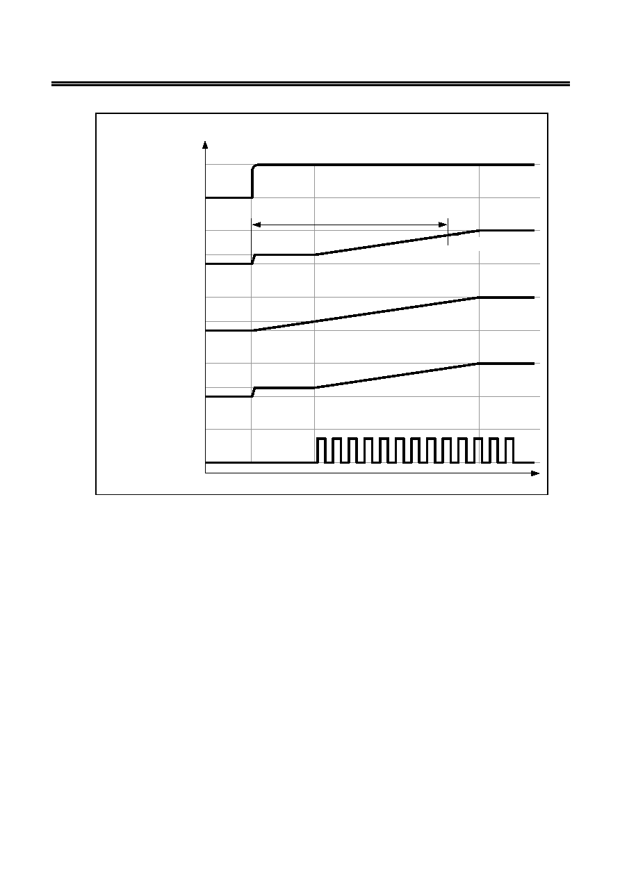
The following explains the operation at power on (refer to Figure 7).
When V
IN
is raised from 0 V to 3.3 V, the V
OUT
voltage rises to a value close to V
IN
via the inductor L
and diode SD. This raises the voltage of the FB pin (V
FB
) by approximately 0.35 V (when RFB1
= 8.2
k
, RFB2 = 1.0 k). Because the reference voltage rises from 0 V, the V
FB
voltage is higher than the
reference voltage while the voltage rises from 0 V to 0.35 V. During this period, the EXT output is low.
The EXT output is in the stepped-up status between high and low after the reference voltage reaches
0.35 V and V
OUT
is slowly raised in accordance with the rising of the reference voltage.
Once the reference voltage rises, the voltage cannot be reset (the reference voltage is 0 V) unless the
power supply voltage is the UVLO detection voltage or lower or the shutdown pin is the "L" level.
Conversely, when the power supply voltage rises up to the reset voltage after it is lowered to the
UVLO detection voltage or lower, the output voltage is stepped up by the soft-start function.
PWM
Comparator
V
OUT
RFB2
RFB1
FB
SD
L
V
IN
EXT
CC
RZ
CZ
M1
+
≠
C
L
Error amplifier
V
ref
0.5 V
0 V
+
≠
Error amplifier
reference voltage
Figure 6
STEP-UP, HIGH-FREQUENCY, PWM CONTROL SWITCHING REGULATOR CONTROLLERS
Rev.2.0
_00
S-8337/8338 Series
Seiko Instruments Inc.
11
(V
IN
= 0 V3.3 V, V
OUT
= 9.2 V, R
FB1
= 8.2 k, R
FB2
= 1.0 k)
2.9 V
0 V
Input voltage
(V
IN
)
3.3 V
0 V
Output voltage
(V
OUT
)
9.2 V
0 V
Error amplifier
reference voltage
1.0 V
0 V
FB pin voltage
(V
FB
)
1.0 V
0 V
EXT pin voltage
(V
EXT
)
4.0 V
t (ms)
0.35 V
2.9 V
t
SS
V
OUT
◊ 0.95 V
Figure 7

STEP-UP, HIGH-FREQUENCY, PWM CONTROL SWITCHING REGULATOR CONTROLLERS
S-8337/8338 Series
Rev.2.0
_00
12
Seiko Instruments Inc.
3. Shutdown pin (S-8338 Series only)
This pin stops or starts step-up operations.
Switching the shutdown pin to the "L" level stops operation of all the internal circuits and reduces the
current consumption significantly.
DO NOT use the shutdown pin in a floating state because it is not pulled up or pulled down internally.
DO NOT apply voltage of between 0.3 V and 1.8 V to the shutdown pin because applying such a
voltage increases the current consumption. If the shutdown pin is not used, connect it to the VIN pin.
Table 7
Shutdown Pin
CR Oscillator
Output Voltage
"H" Operates Fixed
"L" Stopped
V
IN
*1
*1. Voltage of V
IN
from which the voltage drop from the
DC resistance of the inductor and the forward
voltage of the diode are subtracted
VSS
VIN
ON/OFF
Figure 8
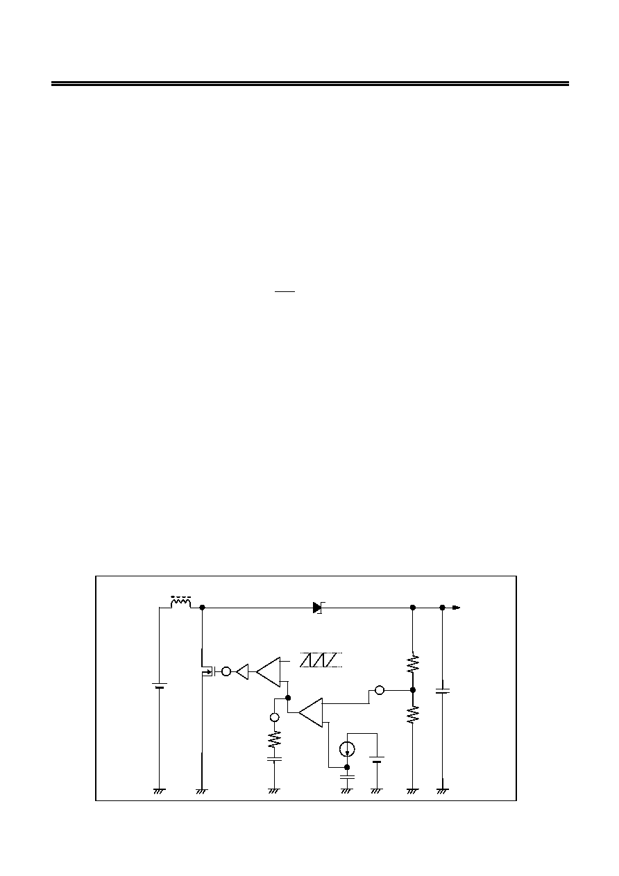
4. Timer latch short-circuit protection function
This IC has a timer latch short-circuit protection circuit that stops the switching operation when the
output voltage drops for a specific time due to output short-circuiting. A capacitor (CSP) that is used
to set the delay time of this short-circuit protection circuit is connected to the CSP pin.
This IC operates at the maximum duty ratio if the output voltage drops due to output short-circuiting.
At the maximum duty ratio, constant-current charging of CSP starts. If this status lasts for a specific
time and the CSP pin voltage rises above the reference voltage (1 V), the latch mode is set. Note that
the latch mode is different from the shutdown status in that the switching operation is stopped but the
internal circuitry operates normally.
To reset the latch operation to protect the IC from short-circuiting, either lower V
IN
to the timer latch
reset voltage or lower or lower the level of the shutdown pin to "L". Note that the latch operation is not
reset even if V
IN
falls below the UVLO voltage.
5. UVLO function
This IC includes a UVLO (under-voltage lockout) circuit to prevent the IC from malfunctioning due to a
transient status when power is applied or a momentary drop of the supply voltage. When UVLO is in
the detection state, switching is stopped and the external FET is held in the off status. Once UVLO
enters the detection state, the soft-start function is reset.
Note that the other internal circuits operate normally and that the status is different from the power-off
status
STEP-UP, HIGH-FREQUENCY, PWM CONTROL SWITCHING REGULATOR CONTROLLERS
Rev.2.0
_00
S-8337/8338 Series
Seiko Instruments Inc.
13
6. Error amplifier
The error amplifier outputs the PWM control signal so that the voltage of the FB pin is held at a specific
value (1 V). By connecting a resistor (RZ) and capacitor (CZ) to the output pin (CC pin) of the error
amplifier in series, an optional loop gain can be set, enabling stabilized phase compensation.
7. Operation
The following are basic equations [(1) through (7)] of the step-up switching regulator (refer to
Figure 9).
D
L
C
L
M1
FB
CONT
V
IN
EXT
VSS
V
OUT
Figure 9 Step-up Switching Regulator Circuit for Basic Equations
Voltage at the CONT pin at the moment M1 is turned ON (current I
L
flowing through L is zero), V
A
:
V
A
= V
S
*1
................................................................................................................(1)
*1. V
S
: Non-saturated voltage of M1
Change in I
L
over time:
L
V
V
L
V
dt
dl
S
IN
L
L
-
=
=
..................................................................................................(2)
Integration of the above equation:
t
L
V
V
I
S
IN
L
∑
-
=
.....................................................................................................(3)
I
L
flows while M1 is ON (t
on
). This time is determined by the oscillation frequency of OSC.
Peak current (I
PK
) after t
ON
:
ON
S
IN
PK
t
L
V
V
I
∑
-
=
................................................................................................(4)
The energy stored in L is represented by
∑ L(I
PK
)
2
.
When M1 is turned OFF (t
OFF
), the energy stored in L is released via a diode, generating a reverse
voltage (V
L
).
V
L
:
(
)
IN
D
OUT
L
V
V
V
V
-
+
=
*2
.............................................................................................(5)
*2. V
D
: Diode forward voltage
The voltage on the CONT pin rises only by V
OUT
+ V
D
.
1
2

STEP-UP, HIGH-FREQUENCY, PWM CONTROL SWITCHING REGULATOR CONTROLLERS
S-8337/8338 Series
Rev.2.0
_00
14
Seiko Instruments Inc.
Change in current (I
L
) flowing through the diode into V
OUT
during t
OFF
:
L
V
V
V
L
V
dt
dl
IN
D
OUT
L
L
-
+
=
=
.........................................................................................(6)
Integration of the above equation is as follows:
t
L
V
V
V
I
I
IN
D
OUT
PK
L
∑
-
+
-
=
....................................................................................(7)
During t
ON
, energy is stored in L and is not transmitted to V
OUT
. When receiving output current (I
OUT
)
from V
OUT
, the energy of the capacitor (C
L
) is used. As a result, the pin voltage of C
L
is reduced, and
goes to the lowest level after M1 is turned ON (t
ON
). When M1 is turned OFF, the energy stored in L is
transmitted via the diode to C
L
, and the pin voltage of C
L
rises drastically. Because V
OUT
is a time
function indicating the maximum value (ripple voltage: V
p-p
) when the current flowing through the
diode into V
OUT
and the load current I
OUT
match.
Next, this ripple voltage is determined as follows.
I
OUT
vs t
1
(time) from when M1 is turned OFF (after t
ON
) to when V
OUT
reaches the maximum level:
1
IN
D
OUT
PK
OUT
t
L
V
V
V
I
I
∑
-
+
-
=
..................................................................................(8)
(
)
-
+
∑
-
=
IN
D
OUT
OUT
PK
1
V
V
V
L
I
I
t
..............................................................................(9)
When M1 is turned ON (after t
OFF
), I
L
= 0 (when the energy of the inductor is completely transmitted):
Based on equation (7),
PK
OFF
IN
D
OUT
I
t
V
V
V
L
=
-
+
..........................................................................................(10)
When substituting equation (10) for equation (9):
OFF
PK
OUT
OFF
1
t
I
I
t
t
∑
-
=
.............................................................................................(11)
Electrical charge
Q
1
which is charged in C
L
during t
1
:
2
1
IN
D
OUT
1
PK
1
t
0
IN
D
OUT
1
t
0
PK
L
1
t
0
1
t
2
1
L
V
V
V
t
I
tdt
L
V
V
V
dt
I
dt
I
Q
∑
-
+
-
∑
=
∑
-
+
-
∑
=
=
................(12)
When substituting equation (12) for equation (9):
(
)
1
OUT
PK
1
OUT
PK
PK
1
t
2
I
I
t
I
I
2
1
I
Q
∑
+
=
∑
-
-
=
....................................................................(13)
A rise voltage (V
p-p
) due to
Q
1
:
1
OUT
PK
L
L
1
p
p
t
2
I
I
C
1
C
Q
V
∑
+
∑
=
=
-
...................................................................................(14)
When taking into consideration I
OUT
consumed during t
1
and ESR
*1
(R
ESR
) of C
L
:
L
1
OUT
ESR
OUT
PK
1
OUT
PK
L
L
1
p
p
C
t
I
R
2
I
I
t
2
I
I
C
1
C
Q
V
∑
-
∑
+
+
∑
+
∑
=
=
-
......................................(15)
*1. Equivalent Series Resistance

STEP-UP, HIGH-FREQUENCY, PWM CONTROL SWITCHING REGULATOR CONTROLLERS
Rev.2.0
_00
S-8337/8338 Series
Seiko Instruments Inc.
15
When substituting equation (11) for equation (15):
(
)
ESR
OUT
PK
L
OFF
PK
2
OUT
PK
p
p
R
2
I
I
C
t
I
2
I
I
V
∑
+
+
∑
-
=
-
..............................................................(16)
Therefore to reduce the ripple voltage, it is important that the capacitor connected to the output pin
has a large capacity and a small ESR.

STEP-UP, HIGH-FREQUENCY, PWM CONTROL SWITCHING REGULATOR CONTROLLERS
S-8337/8338 Series
Rev.2.0
_00
16
Seiko Instruments Inc.
External Parts Selection
1. Inductor
The inductance has a strong influence on the maximum output current (I
OUT
) and efficiency (
).
The peak current (I
PK
) increases by decreasing L and the stability of the circuit improves and I
OUT
increases. If L is decreased further, the efficiency falls, and I
OUT
decreases if the current drive
capability of the external transistor is insufficient.
The loss of I
PK
by the switching transistor decreases by increasing L and the efficiency becomes
maximum at a certain L value. Further increasing L decrease the efficiency due to the loss of the DC
resistance of the inductor. I
OUT
also decreases.
If the oscillation frequency is higher, a smaller L value can be chosen, making the inductor smaller. In
the S-8337/8338 Series, the oscillation frequency can be varied within the range of 286 kHz to 1.133
MHz by the external resistor, so select an L value best suited to the frequency. The recommended
value is between 2.2
ĶH and 22 ĶH.
When selecting an inductor, note the allowable current of the inductor. If a current exceeding this
allowable current flows through the inductor, magnetic saturation occurs, substantially lowering the
efficiency and increasing the current, which results in damage to the IC.
Therefore, select an inductor so that I
PK
does not exceed the allowable current. I
PK
is expressed by
the following equations in the discontinuous mode and continuous mode.
)
mode
ous
discontinu
(
L
fosc
)
V
V
(V
I
2
I
IN
D
OUT
OUT
PK
∑
-
+
=
..................................................................(17)
mode)
s
(continuou
L
fosc
)
V
(V
2
V
)
V
V
(V
I
V
V
V
I
D
OUT
IN
IN
D
OUT
OUT
IN
D
OUT
PK
∑
∑
+
∑
∑
-
+
+
∑
+
=
................................................................(18)
f
OSC
= Oscillation frequency, V
D
0.4 V.
2. Diode
Use an external diode that meets the following requirements.
∑ Low forward voltage
∑ High switching speed
∑ Reverse breakdown voltage: V
OUT
+ [Spike voltage] or more
∑ Rated current: I
PK
or more
3. Capacitors (C
IN
, C
L
)
The capacitor on the input side (C
IN
) can lower the supply impedance and level the input current for
better efficiency. Select C
IN
according to the impedance of the power supply to be used.
The capacitor on the output side (C
L
) is used to smooth the output voltage. Select an appropriate
capacitance value based on the I/O conditions and load conditions. A capacitance of 10
ĶF or more is
recommended.
By adjusting the phase compensation of the feedback loop using the external resistor (RZ) and
capacitor (CZ), a ceramic capacitor can be used as the capacitor on the output side. If a capacitor
whose equivalent series resistance is between 30 m
and 500 m is used as the output capacitor, the
adjustable range of the phase compensation is wider; however, note that other characteristics may be
affected by ripple voltage or other conditions at this time. The optimal capacitor differs depending on
the L value, capacitance value, wiring, and application (output load), so select the capacitor after
performing sufficient evaluation under the actual usage conditions.
STEP-UP, HIGH-FREQUENCY, PWM CONTROL SWITCHING REGULATOR CONTROLLERS
Rev.2.0
_00
S-8337/8338 Series
Seiko Instruments Inc.
17
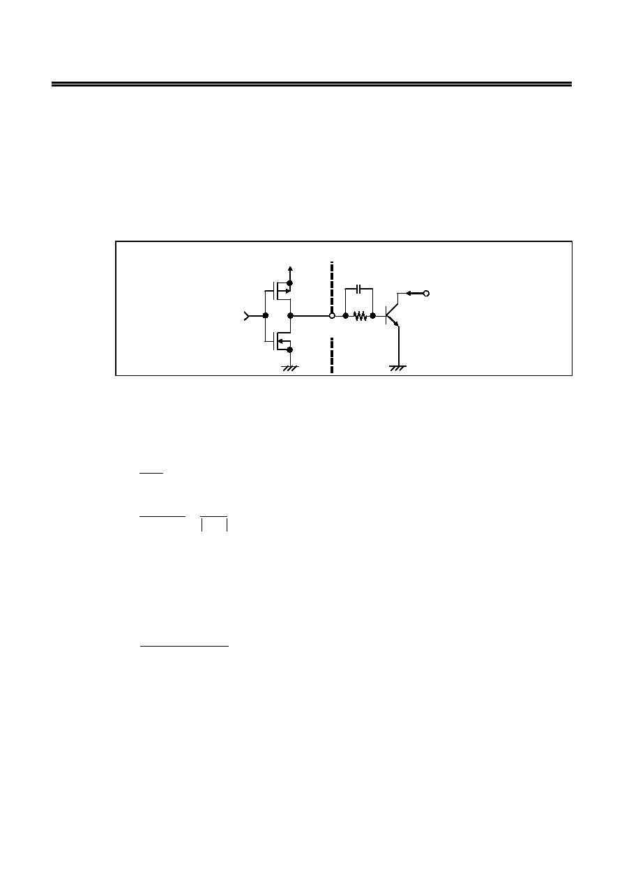
4. External transistor
A bipolar (NPN) or enhancement (N-channel) MOS FET transistor can be used as the external
capacitor.
4-1. Bipolar (NPN) type
The driving capability when the output current is increased by using a bipolar transistor is
determined by h
FE
and R
b
of the bipolar transistor. Figure 10 shows a peripheral circuit.
Nch
Pch
R
b
V
IN
I
PK
EXT
C
b
2200 pF
1 k
Figure 10 External Transistor Periphery
1 k
is recommended for R
b
. Actually, calculate the necessary base current (I
b
) from h
FE
of the
bipolar transistor as follows and select an R
b
value lower than this.
I
b
=
h
FE
I
PK
R
b
=
I
b
V
IN
≠ 0.7
≠
I
EXTH
0.4
A small R
b
increases the output current, but the efficiency decreases. Actually, a pulsating
current flows and a voltage drop occurs due to the wiring capacitance. Determine the optimum
value by experiment.
A speed-up capacitor (C
b
) connected in parallel with R
b
resistance as shown in Figure 10
decreases the switching loss and improves the efficiency.
Select C
b
by observing the following equation.
C
b
2
∑ R
b
∑ f
OSC
∑ 0.7
1
However, in practice, the optimum C
b
value also varies depending on the characteristics of the
bipolar transistor employed. Therefore, determine the optimum value of C
b
by experiment.

STEP-UP, HIGH-FREQUENCY, PWM CONTROL SWITCHING REGULATOR CONTROLLERS
S-8337/8338 Series
Rev.2.0
_00
18
Seiko Instruments Inc.
4-2. Enhancement MOS FET type
Use an Nch power MOS FET. For high efficiency, using a MOS FET with a low ON resistance
(R
ON
) and small input capacitance (C
ISS
) is ideal, however, ON resistance and input capacitance
generally share a trade-off relationship. The ON resistance is efficient in a range in which the
output current is relatively great during low-frequency switching, and the input capacitance is
efficient in a range in which the output current is middling during high-frequency switching. Select
a MOS FET whose ON resistance and input capacitance are optimal depending on the usage
conditions.
The input voltage (V
IN
) is supplied for the gate voltage of the MOS FET, so select a MOS FET with
a gate withstanding voltage that is equal to the maximum usage value of the input voltage or
higher and a drain withstanding voltage that is equal to the amount of the output voltage (V
OUT
)
and diode voltage (V
D
) or higher.
If a MOS FET with a threshold that is near the UVLO detection voltage is used, a large current
may flow, stopping the output voltage from rising and possibly generating heat in the worst case.
Select a MOS FET with a threshold that is sufficiently lower than the UVLO detection voltage
value.
STEP-UP, HIGH-FREQUENCY, PWM CONTROL SWITCHING REGULATOR CONTROLLERS
Rev.2.0
_00
S-8337/8338 Series
Seiko Instruments Inc.
19
5. Oscillation frequency and maximum duty ratio setting resistors (ROSC, RDuty)
With the S-8337/8338 Series, the oscillation frequency can be set in a range of 286 kHz to 1.133 MHz
using external resistance. Connect a resistor across the ROSC and VSS pins. Select the resistor by
using the following equation and referring to Figure 11. However, the following equation and figure
assume that the resistance value is the desired value and show the theoretical values when the IC is
in the typical conditions. Note that fluctuations of resistance and IC are not considered.
140
∑
10
3
R
OSC
[k
]
f
OSC
[kHz]
1400
1200
1000
800
600
400
200
0
0
200
400
600
f
OS
C
[k
Hz]
R
OSC
[k
]
Figure 11 R
OSC
vs. f
OSC
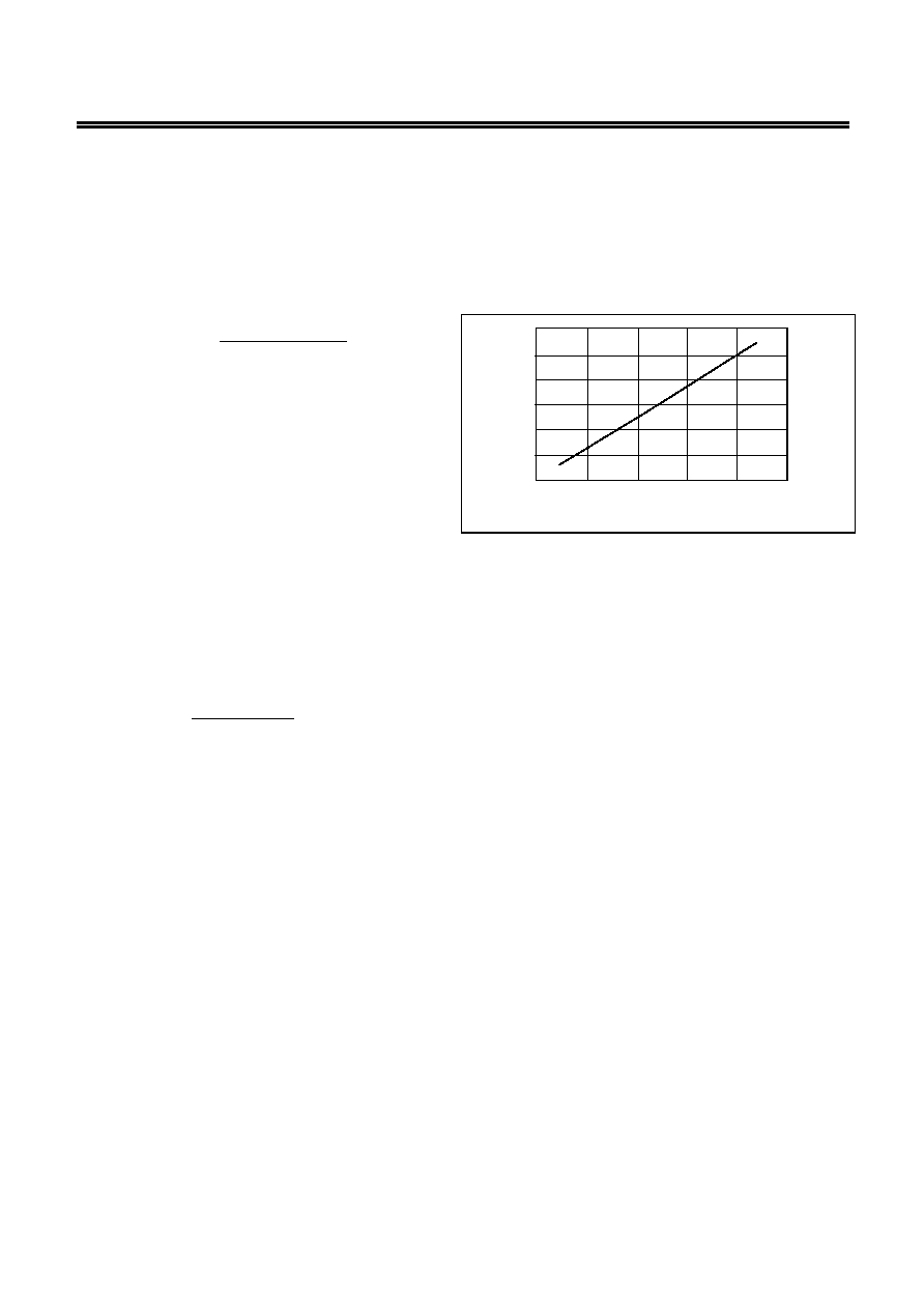
With the S-8337 Series, the maximum duty ratio can be set in a range of 47% to 88.5% by an external
resistor. Connect the resistor across the RDuty and VSS pins. Select the resistance by using the
following equation and referring to Figure 12. The maximum duty ratio fluctuates according to the
oscillation frequency. If the value of ROSC is changed, therefore, be sure to change the value of
RDuty so that it is always in proportion to ROSC. However, the following equation and figure assume
that the resistance value is the desired value and show the theoretical values when the IC is in the
typical conditions. Note that fluctuations of resistance and IC are not considered.
(94.5
- MaxDuty)
R
OSC
R
Duty
11.5
100
90
80
70
60
50
40
0
2
4
5
Ma
x
D
u
t
y [
%
]
R
Duty
/R
OSC
1
3
Figure 12 R
Duty
/R
OSC
vs. MaxDuty
Connect resistors ROSC and RDuty as close to the IC as possible.
STEP-UP, HIGH-FREQUENCY, PWM CONTROL SWITCHING REGULATOR CONTROLLERS
S-8337/8338 Series
Rev.2.0
_00
20
Seiko Instruments Inc.
6. Short-circuit protection delay time setting capacitor (CSP)
With the S-8337/8338 Series, the short-circuit protection delay time can be set to any value by an
external capacitor. Connect the capacitor across the CSP and VSS pins. Select the capacitance by
using the following equation and referring to Figure 13. However, the following equation and figure
assume that the capacitor value is the desired value and show the theoretical values when the IC is in
the typical conditions. Note that fluctuations of capacitor and IC are not considered.
C
SP
[
ĶF]
1.0
t
PRO
[ms]
∑
2
∑
10
-3
120
100
80
60
40
20
0
0
0.10
0.20
0.25
t
PR
O
[m
s]
C
SP
[
ĶF]
0.05
0.15
Figure 13 C
SP
vs. t
PRO
7. Output voltage setting resistors (RFB1, RBF2)
With the S-8337/8338 Series, the output voltage can be set to any value by external divider resistors.
Connect the divider resistors across the V
OUT
and VSS pins. Because V
FB
= 1 V, the output voltage
can be calculated by this equation.
=
V
OUT
R
FB2
(R
FB1
+ R
FB2
)
Connect divider resistors RFB1 and RFB2 as close to the IC to minimize effects from of noise. If noise
does have an effect, adjust the values of RFB1 and RFB2 so that R
FB1
+ R
FB2
< 100 k
.
CFB connected in parallel with RFB1 is a capacitor for phase compensation. Select the optimum
value of this capacitor at which the stable operation can be ensured from the values of the inductor
and output capacitor.
8. Phase compensation setting resistor and capacitor (RZ, CZ)
The S-8337/8338 Series needs appropriate compensation for the voltage feedback loop to prevent
excessive output ripple and unstable operation from deteriorating the efficiency. This compensation is
implemented by connecting RZ and CZ in series across the CC and VSS pins. RZ sets the
high-frequency gain for a high-speed transient response. CZ sets the pole and zero of the error
amplifier and keeps the loop stable. Adjust RZ and CZ, taking into consideration conditions such as
the inductor, output capacitor, and load current, so that the optimum transient characteristics can be
obtained.
STEP-UP, HIGH-FREQUENCY, PWM CONTROL SWITCHING REGULATOR CONTROLLERS
Rev.2.0
_00
S-8337/8338 Series
Seiko Instruments Inc.
21
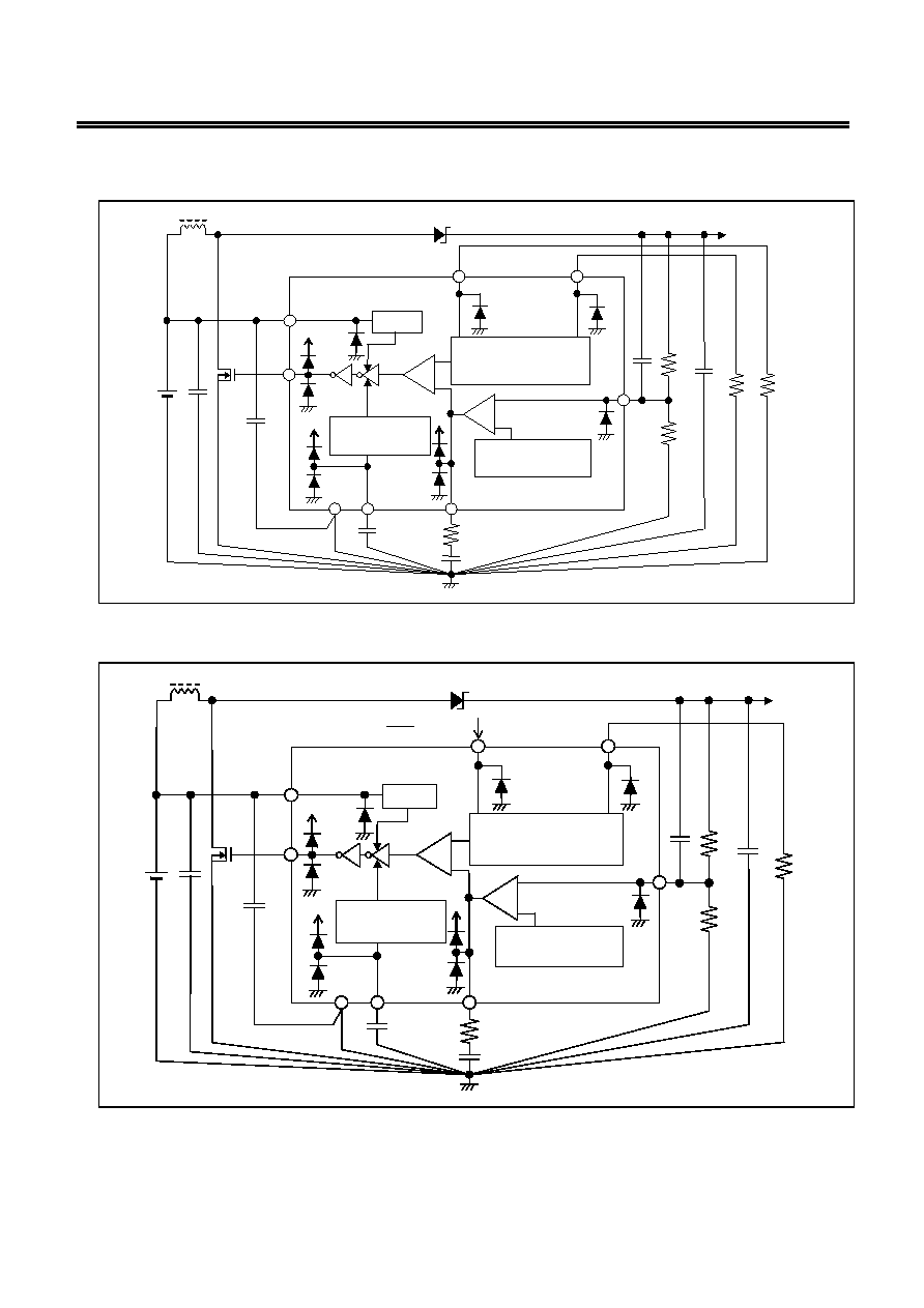
Standard Circuits
PWM
comparator
V
OUT
Timer latch
short-circuit
protection circuit
RDuty (S-8337)
RFB2
VSS
RFB1
FB
SD
L
VIN
EXT
UVLO
CSP
CC
RZ
CZ
ROSC
M1
CFB
+
-
+
-
C
IN
Oscillator
Maximum duty circuit
Reference voltage
(1.0 V)
soft-start circuit
Error amplifier
0.1
ĶF
ROSC RDuty
C
L
Ground point
Figure 14 Standard Circuit (S-8337 Series)
PWM
comparator
V
OUT
Timer latch
short-circuit
protection circuit
RFB2
VSS
RFB1
FB
SD
L
VIN
EXT
UVLO
CSP
CC
RZ
CZ
ROSC
M1
CFB
+
-
+
-
C
IN
Oscillator
Maximum duty circuit
Reference voltage
(1.0 V)
soft-start circuit
Error amplifier
0.1
ĶF
ROSC
C
L
ON/OFF (S-8338)
Ground point
Figure 15 Standard Circuit (S-8338 Series)
Caution The above connection diagram and constant will not guarantee successful operation.
Perform thorough evaluation using the actual application to set the constant.
STEP-UP, HIGH-FREQUENCY, PWM CONTROL SWITCHING REGULATOR CONTROLLERS
S-8337/8338 Series
Rev.2.0
_00
22
Seiko Instruments Inc.
Power Dissipation of Package
0
50
100
150
600
400
200
0
Power
Dissipation
P
D
(mW)
8-Pin TSSOP
8-Pin SON(A)
Ambient Temperature Ta (
įC)
Figure 16 Power Dissipation of Package (Before Mounting)
Precaution
∑ Mount external capacitors, diodes, and inductor as close as possible to the IC.
∑ Characteristics ripple voltage and spike noise occur in IC containing switching regulators. Moreover
rush current flows at the time of a power supply injection. Because these largely depend on the inductor,
the capacitor and impedance of power supply used, fully check them using an actually mounted model.
∑ Make sure the dissipation of the switching transistor (especially at a high temperature) does not exceed
the allowable power dissipation of the package.
∑ The performance of a switching regulator varies depending on the design of the PCB patterns,
peripheral circuits, and external parts. Thoroughly test all settings with your device.
∑ This IC builds in soft start function, starts reference voltage gradually, and it is controlled so that FB pin
voltage and reference voltage become this potential. Therefore, keep in mind that it will be in a
maximum duty state according to the factor of IC exterior if FB pin voltage is held less than reference
voltage.
∑ Although the IC contains a static electricity protection circuit, static electricity or voltage that exceeds
the limit of the protection circuit should not be applied.
∑ Seiko Instruments Inc. assumes no responsibility for the way in which this IC is used on products
created using this IC or for the specifications of that product, nor does Seiko Instruments Inc. assume
any responsibility for any infringement of patents or copyrights by products that include this IC either in
Japan or in other countries.

STEP-UP, HIGH-FREQUENCY, PWM CONTROL SWITCHING REGULATOR CONTROLLERS
Rev.2.0
_00
S-8337/8338 Series
Seiko Instruments Inc.
23
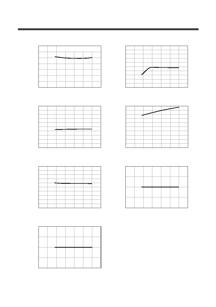
Example of Major Temperature Characteristics (Ta
=
=
=
= ----40 to 85įįįįC)
I
SS1
vs. Ta (V
IN
= 3.3 V)
700
600
500
400
300
200
100
0
-40 -20 0 20 40 60 80 100
Ta [
įC]
I
SS1
[
ĶA]
f
OSC
= 1133 kHz (R
OSC
= 120 k)
f
OSC
= 700 kHz (R
OSC
= 200 k)
f
OSC
= 286 kHz (R
OSC
= 510 k)
I
SSS
vs. Ta (V
IN
= 3.3 V)
1.0
0.9
0.8
0.7
0.6
0.5
0.4
0.3
0.2
0.1
0
-40 -20 0 20 40 60 80 100
Ta [
įC]
I
SSS
[
ĶA]
f
OSC
= 700 kHz (R
OSC
= 200 k)
≠200
≠180
≠160
≠140
≠120
≠100
≠80
≠60
≠40
≠20
0
-40 -20 0 20 40 60 80 100
Ta [
įC]
I
EXTH
[mA]
I
EXTH
vs. Ta (V
IN
= 3.3 V)
f
OSC
= 700 kHz, MaxDuty = 77% (R
OSC
= 200 k, R
Duty
= 300 k)
200
180
160
140
120
100
80
60
40
20
0
-40 -20 0 20 40 60 80 100
Ta [
įC]
I
EXTL
[mA]
I
EXTL
vs. Ta (V
IN
= 3.3 V)
f
OSC
= 700 kHz, MaxDuty = 77% (R
OSC
= 200 k, R
Duty
= 300 k)
0.10
0.08
0.06
0.04
0.02
0
≠0.02
≠0.04
≠0.06
≠0.08
≠0.10
-40 -20 0 20 40 60 80 100
Ta [
įC]
I
FB
[
ĶA]
I
FB
vs. Ta (V
IN
= 3.3 V)
f
OSC
vs. Ta (V
IN
= 3.3 V)
1400
1200
1000
800
600
400
200
0
-40 -20 0 20 40 60 80 100
Ta [
įC]
f
OSC
[kHz]
f
OSC
= 1133 kHz (R
OSC
= 120 k)
f
OSC
= 700 kHz (R
OSC
= 200 k)
f
OSC
= 286 kHz (R
OSC
= 510 k)
100
90
80
70
60
50
40
30
20
10
0
-40 -20 0 20 40 60 80 100
Ta [
įC]
MaxDuty
[%]
MaxDuty vs. Ta (V
IN
= 3.3 V)
MaxDuty
= 88.5% (R
OSC
= 200 k, R
Duty
= 100 k)
MaxDuty
= 77% (R
OSC
= 200 k, R
Duty
= 300 k)
MaxDuty
= 47% (R
OSC
= 200 k, R
Duty
= 820 k)
t
SS
vs. Ta (V
IN
= 3.3 V)
25.0
20.0
15.0
10.0
5.0
0
-40 -20 0 20 40 60 80 100
Ta [
įC]
t
SS
[ms]
t
SS
= 10 ms
t
SS
= 20 ms
STEP-UP, HIGH-FREQUENCY, PWM CONTROL SWITCHING REGULATOR CONTROLLERS
S-8337/8338 Series
Rev.2.0
_00
24
Seiko Instruments Inc.
70.0
60.0
50.0
40.0
30.0
20.0
10.0
0
-40 -20 0 20 40 60 80 100
Ta [
įC]
t
PRO
[ms]
t
PRO
vs. Ta (V
IN
= 3.3 V)
t
PRO
= 50 ms (CSP
= 0.1 ĶF)
V
UVLO
vs. Ta
2.5
2.0
1.5
1.0
0.5
0
-40 -20 0 20 40 60 80 100
Ta [
įC]
V
UVLO
[V]
V
UVLO
= 2.3 V
V
UVLO
= 1.5 V
0.35
0.30
0.25
0.20
0.15
0.10
0.05
0
-40 -20 0 20 40 60 80 100
Ta [
įC]
V
UVLOHYS
[V]
V
UVLOHYS
vs. Ta
V
UVLOHYS
= 0.3 V
V
UVLOHYS
= 0.1 V
≠100
≠90
≠80
≠70
≠60
≠50
≠40
≠30
≠20
≠10
0
-40 -20 0 20 40 60 80 100
Ta [
įC]
I
CCH
[
ĶA]
I
CCH
vs. Ta (V
IN
= 3.3 V)
100
90
80
70
60
50
40
30
20
10
0
-40 -20 0 20 40 60 80 100
Ta [
įC]
I
CCL
[
ĶA]
I
CCL
vs. Ta (V
IN
= 3.3 V)
1.2
1.0
0.8
0.6
0.4
0.2
0
-40 -20 0 20 40 60 80 100
Ta [
įC]
V
RTLT
[V]
V
RTLT
vs. Ta (V
IN
= 3.3 V)
1.0
0.9
0.8
0.7
0.6
0.5
0.4
0.3
0.2
0.1
0
-40 -20 0 20 40 60 80 100
Ta [
įC]
V
SH
[V]
V
SH
vs. Ta (V
IN
= 3.3 V)
1.0
0.9
0.8
0.7
0.6
0.5
0.4
0.3
0.2
0.1
0
-40 -20 0 20 40 60 80 100
Ta [
įC]
V
SL
[V]
V
SL
vs. Ta (V
IN
= 3.3 V)

STEP-UP, HIGH-FREQUENCY, PWM CONTROL SWITCHING REGULATOR CONTROLLERS
Rev.2.0
_00
S-8337/8338 Series
Seiko Instruments Inc.
25
0.1
0
≠0.1
-40 -20 0 20 40 60 80 100
Ta [
įC]
I
SH
[
ĶA]
I
SH
vs. Ta (V
IN
= 3.3 V)
0.1
0
≠0.1
-40 -20 0 20 40 60 80 100
Ta [
įC]
I
SL
[
ĶA]
I
SL
vs. Ta (V
IN
= 3.3 V)
STEP-UP, HIGH-FREQUENCY, PWM CONTROL SWITCHING REGULATOR CONTROLLERS
S-8337/8338 Series
Rev.2.0
_00
26
Seiko Instruments Inc.
Example of Major Power Supply Dependence Characteristics (Ta
=
=
=
= 25įįįįC)
I
SS1
vs. V
IN
1200
1000
800
600
400
200
0
0 1 2 3 4 5 6 7
V
IN
[V]
I
SS1
[
ĶA]
f
OSC
= 1133 kHz
(R
OSC
= 120 k)
f
OSC
= 700 kHz
(R
OSC
= 200 k)
f
OSC
= 286 kHz
(R
OSC
= 510 k)
I
SSS
vs. V
IN
1.0
0.9
0.8
0.7
0.6
0.5
0.4
0.3
0.2
0.1
0
I
SSS
[
ĶA]
f
OSC
= 700 kHz (R
OSC
= 200 k)
0 1 2 3 4 5 6 7
V
IN
[V]
≠200
≠180
≠160
≠140
≠120
≠100
≠80
≠60
≠40
≠20
0
I
EXTH
[mA]
I
EXTH
vs. V
IN
0 1 2 3 4 5 6 7
V
IN
[V]
f
OSC
= 700 kHz, MaxDuty = 77% (R
OSC
= 200 k, R
Duty
= 300 k)
200
180
160
140
120
100
80
60
40
20
0
I
EXTL
[mA]
I
EXTL
vs. V
IN
f
OSC
= 700 kHz, MaxDuty = 77% (R
OSC
= 200 k, R
Duty
= 300 k)
0 1 2 3 4 5 6 7
V
IN
[V]
0.10
0.08
0.06
0.04
0.02
0
≠0.02
≠0.04
≠0.06
≠0.08
≠0.10
I
FB
[
ĶA]
I
FB
vs. V
IN
0 1 2 3 4 5 6 7
V
IN
[V]
f
OSC
vs. V
IN
1400
1200
1000
800
600
400
200
0
f
OSC
[kHz]
0 1 2 3 4 5 6 7
V
IN
[V]
f
OSC
= 1133 kHz (R
OSC
= 120 k)
f
OSC
= 700 kHz (R
OSC
= 200 k)
f
OSC
= 286 kHz (R
OSC
= 510 k)
100
90
80
70
60
50
40
30
20
10
0
MaxDuty
[%]
MaxDuty vs. V
IN
0 1 2 3 4 5 6 7
V
IN
[V]
MaxDuty
= 88.5%
MaxDuty
= 47%
MaxDuty
= 77%
(R
OSC
= 200 k, R
Duty
= 100 k) (R
OSC
= 200 k, R
Duty
= 300 k)
(R
OSC
= 200 k, R
Duty
= 820 k)
t
SS
vs. V
IN
25.0
20.0
15.0
10.0
5.0
0
t
SS
[ms]
0 1 2 3 4 5 6 7
V
IN
[V]
t
SS
= 10 ms
t
SS
= 20 ms
STEP-UP, HIGH-FREQUENCY, PWM CONTROL SWITCHING REGULATOR CONTROLLERS
Rev.2.0
_00
S-8337/8338 Series
Seiko Instruments Inc.
27
70.0
60.0
50.0
40.0
30.0
20.0
10.0
0
t
PRO
[ms]
t
PRO
vs. V
IN
0 1 2 3 4 5 6 7
V
IN
[V]
t
PRO
= 50 ms (CSP
= 0.1 ĶF)
≠100
≠90
≠80
≠70
≠60
≠50
≠40
≠30
≠20
≠10
0
I
CCH
[
ĶA]
I
CCH
vs. V
IN
0 1 2 3 4 5 6 7
V
IN
[V]
100
90
80
70
60
50
40
30
20
10
0
I
CCL
[
ĶA]
I
CCL
vs. V
IN
0 1 2 3 4 5 6 7
V
IN
[V]
1.0
0.9
0.8
0.7
0.6
0.5
0.4
0.3
0.2
0.1
0
V
SH
[V]
V
SH
vs. V
IN
0 1 2 3 4 5 6 7
V
IN
[V]
1.0
0.9
0.8
0.7
0.6
0.5
0.4
0.3
0.2
0.1
0
V
SL
[V]
V
SL
vs. V
IN
0 1 2 3 4 5 6 7
V
IN
[V]
0.1
0
≠0.1
I
SH
[
ĶA]
I
SH
vs. V
IN
0 1 2 3 4 5 6 7
V
IN
[V]
0.1
0
≠0.1
I
SL
[
ĶA]
I
SL
vs. V
IN
0 1 2 3 4 5 6 7
V
IN
[V]
STEP-UP, HIGH-FREQUENCY, PWM CONTROL SWITCHING REGULATOR CONTROLLERS
S-8337/8338 Series
Rev.2.0
_00
28
Seiko Instruments Inc.
Example of External Parts Dependence Characteristics
f
OSC
vs. R
OSC
(V
IN
= 3.3 V)
1600
1400
1200
1000
800
600
400
200
0
0 100
200 300 400 500 600
R
OSC
[k
]
f
OSC
[kHz]
Ta
= ≠40įC
Ta
= 25įC
Ta
= 85įC
f
OSC
vs. R
OSC
(V
IN
= 5.0 V)
1600
1400
1200
1000
800
600
400
200
0
0 100
200 300 400 500 600
R
OSC
[k
]
f
OSC
[kHz]
Ta
= ≠40įC
Ta
= 25įC
Ta
= 85įC
100
90
80
70
60
50
40
30
20
10
0
MaxDuty
[%]
MaxDuty vs. R
Duty
/R
OSC
(R
OSC
= 200 k, V
IN
= 3.3 V)
0 0.5 1 1.5 2 2.5 3 3.5
R
Duty
/R
OSC
4 4.5 5
Ta
= ≠40įC
Ta
= 25įC
Ta
= 85įC
100
90
80
70
60
50
40
30
20
10
0
MaxDuty
[%]
MaxDuty vs. R
Duty
/R
OSC
(R
OSC
= 200 k, V
IN
= 5.0 V)
0 0.5 1 1.5 2 2.5 3 3.5
R
Duty
/R
OSC
4 4.5 5
Ta
= ≠40įC
Ta
= 25įC
Ta
= 85įC
t
PRO
vs. CSP (V
IN
= 3.3 V)
350
300
250
200
150
100
50
0
0 0.1 0.2 0.3 0.4 0.5
CSP [
ĶF]
t
PRO
[ms]
Ta
= ≠40įC
Ta
= 25įC
Ta
= 85įC
t
PRO
vs. CSP (V
IN
= 5.0 V)
350
300
250
200
150
100
50
0
0 0.1 0.2 0.3 0.4 0.5
CSP [
ĶF]
t
PRO
[ms]
Ta
= ≠40įC
Ta
= 25įC
Ta
= 85įC

STEP-UP, HIGH-FREQUENCY, PWM CONTROL SWITCHING REGULATOR CONTROLLERS
Rev.2.0
_00
S-8337/8338 Series
Seiko Instruments Inc.
29
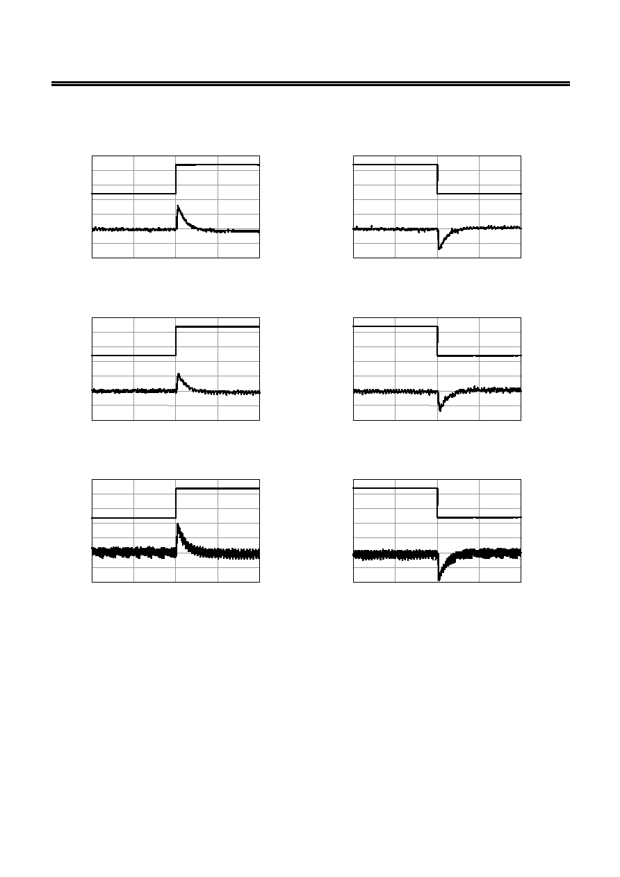
Examples of Transient Response Characteristics
1. Powering ON (V
OUT
=
=
=
= 9.2 V, V
IN
=
=
=
= 0 V3.3 V, Ta ==== 25įįįįC)
1-1. f
OSC
= 1133 kHz, I
OUT
= 0 mA, t
SS
= 10 ms
1-2. f
OSC
= 1133 kHz, I
OUT
= 100 mA, t
SS
= 10 ms
0
2
≠5 0 5 10 15 20
time [ms]
V
IN
[V]
0
4
8 V
OUT
[V]
4
12
0
2
≠5 0 5 10 15 20
time [ms]
V
IN
[V]
0
4
8 V
OUT
[V]
4
12
1-3. f
OSC
= 700 kHz, I
OUT
= 0 mA, t
SS
= 10 ms
1-4. f
OSC
= 700 kHz, I
OUT
= 100 mA, t
SS
= 10 ms
0
2
≠5 0 5 10 15 20
time [ms]
V
IN
[V]
0
4
8 V
OUT
[V]
4
12
0
2
≠5 0 5 10 15 20
time [ms]
V
IN
[V]
0
4
8 V
OUT
[V]
4
12
1-5. f
OSC
= 286 kHz, I
OUT
= 0 mA, t
SS
= 10 ms
1-6. f
OSC
= 286 kHz, I
OUT
= 100 mA, t
SS
= 10 ms
0
2
≠5 0 5 10 15 20
time [ms]
V
IN
[V]
0
4
8 V
OUT
[V]
4
12
0
2
≠5 0 5 10 15 20
time [ms]
V
IN
[V]
0
4
8 V
OUT
[V]
4
12
STEP-UP, HIGH-FREQUENCY, PWM CONTROL SWITCHING REGULATOR CONTROLLERS
S-8337/8338 Series
Rev.2.0
_00
30
Seiko Instruments Inc.
2. Responses of shutdown pin (V
OUT
=
=
=
= 9.2 V, V
ON/OFF
=
=
=
= 0 V3.3 V)
2-1. f
OSC
= 1133 kHz, I
OUT
= 0 mA, t
SS
= 10 ms
2-2. f
OSC
= 1133 kHz, I
OUT
= 100 mA, t
SS
= 10 ms
0
2
≠5 0 5 10 15 20
time [ms]
0
4
8 V
OUT
[V]
4
12
V
ON/OFF
[V]
0
2
≠5 0 5 10 15 20
time [ms]
0
4
8 V
OUT
[V]
4
12
V
ON/OFF
[V]
2-3. f
OSC
= 700 kHz, I
OUT
= 0 mA, t
SS
= 10 ms
2-4. f
OSC
= 700 kHz, I
OUT
= 100 mA, t
SS
= 10 ms
0
2
≠5 0 5 10 15 20
time [ms]
0
4
8 V
OUT
[V]
4
12
V
ON/OFF
[V]
0
2
≠5 0 5 10 15 20
time [ms]
0
4
8 V
OUT
[V]
4
12
V
ON/OFF
[V]
2-5. f
OSC
= 286 kHz, I
OUT
= 0 mA, t
SS
= 10 ms
2-6. f
OSC
= 286 kHz, I
OUT
= 100 mA, t
SS
= 10 ms
0
2
≠5 0 5 10 15 20
time [ms]
0
4
8 V
OUT
[V]
4
12
V
ON/OFF
[V]
0
2
≠5 0 5 10 15 20
time [ms]
0
4
8 V
OUT
[V]
4
12
V
ON/OFF
[V]
STEP-UP, HIGH-FREQUENCY, PWM CONTROL SWITCHING REGULATOR CONTROLLERS
Rev.2.0
_00
S-8337/8338 Series
Seiko Instruments Inc.
31
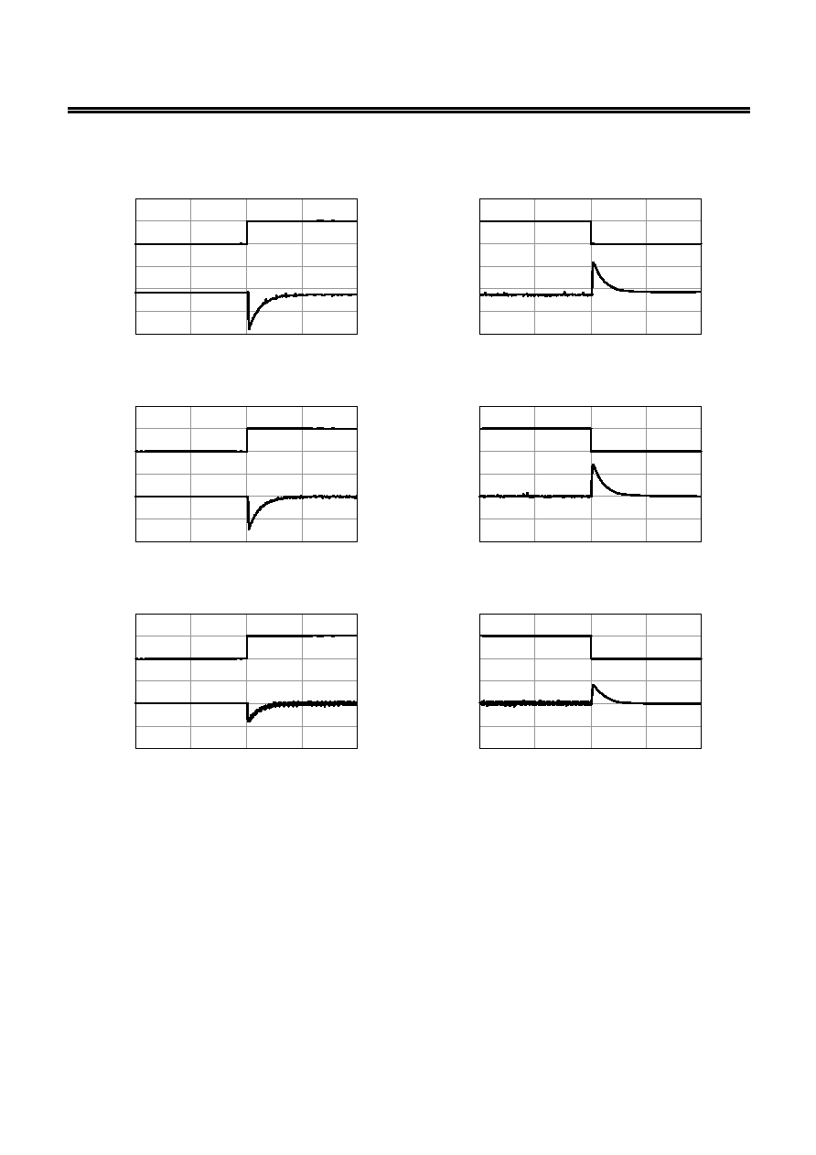
3. Load fluctuations (V
OUT
=
=
=
= 9.2 V, V
IN
=
=
=
= 3.3 V, Ta ==== 25įįįįC, R
Z
= 200 k
, C
Z
= 0.01
Ķ
Ķ
Ķ
ĶF)
3-1. f
OSC
= 1133 kHz, I
OUT
= 0.1 mA100 mA
3-2. f
OSC
= 1133 kHz, I
OUT
= 100 mA0.1 mA
≠20 ≠10 0 10 20
time [ms]
8.8
9.0
V
OUT
[0.2 V/div]
9.2
I
OUT
100 mA
0.1 mA
9.4
9.6
9.8
10.0
≠20 ≠10 0 10 20
time [ms]
8.8
9.0
V
OUT
[0.2 V/div]
9.2
I
OUT
100 mA
0.1 mA
9.4
9.6
9.8
10.0
3-3. f
OSC
= 700 kHz, I
OUT
= 0.1 mA100 mA
3-4. f
OSC
= 700 kHz, I
OUT
= 100 mA0.1 mA
≠20 ≠10 0 10 20
time [ms]
8.8
9.0
V
OUT
[0.2 V/div]
9.2
I
OUT
100 mA
0.1 mA
9.4
9.6
9.8
10.0
≠20 ≠10 0 10 20
time [ms]
8.8
9.0
V
OUT
[0.2 V/div]
9.2
I
OUT
100 mA
0.1 mA
9.4
9.6
9.8
10.0
3-5. f
OSC
= 286 kHz, I
OUT
= 0.1 mA100 mA
3-6. f
OSC
= 286 kHz, I
OUT
= 100 mA0.1 mA
≠20 ≠10 0 10 20
time [ms]
8.8
9.0
V
OUT
[0.2 V/div]
9.2
I
OUT
100 mA
0.1 mA
9.4
9.6
9.8
10.0
≠20 ≠10 0 10 20
time [ms]
8.8
9.0
V
OUT
[0.2 V/div]
9.2
I
OUT
100 mA
0.1 mA
9.4
9.6
9.8
10.0
STEP-UP, HIGH-FREQUENCY, PWM CONTROL SWITCHING REGULATOR CONTROLLERS
S-8337/8338 Series
Rev.2.0
_00
32
Seiko Instruments Inc.
4. Input voltage fluctuations (V
OUT
=
=
=
= 9.2 V, I
OUT
=
=
=
= 100 mA, R
Z
= 200 k
, C
Z
= 0.01
Ķ
Ķ
Ķ
ĶF)
4-1. f
OSC
= 1133 kHz, V
IN
= 2.7 V3.7 V
4-2. f
OSC
= 1133 kHz, V
IN
= 3.7 V2.7 V
≠20 ≠10 0 10 20
time [ms]
9.15
V
OUT
[V]
9.20
V
IN
[V]
4.0
3.5
3.0
2.5
9.25
9.30
≠20 ≠10 0 10 20
time [ms]
9.15
V
OUT
[V]
9.20
V
IN
[V]
4.0
3.5
3.0
2.5
9.25
9.30
4-3. f
OSC
= 700 kHz, V
IN
= 2.7 V3.7 V
4-4. f
OSC
= 700 kHz, V
IN
= 3.7 V2.7 V
≠20 ≠10 0 10 20
time [ms]
9.15
V
OUT
[V]
9.20
V
IN
[V]
4.0
3.5
3.0
2.5
9.25
9.30
≠20 ≠10 0 10 20
time [ms]
9.15
V
OUT
[V]
9.20
V
IN
[V]
4.0
3.5
3.0
2.5
9.25
9.30
4-5. f
OSC
= 286 kHz, V
IN
= 2.7 V3.7 V
4-6. f
OSC
= 286 kHz, V
IN
= 3.7 V2.7 V
≠20 ≠10 0 10 20
time [ms]
9.15
V
OUT
[V]
9.20
V
IN
[V]
4.0
3.5
3.0
2.5
9.25
9.30
≠20 ≠10 0 10 20
time [ms]
9.15
V
OUT
[V]
9.20
V
IN
[V]
4.0
3.5
3.0
2.5
9.25
9.30
STEP-UP, HIGH-FREQUENCY, PWM CONTROL SWITCHING REGULATOR CONTROLLERS
Rev.2.0
_00
S-8337/8338 Series
Seiko Instruments Inc.
33
Reference Data
1. Reference data for external parts
Table 8 Properties of External Parts
Element Name
Product Name
Manufacture
Characteristics
Inductor LDR655312T
TDK Corporation
4.7
ĶH, DCR
*1
= 206 m
, I
MAX
*2
= 0.9 A,
Height = 1.2 mm
Diode RB491D
Rohm Co., Ltd.
V
F
*3
= 0.45 V, I
F
*4
= 1.0 A
Output capacitor
16
V,
10
ĶF
Transistor MCH3406
Sanyo Electric Co., Ltd.
V
DSS
*5
= 20 V, V
GSS
*6
=
Ī10 V, C
iss
*7
= 280 pF,
R
DS(ON)
*8
= 82 m
max. (V
GS
*9
= 2.5 V, I
D
*10
= 1 A)
*1. DCR :
DC resistance
*2. I
MAX
:
Maximum allowable current
*3. V
F
:
Forward voltage
*4. I
F
:
Forward current
*5. V
DSS
:
Drain to source voltage (When between gate and source short circuits)
*6. V
GSS
:
Gate to source voltage (When between drain and source short circuits)
*7. C
iss
:
Input capacitance
*8. R
DS(ON)
:
Drain to source on resistance
*9. V
GS
:
Gate to source voltage
*10. I
D
:
Drain current
Caution The values shown in the characteristics column of Table 8 above are based on the
materials provided by each manufacturer. However, consider the characteristics of the
original materials when using the above products.

STEP-UP, HIGH-FREQUENCY, PWM CONTROL SWITCHING REGULATOR CONTROLLERS
S-8337/8338 Series
Rev.2.0
_00
34
Seiko Instruments Inc.
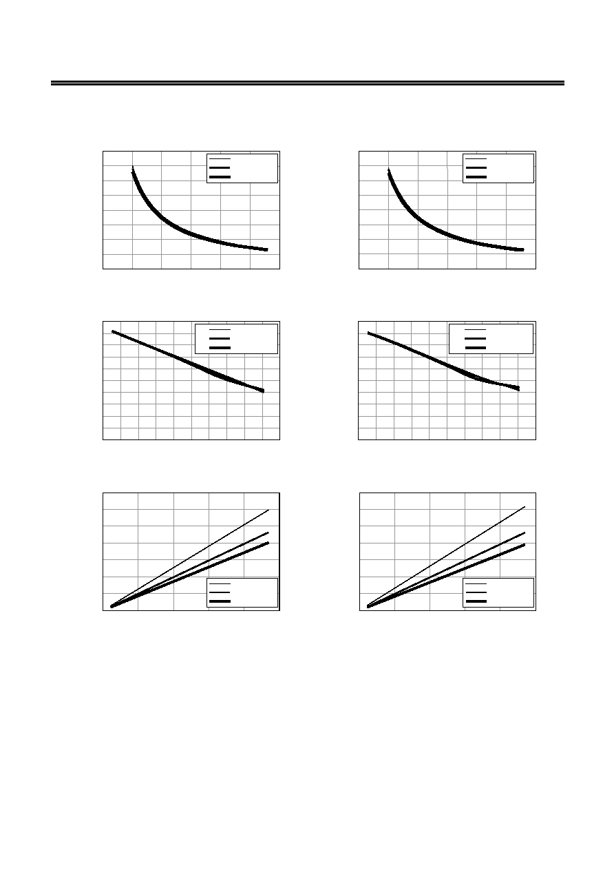
2. Reference data (1)
The data of (a) output current (I
OUT
) vs. efficiency (
) characteristics and (b) output current (I
OUT
) vs.
output voltage (V
OUT
) characteristics is shown below.
2-1. V
OUT
=
=
=
= 13.1 V (R
FB1
=
=
=
= 7.5 k
, R
FB2
=
=
=
= 620
)
(1) f
OSC
= 1133 kHz, MaxDuty = 77 % (R
OSC
= 120 k, R
Duty
= 180 k)
(a) I
OUT
vs.
(b)
I
OUT
vs. V
OUT
100
90
80
70
60
50
40
30
20
10
0
1 10 100
1000
0.1
[%]
I
OUT
[mA]
0.01
V
IN
= 5.0 V
13.20
13.15
13.10
13.05
13.00
12.95
12.90
V
OUT
[V]
1 10 100
1000
0.1
I
OUT
[mA]
0.01
V
IN
= 5.0 V
(2) f
OSC
= 700 kHz, MaxDuty = 77 % (R
OSC
= 200 k, R
Duty
= 300 k)
(a) I
OUT
vs.
(b)
I
OUT
vs. V
OUT
100
90
80
70
60
50
40
30
20
10
0
1 10 100
1000
0.1
[%]
I
OUT
[mA]
0.01
V
IN
= 5.0 V
13.20
13.15
13.10
13.05
13.00
12.95
12.90
V
OUT
[V]
1 10 100
1000
0.1
I
OUT
[mA]
0.01
V
IN
= 5.0 V
(3) f
OSC
= 286 kHz, MaxDuty = 77 % (R
OSC
= 510 k, R
Duty
= 750 k)
(a) I
OUT
vs.
(b)
I
OUT
vs. V
OUT
100
90
80
70
60
50
40
30
20
10
0
1 10 100
1000
0.1
[%]
I
OUT
[mA]
0.01
V
IN
= 5.0 V
13.20
13.15
13.10
13.05
13.00
12.95
12.90
V
OUT
[V]
1 10 100
1000
0.1
I
OUT
[mA]
0.01
V
IN
= 5.0 V

STEP-UP, HIGH-FREQUENCY, PWM CONTROL SWITCHING REGULATOR CONTROLLERS
Rev.2.0
_00
S-8337/8338 Series
Seiko Instruments Inc.
35
2-2. V
OUT
=
=
=
= 9.2 V (R
FB1
=
=
=
= 8.2 k
, R
FB2
=
=
=
= 1.0 k
)
(1) f
OSC
= 1133 kHz, MaxDuty = 77 % (R
OSC
= 120 k, R
Duty
= 180 k)
(a) I
OUT
vs.
(b)
I
OUT
vs. V
OUT
100
90
80
70
60
50
40
30
20
10
0
1 10 100
1000
0.1
[%]
I
OUT
[mA]
0.01
V
IN
= 5.0 V
V
IN
= 3.3 V
9.30
9.25
9.20
9.15
9.10
9.05
9.00
V
OUT
[V]
1 10 100
1000
0.1
I
OUT
[mA]
0.01
V
IN
= 5.0 V
V
IN
= 3.3 V
(2) f
OSC
= 700 kHz, MaxDuty = 77 % (R
OSC
= 200 k, R
Duty
= 300 k)
(a) I
OUT
vs.
(b)
I
OUT
vs. V
OUT
100
90
80
70
60
50
40
30
20
10
0
1 10 100
1000
0.1
[%]
I
OUT
[mA]
0.01
V
IN
= 5.0 V
V
IN
= 3.3 V
9.30
9.25
9.20
9.15
9.10
9.05
9.00
V
OUT
[V]
1 10 100
1000
0.1
I
OUT
[mA]
0.01
V
IN
= 5.0 V
V
IN
= 3.3 V
(3) f
OSC
= 286 kHz, MaxDuty = 77 % (R
OSC
= 510 k, R
Duty
= 750 k)
(a) I
OUT
vs.
(b)
I
OUT
vs. V
OUT
100
90
80
70
60
50
40
30
20
10
0
1 10 100
1000
0.1
[%]
I
OUT
[mA]
0.01
V
IN
= 5.0 V
V
IN
= 3.3 V
9.30
9.25
9.20
9.15
9.10
9.05
9.00
V
OUT
[V]
1 10 100
1000
0.1
I
OUT
[mA]
0.01
V
IN
= 5.0 V
V
IN
= 3.3 V
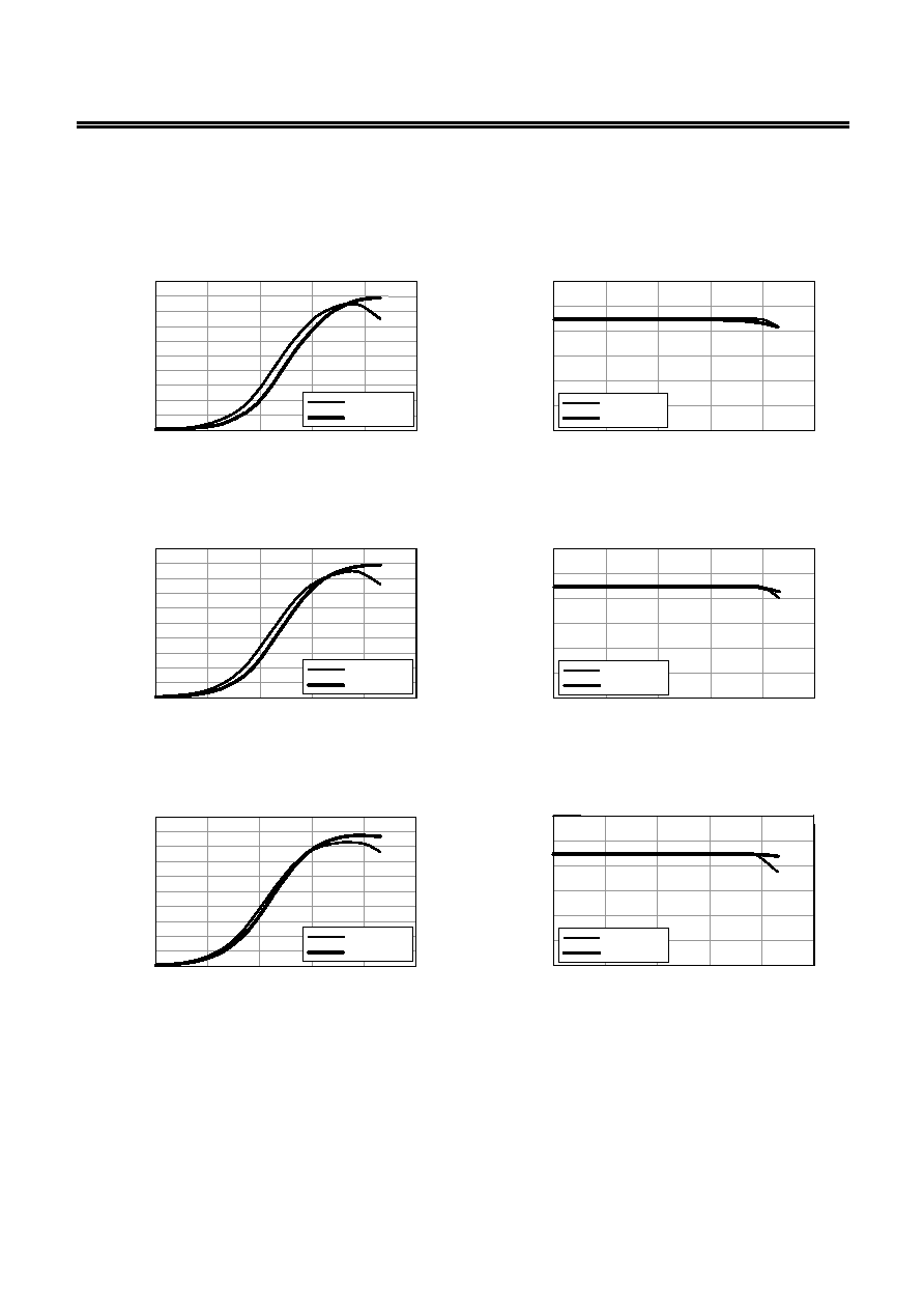
STEP-UP, HIGH-FREQUENCY, PWM CONTROL SWITCHING REGULATOR CONTROLLERS
S-8337/8338 Series
Rev.2.0
_00
36
Seiko Instruments Inc.
2-3. V
OUT
=
=
=
= 6.1 V (R
FB1
=
=
=
= 5.1 k
, R
FB2
=
=
=
= 1.0 k
)
(1) f
OSC
= 1133 kHz, MaxDuty = 77 % (R
OSC
= 120 k, R
Duty
= 180 k)
(a) I
OUT
vs.
(b)
I
OUT
vs. V
OUT
100
90
80
70
60
50
40
30
20
10
0
1 10 100
1000
0.1
[%]
I
OUT
[mA]
0.01
V
IN
= 3.3 V
V
IN
= 1.8 V
6.20
6.15
6.10
6.05
6.00
5.95
5.90
V
OUT
[V]
1 10 100
1000
0.1
I
OUT
[mA]
0.01
V
IN
= 3.3 V
V
IN
= 1.8 V
(2) f
OSC
= 700 kHz, MaxDuty = 77 % (R
OSC
= 200 k, R
Duty
= 300 k)
(a) I
OUT
vs.
(b)
I
OUT
vs. V
OUT
100
90
80
70
60
50
40
30
20
10
0
1 10 100
1000
0.1
[%]
I
OUT
[mA]
0.01
V
IN
= 3.3 V
V
IN
= 1.8 V
6.20
6.15
6.10
6.05
6.00
5.95
5.90
V
OUT
[V]
1 10 100
1000
0.1
I
OUT
[mA]
0.01
V
IN
= 3.3 V
V
IN
= 1.8 V
(3) f
OSC
= 286 kHz, MaxDuty = 77 % (R
OSC
= 510 k, R
Duty
= 750 k)
(a) I
OUT
vs.
(b)
I
OUT
vs. V
OUT
100
90
80
70
60
50
40
30
20
10
0
1 10 100
1000
0.1
[%]
I
OUT
[mA]
0.01
V
IN
= 3.3 V
V
IN
= 1.8 V
6.20
6.15
6.10
6.05
6.00
5.95
5.90
V
OUT
[V]
1 10 100
1000
0.1
I
OUT
[mA]
0.01
V
IN
= 3.3 V
V
IN
= 1.8 V
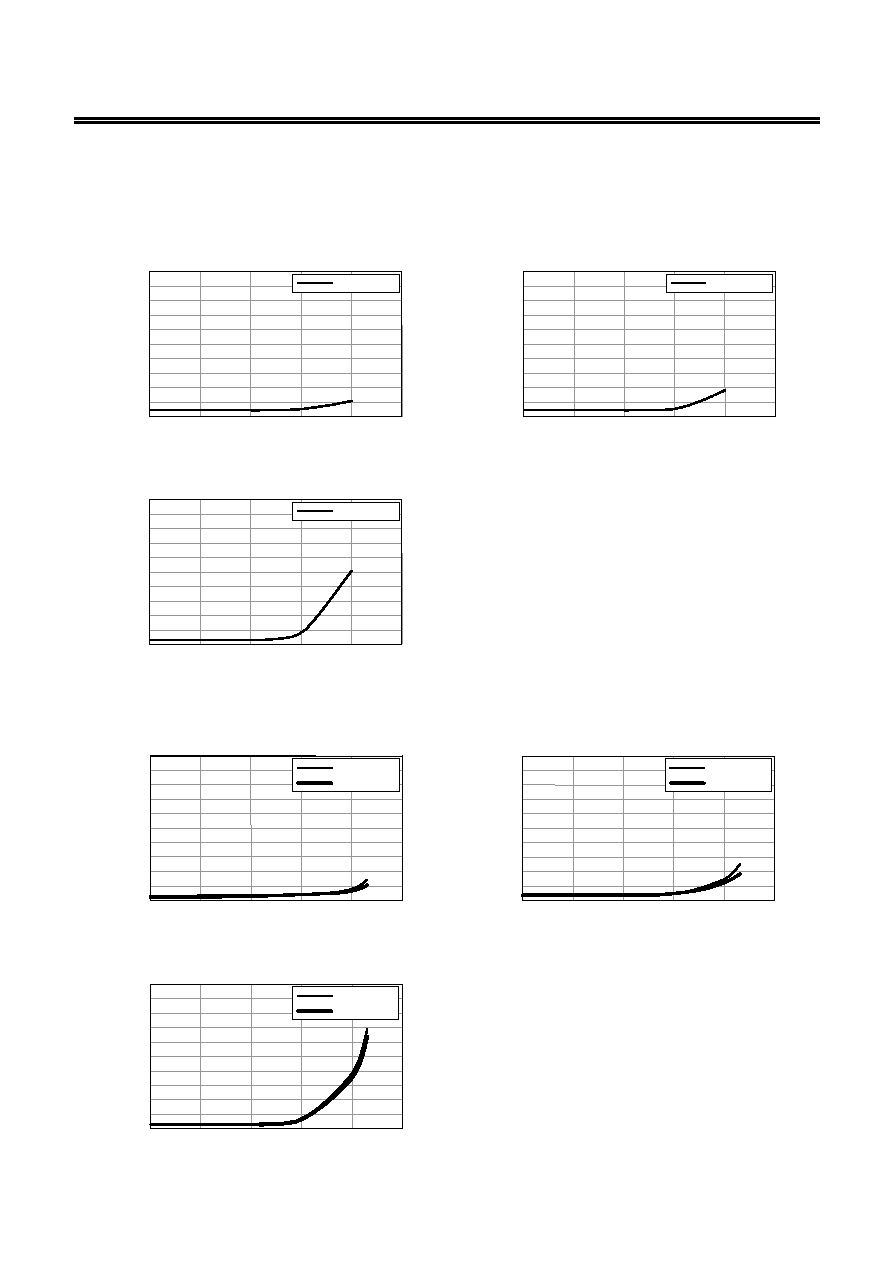
STEP-UP, HIGH-FREQUENCY, PWM CONTROL SWITCHING REGULATOR CONTROLLERS
Rev.2.0
_00
S-8337/8338 Series
Seiko Instruments Inc.
37
3. Reference data (2)
The data of output current (I
OUT
) vs. ripple voltage (Vr) characteristics is shown below.
3-1. V
OUT
=
=
=
= 13.1 V (R
FB1
=
=
=
= 7.5 k
, R
FB2
=
=
=
= 620
)
(1) f
OSC
= 1133 kHz, MaxDuty = 77 % (R
OSC
= 120 k, R
Duty
= 180 k) (2)
f
OSC
= 700 kHz, MaxDuty = 77 % (R
OSC
= 200 k, R
Duty
= 300 k)
100
90
80
70
60
50
40
30
20
10
0
1 10 100
1000
0.1
Vr
[mV]
I
OUT
[mA]
0.01
V
IN
= 5.0 V
100
90
80
70
60
50
40
30
20
10
0
1 10 100
1000
0.1
Vr
[mV]
I
OUT
[mA]
0.01
V
IN
= 5.0 V
(3) f
OSC
= 286 kHz, MaxDuty = 77 % (R
OSC
= 510 k, R
Duty
= 750 k)
100
90
80
70
60
50
40
30
20
10
0
1 10 100
1000
0.1
Vr
[mV]
I
OUT
[mA]
0.01
V
IN
= 5.0 V
3-2. V
OUT
=
=
=
= 9.2 V (R
FB1
=
=
=
= 8.2 k
, R
FB2
=
=
=
= 1.0 k
)
(1) f
OSC
= 1133 kHz, MaxDuty = 77 % (R
OSC
= 120 k, R
Duty
= 180 k) (2)
f
OSC
= 700 kHz, MaxDuty = 77 % (R
OSC
= 200 k, R
Duty
= 300 k)
100
90
80
70
60
50
40
30
20
10
0
1 10 100
1000
0.1
Vr
[mV]
I
OUT
[mA]
0.01
V
IN
= 5.0 V
V
IN
= 3.3 V
100
90
80
70
60
50
40
30
20
10
0
1 10 100
1000
0.1
Vr
[mV]
I
OUT
[mA]
0.01
V
IN
= 5.0 V
V
IN
= 3.3 V
(3) f
OSC
= 286 kHz, MaxDuty = 77 % (R
OSC
= 510 k, R
Duty
= 750 k)
100
90
80
70
60
50
40
30
20
10
0
1 10 100
1000
0.1
Vr
[mV]
I
OUT
[mA]
0.01
V
IN
= 5.0 V
V
IN
= 3.3 V
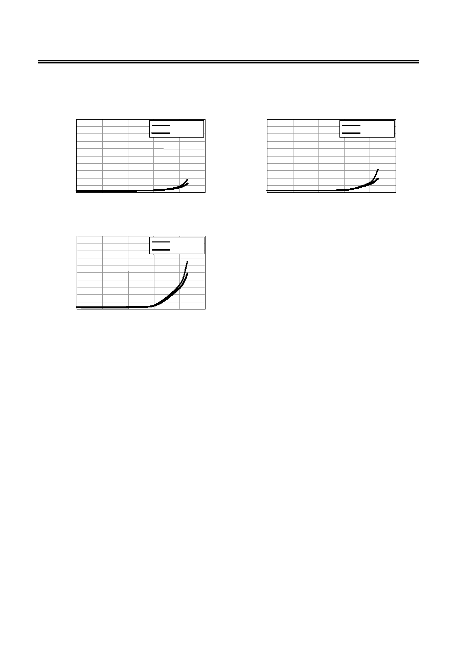
STEP-UP, HIGH-FREQUENCY, PWM CONTROL SWITCHING REGULATOR CONTROLLERS
S-8337/8338 Series
Rev.2.0
_00
38
Seiko Instruments Inc.
3-3. V
OUT
=
=
=
= 6.1 V (R
FB1
=
=
=
= 5.1 k
, R
FB2
=
=
=
= 1.0 k
)
(1) f
OSC
= 1133 kHz, MaxDuty = 77 % (R
OSC
= 120 k, R
Duty
= 180 k) (2)
f
OSC
= 700 kHz, MaxDuty = 77 % (R
OSC
= 200 k, R
Duty
= 300 k)
100
90
80
70
60
50
40
30
20
10
0
1 10 100
1000
0.1
Vr
[mV]
I
OUT
[mA]
0.01
V
IN
= 3.3 V
V
IN
= 1.8 V
100
90
80
70
60
50
40
30
20
10
0
1 10 100
1000
0.1
Vr
[mV]
I
OUT
[mA]
0.01
V
IN
= 3.3 V
V
IN
= 1.8 V
(3) f
OSC
= 286 kHz, MaxDuty = 77 % (R
OSC
= 510 k, R
Duty
= 750 k)
100
90
80
70
60
50
40
30
20
10
0
1 10 100
1000
0.1
Vr
[mV]
I
OUT
[mA]
0.01
V
IN
= 3.3 V
V
IN
= 1.8 V
STEP-UP, HIGH-FREQUENCY, PWM CONTROL SWITCHING REGULATOR CONTROLLERS
Rev.2.0
_00
S-8337/8338 Series
Seiko Instruments Inc.
39
Marking Specification
(1) 8-Pin SON(A)
(1) ~ (3) Product code (Refer to Product name vs. Product code)
(4) ~ (8) Lot number
8-Pin SON(A)
Top view
8
5
(1) (2) (3)
(5) (6) (7)
(4)
(8)
1
2
Product name vs. Product code
(a) S-8337Series
Product code
Product code
Product name
(1) (2) (3)
Product name
(1) (2) (3)
S-8337AAAA-P8T1 O
B
A
S-8337ABEC-P8T1 O
D
N
S-8337AAAB-P8T1
O B B
S-8337ABFA-P8T1
O D O
S-8337AAAC-P8T1
O B 2
S-8337ABFB-P8T1
O D P
S-8337AABA-P8T1
O B C
S-8337ABFC-P8T1
O D Q
S-8337AABB-P8T1 O
B
D
S-8337ABGA-P8T1 O
D
R
S-8337AABC-P8T1
O B E
S-8337ABGB-P8T1
O D S
S-8337AACA-P8T1 O
B
F
S-8337ABGC-P8T1 O
D
T
S-8337AACB-P8T1
O B G
S-8337ABHA-P8T1
O D U
S-8337AACC-P8T1
O B H
S-8337ABHB-P8T1
O D V
S-8337AADA-P8T1 O
B
I
S-8337ABHC-P8T1 O
D
W
S-8337AADB-P8T1 O
B
J
S-8337ABIA-P8T1 O
D
X
S-8337AADC-P8T1 O
B
K
S-8337ABIB-P8T1 O
D
Y
S-8337AAEA-P8T1 O
B
L
S-8337ABIC-P8T1 O
D
Z
S-8337AAEB-P8T1 O
B
M
S-8337ACAA-P8T1 O
J
A
S-8337AAEC-P8T1 O
B
N
S-8337ACAB-P8T1 O
J
B
S-8337AAFA-P8T1
O B O
S-8337ACAC-P8T1
O J 2
S-8337AAFB-P8T1
O B P
S-8337ACBA-P8T1
O J C
S-8337AAFC-P8T1
O B Q
S-8337ACBB-P8T1
O J D
S-8337AAGA-P8T1 O
B
R
S-8337ACBC-P8T1 O
J
E
S-8337AAGB-P8T1
O B S
S-8337ACCA-P8T1
O J F
S-8337AAGC-P8T1
O B T
S-8337ACCB-P8T1
O J G
S-8337AAHA-P8T1 O
B
U
S-8337ACCC-P8T1 O
J
H
S-8337AAHB-P8T1
O B V
S-8337ACDA-P8T1
O J I
S-8337AAHC-P8T1 O
B
W
S-8337ACDB-P8T1 O
J
J
S-8337AAIA-P8T1 O
B
X
S-8337ACDC-P8T1
O
J
K
S-8337AAIB-P8T1 O
B
Y
S-8337ACEA-P8T1 O
J
L
S-8337AAIC-P8T1 O
B
Z
S-8337ACEB-P8T1 O
J
M
S-8337ABAA-P8T1 O
D
A
S-8337ACEC-P8T1 O
J
N
S-8337ABAB-P8T1
O D B
S-8337ACFA-P8T1
O J O
S-8337ABAC-P8T1 O
D
2
S-8337ACFB-P8T1 O
J
P
S-8337ABBA-P8T1
O D C
S-8337ACFC-P8T1
O J Q
S-8337ABBB-P8T1 O
D
D
S-8337ACGA-P8T1 O
J
R
S-8337ABBC-P8T1 O
D
E
S-8337ACGB-P8T1 O
J
S
S-8337ABCA-P8T1
O D F
S-8337ACGC-P8T1
O J T
S-8337ABCB-P8T1
O D G
S-8337ACHA-P8T1
O J U
S-8337ABCC-P8T1 O
D
H
S-8337ACHB-P8T1 O
J
V
S-8337ABDA-P8T1 O
D
I
S-8337ACHC-P8T1 O
J
W
S-8337ABDB-P8T1 O
D
J
S-8337ACIA-P8T1 O
J
X
S-8337ABDC-P8T1 O
D
K
S-8337ACIB-P8T1 O
J
Y
S-8337ABEA-P8T1 O
D
L
S-8337ACIC-P8T1 O
J
Z
S-8337ABEB-P8T1
O
D
M

STEP-UP, HIGH-FREQUENCY, PWM CONTROL SWITCHING REGULATOR CONTROLLERS
S-8337/8338 Series
Rev.2.0
_00
40
Seiko Instruments Inc.
(b) S-8338 Series
Product code
Product code
Product name
(1) (2) (3)
Product name
(1) (2) (3)
S-8338AAAA-P8T1 O
C
A
S-8338ABEC-P8T1 O
I
N
S-8338AAAB-P8T1 O
C
B
S-8338ABFA-P8T1 O
I
O
S-8338AAAC-P8T1 O
C
2
S-8338ABFB-P8T1 O
I
P
S-8338AABA-P8T1 O
C
C
S-8338ABFC-P8T1 O
I
Q
S-8338AABB-P8T1 O
C
D
S-8338ABGA-P8T1 O
I
R
S-8338AABC-P8T1 O
C
E
S-8338ABGB-P8T1 O
I
S
S-8338AACA-P8T1 O
C
F
S-8338ABGC-P8T1 O
I
T
S-8338AACB-P8T1
O C G
S-8338ABHA-P8T1
O I U
S-8338AACC-P8T1 O
C
H
S-8338ABHB-P8T1 O
I
V
S-8338AADA-P8T1 O
C
I
S-8338ABHC-P8T1 O
I
W
S-8338AADB-P8T1 O
C
J
S-8338ABIA-P8T1 O
I
X
S-8338AADC-P8T1 O
C
K
S-8338ABIB-P8T1 O
I
Y
S-8338AAEA-P8T1 O
C
L
S-8338ABIC-P8T1 O
I
Z
S-8338AAEB-P8T1
O C M
S-8338ACAA-P8T1
O K A
S-8338AAEC-P8T1
O C N
S-8338ACAB-P8T1
O K B
S-8338AAFA-P8T1
O C O
S-8338ACAC-P8T1
O K 2
S-8338AAFB-P8T1
O C P
S-8338ACBA-P8T1
O K C
S-8338AAFC-P8T1
O C Q
S-8338ACBB-P8T1
O K D
S-8338AAGA-P8T1
O C R
S-8338ACBC-P8T1
O K E
S-8338AAGB-P8T1
O C S
S-8338ACCA-P8T1
O K F
S-8338AAGC-P8T1
O C T
S-8338ACCB-P8T1
O K G
S-8338AAHA-P8T1
O C U
S-8338ACCC-P8T1
O K H
S-8338AAHB-P8T1
O C V
S-8338ACDA-P8T1
O K I
S-8338AAHC-P8T1
O C W
S-8338ACDB-P8T1
O K J
S-8338AAIA-P8T1
O C X
S-8338ACDC-P8T1
O K K
S-8338AAIB-P8T1
O C Y
S-8338ACEA-P8T1
O K L
S-8338AAIC-P8T1
O C Z
S-8338ACEB-P8T1
O K M
S-8338ABAA-P8T1 O
I
A
S-8338ACEC-P8T1 O
K
N
S-8338ABAB-P8T1
O I B
S-8338ACFA-P8T1
O K O
S-8338ABAC-P8T1 O
I
2
S-8338ACFB-P8T1 O
K
P
S-8338ABBA-P8T1
O I C
S-8338ACFC-P8T1
O K Q
S-8338ABBB-P8T1 O
I
D
S-8338ACGA-P8T1 O
K
R
S-8338ABBC-P8T1 O
I
E
S-8338ACGB-P8T1 O
K
S
S-8338ABCA-P8T1 O
I
F
S-8338ACGC-P8T1 O
K
T
S-8338ABCB-P8T1 O
I
G
S-8338ACHA-P8T1 O
K
U
S-8338ABCC-P8T1 O
I
H
S-8338ACHB-P8T1 O
K
V
S-8338ABDA-P8T1 O
I
I
S-8338ACHC-P8T1 O
K
W
S-8338ABDB-P8T1 O
I
J
S-8338ACIA-P8T1 O
K
X
S-8338ABDC-P8T1 O
I
K
S-8338ACIB-P8T1 O
K
Y
S-8338ABEA-P8T1 O
I
L
S-8338ACIC-P8T1 O
K
Z
S-8338ABEB-P8T1
O I M
STEP-UP, HIGH-FREQUENCY, PWM CONTROL SWITCHING REGULATOR CONTROLLERS
Rev.2.0
_00
S-8337/8338 Series
Seiko Instruments Inc.
41
(2) 8-Pin TSSOP
(1) ~ (4)
Product name: 8337 or 8338 (Fixed)
8337 indicates S-8337 series.
8338 indicates S-8338 series.
(5) ~ (8)
Function code (Refer to Product name vs. Function code)
(9) ~ (14) Lot number
8-Pin TSSOP
Top view
(1) (2) (3) (4)
(5) (6) (7) (8)
(11) (12) (13) (14)
(9) (10)
1
4
8
5
Product name vs. Function code
(a) S-8337 Series
Function code
Function code
Product name
(5) (6) (7) (8)
Product name
(5) (6) (7) (8)
S-8337AAAA-T8T1
A A A A S-8337ABEC-T8T1
A B E C
S-8337AAAB-T8T1
A A A B S-8337ABFA-T8T1
A B F A
S-8337AAAC-T8T1 A
A
A
C
S-8337ABFB-T8T1 A
B
F
B
S-8337AABA-T8T1
A A B A S-8337ABFC-T8T1
A B F C
S-8337AABB-T8T1
A A B B S-8337ABGA-T8T1
A B G A
S-8337AABC-T8T1
A A B C S-8337ABGB-T8T1
A B G B
S-8337AACA-T8T1
A A C A S-8337ABGC-T8T1
A B G C
S-8337AACB-T8T1
A A C B S-8337ABHA-T8T1
A B H A
S-8337AACC-T8T1
A A C C S-8337ABHB-T8T1
A B H B
S-8337AADA-T8T1
A A D A S-8337ABHC-T8T1
A B H C
S-8337AADB-T8T1
A A D B S-8337ABIA-T8T1
A B I A
S-8337AADC-T8T1
A A D C S-8337ABIB-T8T1
A B I B
S-8337AAEA-T8T1
A A E A S-8337ABIC-T8T1
A B I C
S-8337AAEB-T8T1
A A E B S-8337ACAA-T8T1
A C A A
S-8337AAEC-T8T1
A A E C S-8337ACAB-T8T1
A C A B
S-8337AAFA-T8T1
A A F A S-8337ACAC-T8T1
A C A C
S-8337AAFB-T8T1
A A F B S-8337ACBA-T8T1
A C B A
S-8337AAFC-T8T1
A A F C S-8337ACBB-T8T1
A C B B
S-8337AAGA-T8T1
A A G A S-8337ACBC-T8T1
A C B C
S-8337AAGB-T8T1
A A G B S-8337ACCA-T8T1
A C C A
S-8337AAGC-T8T1
A A G C S-8337ACCB-T8T1
A C C B
S-8337AAHA-T8T1
A A H A S-8337ACCC-T8T1
A C C C
S-8337AAHB-T8T1
A A H B S-8337ACDA-T8T1
A C D A
S-8337AAHC-T8T1
A A H C S-8337ACDB-T8T1
A C D B
S-8337AAIA-T8T1
A A I A S-8337ACDC-T8T1
A C D C
S-8337AAIB-T8T1
A A I B S-8337ACEA-T8T1
A C E A
S-8337AAIC-T8T1
A A I C S-8337ACEB-T8T1
A C E B
S-8337ABAA-T8T1
A B A A S-8337ACEC-T8T1
A C E C
S-8337ABAB-T8T1
A B A B S-8337ACFA-T8T1
A C F A
S-8337ABAC-T8T1
A B A C S-8337ACFB-T8T1
A C F B
S-8337ABBA-T8T1
A B B A S-8337ACFC-T8T1
A C F C
S-8337ABBB-T8T1
A B B B S-8337ACGA-T8T1
A C G A
S-8337ABBC-T8T1
A B B C S-8337ACGB-T8T1
A C G B
S-8337ABCA-T8T1
A B C A S-8337ACGC-T8T1
A C G C
S-8337ABCB-T8T1
A B C B S-8337ACHA-T8T1
A C H A
S-8337ABCC-T8T1
A B C C S-8337ACHB-T8T1
A C H B
S-8337ABDA-T8T1
A B D A S-8337ACHC-T8T1
A C H C
S-8337ABDB-T8T1
A B D B S-8337ACIA-T8T1
A C I A
S-8337ABDC-T8T1
A B D C S-8337ACIB-T8T1
A C I B
S-8337ABEA-T8T1
A B E A S-8337ACIC-T8T1
A C I C
S-8337ABEB-T8T1
A B E B
STEP-UP, HIGH-FREQUENCY, PWM CONTROL SWITCHING REGULATOR CONTROLLERS
S-8337/8338 Series
Rev.2.0
_00
42
Seiko Instruments Inc.
(b) S-8338 Series
Function code
Function code
Product name
(5) (6) (7) (8)
Product name
(5) (6) (7) (8)
S-8338AAAA-T8T1
A A A A S-8338ABEC-T8T1
A B E C
S-8338AAAB-T8T1
A A A B S-8338ABFA-T8T1
A B F A
S-8338AAAC-T8T1 A
A
A
C
S-8338ABFB-T8T1 A
B
F
B
S-8338AABA-T8T1
A A B A S-8338ABFC-T8T1
A B F C
S-8338AABB-T8T1
A A B B S-8338ABGA-T8T1
A B G A
S-8338AABC-T8T1
A A B C S-8338ABGB-T8T1
A B G B
S-8338AACA-T8T1
A A C A S-8338ABGC-T8T1
A B G C
S-8338AACB-T8T1
A A C B S-8338ABHA-T8T1
A B H A
S-8338AACC-T8T1
A A C C S-8338ABHB-T8T1
A B H B
S-8338AADA-T8T1
A A D A S-8338ABHC-T8T1
A B H C
S-8338AADB-T8T1
A A D B S-8338ABIA-T8T1
A B I A
S-8338AADC-T8T1
A A D C S-8338ABIB-T8T1
A B I B
S-8338AAEA-T8T1
A A E A S-8338ABIC-T8T1
A B I C
S-8338AAEB-T8T1
A A E B S-8338ACAA-T8T1
A C A A
S-8338AAEC-T8T1
A A E C S-8338ACAB-T8T1
A C A B
S-8338AAFA-T8T1
A A F A S-8338ACAC-T8T1
A C A C
S-8338AAFB-T8T1
A A F B S-8338ACBA-T8T1
A C B A
S-8338AAFC-T8T1
A A F C S-8338ACBB-T8T1
A C B B
S-8338AAGA-T8T1
A A G A S-8338ACBC-T8T1
A C B C
S-8338AAGB-T8T1
A A G B S-8338ACCA-T8T1
A C C A
S-8338AAGC-T8T1
A A G C S-8338ACCB-T8T1
A C C B
S-8338AAHA-T8T1
A A H A S-8338ACCC-T8T1
A C C C
S-8338AAHB-T8T1
A A H B S-8338ACDA-T8T1
A C D A
S-8338AAHC-T8T1
A A H C S-8338ACDB-T8T1
A C D B
S-8338AAIA-T8T1 A
A
I
A
S-8338ACDC-T8T1
A
C
D
C
S-8338AAIB-T8T1
A A I B S-8338ACEA-T8T1
A C E A
S-8338AAIC-T8T1
A A I C S-8338ACEB-T8T1
A C E B
S-8338ABAA-T8T1
A B A A S-8338ACEC-T8T1
A C E C
S-8338ABAB-T8T1
A B A B S-8338ACFA-T8T1
A C F A
S-8338ABAC-T8T1 A
B
A
C
S-8338ACFB-T8T1 A
C
F
B
S-8338ABBA-T8T1
A B B A S-8338ACFC-T8T1
A C F C
S-8338ABBB-T8T1
A B B B S-8338ACGA-T8T1
A C G A
S-8338ABBC-T8T1
A B B C S-8338ACGB-T8T1
A C G B
S-8338ABCA-T8T1
A B C A S-8338ACGC-T8T1
A C G C
S-8338ABCB-T8T1
A B C B S-8338ACHA-T8T1
A C H A
S-8338ABCC-T8T1
A B C C S-8338ACHB-T8T1
A C H B
S-8338ABDA-T8T1
A B D A S-8338ACHC-T8T1
A C H C
S-8338ABDB-T8T1 A
B
D
B
S-8338ACIA-T8T1 A
C
I
A
S-8338ABDC-T8T1 A
B
D
C
S-8338ACIB-T8T1 A
C
I
B
S-8338ABEA-T8T1
A B E A S-8338ACIC-T8T1
A C I C
S-8338ABEB-T8T1
A B E B

2.90Ī0.2
8
5
0.475typ.
1
4
0.30
0.65
+0.1
-0.05
(Ý1.0)
(2.3)
No.
TITLE
SCALE
UNIT
mm
Seiko Instruments Inc.
No. PN008-A-P-SD-1.1
PN008-A-P-SD-1.1
SON8A-A-PKG Dimensions
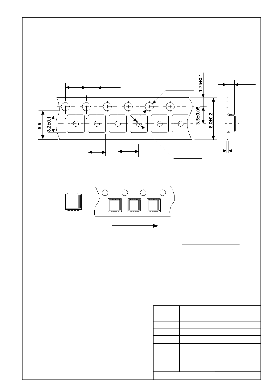
Ý1.05Ī0.05
0.2Ī0.05
1.5Ī0.1
Ý1.55Ī0.05
2.0Ī0.05
4.0Ī0.1
3.3Ī0.1
4.0Ī0.1
No.
TITLE
SCALE
UNIT
mm
1
4
5
8
Seiko Instruments Inc.
No. PN008-A-C-SD-1.1
PN008-A-C-SD-1.1
SON8A-A-Carrier Tape
Feed direction
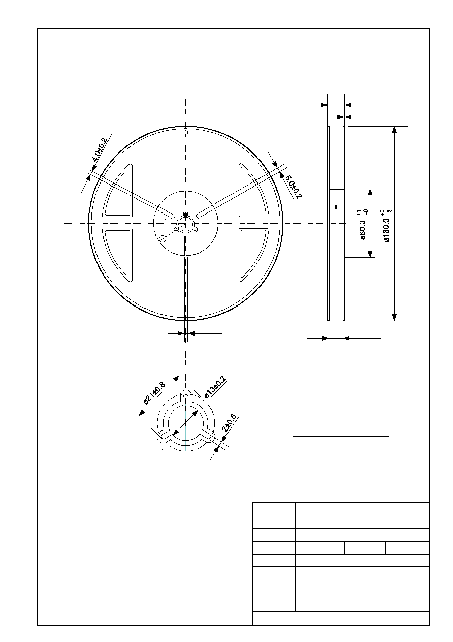
(1.2)
9.0Ī0.3
No.
TITLE
SCALE
UNIT
mm
QTY.
3000
3.0Ī0.2
11.4Ī1.0
Seiko Instruments Inc.
No. PN008-A-R-SD-1.1
PN008-A-R-SD-1.1
SON8A-A-Reel
Enlarged drawing in the central part
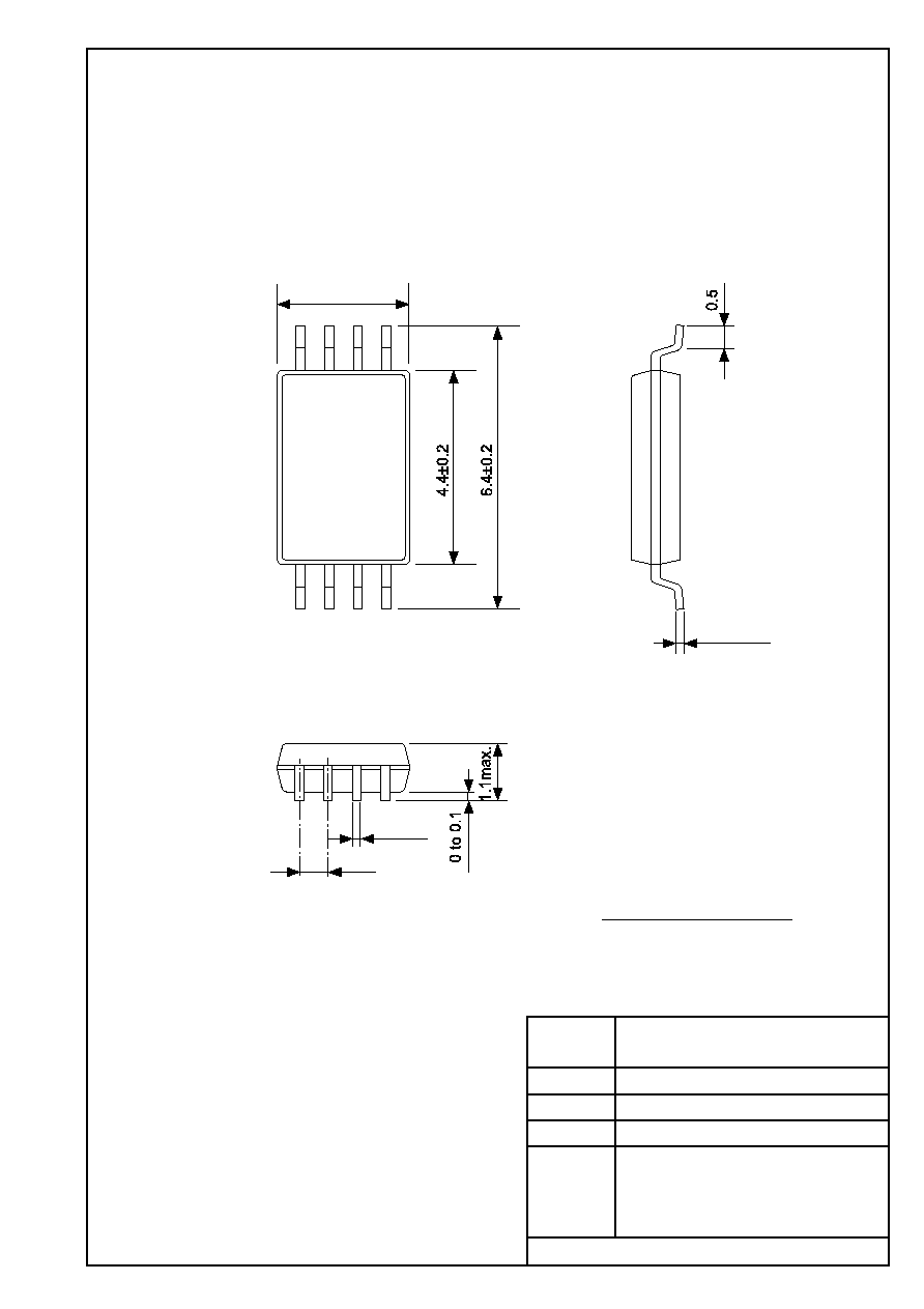
No.
TITLE
SCALE
UNIT
mm
Seiko Instruments Inc.
0.17Ī0.05
3.00
+0.3
-0.2
0.65
0.2Ī0.1
1
4
5
8
TSSOP8-A-PKG Dimensions
No. FT008-A-P-SD-1.1
FT008-A-P-SD-1.1
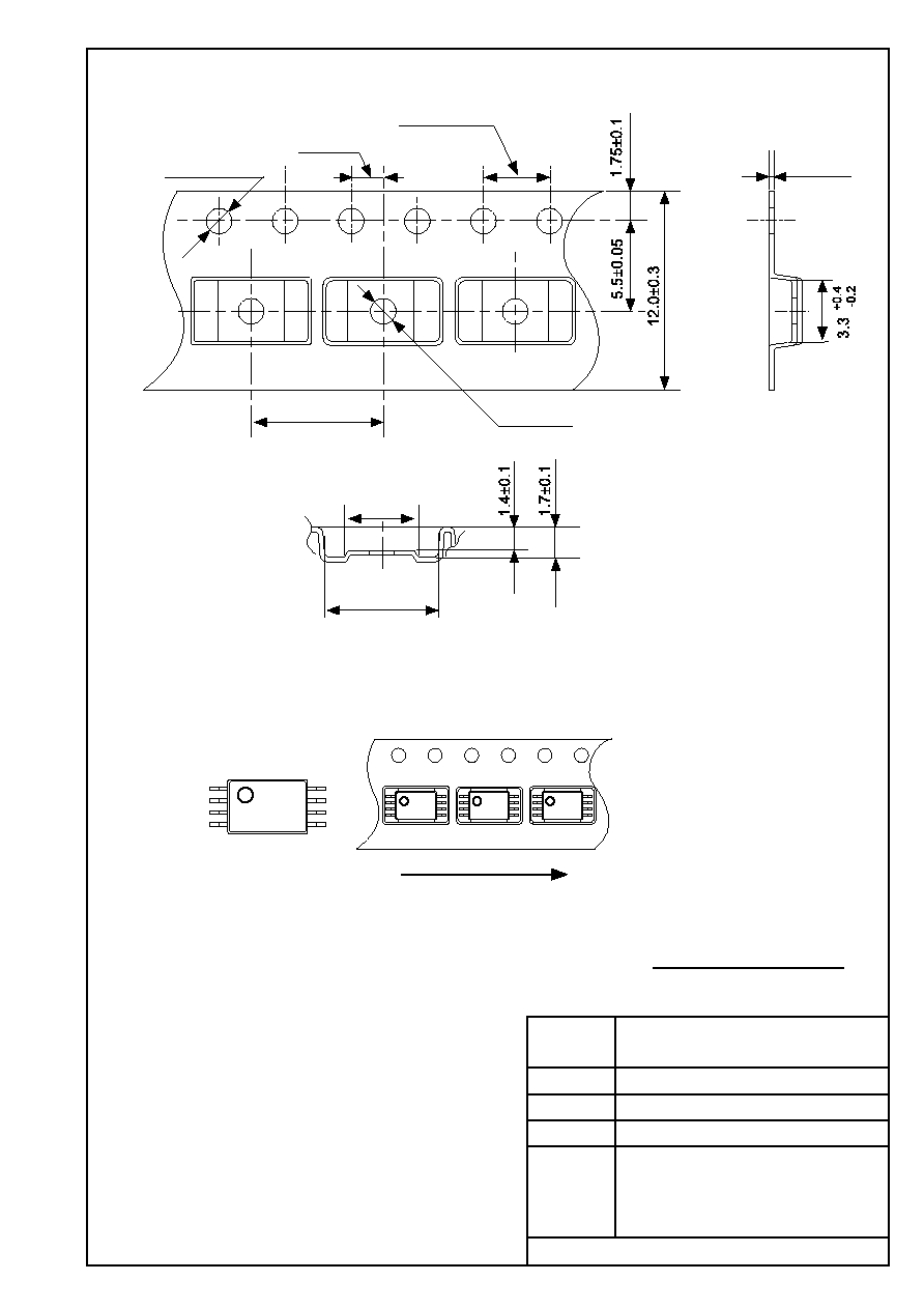
No.
TITLE
SCALE
UNIT
mm
Seiko Instruments Inc.
Ý1.55Ī0.05
2.0Ī0.05
8.0Ī0.1
Ý1.55
+0.1
-0.05
(4.4)
0.3Ī0.05
1
4
5
8
4.0Ī0.1
Feed direction
TSSOP8-E-Carrier Tape
No. FT008-E-C-SD-1.0
FT008-E-C-SD-1.0
+0.4
-0.2
6.6

No.
TITLE
SCALE
UNIT
mm
Seiko Instruments Inc.
Enlarged drawing in the central part
No. FT008-E-R-SD-1.0
2Ī0.5
Ý13Ī0.5
Ý21Ī0.8
13.4Ī1.0
17.5Ī1.0
3,000
QTY.
TSSOP8-E-Reel
FT008-E-R-SD-1.0

∑
The information described herein is subject to change without notice.
∑
Seiko Instruments Inc. is not responsible for any problems caused by circuits or diagrams described herein
whose related industrial properties, patents, or other rights belong to third parties. The application circuit
examples explain typical applications of the products, and do not guarantee the success of any specific
mass-production design.
∑
When the products described herein are regulated products subject to the Wassenaar Arrangement or other
agreements, they may not be exported without authorization from the appropriate governmental authority.
∑
Use of the information described herein for other purposes and/or reproduction or copying without the
express permission of Seiko Instruments Inc. is strictly prohibited.
∑
The products described herein cannot be used as part of any device or equipment affecting the human
body, such as exercise equipment, medical equipment, security systems, gas equipment, or any apparatus
installed in airplanes and other vehicles, without prior written permission of Seiko Instruments Inc.
∑
Although Seiko Instruments Inc. exerts the greatest possible effort to ensure high quality and reliability, the
failure or malfunction of semiconductor products may occur. The user of these products should therefore
give thorough consideration to safety design, including redundancy, fire-prevention measures, and
malfunction prevention, to prevent any accidents, fires, or community damage that may ensue.