
Rev.2.1
_60
Seiko Instruments Inc.
1
PWM Control & PWM/PFM Control
High-Frequency Step-Up Switching Regulator-Controllers
S-8340/8341 Series
The S-8340/8341 Series consists of CMOS step-up switching regulator-
controllers with PWM control (S-8340) and PWM/PFM switched control (S-
8341). These devices contain a reference voltage source, oscillation circuit,
error amplifier, phase compensation circuit, PWM control circuit, and other
components. Since the oscillation frequency is a high 300 kHz or 600 kHz,
with the addition of a small external component, the ICs can function as
step-up switching regulators with high efficiency and large output current.
The speed of the output stage is enhanced so that the Nch power MOS with
a low ON resistance can be switched quickly.
The S-8340 provides low-ripple power, high-efficiency, and excellent
transient characteristics thanks to a PMW control circuit capable of varying
the duty ratio linearly from 0
% to 82 % and optimized error amplifier, and
phase compensation circuit.
The S-8341 contains a PWM/PFM switching control circuit so that it
operates using PWM control with a duty ratio of 27
% or higher and using
PFM control with a duty ratio of lower than 27
% to ensure high efficiency in
all load ranges. These ICs serve as ideal main power supply units for
portable devices when coupled with the 8-Pin TSSOP package and high
oscillation frequencies.
Features
∑ Oscillation frequency:
600 kHz (A & B Series), 300 kHz (C & D Series).
∑ Output voltage:
Internally selectable in the range 2.5 V to 6.0 V in steps of 0.1 V (Output voltage fixed output
type)
∑ Output voltage precision: ±2.0 %
∑ Output voltage external setting (FB) type available. FB terminal voltage (V
FB
) 1.0 V
∑ The only peripheral components that can be used with this IC are a transistor, a coil, a diode,
capacitors (3), and a resistor.
∑ Duty ratio: 0 % to 82 % typ. PWM control (S-8340)
27
% to 82 % typ. PWM/PFM-switched control (S-8341, A & B Series)
21
% to 82 % typ. PWM/PFM-switched control (S-8341, C & D Series)
∑ Low-voltage operation: Oscillation can start when V
DD
=0.9 V.
∑ Built-in current limiting circuit: Can be set with an external resistor (R
SENSE
).
∑ Soft-start function: Can be set with an external capacitor (C
SS
).
∑ With a power-off function.
Package
∑ 8-Pin TSSOP (PKG drawing code: FT008-A)
Applications
∑ Power supplies for PDAs, electronic notebooks, and portable devices.
∑ Power supplies for audio equipment, including portable CD players, portable MD players and
headphone stereo equipment.
∑ Main and sub power supplies for notebook computers and peripheral equipment.
∑ Fixed voltage power supply for cameras, video equipment and communications equipment.

PWM Control & PWM/PFM Control High-Frequency Step-Up Switching Regulator-Controllers
S-8340/8341 Series
Rev.2.1
_60
Seiko Instruments Inc.
2
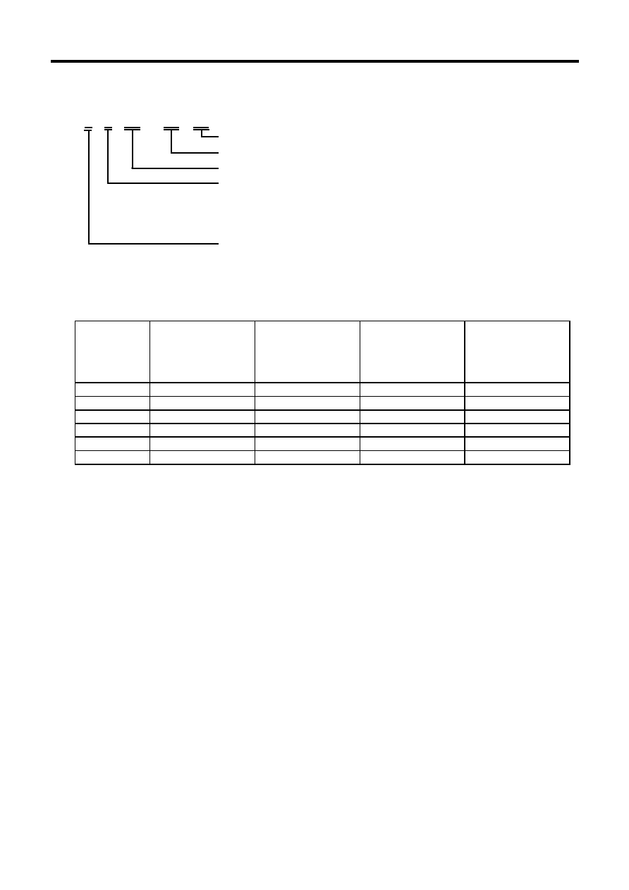
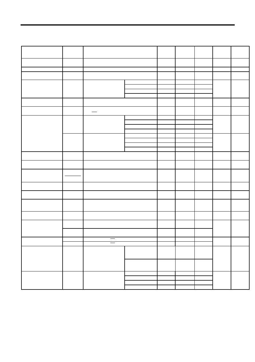
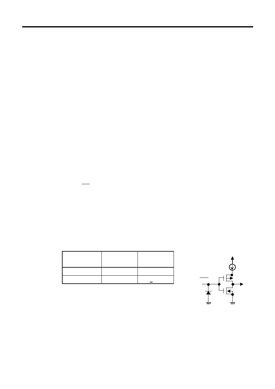
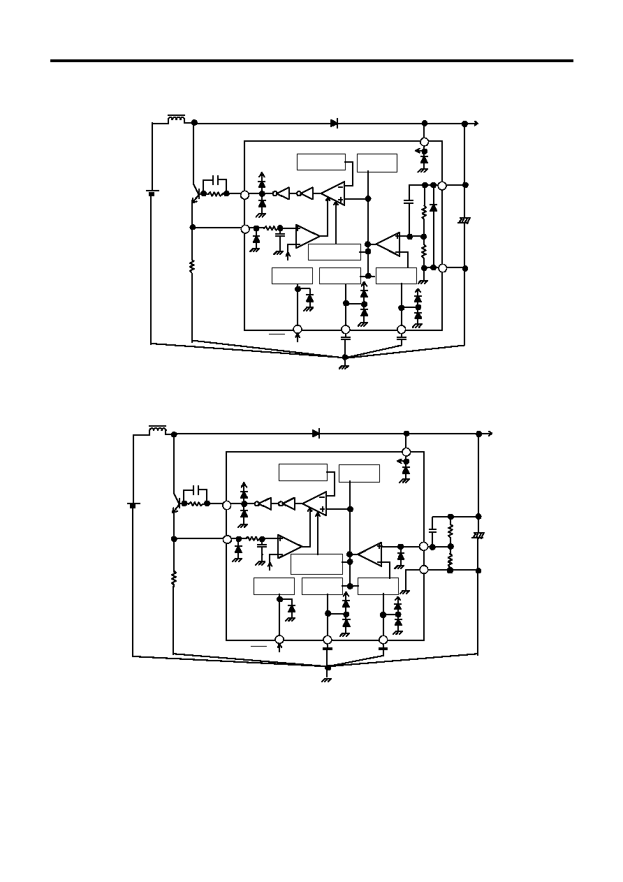
Block Diagram
C
S
R
S
R2
R1
C
C
VSS
V
OUT
VOUT
SD
C
L
ON /OFF
PWM, PWM/PFM
switching control
circuit
Phase
compensation
circuit
Triangular wave
oscillation circuit
VDD
L
EXT
Voltage/current
reference
Power-off
circuit
V
IN
C
VREF
C
SS
Nch Power
MOS FET
Soft-start
circuit
IC internal power
supply
120 mV
R
SENSE
SENSE
PWM comparator
Error amplifier
VREF
=
=
=
=1.0 V
+
CSS
CVREF
Figure 1 Block diagram <Output voltage fixed output type>
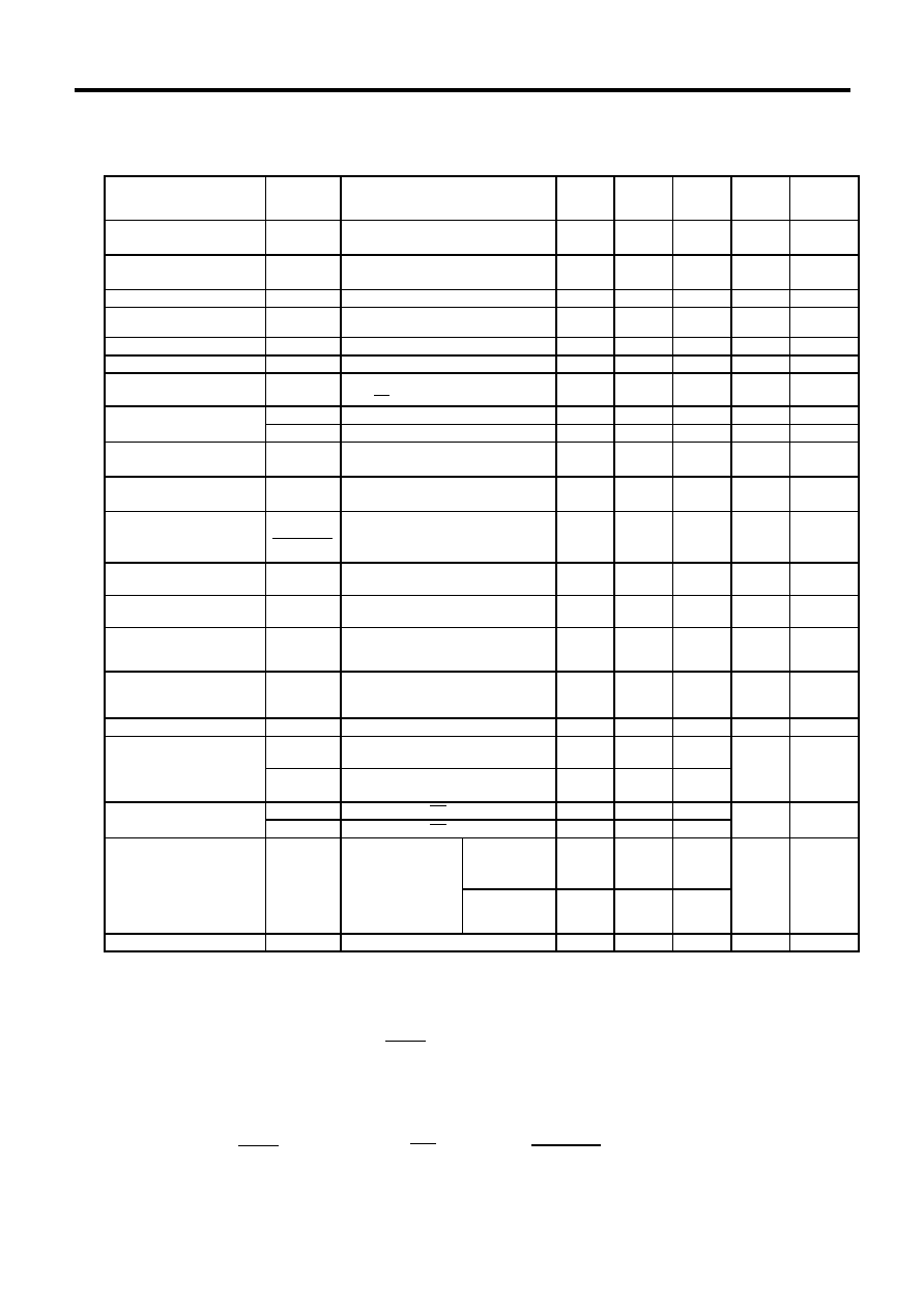
SD
ON /OFF
PWM, PWM/PFM
switching control
circuit
Phase
compensation
circuit
Triangular wave
oscillation circuit
VDD
L
EXT
Voltage/current
reference
Power-off
circuit
V
IN
C
VREF
C
SS
Nch Power
MOS FET
Soft-start
circuit
IC internal power
supply
120 mV
R
SENSE
SENSE
PWM comparator
Error amplifier
VREF
=
=
=
=1.0 V
+
V
OUT
C
S
R
S
FB
VSS
C
FB
C
L
R
FB1
R
FB2
CSS
CVREF
Figure 2 Block diagram <Output voltage external setting type>
PWM Control & PWM/PFM Control High-Frequency Step-Up Switching Regulator-Controllers
Rev.2.1
_
60
S-8340/8341 Series
Seiko Instruments Inc.
3
Selection Guide
1. Product Name
S-834X X
XX A FT - T2
Taping specifications
Package type
Output voltage
◊ 10
A;Output voltage fixed output type, fosc=600 kHz
B;Output voltage external setting type, fosc=600 kHz
C;Output voltage fixed output type, fosc=300 kHz
0;
D;Output voltage external setting type, fosc=300 kHz
PWM control
1; PWM/PFM-switched control
2. Product List
2-1. Output voltage fixed output type
Item
Output Voltage
(V)
S-8340AXXAFT
Series
fosc
= 600 kHz
PWM control
S-8341AXXAFT
Series
fosc
= 600 kHz
PWM/PFM-switched
control
S-8340CXXAFT
Series
fosc
= 300 kHz
PWM control
S-8341CXXAFT
Series
fosc
= 300 kHz
PWM/PFM-switched
control
2.5 V
± 2.0 %
S-8340A25AFT-T2
S-8341A25 AFT-T2
S-8340C25AFT-T2
S-8341C25 AFT-T2
3.0 V
± 2.0 %
S-8340A30AFT-T2
S-8341A30 AFT-T2
S-8340C30AFT-T2
S-8341C30 AFT-T2
3.3 V
± 2.0 %
S-8340A33AFT-T2
S-8341A33 AFT-T2
S-8340C33AFT-T2
S-8341C33 AFT-T2
5.0 V
± 2.0 %
S-8340A50AFT-T2
S-8341A50 AFT-T2
S-8340C50AFT-T2
S-8341C50 AFT-T2
5.6 V
± 2.0 %
S-8340A56AFT-T2
6.0 V
± 2.0 %
S-8340A60AFT-T2
S-8340C60AFT-T2
For the availability of other output voltage product, contact the SII Sales Department.
2.2. Output voltage external setting type
S-8340B00AFT-T2
:
fosc
= 600 kHz, PWM control
S-8341B00AFT-T2
:
fosc
= 600 kHz, PWM/PFM-switched control
S-8340D00AFT-T2
:
fosc
= 300 kHz, PWM control
S-8341D00AFT-T2
:
fosc
= 300 kHz, PWM/PFM-switched control
PWM Control & PWM/PFM Control High-Frequency Step-Up Switching Regulator-Controllers
S-8340/8341 Series
Rev.2.1
_60
Seiko Instruments Inc.
4
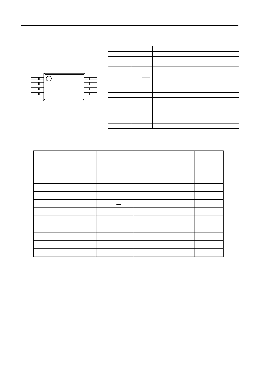
Pin Assignment
See the detailed drawing of the package at the end of this document.
2
1
3
4
8-Pin TSSOP
Top view
6
7
8
5
Figure 3
Absolute Maximum Ratings
(Ta
= 25∞C unless otherwise specified)
Item
Symbol
Ratings
Units
VDD pin voltage
V
DD
V
SS
-0.3 to V
SS
+12
V
VOUT pin voltage
V
OUT
V
SS
-0.3 to V
SS
+12
V
FB pin voltage
V
FB
V
SS
-0.3 to V
SS
+12
V
CVREF pin voltage
V
CVREF
V
SS
-0.3 to V
DD
+0.3
V
CSS pin voltage
V
CSS
V
SS
-0.3 to V
DD
+0.3
V
ON/OFF pin voltage
V
ON/OFF
V
SS
-0.3 to V
SS
+12
V
SENSE pin voltage
V
SENSE
V
SS
-0.3 to V
SS
+12
V
EXT pin voltage
V
EXT
V
SS
-0.3 to V
DD
+0.3
V
EXT pin current
I
EXT
±100
mA
Power dissipation
P
D
300
mW
Operating temperature range
T
OPR
-40 to 85
∞C
Storage temperature range
T
STG
-40 to 125
∞C
Caution The absolute maximum ratings are rated values exceeding which the product could
suffer physical damage. These values must therefore not be exceeded under any
conditions.
Pin No.
Pin Name
Function
1
VSS
GND pin
2
CVREF Reference voltage source pass capacitor
connection pin
3
CSS
Soft-start capacitor connection pin
4
ON/OFF
Power-off pin
H: Normal operation (Step-up operation)
L: Step-up operation stopped (All circuits
deactivated)
5
VDD
IC power supply pin
6
VOUT
(FB)
Output voltage fixed output type;
Output voltage monitoring pin
[Output voltage external setting type;
Feedback pin]
7
EXT
Connection pin for external transistor
8
SENSE Current limit detection pin
PWM Control & PWM/PFM Control High-Frequency Step-Up Switching Regulator-Controllers
Rev.2.1
_
60
S-8340/8341 Series
Seiko Instruments Inc.
5
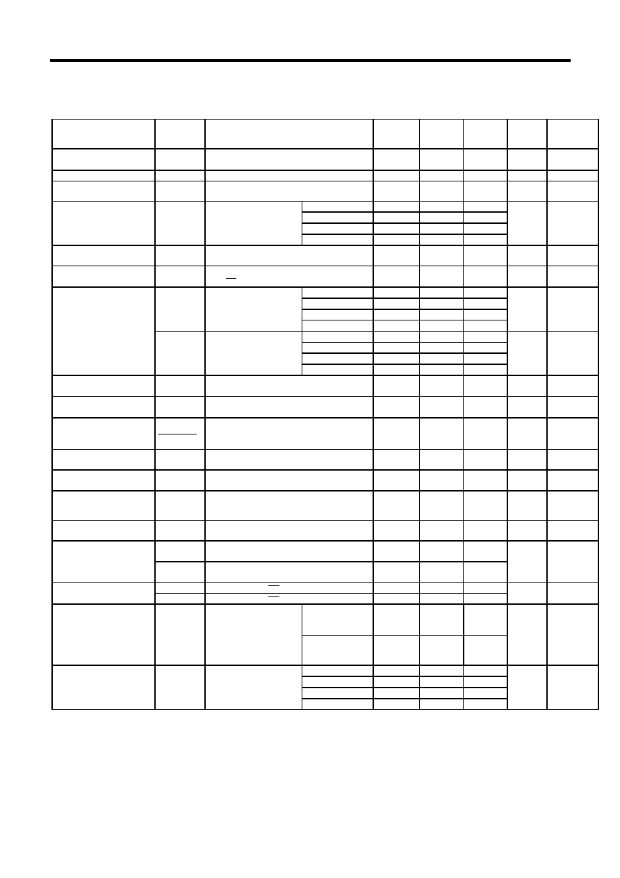
Electrical Characteristics
1. S-834xAxxAFT
(Ta
= 25 ∞C, unless otherwise specified)
Parameter
Symbol
Conditions
Min.
Typ.
Max.
Units
Measure-
ment
Circuit
Output voltage
*1
V
OUT
(E)
V
IN
= V
OUT
(S)
◊ 0.6
I
OUT
= V
OUT
(S) / 50
V
OUT
(S)
◊ 0.98
V
OUT
(S)
V
OUT
(S)
◊ 1.02
V
1
Input voltage
V
IN
-
-
-
6
V
1
Oscillation start voltage
V
ST
No external component.
The voltage is applied to VOUT.
-
-
0.9
V
2
S-834xA25
- 34
-
350
640
Current consumption 1
I
SS1
V
OUT
= V
OUT
(S)
◊ 0.95
S-834xA35
- 44
-
460
810
µA
2
EXT pin open
S-834xA45
- 54
-
630
1060
S-834xA55
- 60
-
810
1250
Current consumption 2
I
SS2
V
OUT
= V
OUT
(S)
+ 0.5 V
EXT pin open
-
180
300
µA
2
Current consumption
during power off
I
SSS
V
OUT
= V
OUT
(S)
◊ 0.95
V
ON/OFF
= 0 V
-
-
3.0
µA
2
S-834xA25
- 34
-13
-24
-
I
EXTH
V
EXT
= V
OUT
(E)
- 0.2 V
S-834xA35
- 44
-17
-30
-
mA
-
S-834xA45
- 54
-21
-34
-
EXT pin output current
S-834xA55
- 60
-23
-37
-
S-834xA25
- 34
32
56
-
I
EXTL
V
EXT
= 0.2 V
S-834xA35
- 44
42
69
-
mA
-
S-834xA45
- 54
50
78
-
S-834xA55
- 60
56
85
-
Line regulation
V
OUT1
V
OUT
(S)
◊ 0.4 V
IN
V
OUT
(S)
◊ 0.6
I
OUT
= V
OUT
(S) / 50
-
V
OUT
(S)
◊ 0.5 %
V
OUT
(S)
◊ 1 %
V
1
Load regulation
V
OUT2
V
IN
= V
OUT
(S)
◊ 0.6
10
µA I
OUT
V
OUT
(S) / 40
-
V
OUT
(S)
◊ 0.5 %
V
OUT
(S)
◊ 1 %
V
1
Output voltage
temperature coefficient
*2
V
OUT
Ta V
OUT
V
IN
= V
OUT
(S)
◊ 0.6
I
OUT
= V
OUT
(S) / 50
-40
∞C Ta 85 ∞C
-
±100
-
ppm/
∞C
1
Oscillation frequency
fosc
V
OUT
= V
OUT
(S)
◊ 0.95
Measure waveform at EXT pin
510
600
690
kHz
2
Maximum duty ratio
MaxDuty
V
IN
= V
OUT
(S)
◊ 0.95
Measure waveform at EXT pin
73
82
89
%
2
PWM/PFM-control
switch duty ratio
(S-8341AxxAFT)
PFM Duty
V
IN
= V
OUT
(E)
- 0.1 V
Under no load
19
27
35
%
1
Current limit detection
voltage
V
SENSE
V
OUT
= V
OUT
(S)
◊ 0.95
Judge oscillation stop in "L", at EXT pin.
90
120
150
mV
2
Power-Off pin
V
SH
V
OUT
= V
OUT
(S)
◊ 0.95
Judge oscillation at EXT pin.
0.8
-
-
V
2
input voltage
V
SL
V
OUT
= V
OUT
(S)
◊ 0.95
Judge oscillation stop at EXT pin.
-
-
0.3
Power-Off pin
I
SH
V
OUT
= 6 V, V
ON/OFF
= 6 V
-0.1
-
0.1
µA
2
input leakage current
I
SL
V
OUT
= 6 V, V
ON/OFF
= 0 V
-0.1
-
0.1
Soft-Start time
T
SS
V
IN
= V
OUT
(S)
◊ 0.6,
C
SS
= 4700 pF
I
OUT
= V
OUT
(S) / 50
S-8340Axx
3.0
6.0
14.0
ms
1
Measure time until
oscillation occurs at
EXT pin.
S-8341Axx
3.0
8.0
14.0
S-834xA25
- 34
-
83
-
Efficiency
EFFI
V
IN
= V
OUT
(S)
◊ 0.6
S-834xA35
- 44
-
85
-
%
1
I
OUT
=V
OUT
(S) / 50
S-834xA45
- 54
-
87
-
S-834xA55
- 60
-
87
-
*1.
V
OUT
(S): Set output voltage value
V
OUT
(E): Actual output voltage value: Output voltage value when I
OUT
=V
OUT
(S)/50
and V
IN
=V
OUT
(S)
◊0.6.

PWM Control & PWM/PFM Control High-Frequency Step-Up Switching Regulator-Controllers
S-8340/8341 Series
Rev.2.1
_60
Seiko Instruments Inc.
6
*2.
The change of output voltage with temperature [mV/
∞C] is calculated from the following formula:
Conditions:
Peripheral components:
Coil
: Sumida Electric Co., Ltd. CD54 (10
µH).
Diode
: Matsushita Electronics Corporation MA735 (Schottky type).
Capacitor
: Nichicon Corporation. F93 (16 V, 47
µF tantalum type).
Transistor
: Sanyo Electric Co., Ltd 2SD 1628G.
Base resistor (R
b
)
: 1.0 k
Base capacitor (C
b
)
: 2200 pF (Ceramic type)
C
VREF
: 0.01
µF
C
SS
: 4700 pF
VDD pin is connected to VOUT pin.
The power-off pin is connected to VOUT pin, SENSE pin is connected to VSS pin, unless otherwise specified.
Note 1:
Boost operation is performed from V
DD
=0.9 V. However, 2.5 V or more for VDD is recommended to stabilize the output
voltage and oscillation frequency. If V
DD
is taken from V
IN
or other power sources, instead of V
OUT
, V
DD
should be 2.5 V
or more. However, if V
DD
is not taken from V
OUT
, the output voltage precision of
±2.0 % is not guaranteed due to
dependency of output voltage on V
DD
. In particular, accuracy of output voltage is degraded significantly when the V
DD
voltage is 6.0 V or more. Therefore, do not use this IC when V
DD
voltage is 6.0 V or more. If V
DD
of 2.5 V or more is
applied, increase power supply so that V
DD
becomes 2.5 V or more within the soft-start time (3 ms).
V
OUT
TaV
OUT
(Output voltage temperature factor)
(Change of output voltage with
temperature)
(Set output voltage
value)
[mV/
∞C]
V
OUT
Ta
V
OUT
(S)[V]
=
◊
[ppm/
∞C] ˜ 1000
PWM Control & PWM/PFM Control High-Frequency Step-Up Switching Regulator-Controllers
Rev.2.1
_
60
S-8340/8341 Series
Seiko Instruments Inc.
7
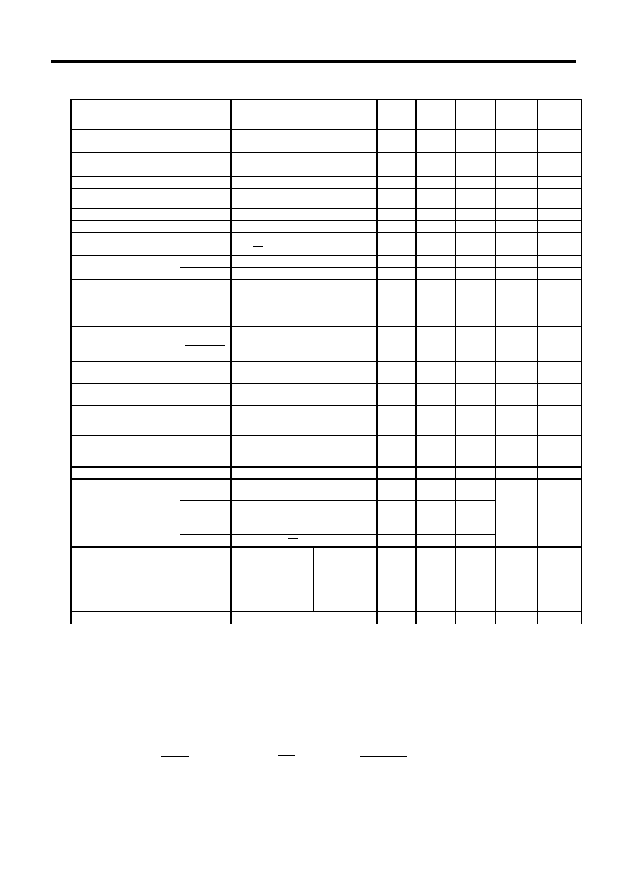
2. S-834xB00AFT
(Ta
= 25 ∞C, unless otherwise specified)
Parameter
Symbol
Conditions
Min.
Typ.
Max.
Units
Measure
-ment
Circuit
Output voltage
*1
V
OUT
(E)
V
IN
=2.4 V
I
OUT
=80 mA
3.920
4.000
4.080
V
3
FB pin voltage
V
FB
V
IN
=2.4 V
I
OUT
=80 mA
0.980
1.000
1.020
V
3
Input voltage
V
IN
-
-
-
6
V
3
Oscillation start voltage
V
ST2
No external component.
The voltage is applied to VDD.
-
-
0.9
V
4
Current consumption 1
I
SS1
V
OUT
=3.8 V
-
460
740
µA
4
Current consumption 2
I
SS2
V
OUT
=4.5 V
-
180
300
µA
4
Current consumption
during power off
I
SSS
V
OUT
=3.8 V
V
ON/OFF
= 0 V
-
-
3.0
µA
4
EXT pin output current
I
EXTH
V
EXT
= V
OUT
(E)
- 0.2 V
-19
-30
-
mA
-
I
EXTL
V
EXT
=0.2 V
46
69
-
mA
-
Line regulation
V
OUT1
1.6 V
V
IN
2.4 V
I
OUT
=80 mA
-
20
40
mV
3
Load regulation
V
OUT2
V
IN
=2.4 V
10
µA I
OUT
100 mA
-
20
40
mV
3
Output voltage
temperature coefficient
*2
V
OUT
TaV
OUT
V
IN
=2.4 V
I
OUT
=80 mA
-40∞C Ta 85∞C
-
±100
-
ppm/∞C
3
Oscillation frequency
fosc
V
OUT
=3.8 V
Measure waveform at EXT pin
510
600
690
kHz
4
Maximum duty ratio
MaxDuty
V
IN
=3.8 V
Measure waveform at EXT pin
73
82
89
%
4
PWM/PFM-control
switch duty ratio
(S-8341B00AFT)
PFMDuty
V
IN
=V
OUT
(E)
-0.1 V
Under no load
19
27
35
%
3
Current limit detection
voltage
V
SENSE
V
OUT
=3.8 V
Judge oscillation stop in "L", at EXT
pin.
90
120
150
mV
4
FB pin input current
I
FB
V
OUT
=6 V, V
FB
=1.5 V
-50
-
50
nA
4
Power-Off pin
V
SH
V
OUT
=3.8 V
Judge oscillation at EXT pin.
0.8
-
-
V
4
input voltage
V
SL
V
OUT
=3.8 V
Judge oscillation stop at EXT pin.
-
-
0.3
Power-Off pin
I
SH
V
OUT
=6 V,V
ON/OFF
=6 V
-0.1
-
0.1
µA
4
input leakage current
I
SL
V
OUT
=6 V,V
ON/OFF
=0 V
-0.1
-
0.1
Soft-Start time
T
SS
V
IN
=2.4 V,
C
SS
=4700 pF
I
OUT
=80 mA
S-8340B00
3.0
6.0
14.0
ms
3
Measure time until
oscillation occurs
at EXT pin.
S-8341B00
3.0
8.0
14.0
Efficiency
EFFI
V
IN
=2.4 V, I
OUT
=80 mA
-
85
-
%
3
*1.
V
OUT
(E): Actual output voltage value: Output voltage value when I
OUT
=80 mA and V
IN
=2.4 V is input.
300k
100k
*2.
Change of output voltage with temperature
[ mV / ∞C ] is represented by the following equation:
However, the temperature change rates for R
FB1
and R
FB2
are assumed to be the same.
= (
1+
R
R
FB1
FB2
)
V
OUT
TaV
OUT
(
Output voltage temperature factor
)
(
Change of output voltage with temperature
) (
Set output voltage value
)
[mV/
∞C]
V
OUT
Ta
◊
[ppm/
∞C] ˜ 1000
Typ. value (set output voltage value) is 1+
[V].

PWM Control & PWM/PFM Control High-Frequency Step-Up Switching Regulator-Controllers
S-8340/8341 Series
Rev.2.1
_60
Seiko Instruments Inc.
8
Conditions:
Peripheral components:
Coil
: Sumida Electric Co., Ltd. CD54 (10
µH).
Diode
: Matsushita Electronics Corporation MA735 (Schottky type).
Capacitor
: Nichicon Corporation F93 (16 V, 47
µF tantalum type).
Transistor
: Sanyo Electric Co., Ltd. 2SD 1628G.
Base resistor (R
b
)
: 1.0 k
Base capacitor (C
b
)
: 2200 pF (Ceramic type)
C
VREF
: 0.01
µF
C
SS
: 4700 pF
R
FB1
: 300 k
R
FB2
: 100 k
C
FB
: 50 pF
The power-off pin is connected to VOUT pin, SENSE pin is connected to VSS pin, unless otherwise specified.
Note 1:
Boost operation is performed from V
DD
=0.9 V. However, 2.5 V or more for VDD is recommended to stabilize the output
voltage and oscillation frequency. If V
DD
is taken from V
IN
or other power sources, instead of V
OUT
, V
DD
should be 2.5 V
or more. The output voltage precision is applicable when V
DD
is 4.0 V. It should be noted that if V
DD
is not 4.0 V, the
output voltage precision of
±2.0 % cannot be guaranteed due to dependency of output voltage on V
DD
. In particular,
accuracy of output voltage is degraded significantly when the V
DD
voltage is 6.0 V or more. Therefore, do not use this
IC when V
DD
voltage is 6.0 V or more. If V
DD
of 2.5 V or more is applied, increase power supply so that V
DD
becomes
2.5 V or more within the soft-start time (3 ms).
PWM Control & PWM/PFM Control High-Frequency Step-Up Switching Regulator-Controllers
Rev.2.1
_
60
S-8340/8341 Series
Seiko Instruments Inc.
9
3. S-834xCxxAFT
(Ta
= 25 ∞C, unless otherwise specified)
Parameter
Symbol
Conditions
Min.
Typ.
Max.
Units
Measure
-ment
Circuit
Output voltage
*1
V
OUT
(E)
V
IN
= V
OUT
(S)
◊ 0.6
I
OUT
= V
OUT
(S) / 50
V
OUT
(S)
◊ 0.98
V
OUT
(S)
V
OUT
(S)
◊ 1.02
V
1
Input voltage
V
IN
-
-
-
6
V
1
Oscillation start voltage
V
ST
No external component.
The voltage is applied to VOUT.
-
-
0.9
V
2
S-834xC25
- 34
-
210
430
Current consumption 1
I
SS1
V
OUT
= V
OUT
(S)
◊ 0.95
S-834xC35
- 44
-
270
520
µA
2
EXT pin open
S-834xC45
- 54
-
350
650
S-834xC55
- 60
-
440
740
Current consumption 2
I
SS2
V
OUT
= V
OUT
(S)
+ 0.5 V
EXT pin open
-
110
185
µA
2
Current consumption
during power off
I
SSS
V
OUT
= V
OUT
(S)
◊ 0.95
V
ON/OFF
= 0 V
-
-
3.0
µA
2
S-834xC25
- 34
-13
-24
-
I
EXTH
V
EXT
= V
OUT
(E)
- 0.2 V
S-834xC35
- 44
-17
-30
-
mA
-
S-834xC45
- 54
-21
-34
-
EXT pin output current
S-834xC55
- 60
-23
-37
-
S-834xC25
- 34
32
56
-
I
EXTL
V
EXT
= 0.2 V
S-834xC35
- 44
42
69
-
mA
-
S-834xC45
- 54
50
78
-
S-834xC55
- 60
56
85
-
Line regulation
V
OUT1
V
OUT
(S)
◊ 0.4 V
IN
V
OUT
(S)
◊ 0.6
I
OUT
= V
OUT
(S) / 50
-
V
OUT
(S)
◊ 0.5 %
V
OUT
(S)
◊ 1 %
V
1
Load regulation
V
OUT2
V
IN
= V
OUT
(S)
◊ 0.6
10
µA I
OUT
V
OUT
(S) / 40
-
V
OUT
(S)
◊ 0.5 %
V
OUT
(S)
◊ 1 %
V
1
Output voltage
temperature coefficient
*2
V
OUT
Ta V
OUT
V
IN
= V
OUT
(S)
◊ 0.6
I
OUT
= V
OUT
(S) / 50
-40∞C Ta 85∞C
-
±100
-
ppm/
∞C
1
Oscillation frequency
fosc
V
OUT
= V
OUT
(S)
◊ 0.95
Measure waveform at EXT pin
255
300
345
kHz
2
Maximum duty ratio
MaxDuty
V
IN
= V
OUT
(S)
◊ 0.95
Measure waveform at EXT pin
73
82
89
%
2
PWM/PFM-control
switch duty ratio
(S-8341CxxAFT)
PFM Duty
V
IN
= V
OUT
(E)
- 0.1 V
Under no load
15
21
31
%
1
Current limit detection
voltage
V
SENSE
V
OUT
= V
OUT
(S)
◊ 0.95
Judge oscillation stop in "L", at EXT pin.
90
120
150
mV
2
Power-Off pin
V
SH
V
OUT
= V
OUT
(S)
◊ 0.95
Judge oscillation at EXT pin.
0.8
-
-
V
2
input voltage
V
SL
V
OUT
= V
OUT
(S)
◊ 0.95
Judge oscillation stop at EXT pin.
-
-
0.3
Power-Off pin
I
SH
V
OUT
= 6 V, V
ON/OFF
= 6 V
-0.1
-
0.1
µA
2
input leakage current
I
SL
V
OUT
= 6 V, V
ON/OFF
= 0 V
-0.1
-
0.1
Soft-Start time
T
SS
V
IN
= V
OUT
(S)
◊ 0.6, C
SS
= 4700 pF
I
OUT
= V
OUT
(S) / 50
S-8340Cxx
6.0
14.3
28.0
ms
1
Measure time until
oscillation occurs at
EXT pin.
S-8341Cxx
6.0
17.2
28.0
S-834xC25
- 34
-
83
-
Efficiency
EFFI
V
IN
= V
OUT
(S)
◊ 0.6
S-834xC35
- 44
-
85
-
%
1
I
OUT
=V
OUT
(S) / 50
S-834xC45
- 54
-
87
-
S-834xC55
- 60
-
87
-
*1.
V
OUT
(S): Set output voltage value
V
OUT
(E): Actual output voltage value: Output voltage value when I
OUT
=V
OUT
(S)/50
and V
IN
=V
OUT
(S)
◊0.6.

PWM Control & PWM/PFM Control High-Frequency Step-Up Switching Regulator-Controllers
S-8340/8341 Series
Rev.2.1
_60
Seiko Instruments Inc.
10
*2.
The change of output voltage with temperature [mV/
∞C] is calculated from the following formula:
Conditions:
Peripheral components:
Coil
: Sumida Electric Co., Ltd. CD54 (10
µH).
Diode
: Matsushita Electronics Corporation MA735 (Schottky type).
Capacitor
: Nichicon Corporation F93 (16 V, 47
µF tantalum type).
Transistor
: Sanyo Electric Co., Ltd. 2SD 1628G.
Base resistor (R
b
)
: 1.0 k
Base capacitor (C
b
)
: 2200 pF (Ceramic type)
C
VREF
: 0.01
µF
C
SS
: 4700 pF
VDD pin is connected to VOUT pin.
The power-off pin is connected to VOUT pin, SENSE pin is connected to VSS pin, unless otherwise specified.
Note 1:
Boost operation is performed from V
DD
=0.9 V. However, 2.5 V or more for VDD is recommended to stabilize the output
voltage and oscillation frequency. If V
DD
is taken from V
IN
or other power sources, instead of V
OUT
, V
DD
should be 2.5 V
or more. However, if V
DD
is not taken from V
OUT
, the output voltage precision of ±2.0
% is not guaranteed due to
dependency of output voltage on V
DD
. In particular, accuracy of output voltage is degraded significantly when the V
DD
voltage is 6.0 V or more. Therefore, do not use this IC when V
DD
voltage is 6.0 V or more. If V
DD
of 2.5 V or more is
applied, increase power supply so that V
DD
becomes 2.5 V or more within the soft-start time (6 ms).
V
OUT
TaV
OUT
(Output voltage temperature factor)
(Change of output voltage with temperature) (Set output voltage
value)
[mV/
∞C]
V
OUT
Ta
V
OUT
(S)[V]
=
◊
[ppm/
∞C] ˜ 1000
PWM Control & PWM/PFM Control High-Frequency Step-Up Switching Regulator-Controllers
Rev.2.1
_
60
S-8340/8341 Series
Seiko Instruments Inc.
11
Typ. value (set output voltage value) is 1+
[V].
4. S-834xD00AFT
(Ta
= 25 ∞C, unless otherwise specified)
Parameter
Symbol
Conditions
Min.
Typ.
Max.
Units
Measure-
ment
Circuit
Output voltage
*1
V
OUT
(E)
V
IN
=2.4 V
I
OUT
=80 mA
3.920
4.000
4.080
V
3
FB pin voltage
V
FB
V
IN
=2.4 V
I
OUT
=80 mA
0.980
1.000
1.020
V
3
Input voltage
V
IN
-
-
-
6
V
3
Oscillation start voltage
V
ST2
No external component.
The voltage is applied to VDD.
-
-
0.9
V
4
Current consumption 1
I
SS1
V
OUT
=3.8 V
-
255
460
µA
4
Current consumption 2
I
SS2
V
OUT
=4.5 V
-
110
185
µA
4
Current consumption
during power off
I
SSS
V
OUT
=3.8 V
V
ON/OFF
= 0 V
-
-
3.0
µA
4
EXT pin output current
I
EXTH
V
EXT
= V
OUT
(E)
- 0.2 V
-19
-30
-
mA
-
I
EXTL
V
EXT
=0.2 V
46
69
-
mA
-
Line regulation
V
OUT1
1.6 V
V
IN
2.4 V
I
OUT
=80 mA
-
20
40
mV
3
Load regulation
V
OUT2
V
IN
=2.4 V
10
µA I
OUT
100 mA
-
20
40
mV
3
Output voltage
temperature coefficient
*2
V
OUT
TaV
OUT
V
IN
=2.4 V
I
OUT
=80 mA
-40 ∞C Ta 85 ∞C
-
±100
-
ppm/∞C
3
Oscillation frequency
fosc
V
OUT
=3.8 V
Measure waveform at EXT pin
255
300
345
kHz
4
Maximum duty ratio
MaxDuty
V
IN
=3.8 V
Measure waveform at EXT pin
73
82
89
%
4
PWM/PFM-control
switch duty ratio
(S-8341D00AFT)
PFMDuty
V
IN
= V
OUT
(E)
-0.1 V
Under no load
15
21
31
%
3
Current limit detection
voltage
V
SENSE
V
OUT
=3.8 V
Judge oscillation stop in "L", at EXT
pin.
90
120
150
mV
4
FB pin input current
I
FB
V
OUT
=6 V, V
FB
=1.5 V
-50
-
50
nA
4
Power-Off pin
V
SH
V
OUT
=3.8 V
Judge oscillation at EXT pin.
0.8
-
-
V
4
input voltage
V
SL
V
OUT
=3.8 V
Judge oscillation stop at EXT pin.
-
-
0.3
Power-Off pin
I
SH
V
OUT
=6 V,V
ON/OFF
=6 V
-0.1
-
0.1
µA
4
input leakage current
I
SL
V
OUT
=6 V,V
ON/OFF
=0 V
-0.1
-
0.1
Soft-Start time
T
SS
V
IN
=2.4 V,
C
SS
=4700 pF
I
OUT
=80 mA
S-8340D00
6.0
14.3
28.0
ms
3
Measure time until
oscillation occurs
at EXT pin.
S-8341D00
6.0
17.2
28.0
Efficiency
EFFI
V
IN
=2.4 V, I
OUT
=80 mA
-
85
-
%
3
*1.
V
OUT
(E): Actual output voltage value: Output voltage value when I
OUT
=80 mA and V
IN
=2.4 V is input.
300 k
100 k
*2.
Change of output voltage with temperature
[ mV / ∞C ] is represented by the following equation:
However, the temperature change rates for R
FB1
and R
FB2
are assumed to be the same.
= (
1+
R
R
FB1
FB2
)
V
OUT
TaV
OUT
(
Output voltage temperature factor
)
(
Change of output voltage with temperature
) (
Set output voltage value
)
[mV/
∞C]
V
OUT
Ta
◊
[ppm/
∞C] ˜ 1000
PWM Control & PWM/PFM Control High-Frequency Step-Up Switching Regulator-Controllers
S-8340/8341 Series
Rev.2.1
_60
Seiko Instruments Inc.
12
Conditions:
Peripheral components:
Coil
: Sumida Electric Co., Ltd. CD54 (10
µH).
Diode
: Matsushita Electronics Corporation MA735 (Schottky type).
Capacitor
: Nichicon Corporation F93 (16 V, 47
µF tantalum type).
Transistor
: Sanyo Electric Co., Ltd. 2SD 1628G.
Base resistor (R
b
)
: 1.0 k
Base capacitor (C
b
)
: 2200 pF (Ceramic type)
C
VREF
: 0.01
µF
C
SS
: 4700 pF
R
FB1
: 300 k
R
FB2
: 100 k
C
FB
: 50 pF
The power-off pin is connected to VOUT pin, SENSE pin is connected to VSS pin, unless otherwise specified.
Note 1:
Boost operation is performed from V
DD
=0.9 V. However, 2.5 V or more for VDD is recommended to stabilize the output
voltage and oscillation frequency. If V
DD
is taken from V
IN
or other power sources, instead of V
OUT
, V
DD
should be 2.5 V
or more. The output voltage precision is applicable when V
DD
is 4.0 V. It should be noted that if V
DD
is not 4.0 V, the
output voltage precision of
±2.0 % cannot be guaranteed due to dependency of output voltage on V
DD
. In particular,
accuracy of output voltage is degraded significantly when the V
DD
voltage is 6.0 V or more. Therefore, do not use this
IC when V
DD
voltage is 6.0 V or more. If V
DD
of 2.5 V or more is applied, increase power supply so that V
DD
becomes
2.5 V or more within the soft-start time (6 ms).
Measurement Circuits:
1.
+
+
-
-
L
R
L
C
L
C
IN
R
b
C
b
SD
V
IN
VDD
ON OFF
VSS
VOUT
EXT
CSS
CVREF
SENSE
V
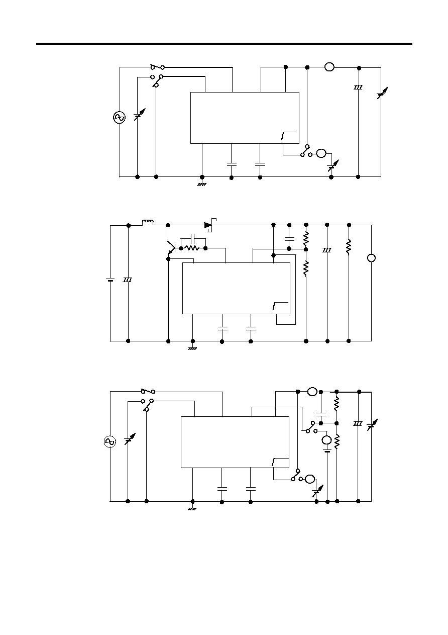
PWM Control & PWM/PFM Control High-Frequency Step-Up Switching Regulator-Controllers
Rev.2.1
_
60
S-8340/8341 Series
Seiko Instruments Inc.
13
2.
+
-
Oscilloscope
VDD
ON OFF
VSS
VOUT
EXT
CSS
CVREF
SENSE
A
A
3.
+
+
-
-
L
R
FB2
R
FB1
C
FB
R
L
C
L
C
IN
R
b
C
b
SD
V
IN
VDD
ON OFF
VSS
FB
EXT
CSS
CVREF
SENSE
V
4.
Oscilloscope
VDD
ON OFF
V
OUT
VSS
R
FB2
C
FB
R
FB1
FB
EXT
CSS
CVREF
SENSE
+
-
A
A
A
Figure 4
PWM Control & PWM/PFM Control High-Frequency Step-Up Switching Regulator-Controllers
S-8340/8341 Series
Rev.2.1
_60
Seiko Instruments Inc.
14
Operation
1. Switching control method
1.1 PWM Control (S-8340 Series)
The S-8340 Series consists of DC/DC converters that employ a pulse-width modulation (PWM) system.
In conventional PFM system DC/DC converters, pulses are skipped when they are operated with a low
output load current, causing variations in the ripple frequency of the output voltage and an increase in
the ripple voltage. Both of these effects constitute inherent drawbacks to those converters.
In converters of the S-8340 Series, the pulse width varies in a range from 0
% to 82 %, according to the
load current, and yet ripple voltage produced by the switching can easily be removed through a filter
because the switching frequency remains constant. Therefore, these converters provide a low-ripple
power over broad ranges of input voltage and load current.
1.2 PWM/PFM-Switched Control (S-8341 Series)
The S-8341 Series consists of DC/DC converters capable of automatically switching the pulse-wide
modulation system (PWM) over to the pulse-frequency modulation system (PFM), and vice versa,
according to the load current.
In a region of high output load currents, the S-8341 Series converters function with PWM control, where
the pulse-width duty varies from 27
% to 82 % (A&B Series) and from 21 % to 82 % (C&D Series). This
function realizes low ripple power.
For certain low output load currents, the converters are switched over to PFM control, whereby pulses
having their pulse-width duty fixed at 27
% (A&B Series) and 21 % (C&D Series) are skipped depending
on the quantity of the load current, and are output to a switching transistor. This causes the oscillation
circuit to produce intermittent oscillation. As a result, current consumption is reduced and efficiency
losses are prevented under low loads. Especially for output load currents in the region of 1 mA, these
DC/DC converters can operate at extremely high efficiency.
2. Power-Off Pin (ON/OFF Pin)
This pin deactivates or activates the step-up operation. When the power-off pin is set to "L", the VSS
voltage appears through the EXT pin, prodding the switching transistor to go off. All the internal circuits
stop working, and substantial savings in current consumption are thus achieved.
The power-off pin is configured as shown in Figure 5. Since pull-up or pull-down is not performed
internally, please avoid operating the pin in a floating state. Also, try to refrain from applying a voltage of
0.3 V to 0.8 V to the pin, less such voltage makes the power on/off state indefinite. When this power-off
pin is not used, leave it coupled to the VDD pin.
The power-off pin does not have hysterisis.
Power-Off Pin
CR Oscillation
Circuit
Output Voltage
"H"
Activated
Set value
"L"
Deactivated
V
IN
*
* Voltage obtained by extracting the voltage drop due to
DC resistance of the inductor and the diode forward
voltage from V
IN
.
ON/OFF
VDD
VSS
Figure 5
PWM Control & PWM/PFM Control High-Frequency Step-Up Switching Regulator-Controllers
Rev.2.1
_
60
S-8340/8341 Series
Seiko Instruments Inc.
15
3. Soft-Start Function
The S-8340/41 Series comes with a built-in soft-start circuit. This circuit enables the output voltage to
rise gradually over the specified soft-start time, when the power is switched on or when the power-off pin
is switched to "H" level. This prevents the output voltage from overshooting and suppresses a rush
current from the power supply.
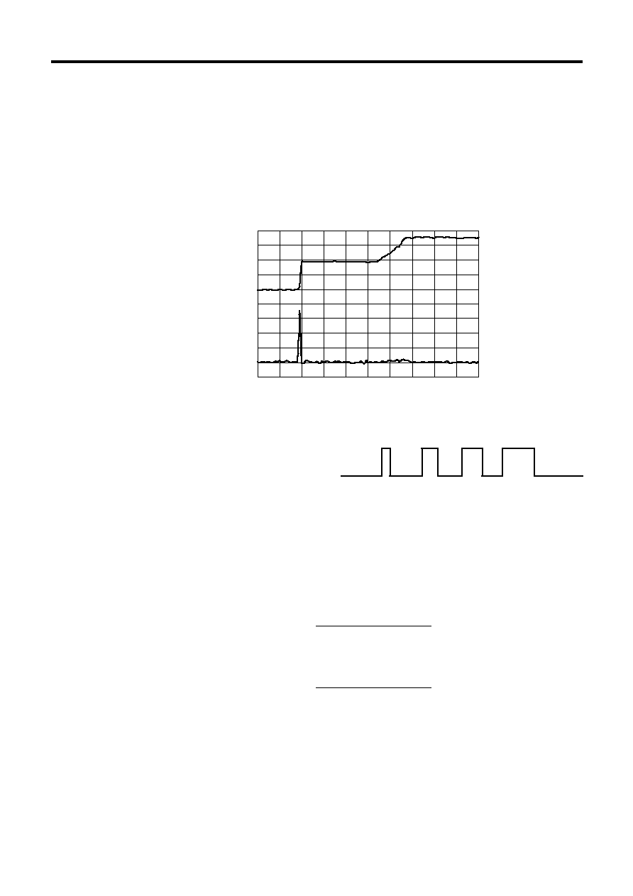
Generally, the step-up circuit flows a rush current to an output capacitor through an inductor and a diode
just when the power is turned on as shown in Fig. 6. The soft-start function of this IC, however, does not
limit this current.
t(2 ms/div)
Output voltage
(1 V/div)
Rush current
(0.5 A/div)
3 V
0 V
1.5 A
0 A
S-8340A33AFT (V
IN
=01.9 V,R
L
=300 k)
Figure 6 Waveforms of Output Voltage and Rush Current at Soft-Start
The soft-start circuit of the S-8340/41
increases the duty ratio gradually as shown
in Figure 7.
The soft-start time can be set with an
external capacitor (C
SS
).
If f
=600 kHz and C
SS
=4700 pF, the time until the duty ratio of 50 % is reached is 9.7 ms (typ.).
If V
IN
2 V, the time until a duty ratio is reached is calculated from the following formula:
If f
=600 kHz,
t[ms]
=C
SS
[pF]
◊
If f
=300 kHz,
t[ms]
=C
SS
[pF]
◊
Note:
Even if the IC reaches a certain duty at duty ratio of 0
% to 43 %, there may be a delay of the output
voltage V
OUT
in reaching the specified voltage V
OUT
(S). This delay occurs due to the delay of the error
amplifier reference voltage in reaching the specified voltage (1.0 V). If the worst comes to worst, delay
may occur until the time calculated when a duty ratio is 43
%.
Figure 7 Image of EXT pin waveform
8.336
◊ Duty[%]+682.4
535000
6.564
◊ Duty[%]+698
229000
PWM Control & PWM/PFM Control High-Frequency Step-Up Switching Regulator-Controllers
S-8340/8341 Series
Rev.2.1
_60
Seiko Instruments Inc.
16
4. Current Limit Circuit
The current limit circuit of the S-8340/41 series can limit current by inserting a sense resistor (R
SENSE
)
between an external FET source or an external NPN bipolar transistor emitter and Vss and entering a
connection point with a sensor resistor into the SENSE pin to prevent thermal destruction of external
transistors due to overload or magnetic saturation of a coil.
A current limiting comparator in the IC monitors the SENSE pin reaches the current limit detection
voltage (V
SENSE
=120 mV (typ.) ). The current flowing into the external transistor is limited by turning the
external transistor off for a clock from the oscillator after detection, the transistor is turned on again with
the ON signal of the next clock, and current limit detection resumes.
However, this current limit circuit contains a CR filter with a time constant
of 220 ns (typ.) between the
SENSE pin and the current limiting comparator in the IC to prevent detection errors caused by the spike
voltage that occurs at the SENSE pin. If the time (pulse width ton: Hi time at EXT pin) after the external
transistor turns on until the current limit circuit works is short, the current value that is actually limited
becomes higher than the current limit setting value determined by V
SENSE
/R
SENSE
as a side effect. The
actual limit current value I
LIMIT
is expressed by the following equation:
I
V
R
1 e
LIMIT
ton 0.5
CR
SENSE
SENSE
=
˜ -
-
◊
(The CR in this equation is determined by the internal CR filter and varies in the range 116 to 470 ns
(220 ns typ.).)
Therefore, this current limit function does not guarantee full protection of external components by
I
LIMIT
=V
SENSE
/R
SENSE
under all operating conditions. We recommend that you evaluate it by testing
performance with the actual equipment.
For example, the current value that actually activates the current limit circuit becomes much higher than
the current limit setting determined by V
SENSE
/R
SENSE
when it is used under the condition that the input
voltage is close to the output voltage or when the current limit circuit works and the output voltage falls
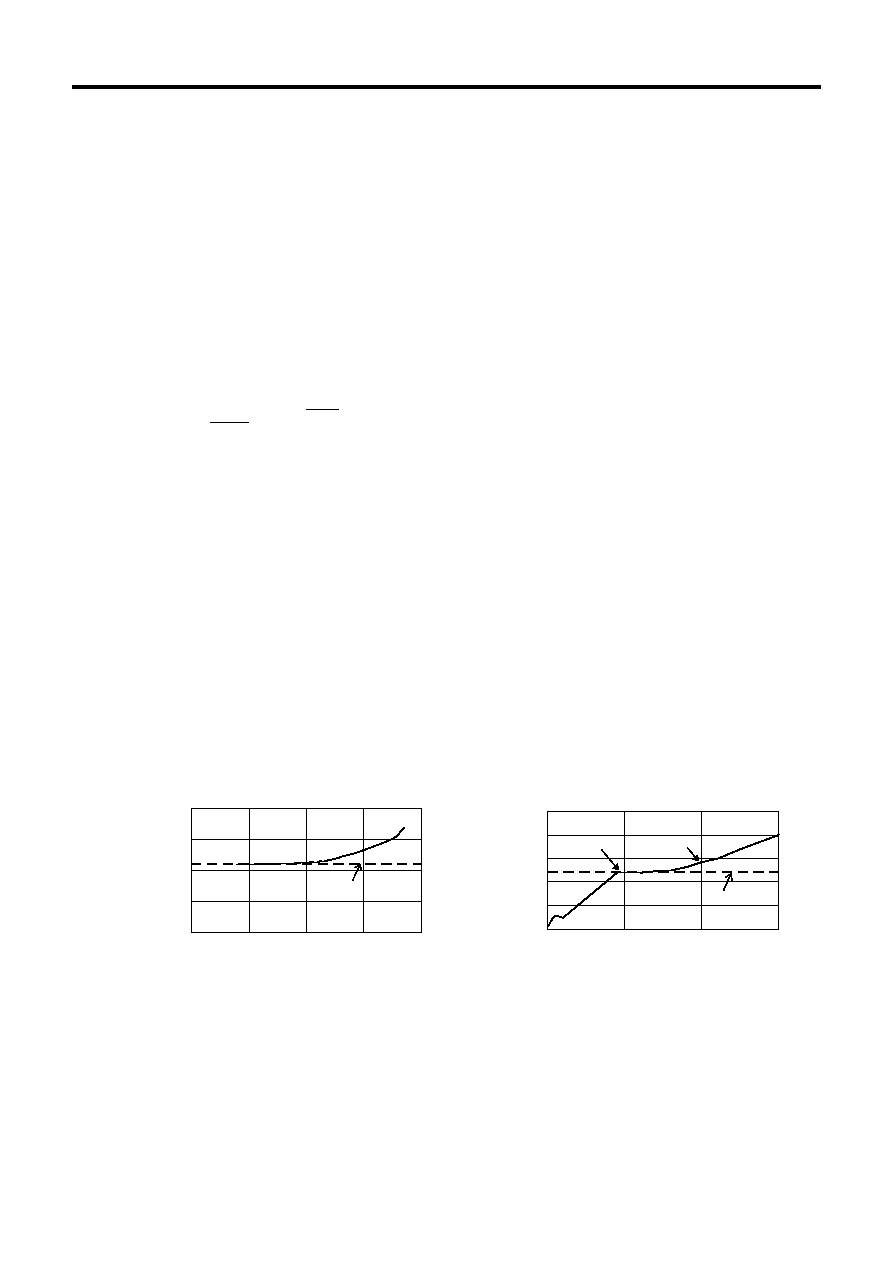
and becomes close to the input voltage. Figure 8 gives an example of the actually measured increase of
the peak current flowing through the coil when the current limit circuit works while the input voltage is
becoming close to the output voltage. Figure 9 shows an example of the actually measured increase of
the peak current flowing through the coil when the output voltage drops and approaches the input
voltage by increasing the output current after the current limit circuit works.
If the current limit circuit is not used, the sensor resistor should be removed and the external transistor
source or emitter and SENSE pin should be connected to V
SS
.
Figure 8
S-8340A50 Rsense
=51 m
0
1
2
3
4
1
2
3
4
5
V
IN
(V)
ILpeak
(A)
(ILpeak measured when the current limit circuit is
activated (V
OUT
begins to fall).)
V
SENSE
/ R
SENSE
Input voltage - Coil peak current
(Coil peak current ILpeak measured)
Figure 9
S-8340A50 VIN=3V Rsense=51m
Output current - Coil peak current
0
1
2
3
4
5
0
1
2
3
Current limit circuit
is activated
V
SENSE
/ R
SENSE
Output current I
OUT
(A)
Coil peak
current Ipk
(A)
Influence of CR
filter

PWM Control & PWM/PFM Control High-Frequency Step-Up Switching Regulator-Controllers
Rev.2.1
_
60
S-8340/8341 Series
Seiko Instruments Inc.
17
Selection of Series Products and Associated External Components
1. Method for selecting series products
The S-8340/41 Series is classified into eight types, according to the way the control systems (PWM and
PWM/PFM-Switched), the different oscillation frequencies, and output voltage setting type are combined
with one with another. Please select the type that best suits your needs by taking advantage of the
features of each type described below.
(1) Control systems:
Two different control systems are available: PWM control system (S-8340 Series) and
PWM/PFM-switched control system (S-8341 Series).
If particular importance is attached to the operation efficiency while the load is on standby --
for example, in an application where the load current heavily varies from that in standby state
as the load starts operating -- a high efficiency will be obtained in standby mode by selecting
the PWM/PFM-switched control system (S-8341 Series).
Moreover, for applications where switching noise poses a serious problem, the PWM control
system (S-8340 Series), in which the switching frequency does not vary with the load current,
is preferable because it can eliminate ripple voltages easily using a filter.
(2) Oscillation frequencies:
Two oscillation frequencies -- 600 kHz (A & B Series) and 300 kHz (C & D Series) -- are
available.
Because of their high oscillation frequency, the products in the A and B Series allow the use
of small-sized inductors since the L value can be reduced. In addition, they can also be used
with small output capacitors. These outstanding features make the A & B Series ideal
products for downsizing the associated equipment.
On the other hand, the C & D Series, having a lower oscillation frequency, are characterized
by a small self-consumption of current and excellent efficiency under light loads. In particular,
the C Series, which employs a PWM/PFM-switched control system, enables the operation
efficiency to be improved drastically when the output load current is approximately 1 mA.
(3) Output voltage setting:
Two different types are available: fixed output type (A & C Series) and external setting type (B
& D Series).
The products (A & C Series) of fixed output type can supply output voltage 2.5 to 6.0 V in 0.1
V steps and assures high precision of
±2.0 % by means of high-resistance and high-precision
internal resistors.
For the products (B & D Series) of external setting type, the output voltage can be adjusted in
the range 2.5 to 6.0 V by adding external resistors R
FB1
and R
FB2
and a capacitor C
FB
.
A temperature gradient can be provided by installing a thermistor in series to R
FB1
and R
FB2
.
The resistance of R
FB1
+ R
FB2
must be equal to or less than 2 M
, and the ratio of R
FB1
to
R
FB2
must be set so that 1.0 V appears at FB pin. Install capacitor C
FB
in parallel to external
resistor R
FB1
to prevent unstable operation, such as output oscillation.
Set C
FB
so that f
=1/(2◊ ◊C
FB
◊R
FB1
) is 0.1 to 20 kHz (normally, 10 kHz).

PWM Control & PWM/PFM Control High-Frequency Step-Up Switching Regulator-Controllers
S-8340/8341 Series
Rev.2.1
_60
Seiko Instruments Inc.
18
Example: V
OUT
=3.0 V, R
FB1
=200 k, R
FB2
=100 k, C
FB
=100 pF
The precision of the output voltage V
OUT
set with resistors R
FB1
and R
FB2
is affected by the
precision of the voltage at FB pin (1 V
±2.0 %), the absolute precision of external resistors
R
FB1
and R
FB2
, the current input to FB pin and IC power supply voltage V
DD
.
When it is assumed that the FB pin input current is 0 nA, the maximum absolute value
variations of external resistors R
FB1
and R
FB2
are R
FB1
max. and R
FB2
max., the minimum
absolute value variations of external resistors R
FB1
and R
FB2
are R
FB1
min. and R
FB2
min., and
the shift of the output voltage due to dependence of voltage on V
DD
is
V, the minimum value
V
OUT
min. and maximum value V
OUT
max. of variations of output voltage V
OUT
are expressed
by the following formulas:
V
min.
1
R min.
R max.
0.98
V[V]
OUT
FB1
FB2
=
+
◊
-
V
max.
1
R max.
R min.
1.02
V[V]
OUT
FB1
FB2
=
+
◊
+
The precision of output voltage V
OUT
cannot be made lower than the IC output voltage
precision (V
OUT
±2.0 %) without adjusting external resistors R
FB1
and R
FB2
. The smaller
R
FB1
/R
FB2
, the less it is affected by the absolute value precision of external resistors R
FB1
and
R
FB2
. The smaller R
FB1
and R
FB2
, the less it is affected by the input current at FB pin.
To reduce the influence of input current at FB pin which effects variations of output voltage
V
OUT
, it is necessary to make the external resistor R
FB2
value sufficiently lower than the input
impedance at FB pin (1 V/50 nA
=20 M max.)
Reactive current flows through external resistors R
FB1
and R
FB2
. If the reactive current value
can not be ignored with respect to the actual load current, efficiency decreases. Therefore,
the resistance of external resistors R
FB1
and R
FB2
should be sufficiently high.
If the resistance of external resistors R
FB1
and R
FB2
is too high (1 M
or more), it is likely to
be affected by external noise, and therefore, we recommend that you evaluate it by testing
performance with the actual equipment.
Since the precision of output voltage V
OUT
and reactive current must be traded off, they must
be considered according to application requirements.
PWM Control & PWM/PFM Control High-Frequency Step-Up Switching Regulator-Controllers
Rev.2.1
_
60
S-8340/8341 Series
Seiko Instruments Inc.
19
Note:
Connect IC power pin VDD to VOUT for both fixed output type and external setting type as in the standard circuit
shown on pages 22 and 23. If VDD is inevitably taken from input voltage VIN or other power source, instead of VOUT,
V
DD
must be raised to 2.5 V or higher within the soft-start time (3.0 ms: A & B Series, 6.0 ms: C & D Series).
If VDD pin is connected to VOUT, input voltage V
IN
can be increased slowly without any problems.
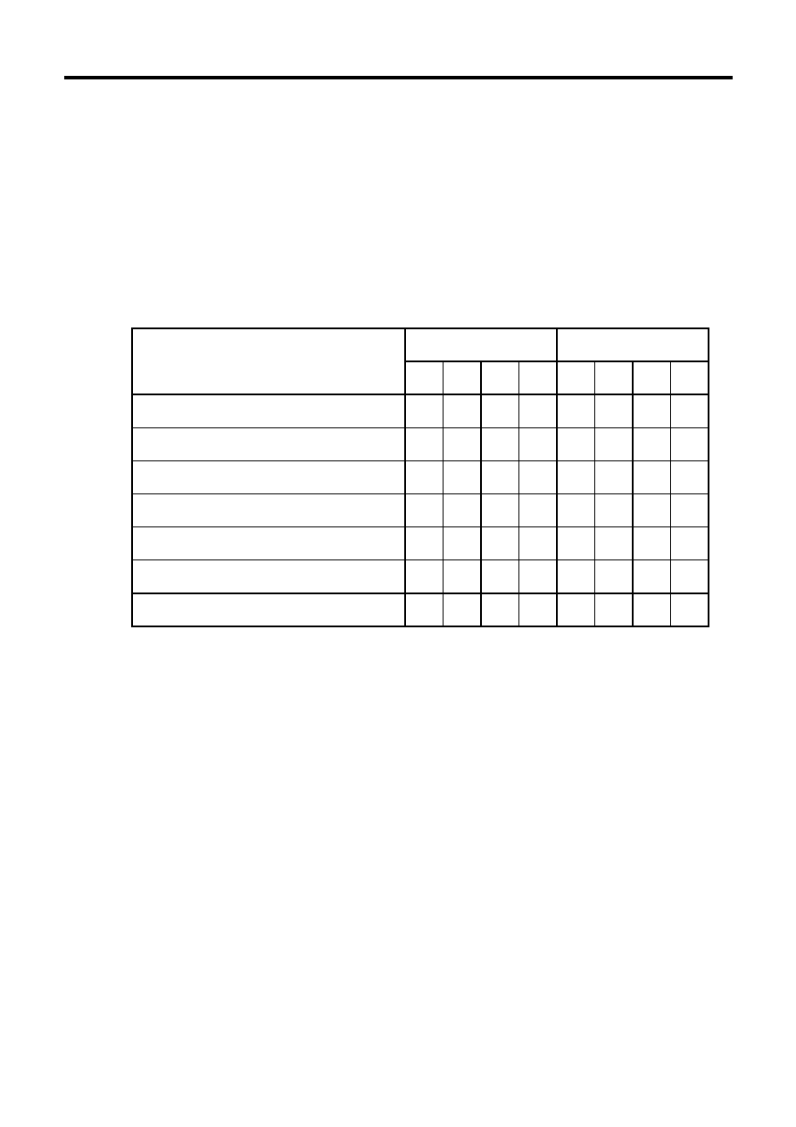
The table below provides a rough guide for selecting a product type depending on the
requirements of the application. Choose the product that gives you the largest number of circles
(O).
Table 1
S-8340
S-8341
A
B
C
D
A
B
C
D
The set output voltage is 6 V or less
Set an output voltage freely
The efficiency under light loads(1mA approx.) is an
important factor
To be operated with a medium load current (200 mA
class)
To be operated with a high load current (1 A class)
It is important to have a low-ripple voltage
Importance is attached to the downsizing of external
components
The symbol "
" denotes an indispensable condition, while the symbol " " indicates that the
corresponding series has superiority in that aspect. The symbol " " indicates particularly high
superiority.
2. Inductor
The inductance value greatly affects the maximum output current I
OUT
and the efficiency
.
As the L-value is reduced gradually, the peak current Ipk increases, to finally reach the maximum output
current I
OUT
when the L-value has fallen to a certain point. If the L-value is made even smaller, I
OUT
will
begin decreasing because the current drive capacity of the switching transistor becomes insufficient.
Conversely, as the L-value is augmented, the loss due to Ipk in the switching transistor will decrease
until the efficiency is maximized at a certain L-value. If the L-value is made even larger, the loss due to
the series resistance of the inductor will increase to the detriment of the efficiency.

PWM Control & PWM/PFM Control High-Frequency Step-Up Switching Regulator-Controllers
S-8340/8341 Series
Rev.2.1
_60
Seiko Instruments Inc.
20
If the L-value is increased in an S-8340/41 Series product, the output voltage may turn unstable in some
cases, depending on the conditions of the input voltage, output voltage, and the load current. Perform
thorough evaluations under the conditions of actual service and decide on an optimum L-value. An L
value should be selected from 2.2 to 22
µH for A & B Series and from 4.7 to 47 µH for C & D Series.
In many applications, selecting a value of A/B Series 5 to 10
µH and C/D Series 10 to 22 µH will allow a
S-8340/41 Series product to yield its best characteristics in a well balanced manner.
When choosing an inductor, pay attention to its allowable current, since a current applied in excess of
the allowable value will cause the inductor to produce magnetic saturation, leading to a marked decline
in efficiency.
Therefore, select an inductor in which the peak current Ipk will not surpass its allowable current at any
moment. The peak current Ipk is represented by the following equation in non-continuous operation
mode:
I
PK
=
2 I
V
V
V
fosc
OUT
OUT
F
IN
(
)
L
◊
◊
+
-
◊
Where fosc is the oscillation frequency, L the inductance value of the inductor, and V
F
the forward
voltage of the diode (appropriate 0.4 V).
For example, if a power supply with input voltage V
IN
=3 V, output voltage V
OUT
=5 V, and load current
I
OUT
=30 mA is used, fosc=600 kHz when S-8340A50AFT is used. When 10 µH is selected for the L
value, I
PK
=155 mA from the above formula. Therefore, select an inductor with a permissible current of
155 mA or higher for the L value of 10
µH.
3. Diode
The diode to be externally coupled to the IC should be a type that meets the following conditions:
Its forward voltage is low (Schottky barrier diode recommended).
Its switching speed is high (50 ns max.).
Its reverse direction breakdown voltage is higher than V
OUT
+ V
F
.
Its current rating is higher than I
PK
.
4. Capacitors (C
IN
, C
L
)
The capacitor inserted on the input side (C
IN
) serves to lower the power impedance and to average the
input current for better efficiency. Select the C
IN
-value according to the impedance of the power supplied.
As a rough rule of thumb, you should use a value of 47 to 100
µF, although the actual value will depend
on the impedance of the power in use and the load current value.
If the input voltage is extremely high or load current is extremely large, the output voltage of the S-
8340/41 Series may become unstable. The unstable range can be narrowed, however, by selecting an
output side capacitor (C
L
) with a large capacitance. If a capacitor with high ESR (Equivalent Series
Resistance), such as an aluminum electrolytic capacitor, or with low ESR, such as a ceramic capacitor,
the unstable range widens. Thus, a tantalum electrolytic capacitor is recommended. We recommend
that you evaluate it by testing performance with the actual equipment.
The capacity should be 47 to 200
µF and ESR should be 40 to 270 m as a recommended yardstick.
5. External Switching Transistor
The S-8340/41 Series can be operated with an external switching transistor of the enhancement (Nch)
MOS FET type or bipolar (NPN) type.
5.1 Enhancement MOS FET
The EXT pin of the S-8340/41 Series is capable of directly driving a Nch power MOS FET.
When a Nch power MOS FET is chosen, because it has a higher switching speed than a NPN type
bipolar transistor and because power losses due to the presence of a base current are avoided,
efficiency will be 2 to 3% higher than NPN type bipolar transistor.

PWM Control & PWM/PFM Control High-Frequency Step-Up Switching Regulator-Controllers
Rev.2.1
_
60
S-8340/8341 Series
Seiko Instruments Inc.
21
Since a large current may flow at power on when a certain type of MOS FET is selected, we recommend
that you evaluate it by testing performance with the actual equipment. The gate capacity of the MOS
FET to be used should be 1200 pF or less.
The important parameters to be kept in mind in selecting a Nch power MOS FET include the threshold
voltage, breakdown voltage between gate and source, breakdown voltage between drain and source,
total gate capacity, on-resistance, and the current rating.
The EXT pin swings from voltage V
DD
over to voltage V
SS
. If the V
DD
voltage is low, a MOS FET with a
low threshold voltage has to be used so that the MOS FET will come on as required. If, conversely, the
V
DD
voltage is high, select a MOS FET whose gate-source breakdown voltage is higher than the V
DD
voltage by at least several volts.
Since the V
OUT
+V
F
voltage is applied between the drain and source of the MOS FET during a step-up
operation, the breakdown voltage between the drain and source should be at least several volts higher
than the V
OUT
+V
F
voltage. The total gate capacity and the on-resistance affect the efficiency.
The power loss for charging and discharging the gate capacity by switching operation will increase, when
the total gate capacity becomes larger and the input voltage rises higher. Therefore the gate capacity
affects the efficiency of power in a low load current region. If the efficiency under light loads is a matter
of particular concern, select a MOS FET with a small total gate capacity.
In regions where the load current is high, the efficiency is affected by power losses caused due to the
on-resistance of the MOS FET. Therefore, if the efficiency under heavy loads is particularly important for
your application, choose a MOS FET with an resistance of lowest as possible.
As for the current rating, select a MOS FET whose maximum continuous drain current rating is higher
than the peak current I
PK
.
5.2 Bipolar NPN
Figure 13 and 14 shows a sample circuit diagram using Sanyo 2SD1628G for the bipolar transistor
(NPN). The driving capacity for increasing the output current by means of a bipolar transistor is
determined by the h
FE
-value and the Rb-value of that bipolar transistor.
The R
b
-value is given by the following equation:
R
b
=
V
0.7
Ib
DD
-
-
0 4
.
I
EXTH
Find the necessary base current Ib using the h
FE
-value of bipolar transistor by the equation, I
b
= I
PK
/h
FE
,
and select a smaller R
b
-value.
A small R
b
-value will certainly contribute to increasing the output current, but it will also adversely affect
the efficiency. Moreover, in practice, a current may flow as the pulses or a voltage drop may take place
due to the wiring resistance or some other reason. Determine an optimum value through
experimentation.
In addition, if speed-up capacitor C
b
is inserted in parallel with resistance R
b
, as shown in Figure 12 and
13, the switching loss will be reduced, leading to a higher efficiency.
Select a C
b
-value by using the following equation as a guide:
C
b
1
2
R
fosc 0.1
b
◊
◊
◊
However, the practically-reasonable C
b
value differs depending upon the characteristics of the bipolar
transistor. Optimize the C
b
value based on the experiment result.

PWM Control & PWM/PFM Control High-Frequency Step-Up Switching Regulator-Controllers
S-8340/8341 Series
Rev.2.1
_60
Seiko Instruments Inc.
22
Standard Circuits
(1) Using a Nch MOS-FET transistor:
VSS
V
OUT
VOUT
SD
R
S
R2
R1
C
S
C
C
C
L
ON /OFF
PWM, PWM/PFM
switching control
circuit
Phase
compensation
circuit
Triangular wave
oscillation circuit
VDD
L
EXT
Voltage/current
reference
Power-off
circuit
V
IN
C
VREF
1 point ground
C
SS
Nch Power
MOS FET
Soft-start
circuit
IC internal power
supply
120mV
R
SENSE
SENSE
PWM comparator
Error amplifier
V
REF
=
=
=
=1.0 V
+
CSS
CVREF
Figure 10 Block diagram <Output voltage fixed output type>
SD
ON /OFF
PWM, PWM/PFM
switching control
circuit
Phase
compensation
circuit
Triangular wave
oscillation circuit
VDD
L
EXT
Voltage/current
reference
Power-off
circuit
V
IN
C
VREF
1 point ground
C
SS
Nch Power
MOS FET
Soft-start
circuit
IC internal power
supply
120mV
R
SENSE
SENSE
PWM comparator
Error amplifier
V
REF
=
=
=
=1.0 V
+
V
OUT
FB
VSS
C
FB
R
S
C
S
C
L
R
FB1
R
FB2
CSS
CVREF
Figure 11 Block diagram <Output voltage external setting type>
PWM Control & PWM/PFM Control High-Frequency Step-Up Switching Regulator-Controllers
Rev.2.1
_
60
S-8340/8341 Series
Seiko Instruments Inc.
23
(2) Using a bipolar transistor
VSS
V
OUT
VOUT
SD
C
S
R
S
R1
R2
C
C
C
L
ON /OFF
PWM/PFM switching
control circuit
Phase
compensation
circuit
Triangular wave
oscillation circuit
VDD
L
C
b
EXT
Voltage/current
reference
Power-off
circuit
V
IN
C
VREF
1 point ground
C
SS
NPN
bipolar
Soft-start
circuit
IC internal power
supply
120 mV
R
SENSE
SENSE
PWM comparator
Error amplifier
V
REF
=
=
=
=1.0 V
+
CSS
CVREF
Figure 12 Block diagram <Output voltage fixed output type>
R
S
C
S
SD
ON /OFF
PWM, PWM/PFM
switching control
circuit
Phase
compensation
circuit
Triangular wave
oscillation circuit
VDD
L
EXT
Voltage/current
reference
Power-off
circuit
V
IN
1 point ground
C
VREF
C
SS
NPN
bipolar
Soft-start
circuit
IC internal power
supply
120 mV
R
SENSE
SENSE
PWMcomparator
Error amplifier
V
REF
=
=
=
=1.0 V
+
V
OUT
FB
VSS
C
FB
C
L
R
FB1
R
FB2
C
b
CSS
CVREF
Figure 13 Block diagram <Output voltage external setting type>
Precautions
Install the external capacitors, diode, coil, and other peripheral components as close to the IC as
possible, and secure grounding at a single location.
Any switching regulator intrinsically produces a ripple voltage and spike noise, which are largely dictated
by the coil and capacitors in use. When designing a circuit, first test them on actual power equipment.
Make sure that dissipation of the switching transistor will not surpass the allowable power dissipation of
the package. (especially at the time of high temperature)

PWM Control & PWM/PFM Control High-Frequency Step-Up Switching Regulator-Controllers
S-8340/8341 Series
Rev.2.1
_60
Seiko Instruments Inc.
24
400
100
200
300
0
0
50
100
150
Power
dissipation
P
D
(mW)
Temperature Ta (
∞C)
Figure 14 Power dissipation of an 8-Pin TSSOP Package (Free-Air)
To stabilize operation, use a capacitor with a low ESR as a bypass capacitor between VDD and VSS of
the IC, and install and wire it with a short distance and a low impedance. Connect C
VREF
to VSS.
The main circuit of the IC operates on the internal power supply connected to the CVREF pin. C
VREF
is a
bypass capacitor that stabilizes the internal power supply. Use a 0.01-1
µF ceramic capacitor as C
VREF
and install and wire it to assure a short distance and a low impedance.
Do not apply an electrostatic discharge to this IC that exceeds the performance ratings of the built-in
electrostatic protection circuit.
Seiko Instruments Inc. shall not be responsible for any patent infringement by products including the S-
8340/8341 Series in connection with the method of using the S-8340/8341 Series in such products, the
product specifications or the country of destination thereof.
PWM Control & PWM/PFM Control High-Frequency Step-Up Switching Regulator-Controllers
Rev.2.1
_
60
S-8340/8341 Series
Seiko Instruments Inc.
25
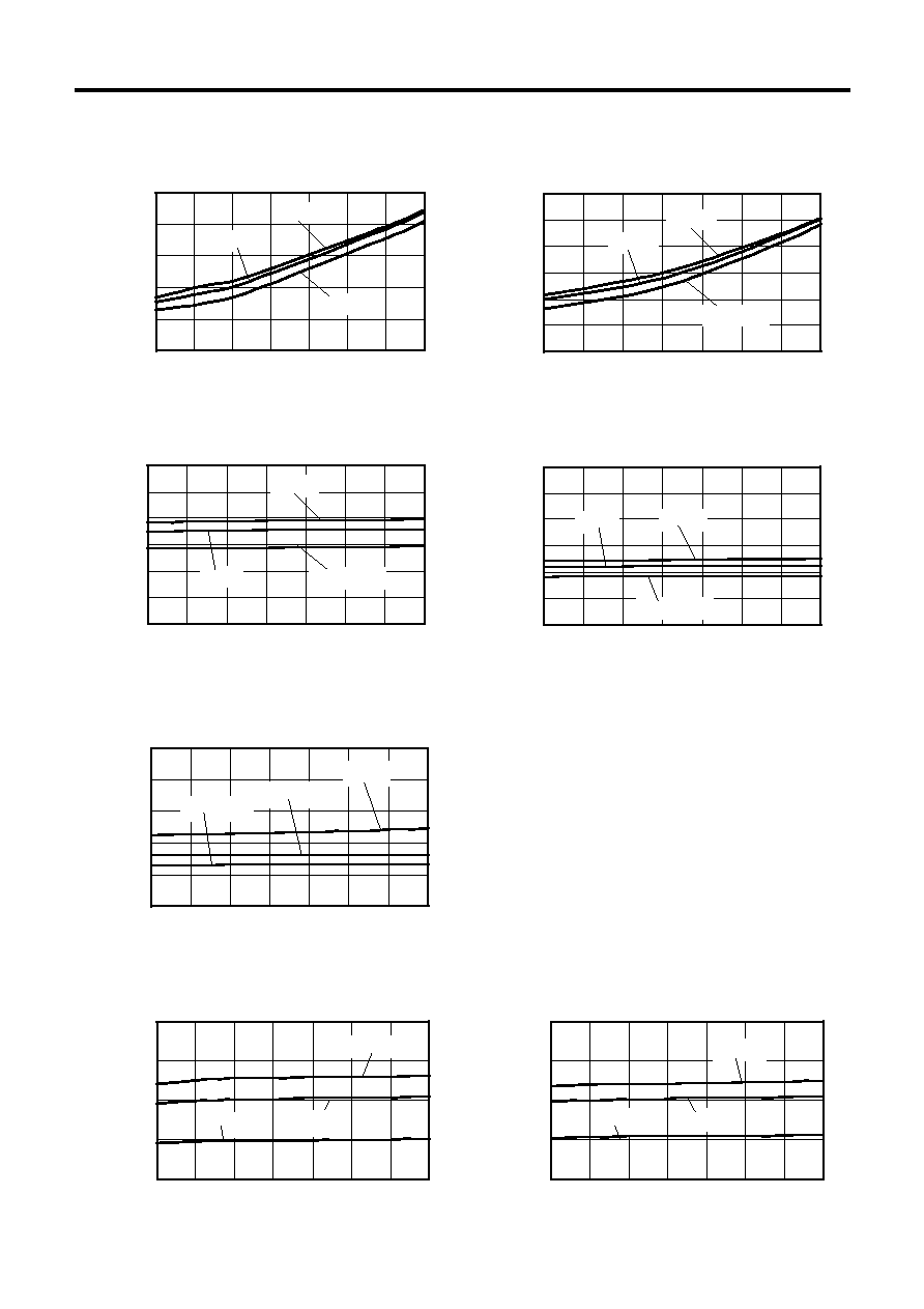
Characteristics of Major Items (All data represents typical values):
(1) I
SS
1--V
DD
S-8340A33A(fosc:600 kHz)
0
200
400
600
800
1000
2.5
3.0
3.5
4.0
4.5
5.0
5.5
6.0
V
DD
(V)
I
SS1
(
µA)
25∞C
85∞C
Ta
=-40∞
S-8340C33A(fosc:300 kHz)
0
100
200
300
400
500
600
2.5
3.0
3.5
4.0
4.5
5.0
5.5
6.0
V
DD
(V)
I
SS1
(
µA)
25∞C
85∞C
Ta
=-40∞
(2) I
SS
2--V
DD
S-8340A33A(fosc:600 kHz)
0
50
100
150
200
250
300
2.5
3.0
3.5
4.0
4.5
5.0
5.5
6.0
V
DD
(V)
I
SS2
(
µA)
25∞C
85∞C
Ta
=-40∞C
S-8340C33A(fosc:300 kHz)
0
50
100
150
200
250
300
2.5
3.0
3.5
4.0
4.5
5.0
5.5
6.0
V
DD
(V)
I
SS2
(
µA)
25∞C
85∞C
Ta
=-40∞C
(3) I
SSS
--V
DD
S-8340A33A(fosc:600 kHz) / S-8340C33A(fosc:300 kHz)
0.0
0.2
0.4
0.6
0.8
1.0
2.5
3.0
3.5
4.0
4.5
5.0
5.5
6.0
V
DD
(V)
I
SSS
(
µA)
25∞C
85∞C
Ta
=-40∞C
(4) fosc--V
DD
S-8340A33A(fosc:600 kHz)
400
500
600
700
800
2.5
3.0
3.5
4.0
4.5
5.0
5.5
6.0
V
DD
(V)
fosc
(kHz)
25∞C
85∞C
Ta
=-40∞C
S-8340C33A(fosc:300 kHz)
200
250
300
350
400
2.5
3.0
3.5
4.0
4.5
5.0
5.5
6.0
V
DD
(V)
fosc
(kHz)
25∞C
85∞C
Ta
=-40∞C

PWM Control & PWM/PFM Control High-Frequency Step-Up Switching Regulator-Controllers
S-8340/8341 Series
Rev.2.1
_60
Seiko Instruments Inc.
26
(5) I
EXTH
--V
DD
(6) I
EXTL
--V
DD
-60
-50
-40
-30
-20
-10
0
2.5
3.0
3.5
4.0
4.5
5.0
5.5
6.0
V
DD
(V)
I
EXTH
(mA)
25∞C
85∞C
Ta
=-40∞C
S-8340A33A(fosc:600 kHz) / S-8340C33A(fosc:300 kHz) S-8340A33A(fosc:600 kHz) / S-8340C33A(fosc:300 kHz)
0
20
40
60
80
100
120
140
2.5
3.0
3.5
4.0
4.5
5.0
5.5
6.0
V
DD
(V)
I
EXTL
(mA)
25∞C
85∞C
Ta
=-40∞C
(7) T
SS
--V
DD
S-8340A33A(fosc:600 kHz)
0
5
10
15
20
2.5
3.0
3.5
4.0
4.5
5.0
5.5
6.0
V
DD
(V)
T
SS
(ms)
25∞C
Ta
=-40∞C
85∞C
S-8340C33A(fosc:300 kHz)
0
10
20
30
40
2.5
3.0
3.5
4.0
4.5
5.0
5.5
6.0
V
DD
(V)
T
SS
(ms)
25∞C
Ta
=-40∞C
85∞C
(8) V
SH
--V
DD
(9) VSL--VDD
S-8340A33A(fosc:600 kHz) / S-8340C33A(fosc:300 kHz)
0.0
0.2
0.4
0.6
0.8
1.0
2.5
3.0
3.5
4.0
4.5
5.0
5.5
6.0
V
DD
(V)
V
SH
(V)
25∞C
85∞C
Ta
=-40∞C
S-8340A33A(fosc:600 kHz) / S-8340C33A(fosc:300 kHz)
0.0
0.2
0.4
0.6
0.8
1.0
2.5
3.0
3.5
4.0
4.5
5.0
5.5
6.0
V
DD
(V)
V
SL
(V)
25∞C
85∞C
Ta
=-40∞C
(10) V
OUT
--V
DD
2.40
2.42
2.44
2.46
2.48
2.50
2.52
2.54
2.5
3.0
3.5
4.0
4.5
5.0
5.5
6.0
V
DD
(V)
V
OUT
(V)
25∞C
85∞C
Ta
=-40∞C
S-8340A25A(fosc:600 kHz) / S-8340C25A(fosc:300 kHz)
3.20
3.22
3.24
3.26
3.28
3.30
3.32
3.34
2.5
3.0
3.5
4.0
4.5
5.0
5.5
6.0
V
DD
(V)
V
OUT
(V)
25∞C
85∞C
Ta
=-40∞C
S-8340A33A(fosc:600 kHz) / S-8340C33A(fosc:300 kHz)

PWM Control & PWM/PFM Control High-Frequency Step-Up Switching Regulator-Controllers
Rev.2.1
_
60
S-8340/8341 Series
Seiko Instruments Inc.
27
(11) V
OUT
--V
DD
(12) V
ST
--Ta
4.90
4.92
4.94
4.96
4.98
5.00
5.02
5.04
2.5
3.0
3.5
4.0
4.5
5.0
5.5
6.0
V
DD
(V)
V
OUT
(V)
25∞C
85∞C
Ta
=-40∞C
S-8340A50A(fosc:600 kHz) / S-8340C50A(fosc:300 kHz)
0.4
0.5
0.6
0.7
0.8
0.9
1.0
-40
-20
0
20
40
60
80
Ta(∞C)
V
ST
(V)
S-8340A33A(fosc:600 kHz) / S-8340C33A(fosc:300 kHz)
(13) MaxDuty--V
DD
79
80
81
82
83
84
85
2.5
3.0
3.5
4.0
4.5
5.0
5.5
6.0
V
DD
(V)
Max
Duty
(
%)
85∞C
25∞C
Ta
=-40∞C
S-8340A33A(fosc:600 kHz) / S-8340C33A(fosc:300 kHz)
(14) PFMDuty--V
DD
S-8341A33A(fosc:600 kHz)
24
25
26
27
28
29
30
2.5
3.0
3.5
4.0
4.5
5.0
5.5
6.0
V
DD
(V)
PFM
Duty
(
%)
85∞C
25∞C
Ta
=-40∞C
S-8341C33A(fosc:300 kHz)
18
19
20
21
22
23
24
2.5
3.0
3.5
4.0
4.5
5.0
5.5
6.0
V
DD
(V)
PFM
Duty
(
%)
85∞C
25∞C
Ta
=-40∞C
(15) V
SENSE
--V
DD
105
110
115
120
125
130
135
2.5
3.0
3.5
4.0
4.5
5.0
5.5
6.0
V
DD
(V)
V
SENSE
(mV)
85∞C
25∞C
Ta
=-40∞C
S-8340A33A(fosc:600 kHz) / S-8340C33A(fosc:300 kHz)
PWM Control & PWM/PFM Control High-Frequency Step-Up Switching Regulator-Controllers
S-8340/8341 Series
Rev.2.1
_60
Seiko Instruments Inc.
28
Transient Response Characteristics:
1. Power-On
(1) S-8340A33AFT, fosc
=
=
=
=600 kHz, Ta====25 ∞∞∞∞C, All data represents typical values
V
IN
=01.98 V, I
OUT
=1 mA
TIME(2 ms/div)
V
OUT
(1 V/div)
3 V
0 V
3 V
0 V
V
IN
(1 V/div)
V
IN
=01.98 V, I
OUT
=200 mA
TIME(2 ms/div)
V
OUT
(1 V/div)
3 V
0 V
3 V
0 V
V
IN
(1 V/div)
(2) S-8340C33AFT, fosc
=
=
=
=300 kHz, Ta====25 ∞∞∞∞C, All data represents typical values
V
IN
=01.98 V, I
OUT
=1 mA
TIME(4 ms/div)
V
OUT
(1 V/div)
3 V
0 V
3 V
0 V
V
IN
(1 V/div)
V
IN
=01.98 V, I
OUT
=200 mA
TIME(4 ms/div)
V
OUT
(1 V/div)
3 V
0 V
3 V
0 V
V
IN
(1 V/div)
2. Power-Off Pin Response
(1) S-8340A33AFT, fosc
=
=
=
=600 kHz, Ta====25 ∞∞∞∞C, All data represents typical values
ON/OFF
=01.98 V, I
OUT
=1 mA
TIME(2 ms/div)
V
OUT
(1 V/div)
3 V
0 V
3 V
0 V
V
ON/OFF
(1 V/div)
ON/OFF
=01.98 V, I
OUT
=200 mA
TIME(2 ms/div)
V
OUT
(1 V/div)
3 V
0 V
3 V
0 V
V
ON/OFF
(1 V/div)
(2) S-8340C33AFT, fosc=300kHz, Ta=25
∞
∞
∞
∞C, All data represents typical values
ON/OFF
=01.98 V, I
OUT
=1 mA
TIME(4 ms/div)
V
OUT
(1 V/div)
3 V
0 V
3 V
0 V
V
ON/OFF
(1 V/div)
ON/OFF
=01.98 V, I
OUT
=200 mA
TIME(4 ms/div)
V
OUT
(1 V/div)
3 V
0 V
3 V
0 V
V
ON/OFF
(1 V/div)
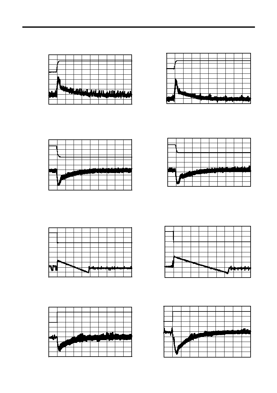
PWM Control & PWM/PFM Control High-Frequency Step-Up Switching Regulator-Controllers
Rev.2.1
_
60
S-8340/8341 Series
Seiko Instruments Inc.
29
3. Supply Voltage Variation
(1) S-8340A33AFT,fosc=600kHz
S-8340C33AFT,fosc=300kHz
V
IN
=1.982.64 V, I
OUT
=100 mA
TIME(0.2 ms/div)
V
OUT
(0.02 V/div)
2.64 V
1.98 V
V
IN
(0.3 V/div)
V
IN
=1.982.64 V, I
OUT
=100 mA
TIME(0.2 ms/div)
2.64 V
1.98 V
V
IN
(0.4 V/div)
V
OUT
(0.02 V/div)
(2) S-8340A33AFT,fosc=600kHz
S-8340C33AFT,fosc=300kHz
V
IN
=2.641.98 V, I
OUT
=100 mA
TIME(0.2 ms/div)
2.64 V
1.98 V
V
IN
(0.3 V/div)
V
OUT
(0.02 V/div)
V
IN
=2.641.98 V, I
OUT
=100 mA
TIME(0.2 ms/div)
2.64 V
1.98 V
V
IN
(0.4 V/div)
V
OUT
(0.02 V/div)
4. Load Variation
(1) S-8340A33AFT,fosc
=
=
=
=600 kHz
S-8340C33AFT,fosc
=
=
=
=300 kHz
V
IN
=1.98V, I
OUT
=100 mA100 µA
TIME(4 ms/div)
V
OUT
(0.02 V/div)
100 mA
100
µA
I
OUT
V
IN
=1.98 V, I
OUT
=100 mA100 µA
TIME(4 ms/div)
100 mA
100
µA
I
OUT
V
OUT
0.02 V/div)
(2) S-8340A33AFT,fosc
=
=
=
=600 kHz
S-8340C33AFT,fosc
=
=
=
=300 kHz
V
IN
=1.98 V, I
OUT
=100 µA100 mA
TIME(0.2 ms/div)
V
OUT
(0.02 V/div)
100 mA
100
µA
I
OUT
TIME(0.2 ms/div)
100 mA
100
µA
I
OUT
V
IN
=1.98 V, I
OUT
=100 µA100 mA
V
OUT
(0.02/div)
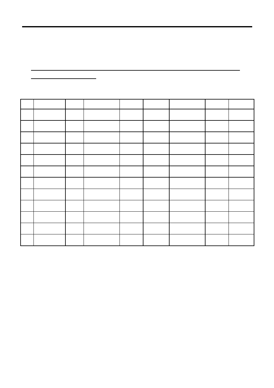
PWM Control & PWM/PFM Control High-Frequency Step-Up Switching Regulator-Controllers
S-8340/8341 Series
Rev.2.1
_60
Seiko Instruments Inc.
30
External Parts Reference Data (All data represents typical values)
This reference data is intended to help you select peripheral components to be externally connected to
the IC. Therefore, this information provides recommendations on external components selected with a
view to accommodating a wide variety of IC applications. Characteristic data is duly indicated in the table
below.
List of external components with efficiency - output current characteristics and output voltage -
output current characteristics
Table 2
A Series (fosc
=
=
=
= 600 kHz)
No.
Product Name
Output
Voltage
Inductor
Transistor
Diode
Output
Capacitor
SENSE
Resistance
Application
(1)
S-8340A25AFT
2.5 V
CDRH5D18/4.1
µH
NDS335N
RB491D
F920J476MB3
◊1
0
(2)
S-8340A25AFT
2.5 V
CDRH124/10
µH
FTS2001
RB081L
-20
F951C476MG1
◊2
0
(3)
S-8341A25AFT
2.5 V
CDRH5D18/4.1
µH
NDS335N
RB491D
F920J476MB3
◊1
0
(4)
S-8341A25AFT
2.5 V
CDRH124/10
µH
FTS2001
RBO81L
-20
F951C476MG1
◊2
0
(5)
S-8340A33AFT
3.3 V
CDRH5D18/4.1
µH
NDS335N
RB491D
F920J476MB3
◊1
0
(6)
S-8340A33AFT
3.3 V
CDRH124/10
µH
FTS2001
RBO81L-20
F951C476MG1
◊2
0
(7)
S-8341A33AFT
3.3 V
CDRH5D18/4.1
µH
NDS335N
RB491D
F920J476MB3
◊1
0
(8)
S-8341A33AFT
3.3 V
CDRH124/10
µH
FTS2001
RBO81L
-20
F951C476MG1
◊2
0
(9)
S-8340A50AFT
5.0 V
CDRH5D18/4.1
µH
NDS335N
RB491D
F951A476MF1
◊1
0
(10)
S-8340A50AFT
5.0 V
CDRH124/10
µH
FTS2001
RBO81L
-20
F951C476MG1
◊2
0
(11)
S-8341A50AFT
5.0 V
CDRH5D18/4.1
µH
NDS335N
RB491D
F951A476MF1
◊1
0
(12)
S-8341A50AFT
5.0 V
CDRH124/10
µH
FTS2001
RBO81L
-20
F951C476MG1
◊2
0
PWM Control & PWM/PFM Control High-Frequency Step-Up Switching Regulator-Controllers
Rev.2.1
_
60
S-8340/8341 Series
Seiko Instruments Inc.
31
Table 3
B Series (fosc
=
=
=
= 300 kHz)
No.
Product Name
Output
Voltage
Inductor
Transistor
Diode
Output
Capacitor
SENSE
Resistance
Application
(13)
S-8340C25AFT
2.5 V
CDRH6D28/10
µH
FDN335N
RB491D
F951C476MG1
◊1
0
(14)
S-8340C25AFT
2.5 V
CDRH124/10
µH
FTS2001
RBO81L
-20
F951C476MG1
◊2
0
(15)
S-8341C25AFT
2.5 V
CDRH6D28/10
µH
FDN335N
RB491D
F951C476MG1
◊1
0
(16)
S-8341C25AFT
2.5 V
CDRH124/10
µH
FTS2001
RBO81L
-20
F951C476MG1
◊2
0
(17)
S-8340C33AFT
3.3 V
CDRH6D28/10
µH
FDN335N
RB491D
F951C476MG1
◊1
0
(18)
S-8340C33AFT
3.3 V
CDRH124/10
µH
FTS2001
RBO81L
-20
F951C476MG1
◊2
0
(19)
S-8341C33AFT
3.3 V
CDRH6D28/10
µH
FDN335N
RB491D
F951C476MG1
◊1
0
(20)
S-8341C33AFT
3.3 V
CDRH124/10
µH
FTS2001
RBO81L
-20
F951C476MG1
◊2
0
(21)
S-8340C50AFT
5.0 V
CDRH6D28/10
µH
FDN335N
RB491D
F951C476MG1
◊1
0
(22)
S-8340C50AFT
5.0 V
CDRH124/10
µH
FTS2001
RBO81L
-20
F951C476MG1
◊2
0
(23)
S-8341C50AFT
5.0 V
CDRH6D28/10
µH
FDN335N
RB491D
F951C476MG1
◊1
0
(24)
S-8341C50AFT
5.0 V
CDRH124/10
µH
FTS2001
RBO81L
-20
F951C476MG1
◊2
0
External components with PFM/PWM-switched input voltage - output current characteristics
Table 4
A Series (fosc
=
=
=
= 600 kHz)
No.
Product Name
Output
Voltage
Inductor
Transistor
Diode
Output
Capacitor
SENSE
Resistance
Application
(25)
S-8341A25AFT
2.5 V
CDRH5D18/4.1
µH
NDS335N
RB491D
F920J476MB3
◊1
0
(26)
S-8341A25AFT
2.5 V
CDRH124/10
µH
FTS2001
RB081L-20
F951C476MG1
◊2
0
(27)
S-8341A33AFT
3.3 V
CDRH5D18/4.1
µH
NDS335N
RB491D
F920J476MB3
◊1
0
(28)
S-8341A33AFT
3.3 V
CDRH124/10
µH
FTS2001
RB081L-20
F951C476MG1
◊2
0
(29)
S-8341A50AFT
5.0 V
CDRH5D18/4.1
µH
NDS335N
RB491D
F951A476MF1
◊1
0
(30)
S-8341A50AFT
5.0 V
CDRH124/10
µH
FTS2001
RB081L-20
F951C476MG1
◊2
0
PWM Control & PWM/PFM Control High-Frequency Step-Up Switching Regulator-Controllers
S-8340/8341 Series
Rev.2.1
_60
Seiko Instruments Inc.
32
C Series (fosc
=
=
=
= 300 kHz)
Table 5
No.
Product Name
Output
Voltage
Inductor
Transistor
Diode
Output
Capacitor
SENSE
Resistance
Application
(31)
S-8341C25AFT
2.5 V
CDRH6D28/10
µH
FDN335N
RB491D
F951C476MG1
◊1
0
(32)
S-8341C25AFT
2.5 V
CDRH124/10
µH
FTS2001
RBO81L-20
F951C476MG1
◊2
0
(33)
S-8341C33AFT
3.3 V
CDRH6D28/10
µH
FDN335N
RB491D
F951C476MG1
◊1
0
(34)
S-8341C33AFT
3.3 V
CDRH124/10
µH
FTS2001
RBO81L-20
F951C476MG1
◊2
0
(35)
S-8341C50AFT
5.0 V
CDRH6D28/10
µH
FDN335N
RB491D
F951C476MG1
◊1
0
(36)
S-8341C50AFT
5.0 V
CDRH124/10
µH
FTS2001
RBO81L-20
F951C476MG1
◊2
0
External components with ripple - output current characteristics
Table 6
A Series (fosc
=
=
=
= 600 kHz)
No.
Product
Name
Output
Voltage
Inductor
Transistor
Diode
Output
Capacitor
SENSE
Resistance
Application
(37)
S-8340A25AFT
2.5 V
CDRH5D18/4.1
µH
NDS335N
RB491D
F920J476MB3
◊1
F920J476MB3
◊2
0
(38)
S-8340A25AFT
2.5 V
CDRH124/10
µH
FTS2001
RBO81L-20
F951C476MG1
◊2
F951A107MG1
◊2
0
(39)
S-8341A25AFT
2.5 V
CDRH5D18/4.1
µH
NDS335N
RB491D
F920J476MB3
◊1
F920J476MB3
◊2
0
(40)
S-8341A25AFT
2.5 V
CDRH124/10
µH
FTS2001
RBO81L-20
F951C476MG1
◊2
F951A107MG1
◊2
0
(41)
S-8340A33AFT
3.3 V
CDRH5D18/4.1
µH
NDS335N
RB491D
F920J476MB3
◊1
F920J476MB3
◊2
0
(42)
S-8340A33AFT
3.3 V
CDRH124/10
µH
FTS2001
RBO81L-20
F951C476MG1
◊2
F951A107MG1
◊2
0
(43)
S-8341A33AFT
3.3 V
CDRH5D18/4.1
µH
NDS335N
RB491D
F920J476MB3
◊1
F920J476MB3
◊2
0
(44)
S-8341A33AFT
3.3 V
CDRH124/10
µH
FTS2001
RBO81L-20
F951C476MG1
◊2
F951A107MG1
◊2
0
(45)
S-8340A50AFT
5.0 V
CDRH5D18/4.1
µH
NDS335N
RB491D
F951A476MF1
◊1
F951A476MF1
◊2
0
(46)
S-8340A50AFT
5.0 V
CDRH124/10
µH
FTS2001
RBO81L-20
F951C476MG1
◊2
F951A107MG1
◊2
0
(47)
S-8341A50AFT
5.0 V
CDRH5D18/4.1
µH
NDS335N
RB491D
F951A476MF1
◊1
F951A476MF1
◊2
0
(48)
S-8341A50AFT
5.0 V
CDRH124/10
µH
FTS2001
RBO81L-20
F951C476MG1
◊2
F951A107MG1
◊2
0
PWM Control & PWM/PFM Control High-Frequency Step-Up Switching Regulator-Controllers
Rev.2.1
_
60
S-8340/8341 Series
Seiko Instruments Inc.
33
Table 7
C Series (fosc
=
=
=
= 300 kHz)
No.
Product Name
Output
Voltage
Inductor
Transistor
Diode
Output
Capacitor
SENSE
Resistance
Application
(49)
S-8340C25AFT
2.5 V
CDRH6D28/10
µH
FDN335N
RB491D
F951C476MG1
◊1
F951C476MG1
◊2
0
(50)
S-8340C25AFT
2.5 V
CDRH124/10
µH
FTS2001
RBO81L-20
F951C476MG1
◊2
F951A107MG1
◊2
0
(51)
S-8341C25AFT
2.5 V
CDRH6D28/10
µH
FDN335N
RB491D
F951C476MG1
◊1
F951C476MG1
◊2
0
(52)
S-8341C25AFT
2.5 V
CDRH124/10
µH
FTS2001
RBO81L-20
F951C476MG1
◊2
F951A107MG1
◊2
0
(53)
S-8340C33AFT
3.3 V
CDRH6D28/10
µH
FDN335N
RB491D
F951C476MG1
◊1
F951C476MG1
◊2
0
(54)
S-8340C33AFT
3.3 V
CDRH124/10
µH
FTS2001
RBO81L-20
F951C476MG1
◊2
F951A107MG1
◊2
0
(55)
S-8341C33AFT
3.3 V
CDRH6D28/10
µH
FDN335N
RB491D
F951C476MG1
◊1
F951C476MG1
◊2
0
(56)
S-8341C33AFT
3.3 V
CDRH124/10
µH
FTS2001
RBO81L-20
F951C476MG1
◊2
F951A107MG1
◊2
0
(57)
S-8340C50AFT
5.0 V
CDRH6D28/10
µH
FDN335N
RB491D
F951C476MG1
◊1
F951C476MG1
◊2
0
(58)
S-8340C50AFT
5.0 V
CDRH124/10
µH
FTS2001
RBO81L-20
F951C476MG1
◊2
F951A107MG1
◊2
0
(59)
S-8341C50AFT
5.0 V
CDRH6D28/10
µH
FDN335N
RB491D
F951C476MG1
◊1
F951C476MG1
◊2
0
(60)
S-8341C50AFT
5.0 V
CDRH124/10
µH
FTS2001
RBO81L-20
F951C476MG1
◊2
F951A107MG1
◊2
0
Applications
CDRH5D18
+ NDS335N + RB491D -> Small thin components with a height of 2 mm or less (Maximum current of the
external component is set to 1.7 A.)
CDRH124
+ FTS2001 + RBO81L-20 -> Large load current (Maximum current of the external component is set to 4.5
A.)
CDRH6D28
+ FDN335N + RB491D -> Selection for high efficiency with a height of 3 mm or less.
CDRH124
+ FTS2001 + RBO81L-20 -> Selection to bring out the maximum load current drivability.
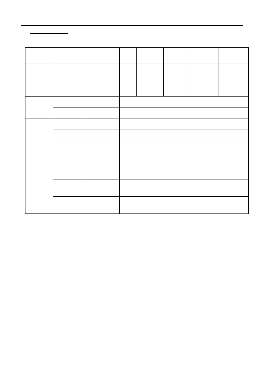
PWM Control & PWM/PFM Control High-Frequency Step-Up Switching Regulator-Controllers
S-8340/8341 Series
Rev.2.1
_60
Seiko Instruments Inc.
34
Performance Data
Table 8
Component
Product
Name
Manufacturer's
Name
L-
Value
DC
Resistance
Max.
Allowable
Current
Dia.
Height
CDRH5D18
Sumida
4.1
µH
42 m
typ.
57 m
max.
1.95 A
5. 7 mm typ.
6.0 mm max.
1. 8 mm typ.
2.0 mm max.
Inductor
CDRH124
Sumida
10
µH
28 m
max.
4.5 A
12. 0 mm typ.
12.3 mm max.
4.5 mm max.
CDRH6D28
Sumida
10
µH
48 m
typ.
65 m
max.
1.70 A
6.7 mm typ.
7.0 mm max.
3.0 mm max.
Diode
RB491D
ROHM
Forward current 1.0 A (When VF
=0.45 V), Vrm=25 V
RB081L
-20
ROHM
Forward current 5.0 A (When VF
=0.45 V), Vrm=25 V
F951C476MG1
Nichicon
47
µF, 16 V, 5.5 ◊ 4.8◊ 2.3 mm max., ESR (official value)=0.08
Output
Capacity
F951A476MF1
Nichicon
47
µF, 10 V, 5.5 ◊ 4.8◊ 2.0 mm max. , ESR (official value)=0.1
(tantalum
electrolytic
F920J476MB3
Nichicon
47
µF, 6.3 V, 3.6 ◊ 3 ◊ 1.2 mm max. , ESR (official value)=0.27
capacitor)
F951A107MG1
Nichicon
100
µF, 10 V, 5.5 ◊ 4.8 ◊ 2.3 mm max. , ESR (official value)=0.08
External
NDS335N*
Fairchild
Vdss
=20 V max., Vgss=8 V max., ID =1.7 A max., Vth=0.5 V to 1 V
Ciss 240 pF typ.
Ron 0.14
max.(Vgs=2.7 V), SOT-23-3 package or equivalent
Transistor
(MOS FET)
FDN335N
Fairchild
Vdss
=20 V max., Vgss=8 V max., ID =1.7 A max., Vth=0.4 V to 1.5 V
Ciss 310 pF typ.
Ron 0.10
max.(Vgs=2.5 V), SOT-23-3 package or equivalent
FTS2001
Sanyo
Vdss
=20 V max., Vgss=8 V max., ID =5 A max., Vth=0.4 V to 1.3 V
Ciss 750 Pf typ.
Ron 46 m
max.(Vgs=2.5 V) , 8-pin TSSOP package
Note:
* Discontinuance of the NDS335N is scheduled. Fairchild recommends FDN335N as a substitute.
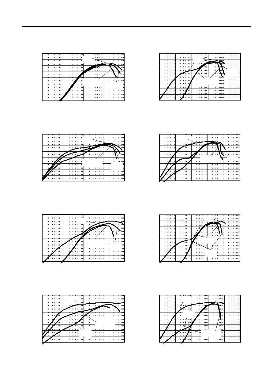
PWM Control & PWM/PFM Control High-Frequency Step-Up Switching Regulator-Controllers
Rev.2.1
_
60
S-8340/8341 Series
Seiko Instruments Inc.
35
1. Efficiency
--Output current I
OUT
Characteristics
(1) S-8340A25AFT
(2) S-8340A25AFT
0.1
1
10
100
1000
20
30
40
50
60
70
80
90
100
I
OUT
(mA)
(
%)
V
IN
=1.2 V
1.5 V
1.8 V
(CDRH5D18/4.1
µH, NDS335N)
20
30
40
50
60
70
80
90
100
(
%)
V
IN
=1.5 V
2.4 V
1.8 V
I
OUT
(mA)
(CDRH124/10
µH, FTS2001)
0.1
1
10
100
1000
10000
(3) S-8341A25AFT
(4) S-8341A25AFT
20
30
40
50
60
70
80
90
100
0.1
1
10
100
1000
(
%)
V
IN
=1.2 V
1.5 V
1.8 V
I
OUT
(mA)
(CDRH5D18/4.1
µH, NDS335N)
20
30
40
50
60
70
80
90
100
(
%)
V
IN
=1.5 V
1.8 V
2.4 V
I
OUT
(mA)
(CDRH124/10
µH, FTS2001)
0.1
1
10
100
1000
10000
(5) S-8340A33AFT
(6) S-8340A33AFT
20
30
40
50
60
70
80
90
100
(
%)
V
IN
=1.2 V
3.0 V
1.8 V
I
OUT
(mA)
(CDRH5D18/4.1
µH, NDS335N)
0.1
1
10
100
1000
20
30
40
50
60
70
80
90
100
(
%)
V
IN
=1.5 V
3.0 V
1.8 V
I
OUT
(mA)
(CDRH124/10
µH, FTS2001)
0.1
1
10
100
1000
10000
(7) S-8341A33AFT
(8) S-8341A33AFT
20
30
40
50
60
70
80
90
100
0.1
1
10
100
1000
(
%)
V
IN
=1.2
3.0 V
1.8 V
I
OUT
(mA)
(CDRH5D18/4.1
µH, NDS335N)
20
30
40
50
60
70
80
90
100
(
%)
V
IN
=1.5 V
3.0 V
1.8 V
I
OUT
(mA)
(CDRH124/10
µH, FTS2001)
0.1
1
10
100
1000
10000
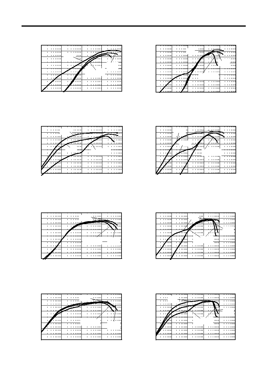
PWM Control & PWM/PFM Control High-Frequency Step-Up Switching Regulator-Controllers
S-8340/8341 Series
Rev.2.1
_60
Seiko Instruments Inc.
36
(9) S-8340A50AFT
(10) S-8340A50AFT
20
30
40
50
60
70
80
90
100
(
%)
V
IN
=1.8 V
4.5 V
3.0 V
I
OUT
(mA)
(CDRH5D18/4.1
µH, NDS335N)
0.1
1
10
100
1000
20
30
40
50
60
70
80
90
100
(
%)
V
IN
=1.8 V
4.5 V
3.0 V
I
OUT
(mA)
(CDRH124/10
µH, FTS2001)
0.1
1
10
100
1000
10000
(11) S-8341A50AFT
(12) S-8341A50AFT
20
30
40
50
60
70
80
90
100
0.1
1
10
100
1000
(
%)
V
IN
=1.8 V
4.5 V
3.0 V
I
OUT
(mA)
(CDRH5D18/4.1
µH, NDS335N)
20
30
40
50
60
70
80
90
100
(
%)
V
IN
=1.8 V
4.5 V
3.0 V
I
OUT
(mA)
I
OUT
(mA)
(CDRH124/10
µH, FTS2001)
0.1
1
10
100
1000
10000
(13) S-8340C25AFT
(14) S-8340C25AFT
20
30
40
50
60
70
80
90
100
I
OUT
(mA)
(
%)
V
IN
=1.2 V
1.5 V
1.8 V
(CDRH6D28/10
µH, FDN335N)
0.1
1
10
100
1000
20
30
40
50
60
70
80
90
100
(
%)
V
IN
=1.5 V
2.4 V
1.8 V
I
OUT
(mA)
(CDRH124/10
µH, FTS2001)
0.1
1
10
100
1000
10000
(15) S-8341C25AFT
(16) S-8341C25AFT
20
30
40
50
60
70
80
90
100
0.1
1
10
100
1000
I
OUT
(mA)
(
%)
V
IN
=1.2 V
1.5 V
1.8 V
(CDRH6D28/10
µH, FDN335N)
20
30
40
50
60
70
80
90
100
0.1
1
10
100
1000
10000
(
%)
V
IN
=1.5 V
2.4 V
1.8 V
I
OUT
(mA)
(CDRH124/10
µH, FTS2001)
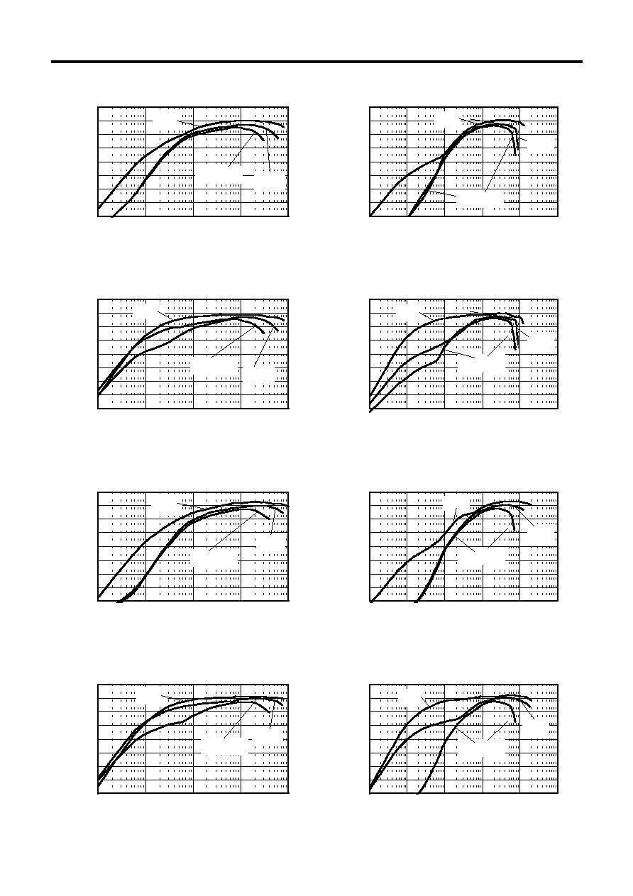
PWM Control & PWM/PFM Control High-Frequency Step-Up Switching Regulator-Controllers
Rev.2.1
_
60
S-8340/8341 Series
Seiko Instruments Inc.
37
(17) S-8340C33AFT
(18) S-8340C33AFT
20
30
40
50
60
70
80
90
100
I
OUT
(mA)
(
%)
V
IN
=1.2 V
3.0 V
1.8 V
(CDRH6D28/10
µH, FDN335N)
0.1
1
10
100
1000
20
30
40
50
60
70
80
90
100
(
%)
V
IN
=1.5 V
3.0 V
1.8 V
I
OUT
(mA)
(CDRH124/10
µH, FTS2001)
0.1
1
10
100
1000
10000
(19) S-8341C33AFT
(20) S-8341C33AFT
20
30
40
50
60
70
80
90
100
0.1
1
10
100
1000
I
OUT
(mA)
(
%)
V
IN
=1.2 V
3.0 V
1.8 V
(CDRH6D28/10
µH, FDN335N)
20
30
40
50
60
70
80
90
100
0.1
1
10
100
1000
10000
(
%)
V
IN
=1.5 V
3.0 V
1.8 V
I
OUT
(mA)
(CDRH124/10
µH, FTS2001)
(21) S-8340C50AFT
(22) S-8340C50AFT
20
30
40
50
60
70
80
90
100
I
OUT
(mA)
(
%)
V
IN
=1.8 V
3.0 V
4.5 V
(CDRH6D28/10
µH, FDN335N)
0.1
1
10
100
1000
20
30
40
50
60
70
80
90
100
(
%)
V
IN
=1.8 V
4.5 V
3.0 V
I
OUT
(mA)
(CDRH124/10
µH, FTS2001)
0.1
1
10
100
1000
10000
(23) S-8341C50AFT
(24) S-8341C50AFT
20
30
40
50
60
70
80
90
100
0.1
1
10
100
1000
I
OUT
(mA)
(
%)
V
IN
=1.8 V
3.0 V
4.5 V
(CDRH6D28/10
µH, FDN335N)
20
30
40
50
60
70
80
90
100
(
%)
V
IN
=1.8 V
4.5 V
3.0 V
I
OUT
(mA)
(CDRH124/10
µH, FTS2001)
0.1
1
10
100
1000
10000
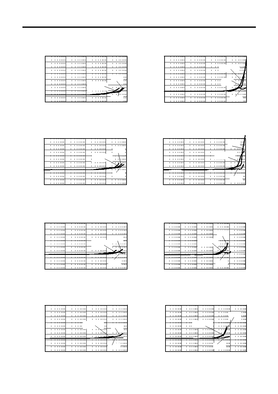
PWM Control & PWM/PFM Control High-Frequency Step-Up Switching Regulator-Controllers
S-8340/8341 Series
Rev.2.1
_60
Seiko Instruments Inc.
38
2. Output voltage V
OUT
--Output current I
OUT
Characteristics
(1) S-8340A25AFT
(2) S-8340A25AFT
2.46
2.48
2.50
2.52
2.54
2.56
2.58
2.60
2.62
0.1
1
10
100
1000
V
OUT
(V)
V
IN
=1.2 V
1.8 V
1.5 V
I
OUT
(mA)
(CDRH5D18/4.1
µH, NDS335N)
2.46
2.48
2.50
2.52
2.54
2.56
2.58
2.60
2.62
0.1
1
10
100
1000
V
OUT
(V)
V
IN
=1.5 V
2.4 V
1.8 V
I
OUT
(mA)
(CDRH124/10
µH, FTS2001)
(3) S-8341A25AFT
(4) S-8341A25AFT
2.46
2.48
2.50
2.52
2.54
2.56
2.58
2.60
2.62
0.1
1
10
100
1000
V
OUT
(V)
V
IN
=1.2 V
1.8 V
1.5 V
I
OUT
(mA)
(CDRH5D18/4.1
µH, NDS335N)
2.46
2.48
2.50
2.52
2.54
2.56
2.58
2.60
2.62
0.1
1
10
100
1000
V
OUT
(V)
V
IN
=1.5 V
2.4 V
1.8 V
I
OUT
(mA)
(CDRH124/10
µH, FTS2001)
(5) S-8340A33AFT
(6) S-8340A33AFT
3.20
3.25
3.30
3.35
3.40
3.45
3.50
3.55
3.60
0.1
1
10
100
1000
V
OUT
(V)
V
IN
=1.2 V
3.0 V
1.8 V
I
OUT
(mA)
(CDRH5D18/4.1
µH, NDS335N)
3.20
3.25
3.30
3.35
3.40
3.45
3.50
3.55
3.60
0.1
1
10
100
1000
10000
V
OUT
(V)
V
IN
=1.5 V
3.0 V
1.8 V
I
OUT
(mA)
(CDRH124/10
µH, FTS2001)
(7) S-8341A33AFT
(8) S-8341A33AFT
3.20
3.25
3.30
3.35
3.40
3.45
3.50
3.55
3.60
0.1
1
10
100
1000
V
OUT
(V)
V
IN
=1.2 V
3.0 V
1.8 V
I
OUT
(mA)
(CDRH5D18/4.1
µH, NDS335N)
3.20
3.25
3.30
3.35
3.40
3.45
3.50
3.55
3.60
0.1
1
10
100
1000
10000
V
OUT
(V)
V
IN
=1.5 V
3.0 V
1.8 V
I
OUT
(mA)
(CDRH124/10
µH, FTS2001)
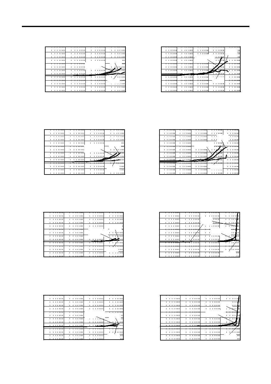
PWM Control & PWM/PFM Control High-Frequency Step-Up Switching Regulator-Controllers
Rev.2.1
_
60
S-8340/8341 Series
Seiko Instruments Inc.
39
(9) S-8340A50AFT
(10) S-8340A50AFT
4.90
4.95
5.00
5.05
5.10
5.15
5.20
5.25
5.30
0.1
1
10
100
1000
V
OUT
(V)
V
IN
=1.8 V
4.5 V
3.0 V
I
OUT
(mA)
(CDRH5D18/4.1
µH, NDS335N)
4.90
4.95
5.00
5.05
5.10
5.15
5.20
5.25
5.30
0.1
1
10
100
1000
10000
V
OUT
(V)
V
IN
=1.8 V
4.5 V
3.0 V
I
OUT
(mA)
(CDRH124/10
µH, FTS2001)
(11) S-8341A50AFT
(12) S-8341A50AFT
4.90
4.95
5.00
5.05
5.10
5.15
5.20
5.25
5.30
0.1
1
10
100
1000
V
OUT
(V)
V
IN
=1.8
4.5 V
3.0 V
I
OUT
(mA)
(CDRH5D18/4.1
µH, NDS335N)
4.90
4.95
5.00
5.05
5.10
5.15
5.20
5.25
5.30
0.1
1
10
100
1000
10000
V
OUT
(V)
V
IN
=1.8 V
4.5 V
3.0 V
I
OUT
(mA)
(CDRH124/10
µH, FTS2001)
(13) S-8340C25AFT
(14) S-8340C25AFT
2.46
2.48
2.50
2.52
2.54
2.56
2.58
2.60
2.62
0.1
1
10
100
1000
V
OUT
(V)
V
IN
=1.2 V
1.8 V
1.5 V
I
OUT
(mA)
(CDRH6D28/10
µH, FDN335N)
2.46
2.48
2.50
2.52
2.54
2.56
2.58
2.60
2.62
0.1
1
10
100
1000
V
OUT
(V)
V
IN
=1.5 V
2.4 V
1.8 V
I
OUT
(mA)
(CDRH124/10
µH, FTS2001)
(15) S-8341C25AFT
(16) S-8341C25AFT
2.46
2.48
2.50
2.52
2.54
2.56
2.58
2.60
2.62
0.1
1
10
100
1000
V
OUT
(V)
V
IN
=1.2 V
1.8 V
1.5 V
I
OUT
(mA)
(CDRH6D28/10
µH, FDN335N)
2.46
2.48
2.50
2.52
2.54
2.56
2.58
2.60
2.62
0.1
1
10
100
1000
V
OUT
(V)
V
IN
=1.5 V
2.4 V
1.8 V
I
OUT
(mA)
(CDRH124/10
µH, FTS2001)
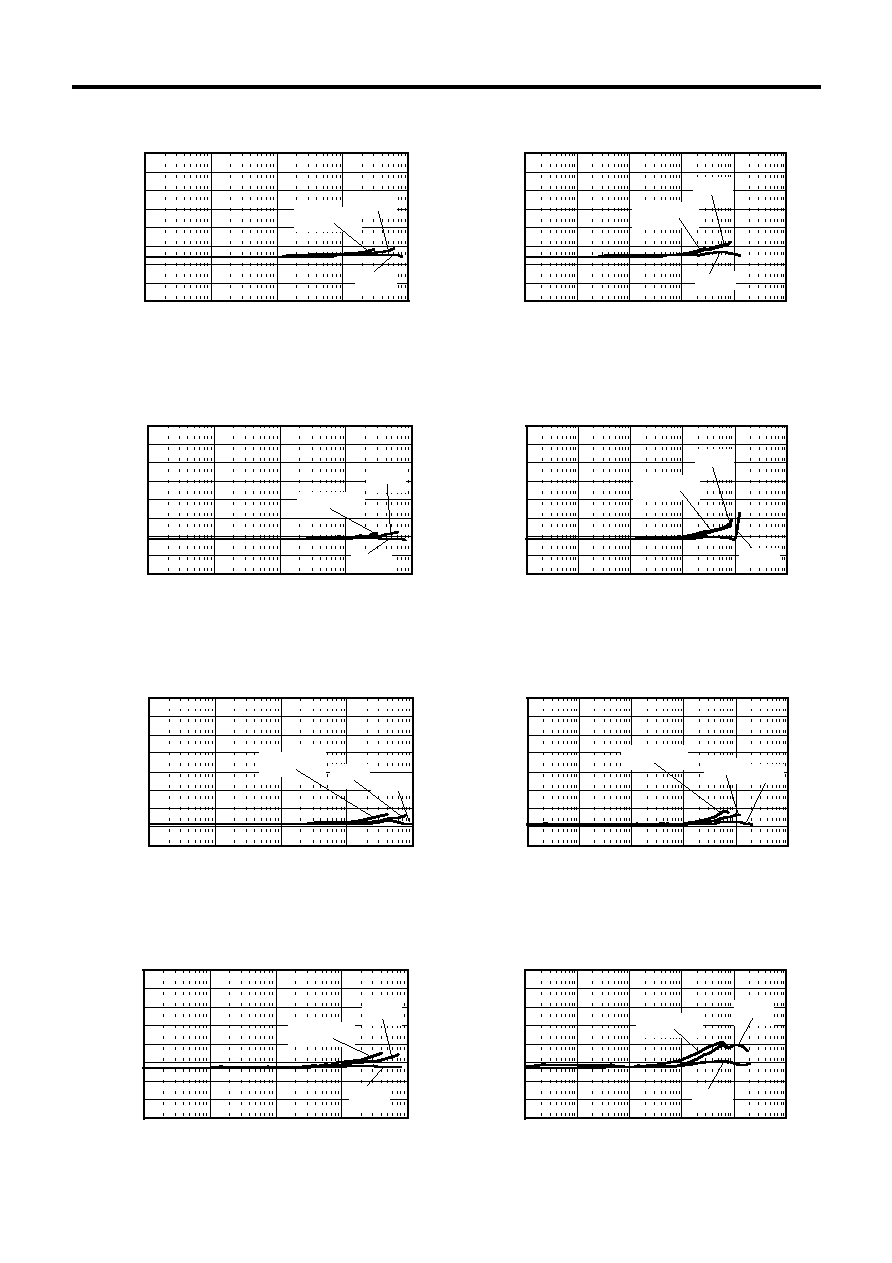
PWM Control & PWM/PFM Control High-Frequency Step-Up Switching Regulator-Controllers
S-8340/8341 Series
Rev.2.1
_60
Seiko Instruments Inc.
40
(17) S-8340C33AFT
(18) S-8340C33AFT
3.20
3.25
3.30
3.35
3.40
3.45
3.50
3.55
3.60
0.1
1
10
100
1000
V
OUT
(V)
V
IN
=1.2 V
3.0 V
1.8 V
I
OUT
(mA)
(CDRH6D28/10
µH, FDN335N)
3.20
3.25
3.30
3.35
3.40
3.45
3.50
3.55
3.60
0.1
1
10
100
1000
10000
V
OUT
(V)
V
IN
=1.5 V
3.0 V
1.8 V
I
OUT
(mA)
(CDRH124/10
µH, FTS2001)
(19) S-8341C33AFT
(20) S-8341C33AFT
3.20
3.25
3.30
3.35
3.40
3.45
3.50
3.55
3.60
0.1
1
10
100
1000
V
OUT
(V)
V
IN
=1.2 V
3.0 V
1.8 V
I
OUT
(mA)
(CDRH6D28/10
µH, FDN335N)
3.20
3.25
3.30
3.35
3.40
3.45
3.50
3.55
3.60
0.1
1
10
100
1000
10000
V
OUT
(V)
V
IN
=1.5 V
3.0 V
1.8 V
I
OUT
(mA)
(CDRH124/10
µH, FTS2001)
(21) S-8340C50AFT
(22) S-8340C50AFT
4.90
4.95
5.00
5.05
5.10
5.15
5.20
5.25
5.30
0.1
1
10
100
1000
V
OUT
(V)
V
IN
=1.8 V
4.5 V
3.0 V
I
OUT
(mA)
(CDRH6D28/10
µH, FDN335N)
4.90
4.95
5.00
5.05
5.10
5.15
5.20
5.25
5.30
0.1
1
10
100
1000
10000
V
OUT
(V)
V
IN
=1.8 V
4.5 V
3.0 V
I
OUT
(mA)
(CDRH124/10
µH, FTS2001)
(23) S-8341C50AFT
(24) S-8341C50AFT
4.90
4.95
5.00
5.05
5.10
5.15
5.20
5.25
5.30
0.1
1
10
100
1000
V
OUT
(V)
V
IN
=1.8 V
4.5 V
3.0 V
I
OUT
(mA)
(CDRH6D28/10
µH, FDN335N)
4.90
4.95
5.00
5.05
5.10
5.15
5.20
5.25
5.30
0.1
1
10
100
1000
10000
V
OUT
(V)
V
IN
=1.8 V
4.5 V
3.0 V
I
OUT
(mA)
(CDRH124/10
µH, FTS2001)
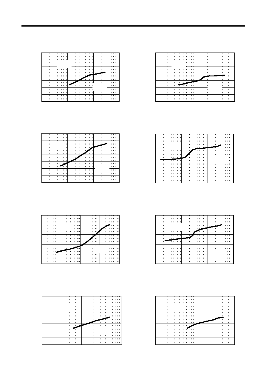
PWM Control & PWM/PFM Control High-Frequency Step-Up Switching Regulator-Controllers
Rev.2.1
_
60
S-8340/8341 Series
Seiko Instruments Inc.
41
3. PFM/PWM-switched input voltage V
IN
- output current V
OUT
characteristics (Output current increase)
(25) S-8341A25AFT
(26) S-8341A25AFT
V
IN
(V)
0.0
0.5
1.0
1.5
2.0
2.5
3.0
3.5
1
10
100
1000
I
OUT
(mA)
(CDRH5D18/4.1
µH, NDS335N)
PFM
PWM
V
IN
(V)
0.0
0.5
1.0
1.5
2.0
2.5
3.0
3.5
1
10
100
I
OUT
(mA)
(CDRH124/10
µH, FTS2001)
PFM
PWM
(27) S-8341A33AFT
(28) S-8341A33AFT
V
IN
(V)
0.0
0.5
1.0
1.5
2.0
2.5
3.0
3.5
1
10
100
1000
I
OUT
(mA)
(CDRH5D18/4.1
µH, NDS335N)
PFM
PWM
V
IN
(V)
0.0
0.5
1.0
1.5
2.0
2.5
3.0
3.5
1
10
100
1000
I
OUT
(mA)
(CDRH124/10
µH, FTS2001)
PFM
PWM
(29) S-8341A50AFT
(30) S-8341A50AFT
V
IN
(V)
0.0
1.0
2.0
3.0
4.0
5.0
0.1
1
10
100
1000
I
OUT
(mA)
(CDRH5D18/4.1
µH, NDS335N)
PFM
PWM
V
IN
(V)
0.0
1.0
2.0
3.0
4.0
5.0
1
10
100
1000
I
OUT
(mA)
(CDRH124/10
µH, FTS2001)
PFM
PWM
(31) S-8341C25AFT
(32) S-8341C25AFT
V
IN
(V)
0.0
0.5
1.0
1.5
2.0
2.5
3.0
3.5
1
10
100
I
OUT
(mA)
(CDRH6D28/10
µH, FDN335N)
PFM
PWM
V
IN
(V)
0.0
0.5
1.0
1.5
2.0
2.5
3.0
3.5
1
10
100
I
OUT
(mA)
(CDRH124/10
µH, FTS2001)
PFM
PWM
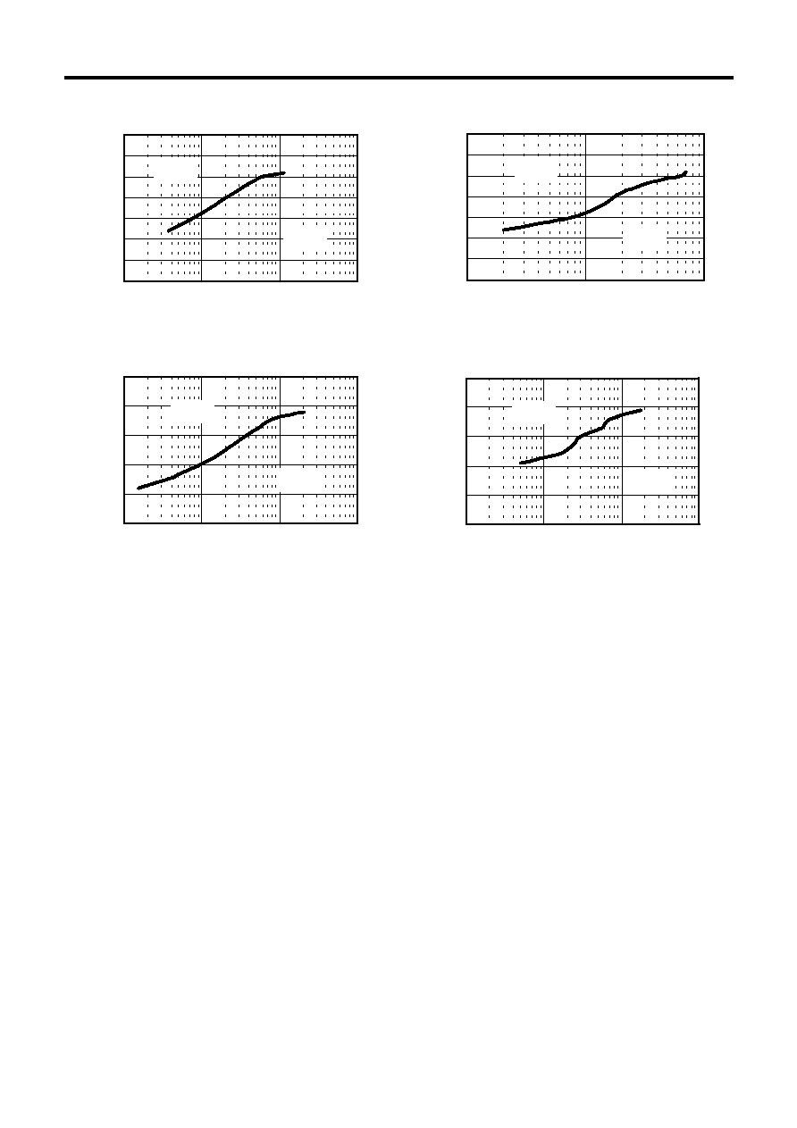
PWM Control & PWM/PFM Control High-Frequency Step-Up Switching Regulator-Controllers
S-8340/8341 Series
Rev.2.1
_60
Seiko Instruments Inc.
42
(33) S-8341C33AFT
(34) S-8341C33AFT
V
IN
(V)
0.0
0.5
1.0
1.5
2.0
2.5
3.0
3.5
1
10
100
1000
I
OUT
(mA)
(CDRH6D28/10
µH, FDN335N)
PFM
PWM
V
IN
(V)
0.0
0.5
1.0
1.5
2.0
2.5
3.0
3.5
1
10
100
I
OUT
(mA)
(CDRH124/10
µH, FTS2001)
PFM
PWM
(35) S-8341C50AFT
(36) S-8341C50AFT
V
IN
(V)
0.0
1.0
2.0
3.0
4.0
5.0
1
10
100
1000
I
OUT
(mA)
(CDRH6D28/10
µH, FDN335N)
PFM
PWM
V
IN
(V)
0.0
1.0
2.0
3.0
4.0
5.0
1
10
100
1000
I
OUT
(mA)
(CDRH124/10
µH, FTS2001)
PFM
PWM

PWM Control & PWM/PFM Control High-Frequency Step-Up Switching Regulator-Controllers
Rev.2.1
_
60
S-8340/8341 Series
Seiko Instruments Inc.
43
4. Ripple--Output current I
OUT
Characteristics
(37) S-8340A25AFT
Ripple
(mV)
0
50
100
150
200
250
300
1
10
100
1000
I
OUT
(mA)
(CDRH5D18/4.1
µH, NDS335N,47 µF)
V
IN
=1.2 V
1.5 V
1.8 V
Ripple
(mV)
0
50
100
150
200
250
300
1
10
100
1000
I
OUT
(mA)
(CDRH5D18/4.1
µH,NDS335N,47 µF◊2)
V
IN
=1.2 V
1.5 V
1.8 V
(38) S-8340A25AFT
Ripple
(mV)
0
100
200
300
400
500
600
10
100
1000
10000
I
OUT
(mA)
(CDRH124/10
µH, FTS2001,47 µF◊2)
1.8 V
V
IN
=1.5 V
2.4 V
Ripple
(mV)
0
100
200
300
400
500
600
10
100
1000
10000
I
OUT
(mA)
(CDRH124/10
µH, FTS2001,100 µF◊2)
2.4 V
V
IN
=1.5 V
1.8 V
(39) S-8341A25AFT
Ripple
(mV)
0
50
100
150
200
250
300
1
10
100
1000
I
OUT
(mA)
(CDRH5D18/4.1
µH, NDS335N,47 µF)
1.8 V
1.5 V
V
IN
=1.2 V
Ripple
(mV)
0
50
100
150
200
250
300
1
10
100
1000
I
OUT
(mA)
(CDRH5D18/4.1
µH, NDS335N,47 µF◊2)
1.8 V
1.5 V
V
IN
=1.2 V
(40) S-8341A25AFT
Ripple
(mV)
0
100
200
300
400
500
600
10
100
1000
10000
I
OUT
(mA)
(CDRH124/10
µH, FTS2001,47 µF◊2)
1.8 V
V
IN
=1.5 V
2.4 V
Ripple
(mV)
0
100
200
300
400
500
600
10
100
1000
10000
I
OUT
(mA)
(CDRH124/10
µH, FTS2001,100 µF◊2)
1.8 V
V
IN
=1.5 V
2.4 V
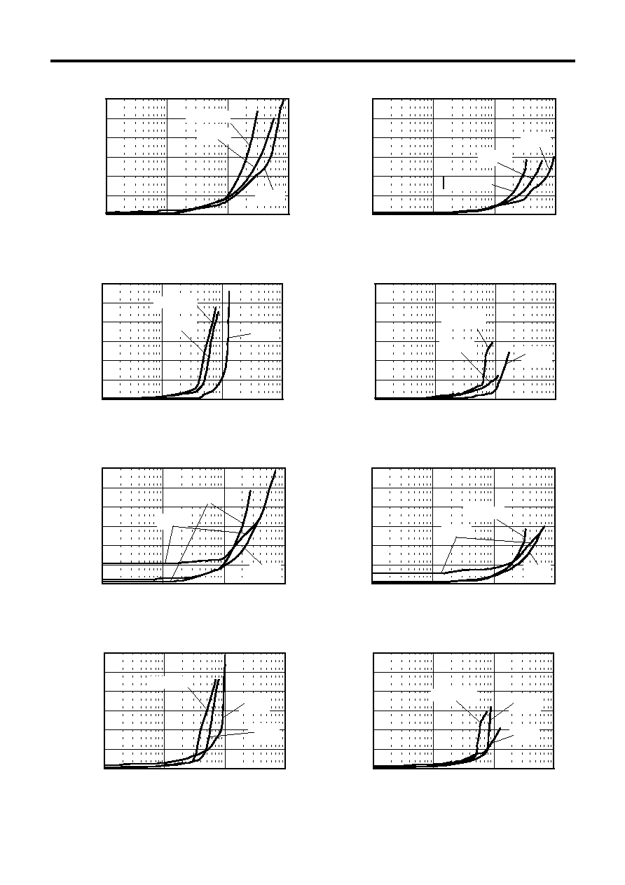
PWM Control & PWM/PFM Control High-Frequency Step-Up Switching Regulator-Controllers
S-8340/8341 Series
Rev.2.1
_60
Seiko Instruments Inc.
44
(41) S-8340A33AFT
Ripple
(mV)
0
50
100
150
200
250
300
1
10
100
1000
I
OUT
(mA)
(CDRH5D18/4.1
µH, NDS335N,47 µF)
1.8 V
V
IN
=1.2 V
3.0 V
Ripple
(mV)
0
50
100
150
200
250
300
1
10
100
1000
I
OUT
(mA)
(CDRH5D18/4.1
µH, NDS335N,47 µF◊2)
1.8 V
V
IN
=1.2 V
3.0 V
(42) S-8340A33AFT
Ripple
(mV)
0
100
200
300
400
500
600
10
100
1000
10000
I
OUT
(mA)
(CDRH124/10
µH, FTS2001,47 µF◊2)
1.8 V
V
IN
=1.5 V
3.0 V
Ripple
(mV)
0
100
200
300
400
500
600
10
100
1000
10000
I
OUT
(mA)
(CDRH124/10
µH, FTS2001,100 µF◊2)
1.8 V
V
IN
=1.5 V
3.0 V
(43) S-8341A33AFT
Ripple
(mV)
0
50
100
150
200
250
300
1
10
100
1000
I
OUT
(mA)
(CDRH5D18/4.1
µH, NDS335N,47 µF)
1.8 V
V
IN
=1.2 V
3.0 V
Ripple
(mV)
0
50
100
150
200
250
300
1
10
100
1000
I
OUT
(mA)
(CDRH5D18/4.1
µH,NDS335N,47 µF◊2)
1.8 V
V
IN
=1.2 V
3.0 V
(44) S-8341A33AFT
Ripple
(mV)
0
100
200
300
400
500
600
10
100
1000
10000
I
OUT
(mA)
(CDRH124/10
µH, FTS2001,47 µF◊2)
1.8 V
V
IN
=1.5 V
3.0 V
Ripple
(mV)
0
100
200
300
400
500
600
10
100
1000
10000
I
OUT
(mA)
(CDRH124/10
µH,FTS2001,100 µF◊2)
1.8 V
V
IN
=1.5 V
3.0 V

PWM Control & PWM/PFM Control High-Frequency Step-Up Switching Regulator-Controllers
Rev.2.1
_
60
S-8340/8341 Series
Seiko Instruments Inc.
45
(45) S-8340A50AFT
Ripple
(mV)
0
50
100
150
200
250
300
1
10
100
1000
I
OUT
(mA)
(CDRH5D18/4.1
µH, NDS335N,47 µF)
V
IN
=1.8 V
4.5 V
3.0 V
Ripple
(mV)
0
50
100
150
200
250
300
1
10
100
1000
I
OUT
(mA)
(CDRH5D18/4.1
µH,NDS335N,47 µF◊2)
V
IN
=1.8 V
4.5 V
3.0 V
(46) S-8340A50AFT
Ripple
(mV)
0
50
100
150
200
250
300
350
10
100
1000
10000
I
OUT
(mA)
(CDRH124/10
µH, FTS2001,47 µF◊2)
V
IN
=1.8 V
4.5 V
3.0 V
Ripple
(mV)
0
50
100
150
200
250
300
350
10
100
1000
10000
I
OUT
(mA)
(CDRH124/10
µH,FTS2001,100 µF◊2)
V
IN
=1.8 V
4.5 V
3.0 V
(47) S-8341A50AFT
Ripple
(mV)
0
50
100
150
200
250
300
350
1
10
100
1000
I
OUT
(mA)
(CDRH5D18/4.1
µH, NDS335N,47 µF)
V
IN
=1.8 V
4.5 V
3.0 V
Ripple
(mV)
0
50
100
150
200
250
300
350
1
10
100
1000
I
OUT
(mA)
(CDRH5D18/4.1
µH, NDS335N,47 µF◊2)
V
IN
=1.8 V
4.5 V
3.0 V
(48) S-8341A50AFT
Ripple
(mV)
0
100
200
300
400
500
600
10
100
1000
10000
I
OUT
(mA)
(CDRH124/10
µH, FTS2001,47 µF◊2)
V
IN
=1.8 V
4.5 V
3.0 V
Ripple
(mV)
0
100
200
300
400
500
600
10
100
1000
10000
I
OUT
(mA)
(CDRH124/10
µH, FTS2001,100 µF◊2)
V
IN
=1.8 V
4.5 V
3.0 V
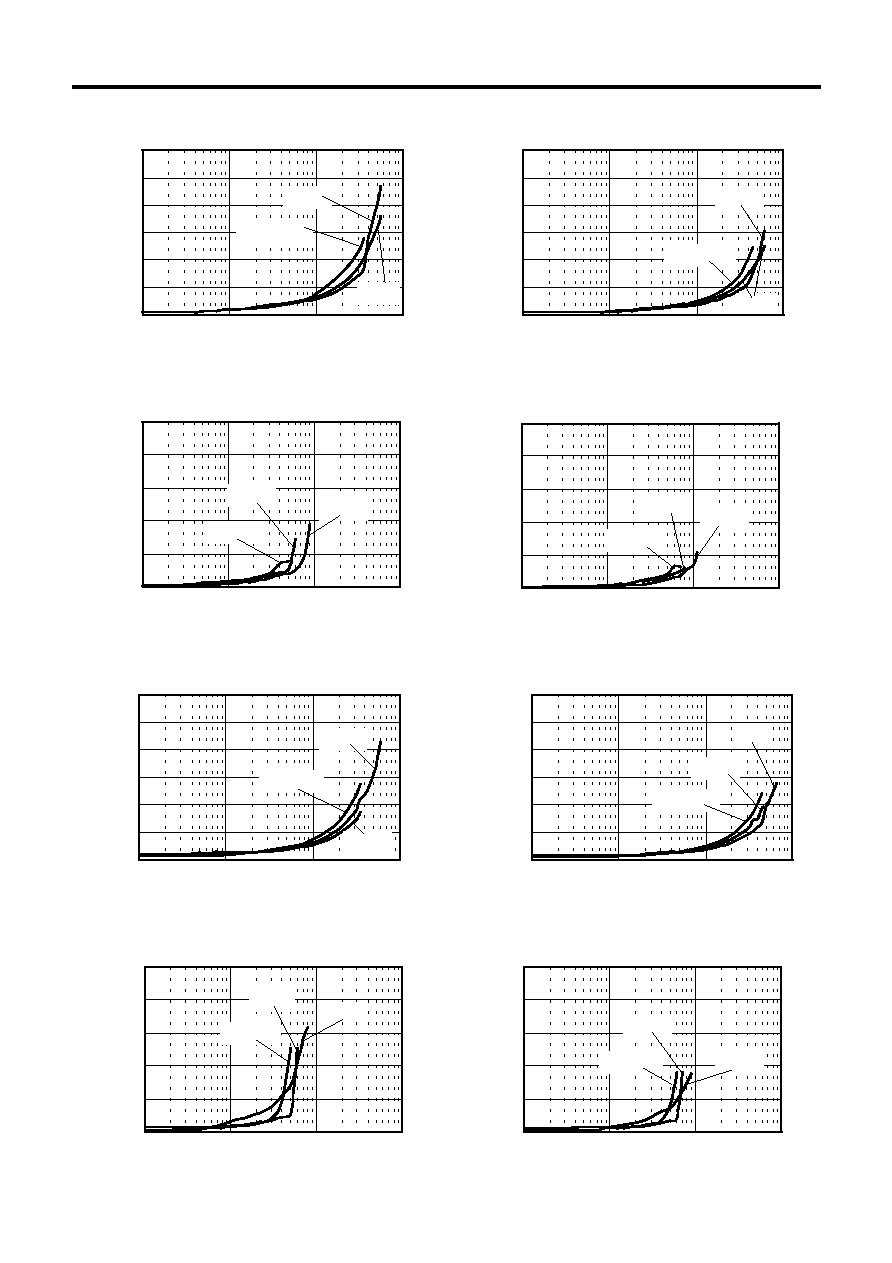
PWM Control & PWM/PFM Control High-Frequency Step-Up Switching Regulator-Controllers
S-8340/8341 Series
Rev.2.1
_60
Seiko Instruments Inc.
46
(49) S-8340C25AFT
Ripple
(mV)
0
50
100
150
200
250
300
1
10
100
1000
I
OUT
(mA)
(CDRH6D28/10
µH, FDN335N, 47 µF)
V
IN
=1.2 V
1.5 V
1.8 V
Ripple
(mV)
0
50
100
150
200
250
300
1
10
100
1000
I
OUT
(mA)
(CDRH6D28/10
µH, FDN335N,100 µF)
V
IN
=1.2 V
1.5 V
1.8 V
(50) S-8340C25AFT
Ripple
(mV)
0
100
200
300
400
500
10
100
1000
10000
I
OUT
(mA)
(CDRH124/10
µH, FTS2001, 47 µF◊2)
1.8 V
V
IN
=1.5 V
2.4 V
Ripple
(mV)
0
100
200
300
400
500
10
100
1000
10000
I
OUT
(mA)
(CDRH124/10
µH, FTS2001, 100 µF◊2)
2.4 V
V
IN
=1.5 V
1.8 V
(51) S-8341C25AFT
Ripple
(mV)
0
50
100
150
200
250
300
1
10
100
1000
I
OUT
(mA)
(CDRH6D28/10
µH, FDN335N,47 µF)
1.8 V
1.5 V
V
IN
=1.2 V
Ripple
(mV)
0
50
100
150
200
250
300
1
10
100
1000
I
OUT
(mA)
(CDRH6D28/10
µH, FDN335N,100 µF)
1.8 V
1.5 V
V
IN
=1.2 V
(52) S-8341C25AFT
Ripple
(mV)
0
100
200
300
400
500
10
100
1000
10000
I
OUT
(mA)
(CDRH124/10
µH, FTS2001,47
1.8 V
V
IN
=1.5 V
2.4 V
Ripple
(mV)
0
100
200
300
400
500
10
100
1000
10000
I
OUT
(mA)
(CDRH124/10
µH, FTS2001,100 µF◊2)
1.8 V
V
IN
=1.5 V
2.4 V
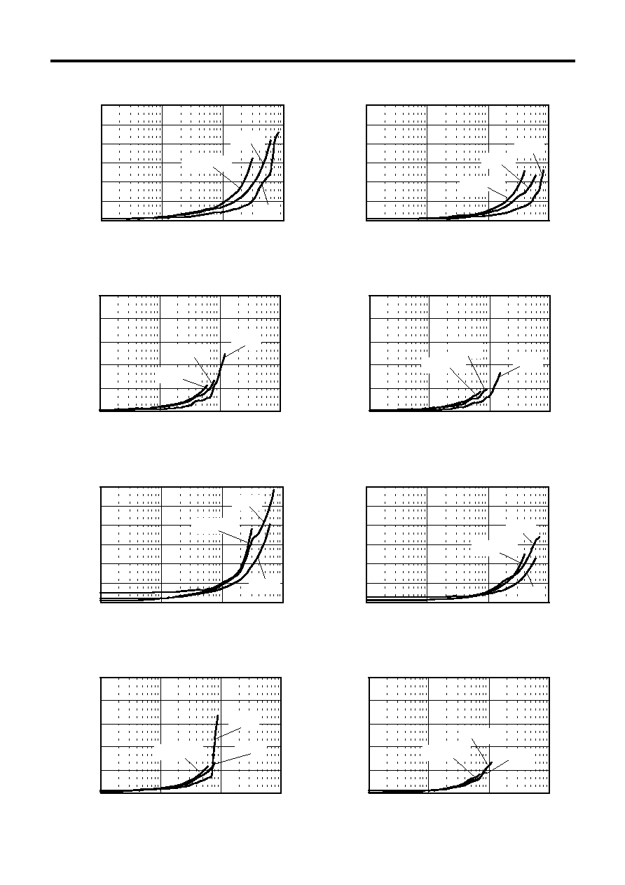
PWM Control & PWM/PFM Control High-Frequency Step-Up Switching Regulator-Controllers
Rev.2.1
_
60
S-8340/8341 Series
Seiko Instruments Inc.
47
(53) S-8340C33AFT
Ripple
(mV)
0
50
100
150
200
250
300
1
10
100
1000
I
OUT
(mA)
(CDRH6D28/10
µH, FDN335N,47 µF)
1.8 V
V
IN
=1.2 V
3.0 V
Ripple
(mV)
0
50
100
150
200
250
300
1
10
100
1000
I
OUT
(mA)
(CDRH6D28/10
µH, FDN335N,100 µF)
1.8 V
V
IN
=1.2 V
3.0 V
(54) S-8340C33AFT
Ripple
(mV)
0
100
200
300
400
500
10
100
1000
10000
I
OUT
(mA)
(CDRH124/10
µH, FTS2001,47 µF◊2)
1.8 V
V
IN
=1.5 V
3.0 V
Ripple
(mV)
0
100
200
300
400
500
10
100
1000
10000
I
OUT
(mA)
(CDRH124/10
µH, FTS2001,100 µF◊2)
1.8 V
V
IN
=1.5 V
3.0 V
(55) S-8341C33AFT
Ripple
(mV)
0
50
100
150
200
250
300
1
10
100
1000
I
OUT
(mA)
(CDRH6D28/10
µH, FDN335N,47 µF)
1.8 V
V
IN
=1.2 V
3.0 V
Ripple
(mV)
0
50
100
150
200
250
300
1
10
100
1000
I
OUT
(mA)
(CDRH6D28/10
µH, FDN335N,100 µF)
1.8 V
V
IN
=1.2 V
3.0 V
(56) S-8341C33AFT
Ripple
(mV)
0
100
200
300
400
500
10
100
1000
10000
I
OUT
(mA)
(CDRH124/10
µH, FTS2001,47 µF◊2)
1.8 V
V
IN
=1.5
3.0 V
Ripple
(mV)
0
100
200
300
400
500
10
100
1000
10000
I
OUT
(mA)
(CDRH124/10
µH, FTS2001,100 µF◊2)
1.8 V
V
IN
=1.5 V
3.0 V
PWM Control & PWM/PFM Control High-Frequency Step-Up Switching Regulator-Controllers
S-8340/8341 Series
Rev.2.1
_60
Seiko Instruments Inc.
48
(57) S-8340C50AFT
Ripple
(mV)
0
50
100
150
200
250
300
1
10
100
1000
I
OUT
(mA)
(CDRH6D28/10
µH, FDN335N,47 µF)
V
IN
=1.8 V
4.5 V
3.0 V
Ripple
(mV)
0
50
100
150
200
250
300
1
10
100
1000
I
OUT
(mA)
(CDRH6D28/10
µH, FDN335N,100 µF)
V
IN
=1.8 V
4.5 V
3.0 V
(58) S-8340C50AFT
Ripple
(mV)
0
100
200
300
400
500
10
100
1000
10000
I
OUT
(mA)
(CDRH124/10
µH, FTS2001,47 µF◊2)
V
IN
=1.8 V
4.5 V
3.0 V
Ripple
(mV)
0
100
200
300
400
500
10
100
1000
10000
I
OUT
(mA)
(CDRH124/10
µH, FTS2001,100 µF◊2)
V
IN
=1.8 V
4.5 V
3.0 V
(59) S-8341C50AFT
Ripple
(mV)
0
50
100
150
200
250
300
1
10
100
1000
I
OUT
(mA)
(CDRH6D28/10
µH, FDN335N,47 µF)
V
IN
=1.8 V
4.5 V
3.0 V
Ripple
(mV)
0
50
100
150
200
250
300
1
10
100
1000
I
OUT
(mA)
(CDRH6D28/10
µH, FDN335N,100 µF)
V
IN
=1.8 V
4.5 V
3.0 V
(60) S-8341C50AFT
Ripple
(mV)
0
100
200
300
400
500
10
100
1000
10000
I
OUT
(mA)
(CDRH124/10
µH, FTS2001,47 µF◊2)
V
IN
=1.8 V
4.5 V
3.0 V
Ripple
(mV)
0
100
200
300
400
500
10
100
1000
10000
I
OUT
(mA)
(CDRH124/10
µH, FTS2001,100 µF◊2)
V
IN
=1.8 V
4.5 V
3.0 V
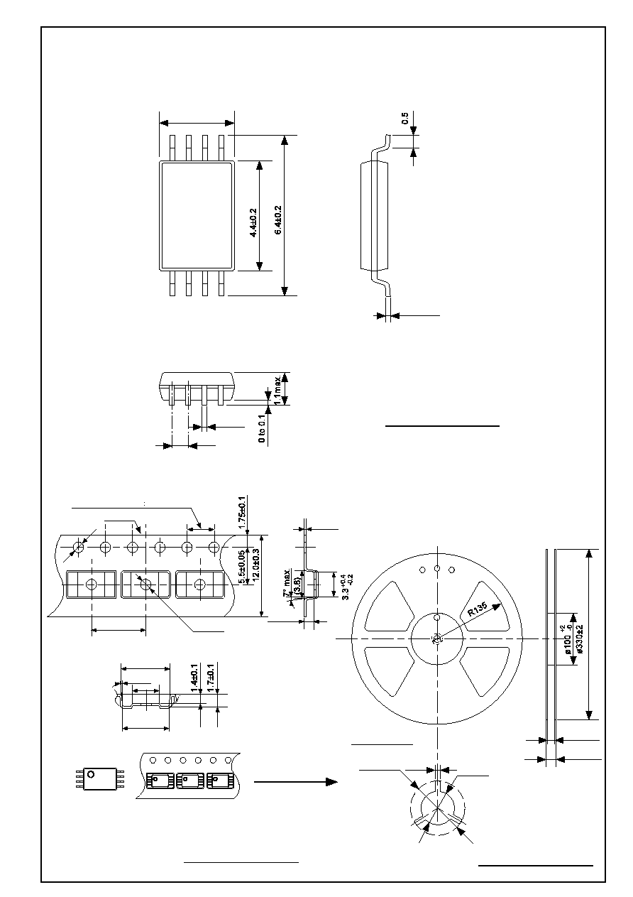
n
8-Pin TSSOP
FT008-A 020808
Unit:mm
lDimensions
lTaping Specifications
lReel Specifications
0.17±0.05
3.00
1
4
5
8
+0.3
-0.2
0.65
0.2±0.1
No. : FT008-A-P-SD-1.0
¯13±0.5
2±0.5
¯21±0.8
Winding core
1 reel holds 3000 ICs.
13.4±1.0
17.5±1.0
No. : FT008-A-R-SD-3.0
T2
1
4
5
8
Feed direction
1.55±0.05
4.0±0.1(50 pitches 200.0±0.3)
2.0±0.05
8.0±0.1
1.55
+0.1
-0
1.4±0.1
0.3±0.05
(6.9)
4.0
+0.4
-0.2
6.6
7∞ max.
No. : FT008-A-C-SD-3.0

∑
The information described herein is subject to change without notice.
∑
Seiko Instruments Inc. is not responsible for any problems caused by circuits or diagrams described herein
whose related industrial properties, patents, or other rights belong to third parties. The application circuit
examples explain typical applications of the products, and do not guarantee the success of any specific
mass-production design.
∑
When the products described herein are regulated products subject to the Wassenaar Arrangement or other
agreements, they may not be exported without authorization from the appropriate governmental authority.
∑
Use of the information described herein for other purposes and/or reproduction or copying without the
express permission of Seiko Instruments Inc. is strictly prohibited.
∑
The products described herein cannot be used as part of any device or equipment affecting the human
body, such as exercise equipment, medical equipment, security systems, gas equipment, or any apparatus
installed in airplanes and other vehicles, without prior written permission of Seiko Instruments Inc.
∑
Although Seiko Instruments Inc. exerts the greatest possible effort to ensure high quality and reliability, the
failure or malfunction of semiconductor products may occur. The user of these products should therefore
give thorough consideration to safety design, including redundancy, fire-prevention measures, and
malfunction prevention, to prevent any accidents, fires, or community damage that may ensue.