
Rev.1.0
_10
SMALL PACKAGE PFM CONTROL STEP-UP SWITCHING REGULATOR
S-8351/52 Series
Seiko Instruments Inc.
1
The S-8351/8352 Series is a CMOS PFM-control step-up
switching regulator that mainly consists of a reference voltage
source, an oscillator, and a comparator. The PFM controller
allows the duty ratio to be automatically switched according to
the load (light load: 50%, high output current: 75%), enabling
products with a low ripple over a wide range, high efficiency, and
high output current (product types A, B, and D). Products with a
fixed duty ratio of 75% are also available (product type C).
With the S-8351 Series, a step-up switching regulator can be
configured by using an external coil, capacitor, and diode. The
built-in MOS FET is turned off by a protection circuit when the
voltage at the CONT pin exceeds the limit to prevent it from
being damaged. This feature, along with the mini package and
low current consumption, makes the S-8351 Series ideal for
applications such as the power supply unit of portable
equipment.
The S-8352 Series, which features an external transistor, is
suitable for applications requiring a high output current.
Features
∑ Low voltage operation: Startup at 0.9 V min. (I
OUT
= 1 mA) guaranteed
∑ Low input current:
During maximum operation: 23.2
ĶA (V
OUT
= 3.3 V, typ.)
During shutdown: 0.5
ĶA (max.)
∑ Duty ratio:
50/75%, built-in auto-switching-type PFM controller (product types A, B, D)
75%, built-in fixed-type PFM controller (product type C)
∑ External parts:
Coil, capacitor, diode
∑ Output voltage:
Settable to between 2.0 to 6.5 V (product types A, B, C) or 1.5 to 6.5 V (product
type D) in 0.1 V steps, accuracy of
Ī2.4%
∑ Shutdown function (product type A)
∑ V
DD
/V
OUT
separate type (product type D)
∑ External transistor type available (S-8352 Series)
Packages
∑ SOT-23-3 (package drawing code: MP003-A)
∑ SOT-23-5 (package drawing code: MP005-A)
∑ SOT-89-3 (package drawing code: UP003-A)
Applications
∑ Power supply for portable equipment such as digital cameras, electronic notebooks, and PDAs
∑ Power supply for audio equipment such as portable CD/MD players
∑ Constant voltage power supply for cameras, video equipment, and communications equipment
∑ Power supply for microcomputers

SMALL PACKAGE PFM CONTROL STEP-UP SWITCHING REGULATOR
S-8351/52 Series
Rev.1.0
_10
Seiko Instruments Inc.
2
Applications
1. Function List
Product Name
Control System
(Duty Ratio (%))
Switching
Frequency (kHz)
Shutdown
Function
V
DD
/V
OUT
Separate Type
Power
MOS FET
Package
Application
S-8351AxxMC
PFM (50/75)
100
Yes
Built-in
SOT-23-5
Application requiring shutdown function
S-8351BxxMA
PFM (50/75)
100
Built-in
SOT-23-3
Application not requiring shutdown function
S-8351CxxMA
PFM (75)
100
Built-in
SOT-23-3
Application not requiring shutdown function
S-8351CxxUA
PFM (75)
100
Built-in
SOT-89-3
Application not requiring shutdown function
S-8351DxxMC
PFM (50/75)
100
Yes
Built-in
SOT-23-5
Application in which output voltage is
adjusted by external resistance
S-8352AxxMC
PFM (50/75)
100
Yes
External
SOT-23-5
Application requiring shutdown function
S-8352BxxMA
PFM (50/75)
100
External
SOT-23-3
Application not requiring shutdown function
S-8352CxxMA
PFM (75)
100
External
SOT-23-3
Application not requiring shutdown function
S-8352CxxUA
PFM (75)
100
External
SOT-89-3
Application not requiring shutdown function
S-8352DxxMC
PFM (50/75)
100
Yes
External
SOT-23-5
Application in which output voltage is
adjusted by external resistance
2.
Product Name
S-835 X X XX XX
- XXX - T2
Series name
1; Built-in power MOS FET
2; External power MOS FET
IC direction in tape specification
Product name
Package name
MA; SOT-23-3 (without shutdown function)
MC; SOT-23-5 (with shutdown function or V
DD
/V
OUT
separate type)
UA; SOT-89-3 (without shutdown function)
Output voltage ◊ 10 (15 for output voltage value 1.5)
Product type
A ; With shutdown function
B ; Automatic duty ratio switching type
C ; Duty ratio fixed type (75%)
D ; V
DD
/V
OUT
separate type

SMALL PACKAGE PFM CONTROL STEP-UP SWITCHING REGULATOR
Rev.1.0
_10
S-8351/52 Series
Seiko Instruments Inc.
3
3. Product Name List
Output Voltage
S-8351AxxMC
Series
S-8351BxxMA
Series
S-8351CxxMA
S-8351CxxUA
Series
S-8351DxxMC
Series
3.0
S-8351A30MC-J2P-T2 S-8351B30MA-J4P-T2
3.3
S-8351A33MC-J2S-T2
3.5
S-8351A35MC-J2U-T2
5.0
S-8351A50MC-J3J-T2
5.5
S-8351A55MC-J3O-T2
Output Voltage
S-8352AxxMC
Series
S-8352BxxMA
Series
S-8352CxxMA
S-8352CxxUA
Series
S-8352DxxMC
Series
2.0
S-8352D20MC-K8F-T2
3.0
S-8352A30MC-K2P-T2 S-8352B30MA-K4P-T2
5.0
S-8352A50MC-K3J-T2
Remark Please consult our sales staff if you require a product with an output voltage other than those specified
above.
SMALL PACKAGE PFM CONTROL STEP-UP SWITCHING REGULATOR
S-8351/52 Series
Rev.1.0
_10
Seiko Instruments Inc.
4
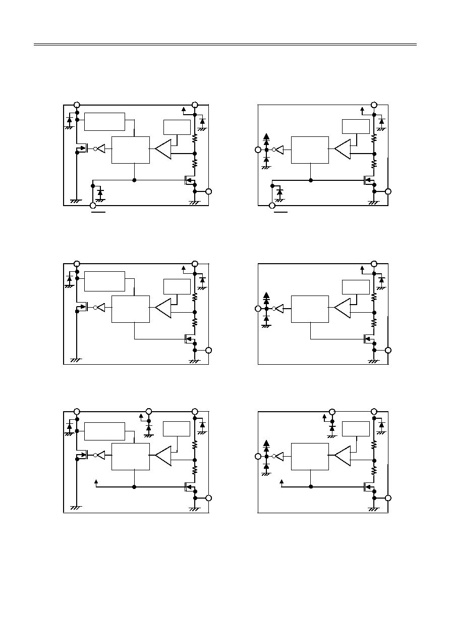
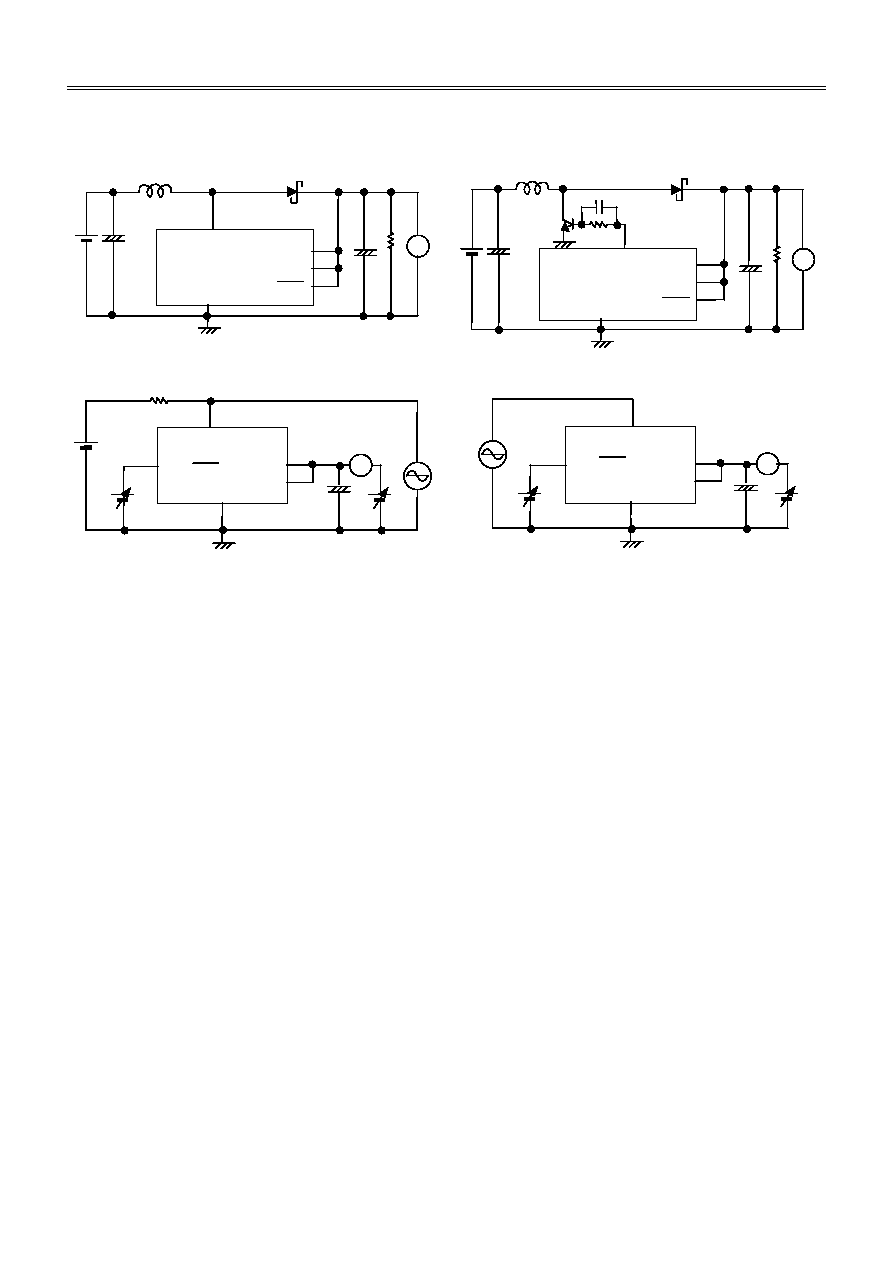
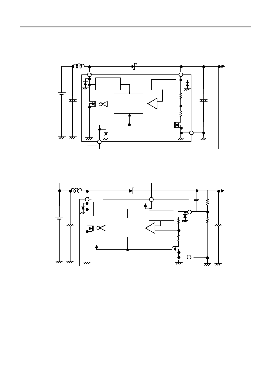
Block Diagrams
EXT
(1) S-8351 Series A type (with shutdown function)
VSS
IC internal power supply
IC internal
power supply
IC internal
power supply
IC internal
power supply
VOUT
CONT
Protection
circuit
PFM
controller
-
+
V
REF
ON/OFF
VSS
VOUT
PFM
controller
-
+
V
REF
EXT
VSS
VDD
VDD
VOUT
CONT
Protection
circuit
PFM
controller
-
+
V
REF
VSS
VOUT
PFM
controller
-
+
V
REF
(5) S-8351 Series D type (V
DD
/V
OUT
separate type)
EXT
(3) S-8351 Series B, C type (without shutdown function)
VSS
IC internal
power supply
IC internal
power supply
VOUT
CONT
Protection
circuit
PFM
controller
-
+
V
REF
VSS
VOUT
PFM
controller
-
+
V
REF
(2) S-8352 Series A type (with shutdown function)
(6) S-8352 Series D type (V
DD
/V
OUT
separate type)
(4) S-8352 Series B, C type (without shutdown function)
ON/OFF
Figure 1. Block Diagrams
SMALL PACKAGE PFM CONTROL STEP-UP SWITCHING REGULATOR
Rev.1.0
_10
S-8351/52 Series
Seiko Instruments Inc.
5
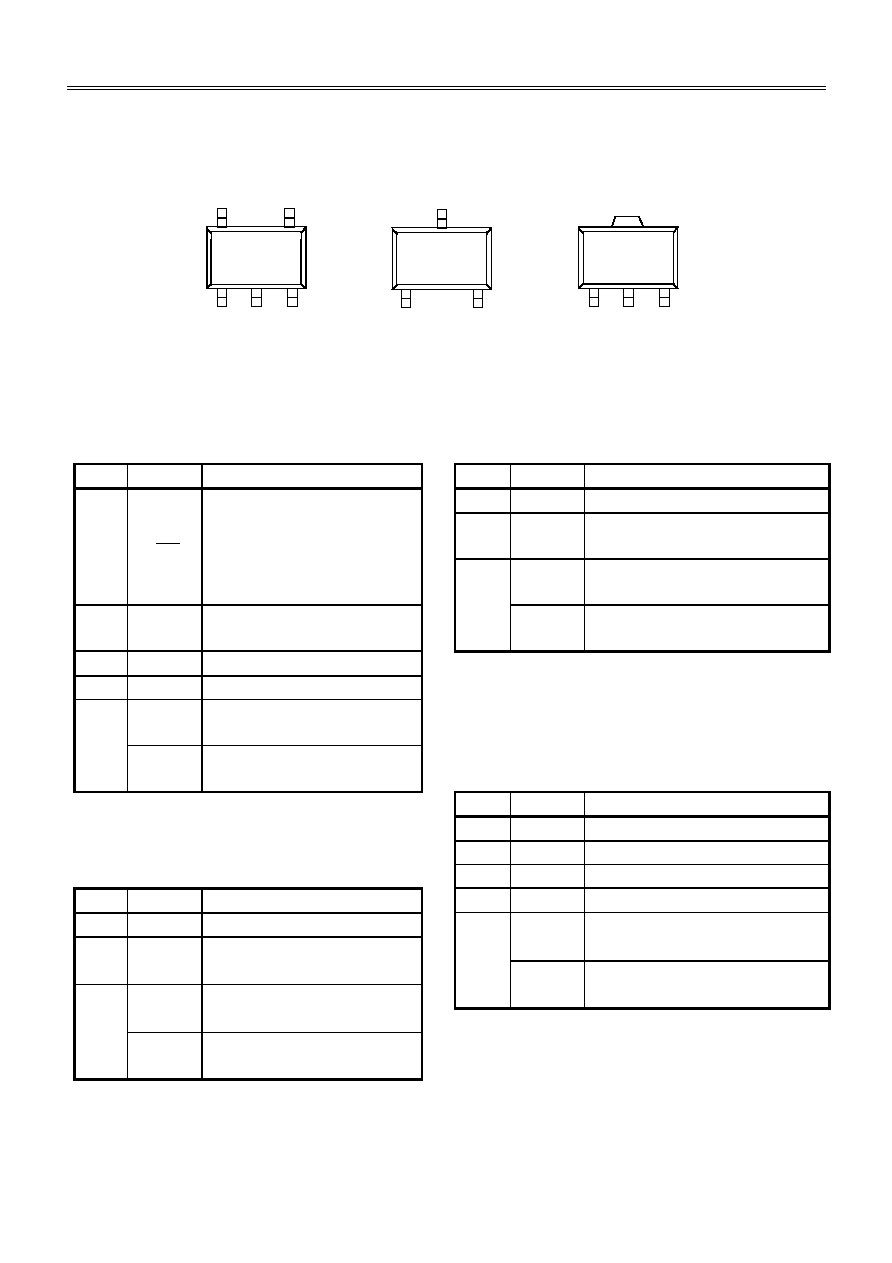
Pin Assignment
5
4
3
2
1
1
3
2
3
2
1
SOT-23-5
SOT-23-3
SOT-89-3
Top View
Top View
Top View
Figure 2. Pin Assignment
A type (with shutdown function)
B, C type (without shutdown function)
PKG: SOT-23-5
PKG: SOT-23-3
Pin No.
Pin Name
Functions
Pin No.
Pin Name
Functions
Shutdown pin
1
VOUT
Output voltage pin and IC power supply pin
1
ON/OFF
"H": Normal operation
(step-up operating)
2
VSS
GND pin
"L": Step-up stopped
(entire circuit stopped)
3
CONT
*1
External inductor connection pin
(S-8351 Series)
2
VOUT
Output voltage pin and IC power
supply pin
EXT
*2
External transistor connection pin
(S-8352 Series)
3
(N.C.)
4
VSS
GND pin
External inductor connection pin
(S-8351 Series)
External transistor connection pin
D type (V
DD
/V
OUT
separate type)
(S-8352 Series)
PKG: SOT-23-5
Pin No.
Pin Name
Functions
1
VOUT
Output voltage pin
C type (without shutdown function)
2
VDD
IC power supply pin
PKG: SOT-89-3
3
(N.C.)
Pin No.
Pin Name
Functions
4
VSS
GND pin
1
VSS
GND pin
External inductor connection pin
Output voltage pin and IC power
(S-8351 Series)
supply pin
External transistor connection pin
External inductor connection pin
(S-8352 Series)
(S-8351 Series)
External transistor connection pin
(S-8352 Series)
*1.
Open-drain output
*2.
CMOS output
5
CONT
*1
EXT
*2
CONT
*1
EXT
*2
CONT
*1
EXT
*2
3
2
VOUT
5
SMALL PACKAGE PFM CONTROL STEP-UP SWITCHING REGULATOR
S-8351/52 Series
Rev.1.0
_10
Seiko Instruments Inc.
6
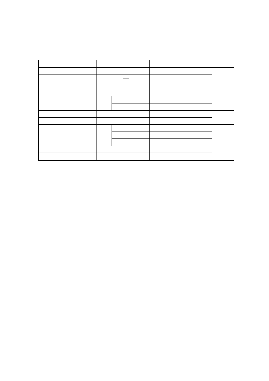
Absolute Maximum Ratings
Table 1. Absolute Maximum Ratings
(Unless otherwise specified, Ta
= 25įC)
Parameter
Symbol
Ratings
Unit
VOUT pin voltage
V
OUT
V
SS
- 0.3 to V
SS
+ 12
ON/OFF pin voltage (A type)
V
ON/OFF
V
SS
- 0.3 to V
SS
+ 12
VDD pin voltage (D type)
V
DD
V
SS
- 0.3 to V
SS
+ 12
CONT pin voltage
V
CONT
V
SS
- 0.3 to V
SS
+ 12
D type
V
SS
- 0.3 to V
DD
+ 0.3
Other than above
V
SS
- 0.3 to V
OUT
+ 0.3
CONT pin current
I
CONT
300
EXT pin current
I
EXT
Ī50
SOT-89-3
500
Power dissipation
P
D
SOT-23-5
250
mW
SOT-23-3
150
Operating temperature
T
opr
-40 to +85
Storage temperature
T
stg
-40 to +125
Caution Although the IC contains a static electricity protection circuit, static electricity or voltage
that exceeds the limit of the protection circuit should not be applied.
V
EXT
EXT pin voltage
V
įC
mA
SMALL PACKAGE PFM CONTROL STEP-UP SWITCHING REGULATOR
Rev.1.0
_10
S-8351/52 Series
Seiko Instruments Inc.
7
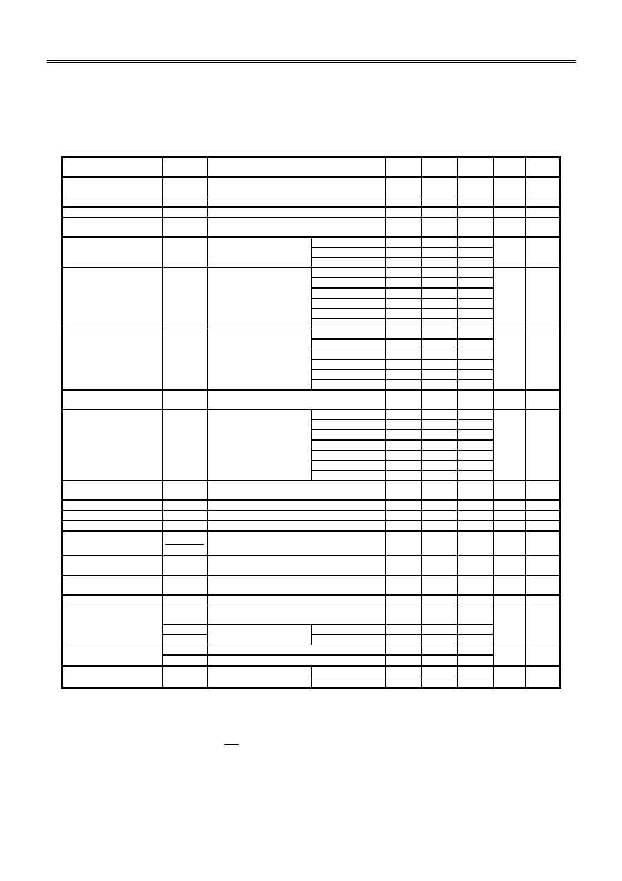
Electrical Characteristics
1-1. S-8351 Series
Table 2. Electrical Characteristics
(Unless otherwise specified, Ta
= 25įC)
Parameter
Symbol
Conditions
Min.
Typ.
Max.
Unit
Test
Circuit
Output voltage
V
OUT
V
OUT
(S)
◊ 0.976
V
OUT
(S)
V
OUT
(S)
◊ 1.024
V
1
Input voltage
V
IN
10
V
1
Operation start voltage
V
ST1
I
OUT
= 1 mA
0.9
V
1
Oscillation start voltage
V
ST2
No external parts, voltage applied to VOUT
CONT pulled up to VOUT via 300
resistor
0.8
V
2
S-8351x15 to 29
8.5
Input current without load
I
IN
I
OUT
= 0 mA
S-8351x30 to 49
9.0
ĶA
1
S-8351x50 to 65
9.5
S-8351x15 to 19
9.6
16.0
S-8351x20 to 29
15.7
26.2
S-8351x30 to 39
23.2
38.6
S-8351x40 to 49
32.0
53.3
S-8351x50 to 59
42.1
70.2
S-8351x60 to 65
54.9
91.5
S-8351x15 to 19
2.3
3.5
S-8351x20 to 29
2.5
3.8
S-8351x30 to 39
2.7
4.1
S-8351x40 to 49
2.9
4.4
S-8351x50 to 59
3.1
4.7
S-8351x60 to 65
3.3
5.1
Current consumption during
shutdown (A type)
I
SSS
Shutdown pin
= 0 V
0.5
ĶA
2
S-8351x15 to 19
50.2
91.2
S-8351x20 to 24
65.0
118.2
S-8351x25 to 29
78.5
142.7
Switching current
I
SW
V
CONT
= 0.4 V
S-8351x30 to 39
90.7
164.8
mA
2
S-8351x40 to 49
110.9
201.6
S-8351x50 to 59
125.7
228.6
S-8351x60 to 65
135.2
245.8
Switching transistor leakage
current
I
SWQ
No external parts, V
CONT
= V
OUT
= 10 V
Shutdown pin
= 0 V
0.5
ĶA
2
CONT limit voltage
V
CONTLMT
Apply to CONT pin, confirm oscillation stop
0.9
V
2
Line regulation
V
OUT1
V
IN
= V
OUT
(S)
◊ 0.4 to ◊ 0.6
30
60
mV
1
Load regulation
V
OUT2
I
OUT
= 10 ĶA to V
OUT
(S)/250
◊ 1.25
30
60
mV
1
Output voltage temperature
coefficient
V
OUT
Ta ∑ V
OUT
Ta
= -40įC to +85įC
Ī50
ppm/
įC
1
Maximum oscillation
frequency
f
OSC
V
OUT
= Output voltage ◊ 0.95, measure waveform at
CONT pin
90
100
110
kHz
2
Duty ratio 1
Duty1
V
OUT
= Output voltage ◊ 0.95, measure waveform at
CONT pin
70
75
80
%
2
Duty ratio 2 (A, B, D type)
Duty2
Measure waveform at CONT pin with light load
50
%
1
V
SH
V
OUT
= Output voltage ◊ 0.95, judge oscillation at
CONT pin
0.75
V
SL1
V
OUT
= Output voltage
◊ 0.95,
When V
OUT
1.5 V
0.3
V
SL2
judge stop at CONT pin
When V
OUT
< 1.5 V
0.2
Shutdown pin input
I
SH
Shutdown pin
= 10 V
-0.1
0.1
current (A type)
I
SL
Shutdown pin
= 0 V
-0.1
0.1
S-8351x30
86
S-8351x50
88
External parts
Coil:
CDRH6D28-101 (100
ĶH) from Sumida Corporation
Diode:
MA2Z748 (Schottky type) from Matsushita Electronic Components Co., Ltd .
Capacitor:
F93 (16 V, 47
ĶF tantalum type) from Nichicon Corporation)
V
IN
= V
OUT
(S)
◊ 0.6 applied, I
OUT
= V
OUT
(S) / 250
Shutdown function built-in type (A type): ON/OFF pin is connected to V
OUT
V
DD
/V
OUT
separate type (D type):
VDD pin is connected to VOUT pin
Remarks 1. V
OUT
(S) specified above is the set output voltage value, and V
OUT
is the typical value of the actual output voltage.
2. V
DD
/V
OUT
separate type (D type)
A step-up operation is performed from V
DD
= 0.8 V. However, 1.8 V V
DD
10 V is recommended to stabilize the output voltage and
oscillation frequency. (V
DD
1.8 V must be applied for products with a set value of less than 1.9 V.)
Current consumption 1
V
OUT
= Output voltage ◊ 0.95
I
SS1
ĶA
2
Current consumption 2
V
OUT
= Output voltage + 0.5
I
SS2
ĶA
2
Shutdown pin input
voltage (A type)
%
1
ĶA
2
Efficiency
EFFI
V
2

SMALL PACKAGE PFM CONTROL STEP-UP SWITCHING REGULATOR
S-8351/52 Series
Rev.1.0
_10
Seiko Instruments Inc.
8
2-1. S-8352 Series
Table 3. Electrical Characteristics
(Unless otherwise specified, Ta
= 25įC)
Parameter
Symbol
Conditions
Min.
Typ.
Max.
Unit
Test
Circuit
Output voltage
V
OUT
V
OUT
(S)
◊ 0.976
V
OUT
(S)
V
OUT
(S)
◊ 1.024
V
3
Input voltage
V
IN
10
V
3
Operation start voltage
V
ST1
I
OUT
= 1 mA
0.9
V
3
Oscillation start voltage
V
ST2
No external parts, voltage applied to VOUT
0.8
V
4
S-8352x15 to 19
7.4
12.3
S-8352x20 to 29
12.0
20.0
S-8352x30 to 39
17.8
29.6
S-8352x40 to 49
24.7
41.1
S-8352x50 to 59
32.7
54.5
S-8352x60 to 65
43.0
71.6
S-8352x15 to 19
2.3
3.5
S-8352x20 to 29
2.5
3.8
S-8352x30 to 39
2.7
4.1
S-8352x40 to 49
2.9
4.4
S-8352x50 to 59
3.1
4.7
S-8352x60 to 65
3.3
5.1
Current consumption during
shutdown (A type)
I
SSS
Shutdown pin
= 0 V
0.5
ĶA
4
S-8352x15 to 19
-3.5
-6.3
S-8352x20 to 24
-5.2
-9.4
S-8352x25 to 29
-6.8
-12.3
I
EXTH
V
EXT
= V
OUT
- 0.4 V
S-8352x30 to 39
-8.2
-14.9
mA
4
S-8352x40 to 49
-10.7
-19.4
S-8352x50 to 59
-12.5
-22.8
S-8352x60 to 65
-13.9
-25.2
S-8352x15 to 19
3.8
6.9
S-8352x20 to 24
5.6
10.2
S-8352x25 to 29
7.3
13.3
I
EXTL
V
EXT
= 0.4 V
S-8352x30 to 39
8.9
16.2
mA
4
S-8352x40 to 49
11.6
21.1
S-8352x50 to 59
13.7
25.0
S-8352x60 to 65
15.3
27.8
Line regulation
V
OUT1
V
IN
= V
OUT
(S)
◊ 0.4 to ◊ 0.6
30
60
mV
3
Load regulation
V
OUT2
I
OUT
= 10 ĶA to V
OUT
(S)/100
◊ 1.25
30
60
mV
3
Output voltage temperature
coefficient
V
OUT
Ta
∑ V
OUT
Ta
= -40įC to +85įC
Ī50
ppm/
įC
3
Maximum oscillation
frequency
f
OSC
V
OUT
= Output voltage ◊ 0.95, measure waveform at
EXT pin
90
100
110
kHz
4
Duty ratio 1
Duty1
V
OUT
= Output voltage ◊ 0.95, measure waveform at
EXT pin
70
75
80
%
4
Duty ratio 2 (A, B, D type)
Duty2
Measure waveform at EXT pin with light load
50
%
3
V
SH
V
OUT
= Output voltage ◊ 0.95, measure oscillation at
EXT pin
0.75
V
SL1
V
OUT
= Output voltage ◊ 0.95,
When V
OUT
1.5 V
0.3
V
4
V
SL2
judge stop at EXT pin
When V
OUT
< 1.5 V
0.2
Power off pin input
I
SH
Shutdown pin
= 10 V
-0.1
0.1
ĶA
4
current (A type)
I
SL
Shutdown pin
= 0 V
-0.1
0.1
S-8352x30
83
S-8352x50
85
External parts
Coil:
CDRH6D28-101 (100
ĶH) from Sumida Corporation
Diode:
MA2Z748 (Schottky type) from Matsushita Electronic Components Co. , Ltd.
Capacitor:
F93 (16 V, 47
ĶF tantalum type) from Nichicon Corporation
Transistor:
CPH3210 from Sanyo Electric Co., Ltd.
Base resistor (Rb):
1 k
Base capacitor (Cb): 2200 pF (ceramic type)
V
IN
= V
OUT
(S)
◊ 0.6 applied, I
OUT
= V
OUT
(S) / 100
Shutdown function built-in type (A type): ON/OFF pin is connected to V
OUT
V
DD
/V
OUT
separate type (D type):
VDD pin is connected to VOUT pin
Remarks 1. V
OUT
(S) specified above is the set output voltage value, and V
OUT
is the typical value of the actual output voltage.
2. V
DD
/V
OUT
separate type (D type)
A step-up operation is performed from V
DD
= 0.8 V. However, 1.8 V V
DD
10 V is recommended to stabilize the output voltage and
oscillation frequency. (V
DD
1.8 V must be applied for products with a set value of less than 1.9 V.)
Shutdown pin input
voltage (A type)
%
3
Efficiency
EXT pin output current
EFFI
Current consumption 1
V
OUT
= Output voltage ◊ 0.95
I
SS1
Current consumption 2
V
OUT
= Output voltage + 0.5
I
SS2
ĶA
4
ĶA
4
SMALL PACKAGE PFM CONTROL STEP-UP SWITCHING REGULATOR
Rev.1.0
_10
S-8351/52 Series
Seiko Instruments Inc.
9
Test Circuits
1.
VSS
CONT
V
-
+
-
+
(ON/OFF)
2.
3.
4.
300
VSS
V
-
+
-
+
Rb
EXT
VOUT
(VDD)
VOUT
(VDD)
(ON/OFF)
Cb
(ON/OFF)
VSS
VOUT
CONT
-
+
A
O
scil
l
os
co
pe
VSS
(ON/OFF)
-
+
A
O
scil
l
os
co
pe
EXT
(VDD)
VOUT
(VDD)
Figure 3. Test Circuits 1, 2, 3, and 4
SMALL PACKAGE PFM CONTROL STEP-UP SWITCHING REGULATOR
S-8351/52 Series
Rev.1.0
_10
Seiko Instruments Inc.
10
Operation
1. Step-up DC/DC Converter
The S-8351/52 Series is a DC/DC converter that uses a pulse frequency modulation method (PFM) and
features low current consumption. This series is an especially efficient DC/DC converter at an output
current of 100
ĶA or lower.
In conventional fixed-duty PFM DC/DC converters, although a low duty ratio allows a lower ripple voltage
when the current load is light, the efficiency is decreased when the output load current is large.
Conversely, a high duty ratio increases the output load current and efficiency, but increases the ripple
voltage when the output load current is low.
In the A, B, and D types, the duty ratio is automatically switched 75% when the output load current is
high to secure the load drive capability, and 50% when the output load current is low to control the load
drive capability to decrease pulse skipping. This suppresses a drop in the ripple frequency, enabling
control of the increase in the ripple voltage. The C type adopts a 75% fixed-duty PFM method. The
ripple voltage increases more than that of the duty switching type with the load is low, but the efficiency
is better.
In the A, B, and D types, the duty ratio is not rapidly changed, but rather smoothly switched in the
intermediate area between 50% and 75%. Therefore, fluctuation of the ripple voltage caused by duty
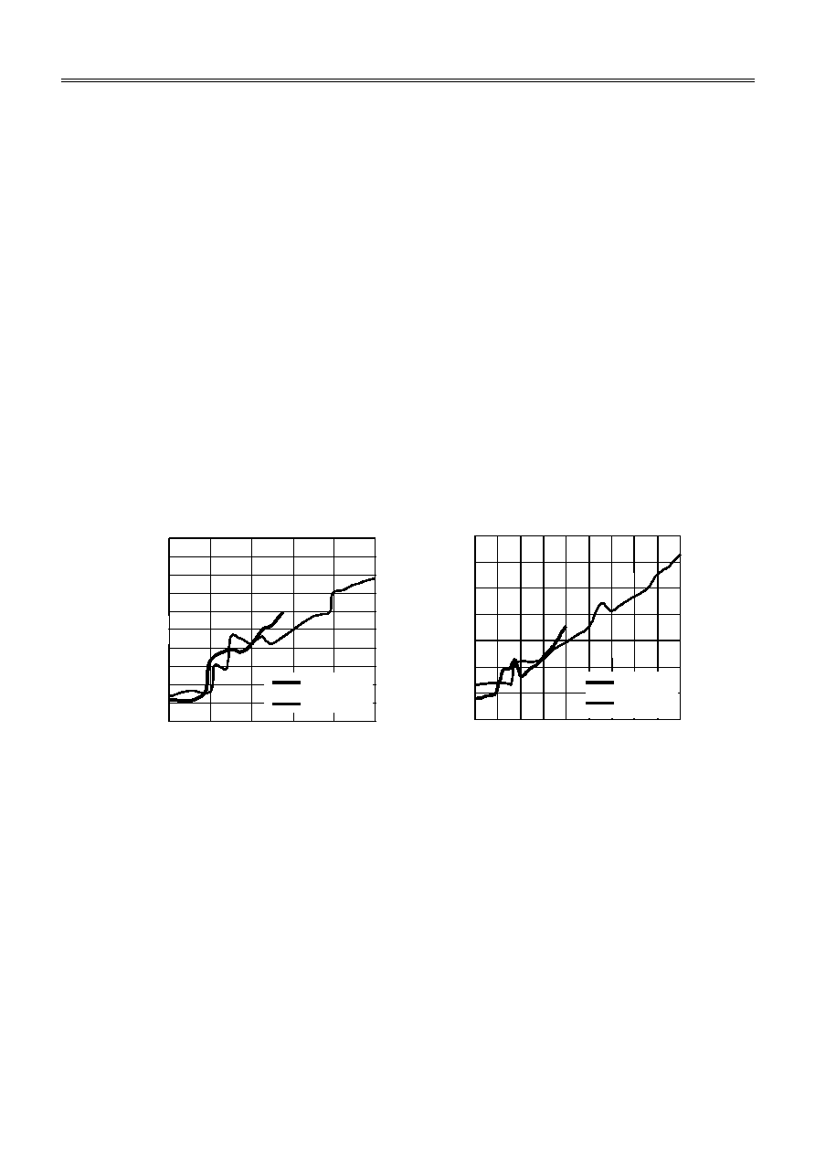
switching is minimized. Figures 4 and 5 show the ripple voltage characteristics versus the output
current. These figures show that the ripple voltage decreases as the output load current (I
OUT
) changes
from large to small. The ripple voltage becomes particularly small when I
OUT
is in the coil current
discontinuous region of 20 mA or less.
S-8351A30MC
Ta
= 25įC
0
10
20
30
40
50
60
70
80
90
100
0
20
40
60
80
100
I
OUT
(mA)
V
rp-p
(m
V
)
V
IN
= 1.5 V
V
IN
= 2 V
Ta
= 25įC
S-8351A50MC
0
20
40
60
80
100
120
140
0 20 40 60 80 100120140160180
I
OUT
(mA)
V
rp-p
(m
V
)
V
IN
= 2 V
V
IN
= 3 V
Figure 4. Ripple Voltage Characteristics
vs. Output Current (S-8351A30MC)
Figure 5. Ripple Voltage Characteristics vs.
Output Current (S-8351A50MC)
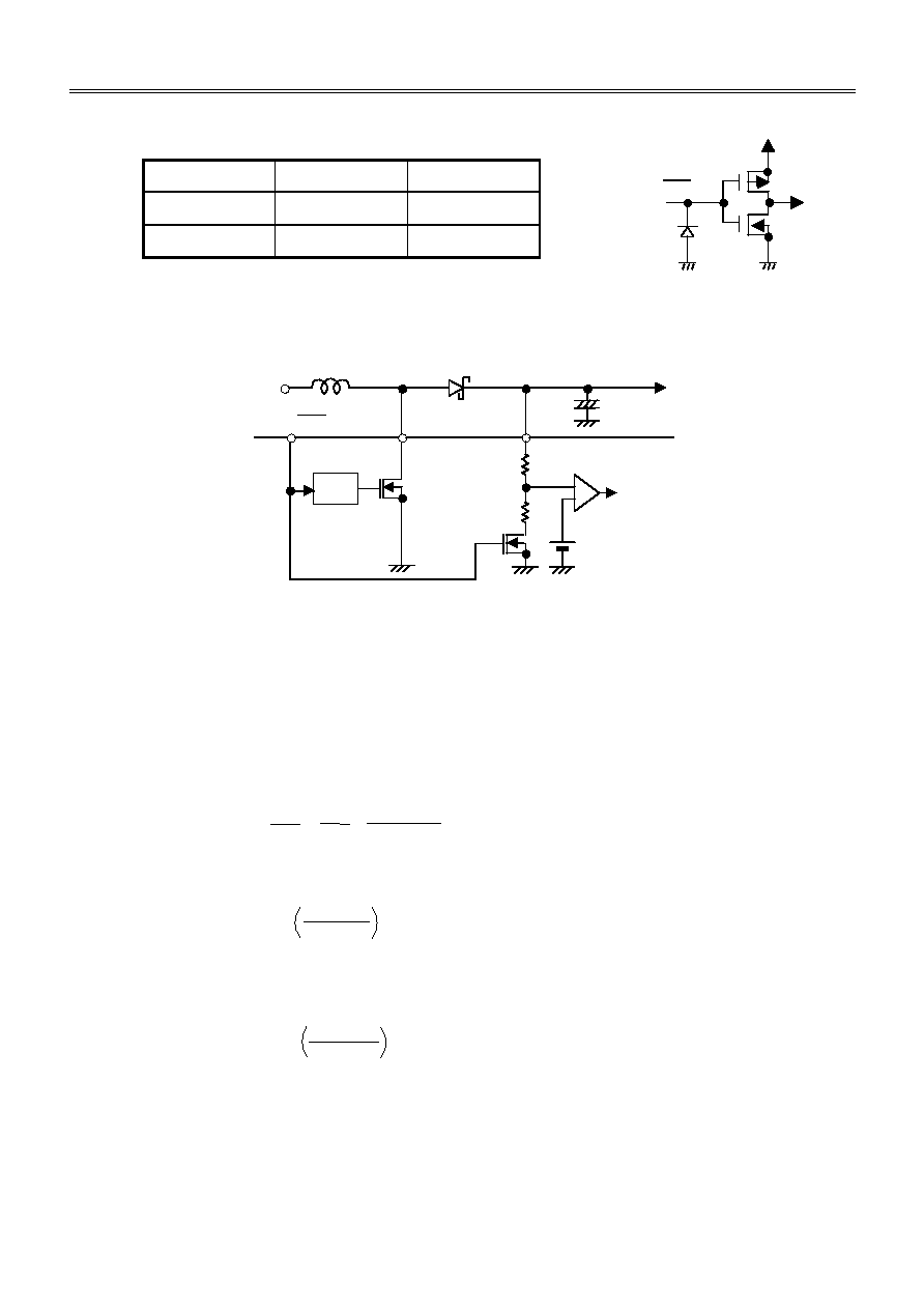
Shutdown pin: Stops or starts step-up operation.
(Only for product type A)
Setting the shutdown pin to the "L" level stops operation of all the internal circuits and reduces the
current consumption significantly.
DO NOT use the shutdown pin in a floating state because it has the structure shown in Figure 6
and is not pulled up or pulled down internally. DO NOT apply a voltage of between 0.3 V and 0.75
V to the shutdown pin because applying such a voltage increases the current consumption. If the
shutdown pin is not used, connect it to the VOUT pin.
The shutdown pin does not have hysteresis.
SMALL PACKAGE PFM CONTROL STEP-UP SWITCHING REGULATOR
Rev.1.0
_10
S-8351/52 Series
Seiko Instruments Inc.
11
Shutdown Pin
CR Oscillator
Output Voltage
"H"
Operating
Fixed
"L"
Stopped
V
IN
*
+
+
-
OSC
C
L
CONT
M1
V
IN
L
Di
ON/OFF
VOUT
The following are the basic equations [(1) through (7)] of the step-up switching regulator (see Figure 7).
Voltage at CONT pin at the moment M1 is turned ON (current (I
L
) flowing through L is zero), V
A
:
The change in I
L
over time:
Integration of the above equation (I
L
):
I
L
flows while M1 is ON (t
ON
). The time of t
ON
is determined by the oscillation frequency of OSC.
The peak current (I
PK
) after t
ON
:
The energy stored in L is represented by 1/2
∑ L (I
PK
)
2
.
When M1 is turned OFF (t
OFF
), the energy stored in L is emitted through a diode.
Then, the reverse voltage (V
L
) is generated:
Figure 6. Shutdown Pin Structure
VSS
VOUT
ON/OFF
(V
S
: Non-saturated voltage of M1)
V
A
= V
S
=
=
dI
L
dt
V
L
L
V
IN
- V
S
L
I
L
=
∑ t
V
IN
- V
S
L
I
PK
=
∑ t
ON
V
IN
- V
S
L
V
L
= (V
OUT
+ V
D
) - V
IN
(V
D
: Diode forward voltage)
* Voltage obtained by subtracting the voltage drop due to
the DC resistance of the inductor and the diode forward
voltage from V
IN
.
Figure 7. Step-Up Switching Regulator Circuit for Basic Equation
................................................................. (2)
............................................................................. (3)
...................................................................... (4)
............................................................................ (5)
................................................................................................... (1)

SMALL PACKAGE PFM CONTROL STEP-UP SWITCHING REGULATOR
S-8351/52 Series
Rev.1.0
_10
Seiko Instruments Inc.
12
The voltage at CONT pin rises only by V
OUT
+ V
D
.
The change in the current (I
L
) flowing through the diode into V
OUT
during t
OFF
:
Integration of the above equation is as follows:
During t
ON
, the energy is stored in L and is not transmitted to V
OUT
. When receiving the output current (I
OUT
) from
V
OUT
, the energy of the capacitor (C
L
) is consumed. As a result, the pin voltage of C
L
is reduced, and goes to the
lowest level after M1 is turned ON (t
ON
). When M1 is turned OFF, the energy stored in L is transmitted through
the diode to C
L
, and the voltage of C
L
rises rapidly. V
OUT
is a time function, and therefore indicates the maximum
value (ripple voltage: V
P-P
) when the current flowing through into V
OUT
and load current (I
OUT
) match.
Next, the ripple voltage is determined as follows:
I
OUT
vs. t
1
(time) from when M1 is turned OFF (after t
ON
) to when V
OUT
reaches the maximum level:
When M1 is turned OFF (t
OFF
), I
L
= 0 (when the energy of the inductor is completely transmitted)
:
Based on equation (7),
When substituting equation (10) for equation (9),
Electric charge
Q
1
which is charged in C
L
during t
1
:
When substituting equation (12) for equation (9):
A rise in voltage (V
P-P
) due to
Q
1
:
=
=
dI
L
dt
V
L
L
V
OUT
+ V
D
- V
IN
L
I
L
= I
PK
-
∑ t
L
V
OUT
+ V
D
- V
IN
I
OUT
= I
PK
-
∑ t
1
t
1
= (I
PK
- I
OUT
) ∑
V
OUT
+ V
D
- V
IN
L
V
OUT
+ V
D
- V
IN
L
=
V
OUT
+ V
D
- V
IN
L
I
PK
t
OFF
t
1
= t
OFF
-
∑ t
OFF
I
PK
I
OUT
Q
1
= I
L
dt = I
PK
∑ dt -
∑ tdt
= I
PK
∑ t
1
-
∑
t
1
2
V
OUT
+ V
D
- V
IN
L
2
1
t
1
0
V
OUT
+ V
D
- V
IN
L
0
t
1
0
t
1
Q
1
= I
PK
-
(I
PK
- I
OUT
) ∑ t
1
=
∑ t
1
2
1
2
I
PK
+ I
OUT
V
P-P
=
=
∑
∑ t
1
C
L
Q
1
C
L
1
2
I
PK
+ I
OUT
.......................................................... (8)
........................................................... (9)
.............................................................................. (11)
...................................................................... (6)
............................................ (13)
........................................................................ (7)
........................................................................ (10)
.................................................. (12)
.................................................... (14)

SMALL PACKAGE PFM CONTROL STEP-UP SWITCHING REGULATOR
Rev.1.0
_10
S-8351/52 Series
Seiko Instruments Inc.
13
When taking into consideration I
OUT
to be consumed during t
1
and the ESR (Equivalent Series Resistance) of C
L
,
namely R
ESR
:
When substituting equation (11) for equation (15):
Therefore to reduce the ripple voltage, it is important that the capacitor connected to the output pin has a large
capacity and a small ESR.
V
P-P
=
=
∑
∑ t +
∑ R
ESR
-
C
L
Q
1
C
L
1
2
I
PK
+ I
OUT
C
L
I
OUT
∑ t
1
2
I
PK
+ I
OUT
1
V
P-P
=
∑
+
∑ R
ESR
2I
PK
(I
PK
- I
OUT
)
2
C
L
t
OFF
2
I
PK
+ I
OUT
............. (15)
............................................ (16)

SMALL PACKAGE PFM CONTROL STEP-UP SWITCHING REGULATOR
S-8351/52 Series
Rev.1.0
_10
Seiko Instruments Inc.
14
External Part Selection
1. Inductor
To minimize the loss due to inductor DC resistance, select an inductor with the smallest possible DC
resistance (less than 1
). Set the inductance value to around 22 ĶH to 1 mH.
To make the average value of the output voltage (V
OUT
) constant, it is necessary to supply the energy
corresponding to the output current (I
OUT
) from the inductor. The amount of charge required for I
OUT
is I
OUT
◊ (t
ON
+ t
OFF
). Because the inductor can supply energy only during t
OFF
, the charge is obtained by
integrating equation (7) with 0
t
OFF
, namely,
When the oscillation duty ratio of OSC is 75%, I
PK
= 8 I
OUT
. Therefore, an I
PK
current which is eight times
I
OUT
flows into transistor M1.
The S-8351 Series includes a switching current controller which monitors the current flowing into the CONT
pin by the voltage (CONT control voltage) and controls the current. This controller prevents destruction of
the IC due to excess current.
If an inductor with a large L value is selected, both I
PK
and I
OUT
decrease. Since the energy stored in the
inductor is equal to Ĺ L (I
PK
)
2
, the energy decreases because I
PK
decreases in steps of squares offsetting
the increase of L. As a result, stepping up at a low voltage becomes difficult and the minimum operating
input voltage becomes high. However, the DC resistance loss of L and the M1 transistor decreases by the
amount I
PK
decreased, and the inductance efficiency improves.
On the other hand, if an inductor with a smaller L value is selected, both I
PK
and I
OUT
increase. Accordingly,
the minimum operating input voltage becomes low but the inductance efficiency deteriorates.
Caution An excessively large I
PK
may cause magnetic saturation for some core materials, leading
to the destruction of the IC. Use a core with material that satisfies I
sat
>
>
>
> I
PK
(I
sat
:
Level of
current that causes magnetic saturation).
2. Diode
Use an external diode that meets the following requirements:
∑ Low forward voltage:
V
F
< 0.3V
∑ High switching speed:
500 ns max.
∑ Reverse voltage:
V
OUT
+ V
F
or more
∑ Rated current:
I
PK
or more
t
OFF
Thus,
t
OFF
= I
OUT
◊ (t
ON
+ t
OFF
) ............................................................. .(17)
I
PK
= 2 I
OUT
................................................................. (18)
2
I
PK
2
I
PK
t
OFF
t
ON
+ t
OFF
SMALL PACKAGE PFM CONTROL STEP-UP SWITCHING REGULATOR
Rev.1.0
_10
S-8351/52 Series
Seiko Instruments Inc.
15
3. Capacitors (C
IN
, C
L
)
A capacitor at the input side (C
IN
) improves the efficiency by reducing the power impedance and stabilizing
the input current. Select the C
IN
value according to the impedance of the power supply used. The
capacitor value should be around 10
ĶF.
A capacitor at the output side (C
L
) is used for smoothing the ripple voltage. Therefore, select a capacitor
with a small ESR (Equivalent Series Resistance) and a large capacitance. The capacitor value should be
10
ĶF min. A tantalum electrolytic capacitor and an organic semiconductor capacitor are especially
recommended because of their superior low-temperature and leakage current characteristics.
4. External transistor (S-8352 Series)
For the S-8352 Series, connecting an external transistor increases the output current. A bipolar (NPN)
transistor or an enhancement (Nch) MOS FET transistor can be used as the external transistor.
4.1 Bipolar transistor
A circuit example using a bipolar transistor (NPN), the CPH3210 (h
FE
= 200 to 560) from Sanyo, is shown
in Figure 12 and 13. The h
FE
and R
b
values of the bipolar transistor determine the driving capacity to
increase the output current using a bipolar transistor. A peripheral circuit example of the transistor is
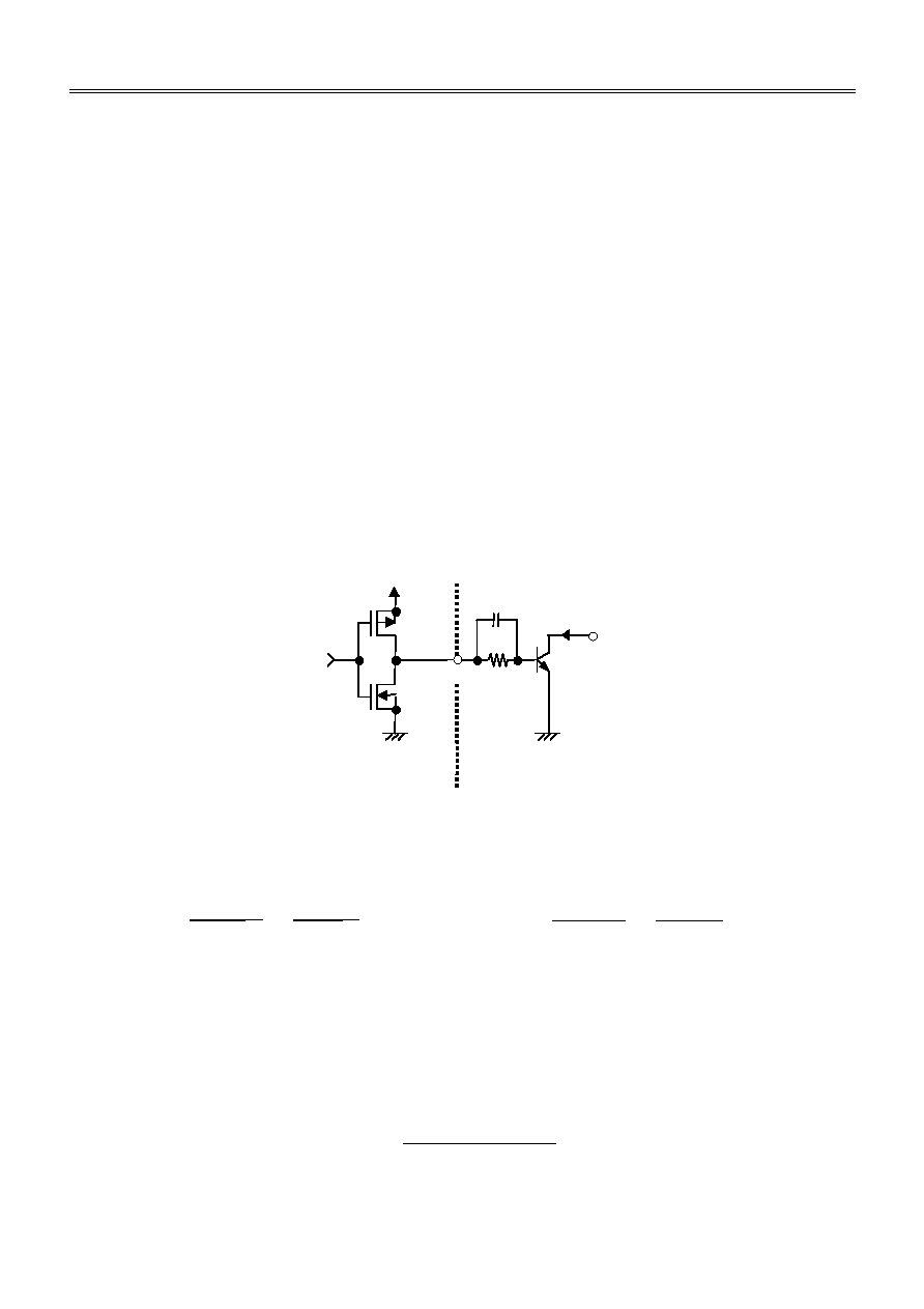
shown in Figure 8.
I
PK
EXT
Nch
VOUT
Pch
Rb
S-8352
2200 pF
1 k
Cb
The recommended R
b
value is around 1 k
. Actually, determine the required base current Ib from the
bipolar transistor h
FE
assuming I
b
= I
PK
/h
FE
, and select the smaller R
b
value:
I
b
V
OUT
- 0.7
I
EXTH
0.4
R
b
=
-
I
b
V
DD
- 0.7
I
EXTH
0.4
R
b
=
-
(
)
A small Rb value can increase the output current, but reduces the efficiency. Since a current may flow on
the pulse and the voltage may drop due to wiring resistance or other factors, a test should be performed to
determine the optimum value.
If the speed-up capacitor (C
b
) is inserted in parallel with the R
b
resistor as shown in Figure 8, the switching
loss is decreased and the efficiency is improved.
Select the C
b
value according to:
1
2 ∑ Rb ∑ f
OSC
∑ 0.7
C
b
However, the best C
b
value varies depending on the characteristics of the bipolar transistor to be used, so
determine the optimum value via testing.
Figure 8. External Transistor Peripheral Circuit

SMALL PACKAGE PFM CONTROL STEP-UP SWITCHING REGULATOR
S-8351/52 Series
Rev.1.0
_10
Seiko Instruments Inc.
16
4.2 Enhancement MOS FET type
A large current may flow during startup, depending on the MOS FET selection. The S-8352 Series does
not feature overcurrent protection for the external MOS FET, so perform sufficient evaluation using the
devices to be actually used.
Since the on-resistance of the MOS FET might affect the output current as well as the efficiency, the
threshold voltage should be low. When the output voltage is as low as 2.0 V, like in the S-8352A20, the
circuit operates only when the MOS FET has a threshold voltage lower than 2.0 V.
5. V
DD
/V
OUT
separate type (S-8351/52 Series D type)
The S-8351/52 Series D type provides separate internal circuit power supply and output voltage setting
pins (VDD and VOUT, respectively) , making it ideal for the following applications.
<1> Changing the output voltage value using an external resistor
<2> Setting a high output voltage value, such as
+15 V
In this case, observe the following points when using this product.
i) A step-up operation is performed from V
DD
= 0.8 V. However, 1.8 V V
DD
10 V is recommended
to stabilize the output voltage and oscillation frequency. (V
DD
1.8 V must be applied for products
with a set value of less than 1.9 V.)
If VDD is within the above range, the VDD pin can be connected to either the input voltage pin VIN
or the output pin VOUT .
ii) There is impedance between the VOUT pin and VSS pin in the IC, so select external resistors R
a
and R
b
so that there are no negative effects when setting the output voltage.
The internal resistance between the VOUT and VSS pins are as follows.
<1> S-835XD18
5.6 M
to 14.9 M
<2> S-835XD20
5.2 M
to 12.3 M
<3> S-835XD50
3.8 M
to 10.4 M
iii) If unstable operation such as oscillation of the output voltage occurs, add capacitor C
c
in parallel
with the R
a
resistor. Determine the C
c
value using the following equation.
2 ∑ ∑ R
a
∑ 20 kHz
1
C
c
(F) =
V
OUT
EXT
VOUT
-
+
(ON/OFF)
VSS
+
-
Figure 9 is a circuit example using a MOS FET
transistor (N-channel).
An N-channel power MOS FET should be used for
MOS FET. In particular, the EXT pin of the S-8352
can drive a MOS FET with a gate capacitance of
around 1000 pF. Because the gate voltage and
current of the external power MOS FET are
supplied from the stepped-up output voltage V
OUT
,
the MOS FET is driven more effectively.
Figure 9. Circuit Example Using MOS FET
SMALL PACKAGE PFM CONTROL STEP-UP SWITCHING REGULATOR
Rev.1.0
_10
S-8351/52 Series
Seiko Instruments Inc.
17
Standard Circuits
(1) S-8351 Series A, B, C type
Figure 11. Standard Circuit (2)
(2) S-8351 Series D type
Figure 10. Standard Circuit (1)
C
L
PFM
controller
V
REF
+
-
Protection
circuit
L
CONT
SD
VOUT
V
IN
VSS
(ON/OFF)
-
+
-
+
C
IN
C
L
PFM
controller
V
REF
+
-
Protection
circuit
L
CONT
SD
IC internal
power supply
VDD
C
C
R
b
R
a
VOUT
V
IN
VSS
-
+
-
+
C
IN

SMALL PACKAGE PFM CONTROL STEP-UP SWITCHING REGULATOR
S-8351/52 Series
Rev.1.0
_10
Seiko Instruments Inc.
18
(3) S-8352 Series A, B, C type
Figure 13. Standard Circuit (4)
(4) S-8352 Series D type
Figure 12. Standard Circuit (3)
C
IN
C
L
PFM
controller
V
REF
+
-
SD
VOUT
VSS
-
+
2200 pF
1 k
V
IN
-
+
(ON/OFF)
EXT
C
L
-
+
C
c
R
b
R
a
C
IN
PFM
controller
V
REF
+
-
IC internal power
supply
VDD
SD
VSS
2200 pF
1 k
V
IN
-
+
EXT
Caution The above connection diagram and constants do not guarantee correct operation.
Perform sufficient evaluation using the actual application to set the constants.
SMALL PACKAGE PFM CONTROL STEP-UP SWITCHING REGULATOR
Rev.1.0
_10
S-8351/52 Series
Seiko Instruments Inc.
19
Power Dissipation of Package
0
50
100
150
600
400
200
0
Power dissipation
P
D
(mW)
Ambient temperature Ta (įC)
SOT-23-3
SOT-89-3
SOT-23-5
Figure 12. Power Dissipation of Package (Before Mounting)
Cautions
Mount the external capacitors, diode, and coil as close as possible to the IC.
Ripple voltage and spike noise occur in switching regulators. Because they largely depend on the coil and
the capacitor used, check these parameters using the actually mounted model.
Seiko Instruments shall not be responsible for any patent infringement by products including S-8351/8352
Series in connection with the method of using S-8351/8352 Series in such products, the specification of
such products, or the country of destination thereof.
Ensure that the dissipation of the switching transistor (especially at high temperatures) does not exceed the
allowable power dissipation of the package.
When the impedance of the power supply is high, the shutdown pin is switched from "L" to "H", or VIN is
connected to the power supply, note that the power supply voltage drops temporarily because a rush
current flows into the power supply.
∑
∑
∑
∑
∑
SMALL PACKAGE PFM CONTROL STEP-UP SWITCHING REGULATOR
S-8351/52 Series
Rev.1.0
_10
Seiko Instruments Inc.
20
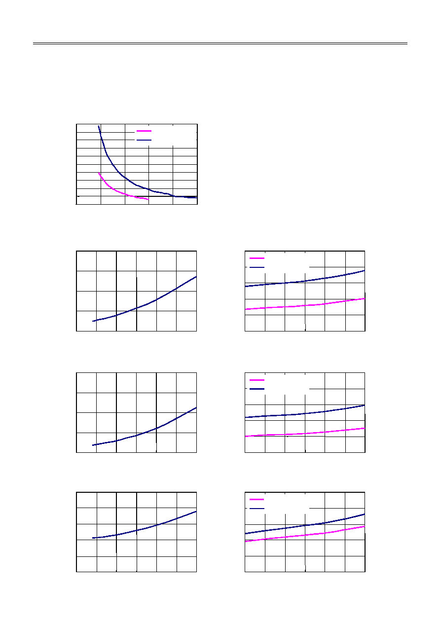
Characteristics (All Data Indicates Typical Values)
1. Current consumption vs. Power supply voltage
∑ Power supply input current no load
(Ta = 25įC)
0
5
10
15
20
25
30
35
40
45
50
0
1
2
3
4
5
V
IN
[V]
I
IN
[ĶA]
S-8351A30MC
S-8351A50MC
∑ I
SS1
vs. V
OUT
, Ta
S-8351A
(Ta = 25įC)
0
20
40
60
80
I
SS1
[ĶA]
V
OUT
[V]
1
2
3
4
5
6
7
0
20
30
40
50
I
SS1
[ĶA]
10
-50
-25
0
25
50
75
100
Ta [įC]
S-8351A30MC
S-8351A50MC
S-8351A
S-8352A
(Ta = 25įC)
0
20
40
60
80
I
SS1
[ĶA]
V
OUT
[V]
1
2
3
4
5
6
7
0
20
30
40
50
I
SS1
[ĶA]
10
-50
-25
0
25
50
75
100
Ta [įC]
S-8352A
S-8352A30MC
S-8352A50MC
(Ta = 25įC)
0
1
2
3
4
I
SS2
[ĶA]
V
OUT
[V]
1
2
3
4
5
6
7
I
SS2
[ĶA]
-50
-25
0
25
50
75
100
Ta [įC]
∑ I
SS2
vs. V
OUT
, Ta
5
S-8351A30MC
S-8351A50MC
0
1
2
3
4
5

SMALL PACKAGE PFM CONTROL STEP-UP SWITCHING REGULATOR
Rev.1.0
_10
S-8351/52 Series
Seiko Instruments Inc.
21
100
110
120
130
140
-50
-25
0
25
50
75
100
Ta [įC]
f
OSC
[kHz]
Duty1
[%]
10
15
20
25
30
35
0
10
20
30
40
0
50
0
1
2
3
4
5
6
7
V
OUT
[V]
I
SW
[mA]
70
72
74
76
78
80
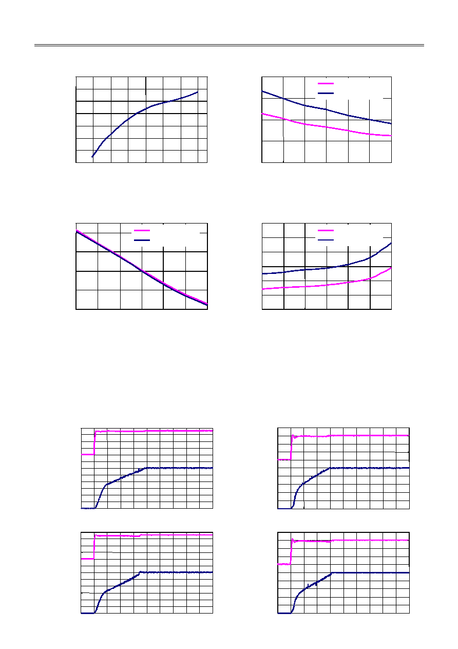
2. Oscillation frequency, duty ratio vs. Temperature
80
90
S-8351A30MC
S-8351A50MC
-50
-25
0
25
50
75
100
Ta [įC]
Duty2
[%]
45
47
49
51
53
55
-50
-25
0
25
50
75
100
Ta [įC]
S-8351A30MC
S-8351A50MC
S-8351A30MC
S-8351A50MC
3. Switching current vs. Output voltage, temperature
∑ I
SW
vs. V
OUT
, Ta
100
150
200
250
300
(Ta = 25
įC
)
I
SW
[mA]
-50
-25
0
25
50
75
100
Ta [įC]
S-8351A30MC
S-8351A50MC
0
50
200
250
300
350
400
150
100
4. EXT pin output current vs. Output voltage, temperature
∑ I
EXTH
vs. V
OUT
, Ta
(Ta = 25
įC
)
I
EXTH
[mA]
I
EXTH
[mA]
0
1
2
3
4
5
6
7
V
OUT
[V]
0
5
-50
-25
0
25
50
75
100
Ta [įC]
S-8352A30MC
S-8352A50MC
SMALL PACKAGE PFM CONTROL STEP-UP SWITCHING REGULATOR
S-8351/52 Series
Rev.1.0
_10
Seiko Instruments Inc.
22
10
15
20
25
30
35
0
10
20
30
40
∑ I
EXTL
vs. V
OUT
, Ta
(T
a
= 25
įC
)
I
EXTL
[mA]
I
EXTL
[mA]
0
1
2
3
4
5
6
7
V
OUT
[V]
0
5
-50
-25
0
25
50
75
100
Ta [įC]
S-8352A30MC
S-8352A50MC
0.6
0.7
0.8
0.9
1.0
0.4
0.5
0.6
0.7
0.8
5. Operation start voltage, retention voltage vs. Temperature
∑ V
ST1
vs. Ta
V
ST1
[V]
V
HLD
[V]
-50
-25
0
25
50
75
100
Ta [įC]
∑ V
HLD
vs. Ta
-50
-25
0
25
50
75
100
Ta [įC]
0.2
0.3
S-8351A30MC
S-8351A50MC
S-8351A30MC
S-8351A50MC
Reference Data (1)
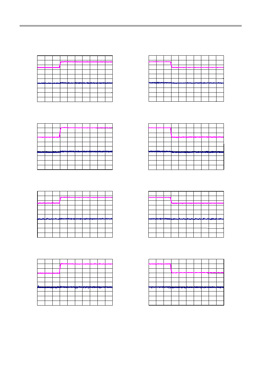
1. Transient response characteristics
The conditions for external parts are the same as those specified in the electrical characteristics.
1.1 Power-on (Ta
= 25įC)
t (0.2 ms/div)
S-8351A30MC
V
IN
= 0 1.8 V, R
L
= 250
Input
voltage
(0.5 V/div)
Output
voltage
(0.5 V/div)
0 V
0 V
1.8 V
3 V
t (0.2 ms/div)
S-8351A50MC
V
IN
= 0 3 V, R
L
= 250
Input
voltage
(1 V/div)
Output
voltage
(1 V/div)
0 V
0 V
3 V
5 V
t (0.2 ms/div)
S-8352A30MC
V
IN
= 0 1.8 V, R
L
= 250
Input
voltage
(0.5 V/div)
Output
voltage
(0.5 V/div)
0 V
0 V
1.8 V
3 V
t (0.2 ms/div)
S-8352A50MC
V
IN
= 0 3 V, R
L
= 250
Input
voltage
(1 V/div)
Output
voltage
(1 V/div)
0 V
0 V
3 V
5 V
SMALL PACKAGE PFM CONTROL STEP-UP SWITCHING REGULATOR
Rev.1.0
_10
S-8351/52 Series
Seiko Instruments Inc.
23
1.2 Power supply voltage fluctuation (Ta
= 25įC)
S-8351A30MC
V
IN
= 1.2 1.8 V, R
L
= 250
S-8351A30MC
V
IN
= 1.8 1.2 V, R
L
= 250
t (0.1 ms/div)
t (0.1 ms/div)
S-8351A50MC
V
IN
= 2 3 V, R
L
= 250
S-8351A50MC
V
IN
= 3 2 V, R
L
= 250
t (0.1 ms/div)
t (0.1 ms/div)
S-8352A30MC
V
IN
= 1.2 1.8 V, R
L
= 250
S-8352A30MC
V
IN
= 1.8 1.2 V, R
L
= 250
t (0.1 ms/div)
t (0.1 ms/div)
S-8352A50MC
V
IN
= 2 3 V, R
L
= 250
S-8352A50MC
V
IN
= 3 2 V, R
L
= 250
t (0.1 ms/div)
t (0.1 ms/div)
Input
voltage
(0.5 V/div)
1.2 V
Output
voltage
(0.1 V/div)
1.8 V
3 V
1.2 V
3 V
3 V
5 V
2 V
5 V
1.8 V
3 V
1.2 V
3 V
2 V
5 V
3 V
5 V
1.8 V
Input
voltage
(0.5 V/div)
Output
voltage
(0.1 V/div)
Input
voltage
(0.5 V/div)
2 V
Output
voltage
(0.1 V/div)
3 V
Input
voltage
(0.5 V/div)
Output
voltage
(0.1 V/div)
Input
voltage
(0.5 V/div)
1.2 V
Output
voltage
(0.1 V/div)
1.8 V
Input
voltage
(0.5 V/div)
Output
voltage
(0.1 V/div)
Input
voltage
(0.5 V/div)
2 V
Output
voltage
(0.1 V/div)
3 V
Input
voltage
(0.5 V/div)
Output
voltage
(0.1 V/div)

SMALL PACKAGE PFM CONTROL STEP-UP SWITCHING REGULATOR
S-8351/52 Series
Rev.1.0
_10
Seiko Instruments Inc.
24
1.3 Load current fluctuation (Ta
= 25įC)
S-8351A30MC
V
IN
= 1.8 V, I
OUT
= 10 ĶA 12 mA
S-8351A30MC
V
IN
= 1.8 V, I
OUT
= 12 mA 10 ĶA
I
OUT
= 12 mA
I
OUT
= 10 ĶA
t (0.1 ms/div)
t (0.1 ms/div)
S-8351A50MC
V
IN
= 3 V, I
OUT
= 10 ĶA 20 mA
S-8351A50MC
V
IN
= 3 V, I
OUT
= 20 mA 10 ĶA
I
OUT
= 20 mA
I
OUT
= 10 ĶA
t (0.1 ms/div)
t (0.1 ms/div)
S-8352A30MC
V
IN
= 1.8 V, I
OUT
= 10 ĶA 12 mA
S-8352A30MC
V
IN
= 1.8 V, I
OUT
= 12 mA 10 ĶA
I
OUT
= 12 mA
I
OUT
= 10 ĶA
t (0.1 ms/div)
t (0.1 ms/div)
S-8352A50MC
V
IN
= 3 V, I
OUT
= 10 ĶA 20 mA
S-8352A50MC
V
IN
= 3 V, I
OUT
= 20 mA 10 ĶA
I
OUT
= 20 mA
I
OUT
= 10 ĶA
t (0.1 ms/div)
t (0.1 ms/div)
Output
current
Output
voltage
(0.1 V/div)
3 V
3 V
5 V
5 V
3 V
3 V
5 V
5 V
Output
current
Output
voltage
(0.1 V/div)
Output
current
Output
voltage
(0.1 V/div)
Output
current
Output
voltage
(0.1 V/div)
Output
current
Output
voltage
(0.1 V/div)
Output
current
Output
voltage
(0.1 V/div)
Output
current
Output
voltage
(0.1 V/div)
Output
current
Output
voltage
(0.1 V/div)

SMALL PACKAGE PFM CONTROL STEP-UP SWITCHING REGULATOR
Rev.1.0
_10
S-8351/52 Series
Seiko Instruments Inc.
25
1.4 Shutdown pin response (Ta
= 25įC)
S-8351A30MC
V
IN
= 1.8 V, R
L
= 250
S-8351A50MC
V
IN
= 3 V, R
L
= 250
OFF
ON
OFF
ON
t (0.1 ms/div)
t (0.1 ms/div)
S-8352A30MC
V
IN
= 1.8 V, R
L
= 250
S-8352A50MC
V
IN
= 3 V, R
L
= 250
OFF
ON
OFF
ON
t (0.1 ms/div)
t (0.1 ms/div)
Reference Data (2)
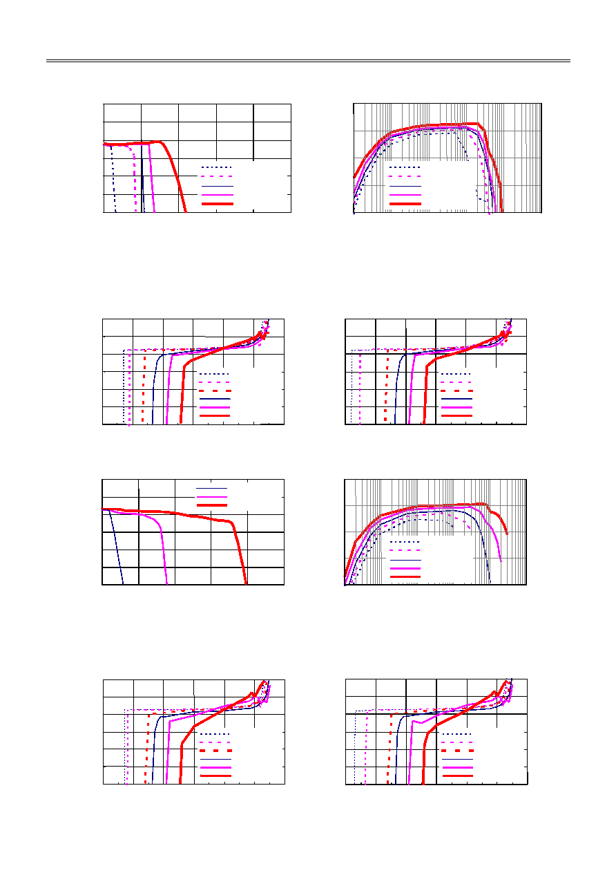
The following shows the step-up characteristics when the coils in the table below are used for reference.
Table 4
Model
Manufacturer
L Value
DC
Resistance
Current
Rating
CDRH6D28-220
Sumida Corporation
22
ĶH
0.128
1200 mA
CDRH6D28-470
Sumida Corporation
47
ĶH
0.238
800 mA
CDRH6D28-101
Sumida Corporation
100
ĶH
0.535
540 mA
CDRH125-221
Sumida Corporation
220
ĶH
0.4
800 mA
CXLP120-470
Sumitomo Special Metals Co., Ltd
47
ĶH
0.95
450 mA
CXLP120-101
Sumitomo Special Metals Co., Ltd
100
ĶH
2.5
200 mA
1. S-8351A30MC (built-in, V
OUT
=
=
=
= 3 V)
1-1 CDRH6D28-470 (47
ĶH), Ta = 25įC
2.8
2.9
3.0
3.1
(b) Input voltage vs. Output voltage
(input voltage stepped down)
(a) Input voltage vs. Output voltage
(input voltage stepped up)
Input voltage V
IN
[V]
O
u
tput v
o
lt
age V
OUT
[V]
2
3
4
1
0
I
OUT
= 0.1 mA
I
OUT
= 1 mA
I
OUT
= 10 mA
I
OUT
= 20 mA
I
OUT
= 50 mA
I
OUT
= 100 mA
3.2
2.6
2.7
2.8
2.9
3.0
3.1
Input voltage V
IN
[V]
O
u
tput v
o
lt
age V
OUT
[V]
2
3
4
1
0
I
OUT
= 0.1 mA
I
OUT
= 1 mA
I
OUT
= 10 mA
I
OUT
= 20 mA
I
OUT
= 50 mA
I
OUT
= 100 mA
3.2
2.6
2.7
ON/OFF
voltage
Output
voltage
(0.3 V/div)
3 V
3 V
5 V
5 V
ON/OFF
voltage
Output
voltage
(0.5 V/div)
ON/OFF
voltage
Output
voltage
(0.3 V/div)
ON/OFF
voltage
Output
voltage
(0.5 V/div)

SMALL PACKAGE PFM CONTROL STEP-UP SWITCHING REGULATOR
S-8351/52 Series
Rev.1.0
_10
Seiko Instruments Inc.
26
1-2 CDRH6D28-101 (100
ĶH), Ta = 25įC
1-3 CXLP120-101 (100
ĶH), Ta = 25įC
2.8
2.9
3.0
3.1
(d) Efficiency vs. Output current
(c) Output current vs. Output voltage
Output current
I
OUT
[mA]
O
u
tput v
o
lt
age V
OU
T
[V]
100
150
200
50
0
V
IN
= 1.0 V
V
IN
= 1.5 V
V
IN
= 1.8 V
V
IN
= 2.0 V
V
IN
= 2.5 V
3.2
2.6
2.7
250
50
60
70
80
E
ffi
c
i
e
n
c
y
[%]
Output current
I
OUT
[mA]
1
10
100
1000
0.1
0.01
90
V
IN
= 1.0 V
V
IN
= 1.5 V
V
IN
= 1.8 V
V
IN
= 2.0 V
V
IN
= 2.5 V
2.8
2.9
3.0
3.1
(b) Input voltage vs. Output voltage
(input voltage stepped down)
(a) Input voltage vs. Output voltage
(input voltage stepped up)
Input voltage V
IN
[V]
O
u
t
put
vol
t
a
ge
V
OU
T
[V]
2
3
4
1
0
I
OUT
= 0.1 mA
I
OUT
= 1 mA
I
OUT
= 10 mA
I
OUT
= 20 mA
I
OUT
= 50 mA
I
OUT
= 100 mA
3.2
2.6
2.7
2.8
2.9
3.0
3.1
Input voltage V
IN
[V]
O
u
t
put
vol
t
a
ge
V
OU
T
[V]
2
3
4
1
0
I
OUT
= 0.1 mA
I
OUT
= 1 mA
I
OUT
= 10 mA
I
OUT
= 20 mA
I
OUT
= 50 mA
I
OUT
= 100 mA
3.2
2.6
2.7
2.8
2.9
3.0
3.1
(d) Efficiency vs. Output current
(c) Output current vs. Output voltage
Output current
I
OUT
[mA]
O
u
tput v
o
lt
age V
OU
T
[V]
100
150
200
50
0
V
IN
= 1.0 V
V
IN
= 1.5 V
V
IN
= 1.8 V
V
IN
= 2.0 V
V
IN
= 2.5 V
3.2
2.6
2.7
250
50
60
70
80
E
ffi
c
i
e
n
c
y
[%]
Output current
I
OUT
[mA]
1
10
100
1000
0.1
0.01
90
V
IN
= 1.0 V
V
IN
= 1.5 V
V
IN
= 1.8 V
V
IN
= 2.0 V
V
IN
= 2.5 V
2.8
2.9
3.0
3.1
(b) Input voltage vs. Output voltage
(input voltage stepped down)
(a) Input voltage vs. Output voltage
(input voltage stepped up)
Input voltage V
IN
[V]
O
u
tput v
o
lt
age V
OUT
[V]
2
3
4
1
0
I
OUT
= 0.1 mA
I
OUT
= 1 mA
I
OUT
= 10 mA
I
OUT
= 20 mA
I
OUT
= 50 mA
3.2
2.6
2.7
2.8
2.9
3.0
3.1
Input voltage V
IN
[V]
O
u
tput v
o
lt
age V
OUT
[V]
2
3
4
1
0
3.2
2.6
2.7
I
OUT
= 0.1 mA
I
OUT
= 1 mA
I
OUT
= 10 mA
I
OUT
= 20 mA
I
OUT
= 50 mA
SMALL PACKAGE PFM CONTROL STEP-UP SWITCHING REGULATOR
Rev.1.0
_10
S-8351/52 Series
Seiko Instruments Inc.
27
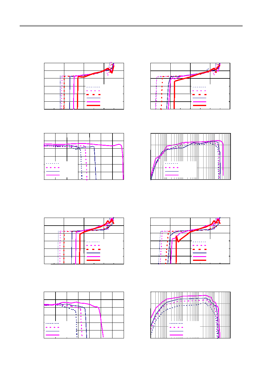
2. S-8351A50MC (built-in, V
OUT
=
=
=
= 5 V)
2-1 CDRH6D28-101 (100
ĶH), Ta = 25įC
2-2 CDRH125-221 (220
ĶH), Ta = 25įC
2.8
2.9
3.0
3.1
(d) Efficiency vs. Output current
(c) Output current vs. Output voltage
Output current
I
OUT
[mA]
O
u
tput v
o
lt
age V
OU
T
[V]
100
150
200
50
0
3.2
2.6
2.7
250
50
60
70
80
E
ffi
c
i
e
n
c
y
[%]
Output current
I
OUT
[mA]
1
10
100
1000
0.1
0.01
90
V
IN
= 1.0 V
V
IN
= 1.5 V
V
IN
= 1.8 V
V
IN
= 2.0 V
V
IN
= 2.5 V
V
IN
= 1.0 V
V
IN
= 1.5 V
V
IN
= 1.8 V
V
IN
= 2.0 V
V
IN
= 2.5 V
4.8
4.9
5.0
5.1
(b) Input voltage vs. Output voltage
(input voltage stepped down)
(a) Input voltage vs. Output voltage
(input voltage stepped up)
Input voltage V
IN
[V]
O
u
tput v
o
lt
age V
OUT
[V]
2
3
5
1
0
I
OUT
= 0.1 mA
I
OUT
= 1 mA
I
OUT
= 10 mA
I
OUT
= 50 mA
I
OUT
= 100 mA
I
OUT
= 150 mA
5.2
4.6
4.7
4.8
4.9
5.0
5.1
Input voltage V
IN
[V]
O
u
tput v
o
lt
age V
OUT
[V]
5.2
4.6
4.7
4
6
I
OUT
= 0.1 mA
I
OUT
= 1 mA
I
OUT
= 10 mA
I
OUT
= 50 mA
I
OUT
= 100 mA
I
OUT
= 150 mA
2
3
5
1
0
4
6
4.8
4.9
5.0
5.1
(d) Efficiency vs. Output current
(c) Output current vs. Output voltage
Output current
I
OUT
[mA]
O
u
tput v
o
lt
age V
OUT
[V]
100
150
200
50
0
V
IN
= 1.5 V
V
IN
= 2.0 V
V
IN
= 3.0 V
5.2
4.6
4.7
250
60
70
80
90
E
ffi
c
i
e
n
c
y
[%]
Output current
I
OUT
[mA]
1
10
100
1000
0.1
0.01
100
V
IN
= 1.0 V
V
IN
= 1.5 V
V
IN
= 2.0 V
V
IN
= 3.0 V
V
IN
= 4.0 V
4.8
4.9
5.0
5.1
(b) Input voltage vs. Output voltage
(input voltage stepped down)
(a) Input voltage vs. Output voltage
(input voltage stepped up)
Input voltage
V
IN
[V]
O
u
tput v
o
lt
age V
OUT
[V]
2
3
5
1
0
I
OUT
= 0.1 mA
I
OUT
= 1 mA
I
OUT
= 10 mA
I
OUT
= 50 mA
I
OUT
= 100 mA
I
OUT
= 150 mA
5.2
4.6
4.7
4.8
4.9
5.0
5.1
Input voltage
V
IN
[V]
O
u
tput v
o
lt
age V
OUT
[V]
5.2
4.6
4.7
4
6
I
OUT
= 0.1 mA
I
OUT
= 1 mA
I
OUT
= 10 mA
I
OUT
= 50 mA
I
OUT
= 100 mA
I
OUT
= 150 mA
2
3
5
1
0
4
6
SMALL PACKAGE PFM CONTROL STEP-UP SWITCHING REGULATOR
S-8351/52 Series
Rev.1.0
_10
Seiko Instruments Inc.
28
2-3 CXLP120-470 (47
ĶH), Ta = 25įC
4.8
4.9
5.0
5.1
(d) Efficiency vs. Output current
(c) Output current vs. Output voltage
Output current
I
OUT
[mA]
O
u
tput v
o
lt
age V
OU
T
[V]
100
150
200
50
0
V
IN
= 1.5 V
V
IN
= 2.0 V
V
IN
= 3.0 V
5.2
4.6
4.7
250
60
70
80
90
E
ffi
c
i
e
n
c
y
[%]
Output current
I
OUT
[mA]
1
10
100
1000
0.1
0.01
100
V
IN
= 1.0 V
V
IN
= 1.5 V
V
IN
= 2.0 V
V
IN
= 3.0 V
V
IN
= 4.0 V
4.8
4.9
5.0
5.1
(b) Input voltage vs. Output voltage
(input voltage stepped down)
(a) Input voltage vs. Output voltage
(input voltage stepped up)
Input voltage V
IN
[V]
O
u
tput v
o
lt
age V
OUT
[V]
2
3
5
1
0
I
OUT
= 0.1 mA
I
OUT
= 1 mA
I
OUT
= 10 mA
I
OUT
= 50 mA
I
OUT
= 100 mA
I
OUT
= 150 mA
5.2
4.6
4.7
4.8
4.9
5.0
5.1
Input voltage V
IN
[V]
O
u
tput v
o
lt
age V
OUT
[V]
5.2
4.6
4.7
4
6
I
OUT
= 0.1 mA
I
OUT
= 1 mA
I
OUT
= 10 mA
I
OUT
= 50 mA
I
OUT
= 100 mA
I
OUT
= 150 mA
2
3
5
1
0
4
6
4.8
4.9
5.0
5.1
(d) Efficiency vs. Output current
(c) Output current vs. Output voltage
Output current
I
OUT
[mA]
O
u
t
put
vol
t
ag
e V
OU
T
[V]
100
150
200
50
0
V
IN
= 1.5 V
V
IN
= 2.0 V
V
IN
= 3.0 V
5.2
4.6
4.7
250
50
60
70
80
Ef
f
i
c
i
enc
y
[%
]
Output current
I
OUT
[mA]
1
10
100
1000
0.1
0.01
90
V
IN
= 1.0 V
V
IN
= 1.5 V
V
IN
= 2.0 V
V
IN
= 3.0 V
V
IN
= 4.0 V
SMALL PACKAGE PFM CONTROL STEP-UP SWITCHING REGULATOR
Rev.1.0
_10
S-8351/52 Series
Seiko Instruments Inc.
29
3. S-8352A30MC (external, V
OUT
=
=
=
= 3 V)
3-1 CDRH6D28-220 (22
ĶH), Ta = 25įC
3-2 CDRH6D28-101 (100
ĶH), Ta = 25įC
2.8
2.9
3.0
3.1
(d) Efficiency vs. Output current
(c) Output current vs. Output voltage
Output current
I
OUT
[mA]
O
u
tput v
o
lt
age V
OU
T
[V]
100
150
200
50
0
3.2
2.6
2.7
250
50
60
70
80
E
ffi
c
i
e
n
c
y
[%]
Output current
I
OUT
[mA]
1
10
100
1000
0.1
0.01
90
300
350
V
IN
= 1.8 V
V
IN
= 2.0 V
V
IN
= 2.5 V
V
IN
= 1.5 V
V
IN
= 1.8 V
V
IN
= 2.0 V
V
IN
= 2.5 V
V
IN
= 1.5 V
2.8
2.9
3.0
3.1
(b) Input voltage vs. Output voltage
(input voltage stepped down)
(a) Input voltage vs. Output voltage
(input voltage stepped up)
Input voltage V
IN
[V]
O
u
tput v
o
lt
age V
OUT
[V]
2
3
4
1
0
3.2
2.6
2.7
2.8
2.9
3.0
3.1
Input voltage V
IN
[V]
O
u
tput v
o
lt
age V
OUT
[V]
2
3
4
1
0
3.2
2.6
2.7
I
OUT
= 0.1 mA
I
OUT
= 1 mA
I
OUT
= 10 mA
I
OUT
= 50 mA
I
OUT
= 100 mA
I
OUT
= 150 mA
I
OUT
= 0.1 mA
I
OUT
= 1 mA
I
OUT
= 10 mA
I
OUT
= 50 mA
I
OUT
= 100 mA
I
OUT
= 150 mA
2.8
2.9
3.0
3.1
(b) Input voltage vs. Output voltage
(input voltage stepped down)
(a) Input voltage vs. Output voltage
(input voltage stepped up)
Input voltage V
IN
[V]
O
u
tput v
o
lt
age V
OUT
[V]
2
3
4
1
0
I
OUT
= 0.1 mA
I
OUT
= 1 mA
I
OUT
= 10 mA
I
OUT
= 50 mA
I
OUT
= 100 mA
I
OUT
= 150 mA
3.2
2.6
2.7
2.8
2.9
3.0
3.1
Input voltage V
IN
[V]
O
u
tput v
o
lt
age V
OUT
[V]
2
3
4
1
0
I
OUT
= 0.1 mA
I
OUT
= 1 mA
I
OUT
= 10 mA
I
OUT
= 50 mA
I
OUT
= 100 mA
I
OUT
= 150 mA
3.2
2.6
2.7
2.8
2.9
3.0
3.1
(d) Efficiency vs. Output current
(c) Output current vs. Output voltage
Output current
I
OUT
[mA]
O
u
tput v
o
lt
age V
OU
T
[V]
3.2
2.6
2.7
50
60
70
80
E
ffi
c
i
e
n
c
y
[%]
Output current
I
OUT
[mA]
1
10
100
1000
0.1
0.01
90
100
150
200
50
0
250
300
350
V
IN
= 1.8 V
V
IN
= 2.0 V
V
IN
= 2.5 V
V
IN
= 1.5 V
V
IN
= 1.8 V
V
IN
= 2.0 V
V
IN
= 2.5 V
V
IN
= 1.5 V

SMALL PACKAGE PFM CONTROL STEP-UP SWITCHING REGULATOR
S-8351/52 Series
Rev.1.0
_10
Seiko Instruments Inc.
30
3-3 CXLP120-470 (47
ĶH), Ta = 25įC
4. S-8352A50MC (external, V
OUT
=
=
=
= 5 V)
4-1 CDRH6D28-220 (22
ĶH), Ta = 25įC
2.8
2.9
3.0
3.1
(b) Input voltage vs. Output voltage
(input voltage stepped down)
(a) Input voltage vs. Output voltage
(input voltage stepped up)
Input voltage V
IN
[V]
O
u
tput v
o
lt
age V
OUT
[V]
2
3
4
1
0
I
OUT
= 0.1 mA
I
OUT
= 1 mA
I
OUT
= 10 mA
I
OUT
= 50 mA
I
OUT
= 100 mA
I
OUT
= 150 mA
3.2
2.6
2.7
2.8
2.9
3.0
3.1
Input voltage V
IN
[V]
O
u
tput v
o
lt
age V
OUT
[V]
2
3
4
1
0
I
OUT
= 0.1 mA
I
OUT
= 1 mA
I
OUT
= 10 mA
I
OUT
= 50 mA
I
OUT
= 100 mA
I
OUT
= 150 mA
3.2
2.6
2.7
2.8
2.9
3.0
3.1
(d) Efficiency vs. Output current
(c) Output current vs. Output voltage
Output current
I
OUT
[mA]
O
u
tput v
o
lt
age V
OU
T
[V]
3.2
2.6
2.7
50
60
70
80
E
ffi
c
i
e
n
c
y
[%]
Output current
I
OUT
[mA]
1
10
100
1000
0.1
0.01
90
100
150
200
50
0
250
300
350
V
IN
= 1.8 V
V
IN
= 2.0 V
V
IN
= 2.5 V
V
IN
= 1.5 V
V
IN
= 1.8 V
V
IN
= 2.0 V
V
IN
= 2.5 V
V
IN
= 1.5 V
4.8
4.9
5.0
5.1
(d) Efficiency vs. Output current
(c) Output current vs. Output voltage
Output current
I
OUT
[mA]
O
u
tput v
o
lt
age V
OU
T
[V]
100
200
300
50
0
5.2
4.6
4.7
400
50
60
70
80
E
ffi
c
i
e
n
c
y
[%]
Output current
I
OUT
[mA]
1
10
100
1000
0.1
0.01
90
V
IN
= 2.0 V
V
IN
= 3.0 V
V
IN
= 4.0 V
150
250
350
450
V
IN
= 1.5 V
V
IN
= 2.0 V
V
IN
= 3.0 V
V
IN
= 4.0 V
4.8
4.9
5.0
5.1
(b) Input voltage vs. Output voltage
(input voltage stepped down)
(a) Input voltage vs. Output voltage
(input voltage stepped up)
Input voltage V
IN
[V]
O
u
tput v
o
lt
age V
OUT
[V]
2
3
5
1
0
I
OUT
= 0.1 mA
I
OUT
= 1 mA
I
OUT
= 10 mA
I
OUT
= 50 mA
I
OUT
= 100 mA
I
OUT
= 150 mA
5.2
4.6
4.7
4.8
4.9
5.0
5.1
Input voltage V
IN
[V]
O
u
tput v
o
lt
age V
OUT
[V]
5.2
4.6
4.7
4
6
I
OUT
= 0.1 mA
I
OUT
= 1 mA
I
OUT
= 10 mA
I
OUT
= 50 mA
I
OUT
= 100 mA
I
OUT
= 150 mA
2
3
5
1
0
4
6
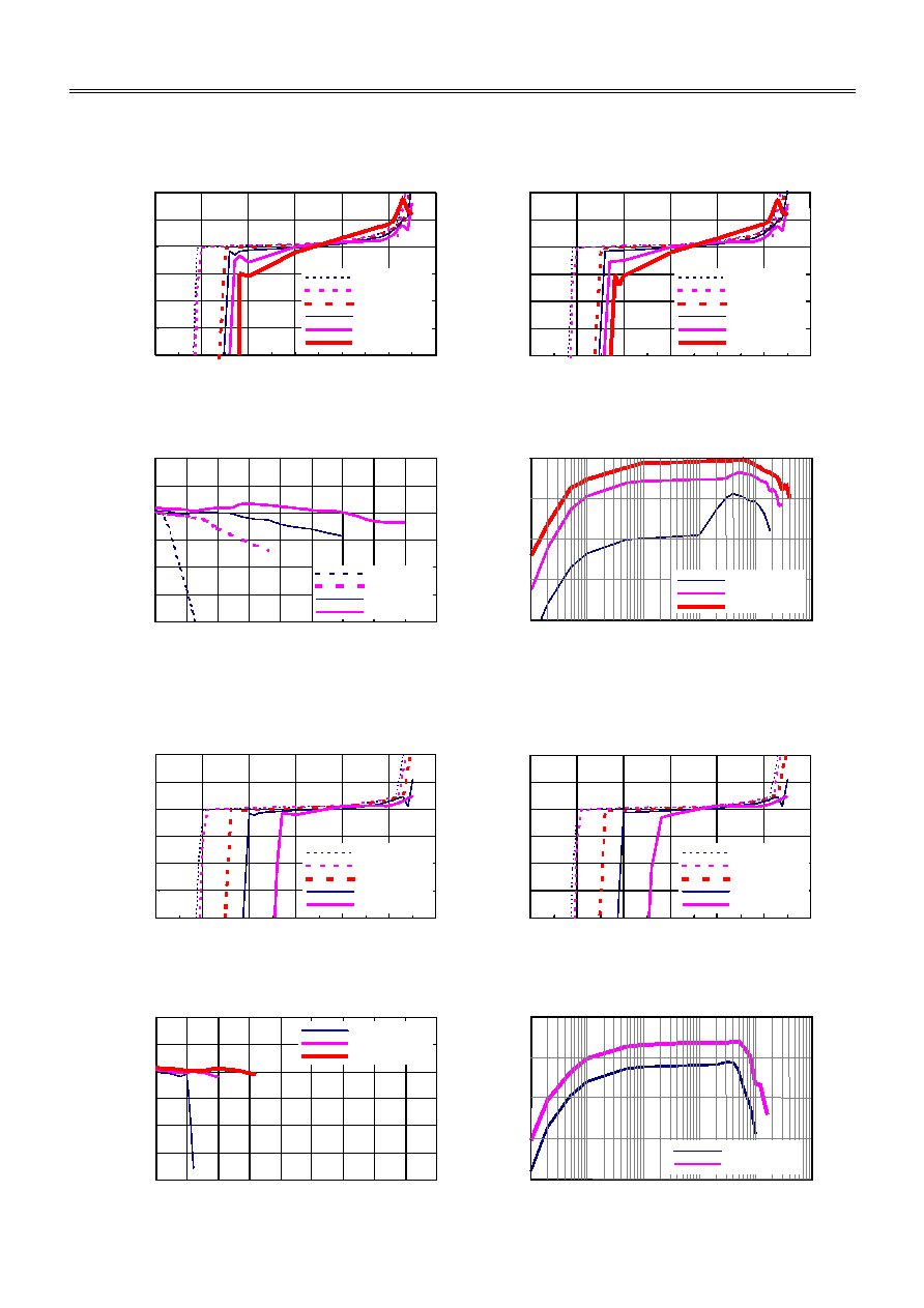
SMALL PACKAGE PFM CONTROL STEP-UP SWITCHING REGULATOR
Rev.1.0
_10
S-8351/52 Series
Seiko Instruments Inc.
31
4-2 CDRH6D28-101 (100
ĶH), Ta = 25įC
4-3 CXLP120-101 (100
ĶH), Ta = 25įC
4.8
4.9
5.0
5.1
(d) Efficiency vs. Output current
(c) Output current vs. Output voltage
Output current
I
OUT
[mA]
O
u
tput v
o
lt
age V
OU
T
[V]
5.2
4.6
4.7
50
60
70
80
E
ffi
c
i
e
n
c
y
[%]
Output current
I
OUT
[mA]
1
10
100
1000
0.1
0.01
90
100
200
300
50
0
400
150
250
350
450
V
IN
= 1.5 V
V
IN
= 2.0 V
V
IN
= 3.0 V
V
IN
= 4.0 V
V
IN
= 2.0 V
V
IN
= 3.0 V
V
IN
= 4.0 V
4.8
4.9
5.0
5.1
(b) Input voltage vs. Output voltage
(input voltage stepped down)
(a) Input voltage vs. Output voltage
(input voltage stepped up)
Input voltage V
IN
[V]
O
u
tput v
o
lt
age V
OUT
[V]
2
3
5
1
0
5.2
4.6
4.7
4.8
4.9
5.0
5.1
Input voltage V
IN
[V]
O
u
tput v
o
lt
age V
OUT
[V]
5.2
4.6
4.7
4
6
I
OUT
= 0.1 mA
I
OUT
= 1 mA
I
OUT
= 10 mA
I
OUT
= 50 mA
I
OUT
= 100 mA
I
OUT
= 150 mA
2
3
5
1
0
4
6
I
OUT
= 0.1 mA
I
OUT
= 1 mA
I
OUT
= 10 mA
I
OUT
= 50 mA
I
OUT
= 100 mA
I
OUT
= 150 mA
4.8
4.9
5.0
5.1
(b) Input voltage vs. Output voltage
(input voltage stepped down)
(a) Input voltage vs. Output voltage
(input voltage stepped up)
Input voltage V
IN
[V]
O
u
tput v
o
lt
age V
OUT
[V]
2
3
5
1
0
I
OUT
= 0.1 mA
I
OUT
= 1 mA
I
OUT
= 10 mA
I
OUT
= 50 mA
I
OUT
= 100 mA
5.2
4.6
4.7
4.8
4.9
5.0
5.1
Input voltage V
IN
[V]
O
u
tput v
o
lt
age V
OUT
[V]
5.2
4.6
4.7
4
6
2
3
5
1
0
4
6
I
OUT
= 0.1 mA
I
OUT
= 1 mA
I
OUT
= 10 mA
I
OUT
= 50 mA
I
OUT
= 100 mA
4.8
4.9
5.0
5.1
(d) Efficiency vs. Output current
(c) Output current vs. Output voltage
Output current
I
OUT
[mA]
O
u
tput v
o
lt
age V
OU
T
[V]
V
IN
= 2.0 V
V
IN
= 3.0 V
V
IN
= 4.0 V
5.2
4.6
4.7
50
60
70
80
E
ffi
c
i
e
n
c
y
[%]
Output current
I
OUT
[mA]
1
10
100
1000
0.1
0.01
90
V
IN
= 3.0 V
V
IN
= 4.0 V
100
200
300
50
0
400
150
250
350
450
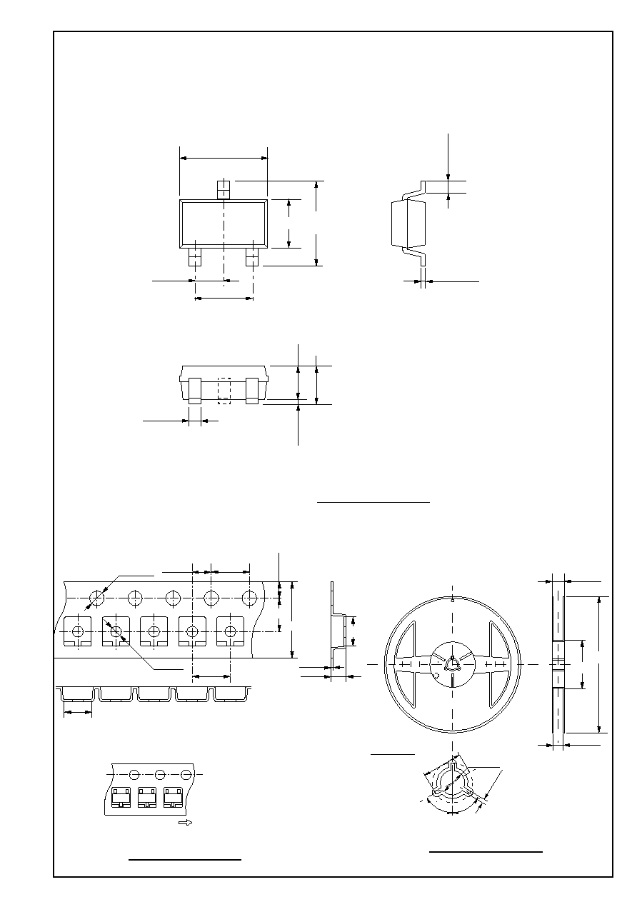
2.9Ī0.2
0.95Ī0.1
1.9Ī0.2
+0.1
-0.05
0.16
0.4Ī0.1
0.25
+0.2
-0.6
2.8
0
0.1
1
2
3
1.5
1.3max.
1.1Ī0.1
T2
1.6Ī0.1
0.25Ī0.05
4.0Ī0.1
2.0Ī0.1
4.0Ī0.1
1.5
+0.1
-0.05
1.1Ī0.1
2.85Ī0.2
Feed direction
1.75Ī0.1
3.5Ī0.1
8.0Ī0.2
3.05Ī0.2
No.:MP003-A-C-SD-1.0
21Ī0.5
2Ī0.2
(60į)
(60į)
Ý13Ī0.2
12.5max.
9.0Ī0.3
Winding core
Ý60
+1
-0
Ý180
+0
-3
n SOT-23-3
MP003-A 990531
No.:MP003-A-P-SD-1.0
No.:MP003-A-R-SD-1.0
Unit:mm
lDimensions
lTaping Specifications
lReel Specifications
1 reel holds 3000 ICs.
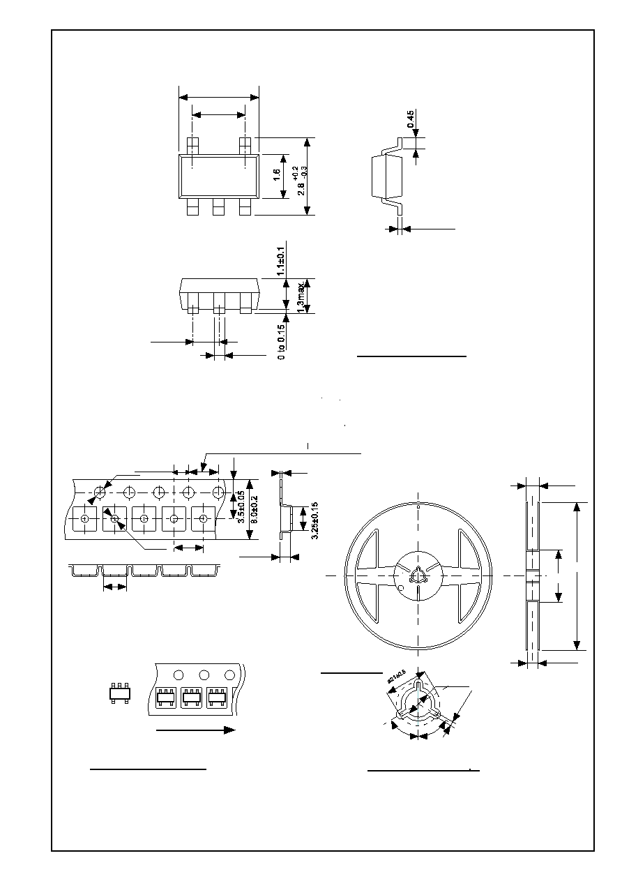
l Reel Specifications
l Tape Specifications
l Dimensions
n SOT-23-5
MP005-A
010907
Unit : mm
2.9Ī0.2
1.9Ī0.2
0.95Ī0.1
0.4Ī0.1
0.16
+0.1
-0.06
1
2
3
4
5
No. MP005-A-P-SD-1.1
12.5max.
9.0Ī0.3
Ý13Ī0.2
(60į)
(60į)
+0
-3
Ý180
Ý60 +1
-0
2Ī0.2
No. MP005-A-R-SD-1 0
3000 pcs./reel
Winding core
Ý1.5
+0.1
-0
2.0Ī0.05
4.0Ī0.1(10-pitches tota :40.0Ī0.2)
Ý1.0
+0.2
-0
4.0Ī0.1
1.4Ī0.2
0.25Ī0.1
3.2Ī0.2
T 2( T F )
1
2
3
4 5
Feed direction
1.75Ī0.1
No. : MP005-A-C-SD-2.0
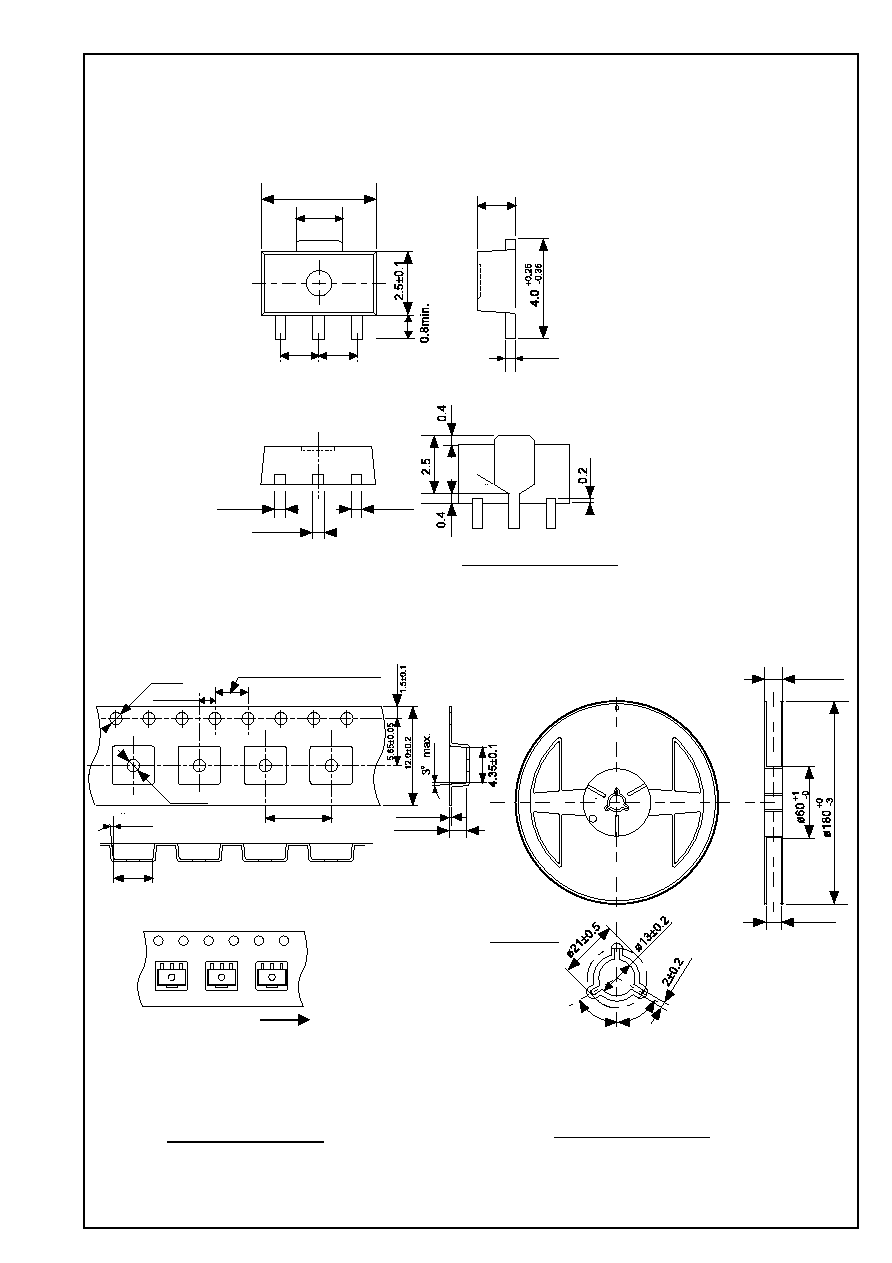
Winding core
No. UP003-A-R-SD-1.0
1 reel holds 1000 ICs.
13.0Ī0.3
16.5max.
(60į)
(60į)
No. UP003-A-C-SD-1.0
No. UP003-A-P-SD-1.0
0.4Ī0.05
1.5Ī0.1
4.5Ī0.1
1.6Ī0.2
1.5Ī0.11.5Ī0.1
0.45Ī0.1
0.4Ī0.1
0.4Ī0.1
45
3
1
2
n SOT-89-3
Unit:mm
lDimensions
lTaping Specifications
lReel Specifications
UP003-A
Rev.1.0
020109
4.0Ī0.1(10 pitches:40.0Ī0.2)
T2
Feed direction
2.0Ī0.1
0.3Ī0.05
8.0Ī0.1
Ý1.5
+0.1
-0
2.0Ī0.05
Ý1.5
+0.1
-0
4.75Ī0.1
5 max.

∑
The information described herein is subject to change without notice.
∑
Seiko Instruments Inc. is not responsible for any problems caused by circuits or diagrams described herein
whose related industrial properties, patents, or other rights belong to third parties. The application circuit
examples explain typical applications of the products, and do not guarantee the success of any specific
mass-production design.
∑
When the products described herein are regulated products subject to the Wassenaar Arrangement or other
agreements, they may not be exported without authorization from the appropriate governmental authority.
∑
Use of the information described herein for other purposes and/or reproduction or copying without the
express permission of Seiko Instruments Inc. is strictly prohibited.
∑
The products described herein cannot be used as part of any device or equipment affecting the human
body, such as exercise equipment, medical equipment, security systems, gas equipment, or any apparatus
installed in airplanes and other vehicles, without prior written permission of Seiko Instruments Inc.
∑
Although Seiko Instruments Inc. exerts the greatest possible effort to ensure high quality and reliability, the
failure or malfunction of semiconductor products may occur. The user of these products should therefore
give thorough consideration to safety design, including redundancy, fire-prevention measures, and
malfunction prevention, to prevent any accidents, fires, or community damage that may ensue.