Document Outline
- S-8353/8354 Series
- Cover
- Features
- Applications
- Packages
- Block Diagrams
- Product Name Structure
- Pin Configurations
- Absolute Maximum Ratings
- Electrical Characteristics
- Test Circuits
- Operation
- External Parts Selection for DC-DC Converter
- Standard Circuits
- Power Dissipation of Package
- Precautions
- Application Circuits
- Examples of Major Temperature Characteristics
- Examples of Major Power Supply Dependence Characteristics
- Output Waveforms
- Examples of Transient Response Characteristics
- Reference Data
- Package drawings

Rev.1.2
_00
ULTRA-SMALL PACKAGE PWM CONTROL, PWM/PFM
SWITCHING CONTROL STEP-UP SWITCHING REGULATOR
S-8353/8354 Series
Seiko Instruments Inc.
1
The S-8353/8354 Series is a CMOS step-up switching
regulator which mainly consists of a reference voltage
source, an oscillation circuit, a power MOS FET, an
error amplifier, a phase compensation circuit, a PWM
controller (S-8353 Series) and a PWM/PFM switching
controller (S-8354 Series).
Simply attaching a coil, capacitor, and diode externally
can configure the step-up switching regulator. In
addition to the above features, the small package and
low power consumption of this series make it ideal for
portable device applications requiring high efficiency.
The S-8353 Series realizes low ripple, high efficiency,
and excellent transient characteristics due to its PWM
controller, which can vary the duty ratio linearly from
0 % to 83 % (from 0 % to 78 % for 250 kHz models),
optimally-designed error amplifier, and phase
compensation circuits.
The S-8354 Series features a PWM/PFM switching
controller that can switch the operation to a PFM
controller with a duty ratio is 15 % under a light load to
prevent a decline in the efficiency due to the IC
operating current.
Features
∑ Low voltage operation:
Start-up is guaranteed from 0.9 V (I
OUT
=1 mA)
∑ Low current consumption:
During operation: 18.7
µA (3.3 V, 50 kHz, typ.)
During shutdown: 0.5
µA (max.)
∑ Duty ratio:
Built-in PWM/PFM switching control circuit (S-8354 Series)
15 % to 83 % (30 kHz and 50 kHz models), 15 % to 78 % (250 kHz models)
∑ External parts:
Coil, capacitor, and diode
∑ Output voltage:
Can be set in 0.1 V steps between 1.5 and 6.5 V (for V
DD
/V
OUT
separate
types) or 2.0 and 6.5 V (for other than V
DD
/V
OUT
separate types). Accuracy
of
±2.4%.
∑ Oscillation frequency:
30 kHz, 50 kHz, and 250 kHz
∑ Soft start function:
6 ms (50 kHz, typ.)
Applications
∑ Power supplies for portable equipment such as digital cameras, electronic notebooks, and PDAs
∑ Power supplies for audio equipment such as portable CD/MD players
∑ Constant voltage power supplies for cameras, video equipment, and communications equipment
∑ Power supplies for microcomputers
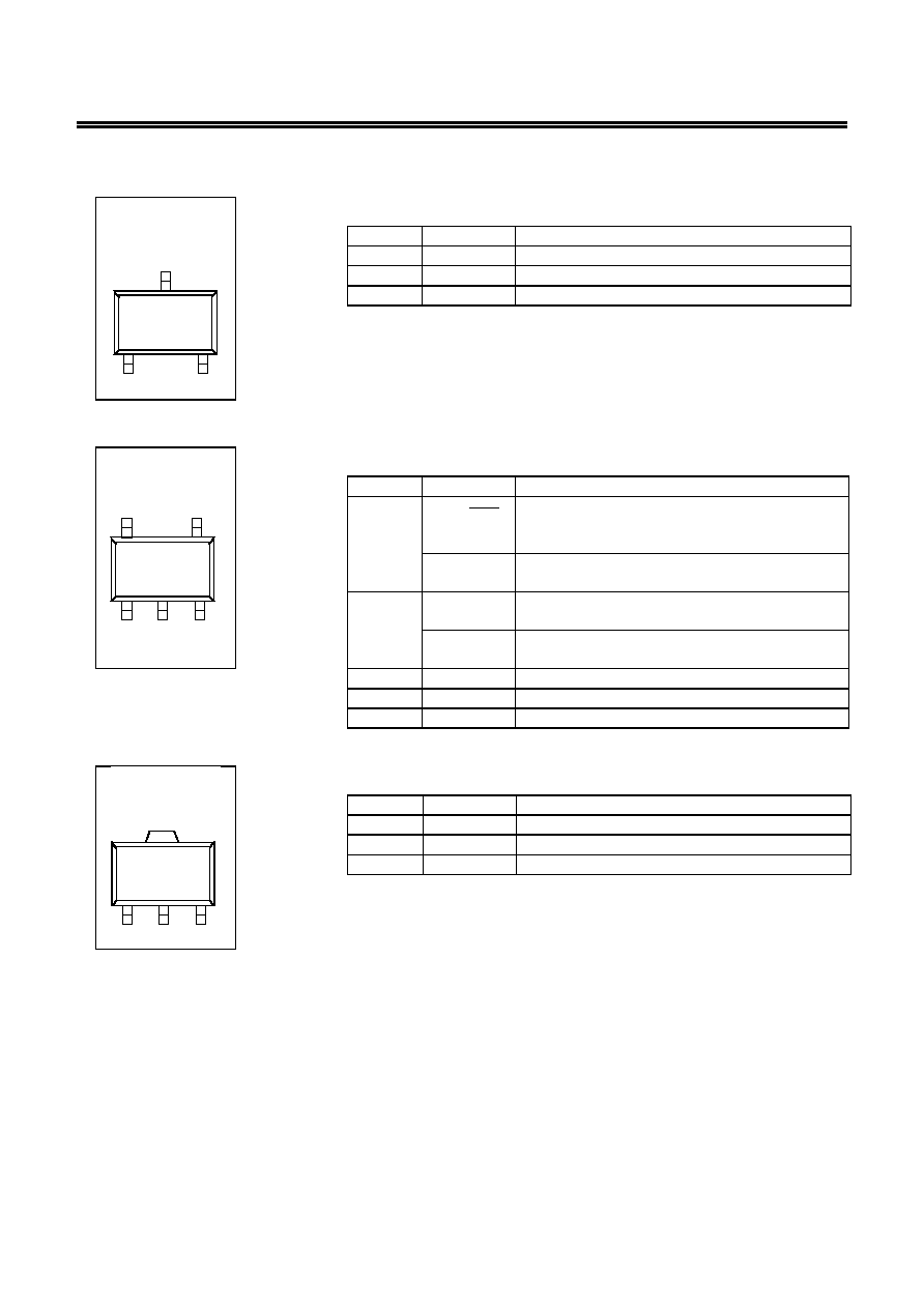
Packages
Package name
Drawing code
Package Tape
Reel
SOT-23-3 MP003-A MP003-A MP003-A
SOT-23-5 MP005-A MP005-A MP005-A
SOT-89-3 UP003-A UP003-A UP003-A
ULTRA-SMALL PACKAGE PWM CONTROL, PWM/PFM SWITCHING CONTROL STEP-UP SWITCHING REGULATOR
S-8353/8354 Series
Rev.1.2
_00
2
Seiko Instruments Inc.
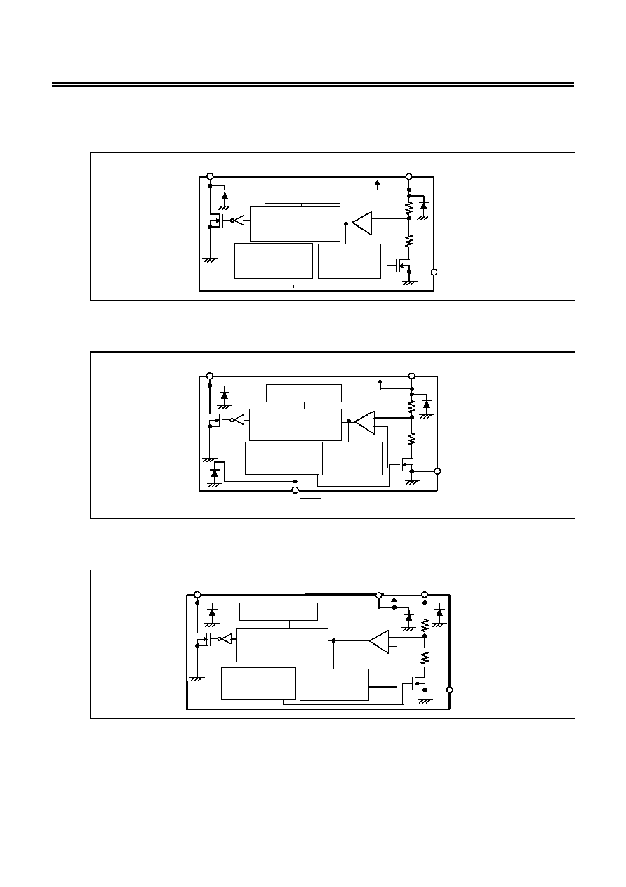
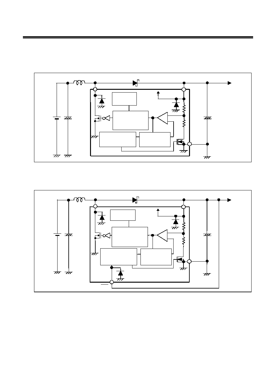
Block Diagrams
1. A, C, H type (Without Shutdown Function)
VOUT
VSS
IC internal
power supply
-
+
CONT
Oscillation circuit
PWM control,
PWM/PFM switching
control circuit
Phase
compensation
circuit
Soft start built-in
reference power
supply
Figure 1
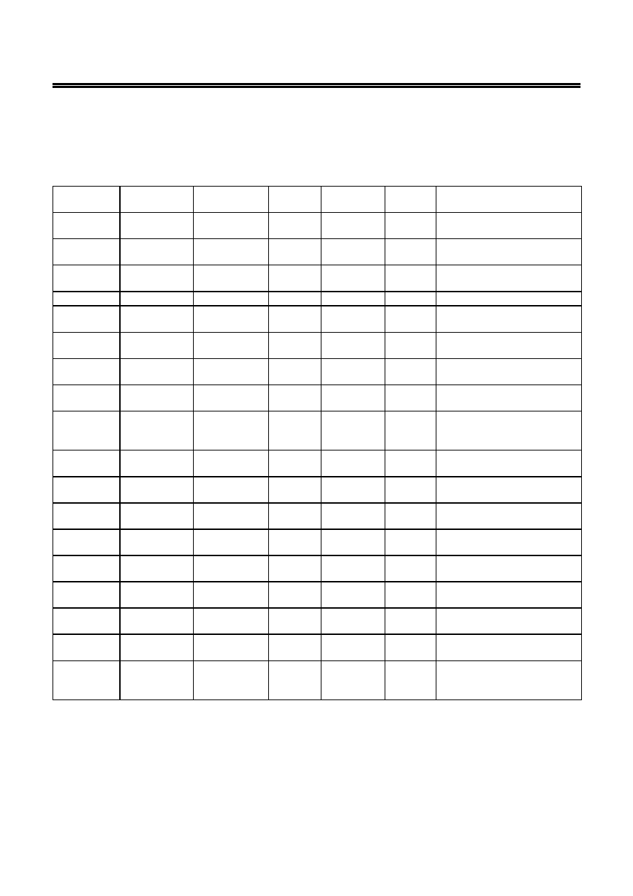
2. A, H type (With Shutdown Function)
VOUT
VSS
IC internal
power supply
-
+
OFF
/
ON
CONT
Oscillation circuit
PWM control,
PWM/PFM switching
control circuit
Soft start built-in
reference power
supply
Phase
compensation
circuit
Figure 2
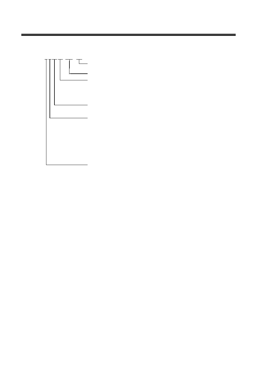
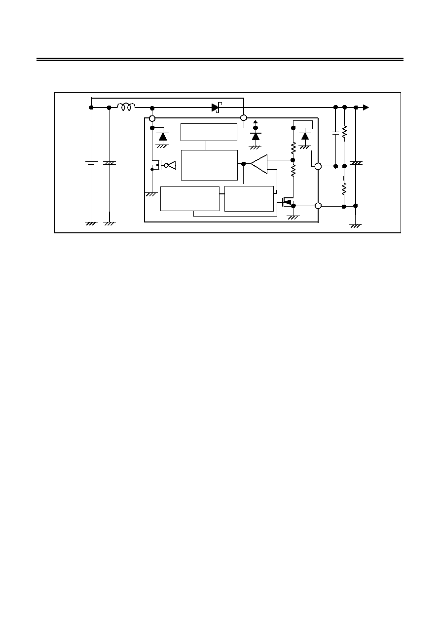
3. D, J type
VDD
CONT
-
+
VOUT
VSS
Oscillation circuit
PWM control,
PWM/PFM switching
control circuit
Soft start built-in
reference power
supply
Phase
compensation
circuit
IC internal
power supply
Figure 3
ULTRA-SMALL PACKAGE PWM CONTROL, PWM/PFM SWITCHING CONTROL STEP-UP SWITCHING REGULATOR
Rev.1.2
_00
S-8353/8354 Series
Seiko Instruments Inc.
3
Product Name Structure
1. Function List
Table 1
Product name Control system
Switching
frequency [kHz]
Shutdown
function
V
DD
/V
OUT
separate type
Package Application
S-8353AxxMC PWM
50
Yes
SOT-23-5
Application requiring shutdown
function
S-8353AxxMA PWM
50
SOT-23-3
Application not requiring shutdown
function
S-8353AxxUA PWM
50
SOT-89-3
Application not requiring shutdown
function
S-8353CxxMA PWM
30
SOT-23-3 For pager
S-8353DxxMC PWM
50
Yes SOT-23-5
Application in which output voltage
is adjusted by external resistance
S-8353HxxMC PWM
250
Yes
SOT-23-5
Application requiring shutdown
function and thin coil
S-8353HxxMA PWM
250
SOT-23-3
Application not requiring shutdown
function and requiring thin coil
S-8353HxxUA PWM
250
SOT-89-3
Application not requiring shutdown
function and requiring thin coil
S-8353JxxMC PWM
250
Yes SOT-23-5
Application in which output voltage
is adjusted by external resistance
and that requires thin coil
S-8354AxxMC
PWM/PFM
switching
50 Yes
SOT-23-5
Application requiring shutdown
function
S-8354AxxMA
PWM/PFM
switching
50
SOT-23-3
Application not requiring shutdown
function
S-8354AxxUA
PWM/PFM
switching
50
SOT-89-3
Application not requiring shutdown
function
S-8354CxxMA
PWM/PFM
switching
30
SOT-23-3 For pager
S-8354DxxMC
PWM/PFM
switching
50
Yes SOT-23-5
Application in which output voltage
is adjusted by external resistance
S-8354HxxMC
PWM/PFM
switching
250 Yes
SOT-23-5
Application requiring shutdown
function and thin coil
S-8354HxxMA
PWM/PFM
switching
250
SOT-23-3
Application not requiring shutdown
function and requiring thin coil
S-8354HxxUA
PWM/PFM
switching
250
SOT-89-3
Application not requiring shutdown
function and requiring thin coil
S-8354JxxMC
PWM/PFM
switching
250
Yes SOT-23-5
Application in which output voltage
is adjusted by external resistance
and that requires thin coil
ULTRA-SMALL PACKAGE PWM CONTROL, PWM/PFM SWITCHING CONTROL STEP-UP SWITCHING REGULATOR
S-8353/8354 Series
Rev.1.2
_00
4
Seiko Instruments Inc.
2. Product Name
S-835 x x xx xx - xxx - T2
IC direction in tape specifications
*1
Product code
*2
Package code
MA: SOT-23-3
MC: SOT-23-5
UA: SOT-89-3
Output voltage
15 to 65
(Ex. When the output voltage is 1.5 V, it is expressed as 15.)
Product type
A: Normal products (SOT23-3, SOT-89-3),
f
osc
=50 kHz
or With shutdown function products (SOT-23-5), f
osc
=50 kHz
C: Normal products
f
osc
=30 kHz
D: V
DD
/V
OUT
separate type,
f
osc
=50 kHz
H: Normal products (SOT23-3, SOT-89-3),
f
osc
=250 kHz
or With shutdown function products (SOT-23-5), f
osc
=250 kHz
J: V
DD
/V
OUT
separate type,
f
osc
=250 kHz
Control system
3: PWM control
4: PWM/PFM control
*1. Refer to the taping specifications at the end of this book.
*2. Refer to the "3. Product Name List".
ULTRA-SMALL PACKAGE PWM CONTROL, PWM/PFM SWITCHING CONTROL STEP-UP SWITCHING REGULATOR
Rev.1.2
_00
S-8353/8354 Series
Seiko Instruments Inc.
5
3. Product Name List
3-1. S-8353 Series
Table 2
Output voltage S-8353AxxMC Series
S-8353AxxMA Series
S-8353AxxUA Series
S-8353CxxMA Series
2.0 V
S-8353A20MC-IQF-T2
2.5 V
S-8353A25MC-IQK-T2
2.7 V
S-8353A27MC-IQM-T2
2.8 V
S-8353A28MC-IQN-T2
3.0 V
S-8353A30MC-IQP-T2
S-8353A30MA-IQP-T2
S-8353C30MA-ISP-T2
3.3 V
S-8353A33MC-IQS-T2
S-8353A33MA-IQS-T2
S-8353A33UA-IQS-T2
3.8 V
S-8353A38MC-IQX-T2
5.0 V
S-8353A50MC-IRJ-T2
S-8353A50MA-IRJ-T2
S-8353A50UA-IRJ-T2
Remark Please contact the SII marketing department for products with an output voltage other than those
specified above.
Table 3
Output voltage S-8353DxxMC Series
S-8353HxxMC Series
S-8353JxxMC Series
2.0 V
S-8353D20MC-IUF-T2
S-8353J20MC-IYF-T2
2.5 V
S-8353J25MC-IYK-T2
3.0 V
S-8353D30MC-IUP-T2
S-8353H30MC-IWP-T2
3.1 V
S-8353H31MC-IWQ-T2
3.3 V
S-8353H33MC-IWS-T2
3.8 V
S-8353H38MC-IWX-T2
4.0 V
S-8353H40MC-IWZ-T2
4.5 V
S-8353H45MC-IXE-T2
5.0 V
S-8353D50MC-IVJ-T2
S-8353H50MC-IXJ-T2
S-8353J50MC-IZJ-T2
Remark Please contact the SII marketing department for products with an output voltage other than those
specified above.
3-2. S-8354 Series
Table 4
Output voltage S-8354AxxMC Series
S-8354AxxMA Series
S-8354AxxUA Series
S-8354DxxMC Series
2.0 V
S-8354D20MC-JUF-T2
2.7 V
S-8354A27MC-JQM-T2 S-8354A27MA-JQM-T2
3.0 V
S-8354A30MC-JQP-T2
S-8354A30MA-JQP-T2 S-8354A30UA-JQP-T2
3.3 V
S-8354A33MC-JQS-T2
S-8354A33MA-JQS-T2 S-8354A33UA-JQS-T2
4.0 V
S-8354A40MC-JQZ-T2
5.0 V
S-8354A50MC-JRJ-T2
S-8354A50MA-JRJ-T2
S-8354A50UA-JRJ-T2
Remark Please contact the SII marketing department for products with an output voltage other than those
specified above.
Table 5
Output voltage S-8354HxxMC Series
S-8354JxxMC Series
3.0 V
S-8354H30MC-JWP-T2
3.3 V
S-8354H33MC-JWS-T2
5.0 V
S-8354H50MC-JXJ-T2
S-8354J50MC-JZJ-T2
Remark Please contact the SII marketing department for products with an output voltage other than those
specified above.
ULTRA-SMALL PACKAGE PWM CONTROL, PWM/PFM SWITCHING CONTROL STEP-UP SWITCHING REGULATOR
S-8353/8354 Series
Rev.1.2
_00
6
Seiko Instruments Inc.
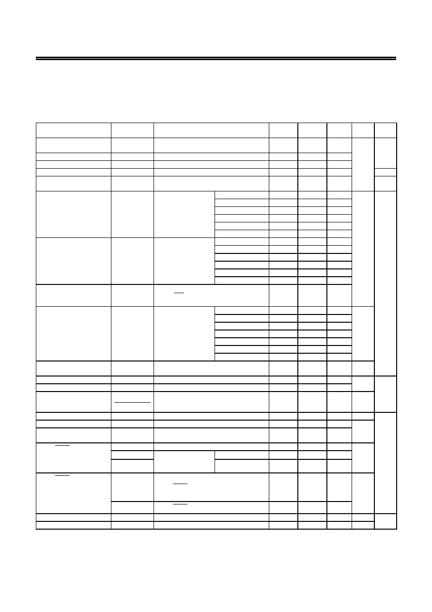
Pin Configurations
Table 6
Pin No.
Symbol
Pin description
1
VOUT
Output voltage and IC power supply pin
2
VSS
GND
pin
3
CONT
External inductor connection pin
1
3
2
SOT-23-3
Top view
Figure 4
Table 7
Pin No.
Symbol
Pin description
1
OFF
/
ON
(A, H type)
Shutdown pin
"H": Normal operation (Step-up operation)
"L": Stop step-up (Entire circuit stopped)
VOUT
(D, J type)
Output voltage pin
2
VOUT
(A, H type)
Output voltage and IC power supply pin
SOT-23-5
Top view
5
4
3
2
1
VDD
(D, J type)
IC power supply pin
3
NC
*1
No connection
Figure 5
4
VSS
GND
pin
5
CONT
External inductor connection pin
*1. The NC pin is electrically open.
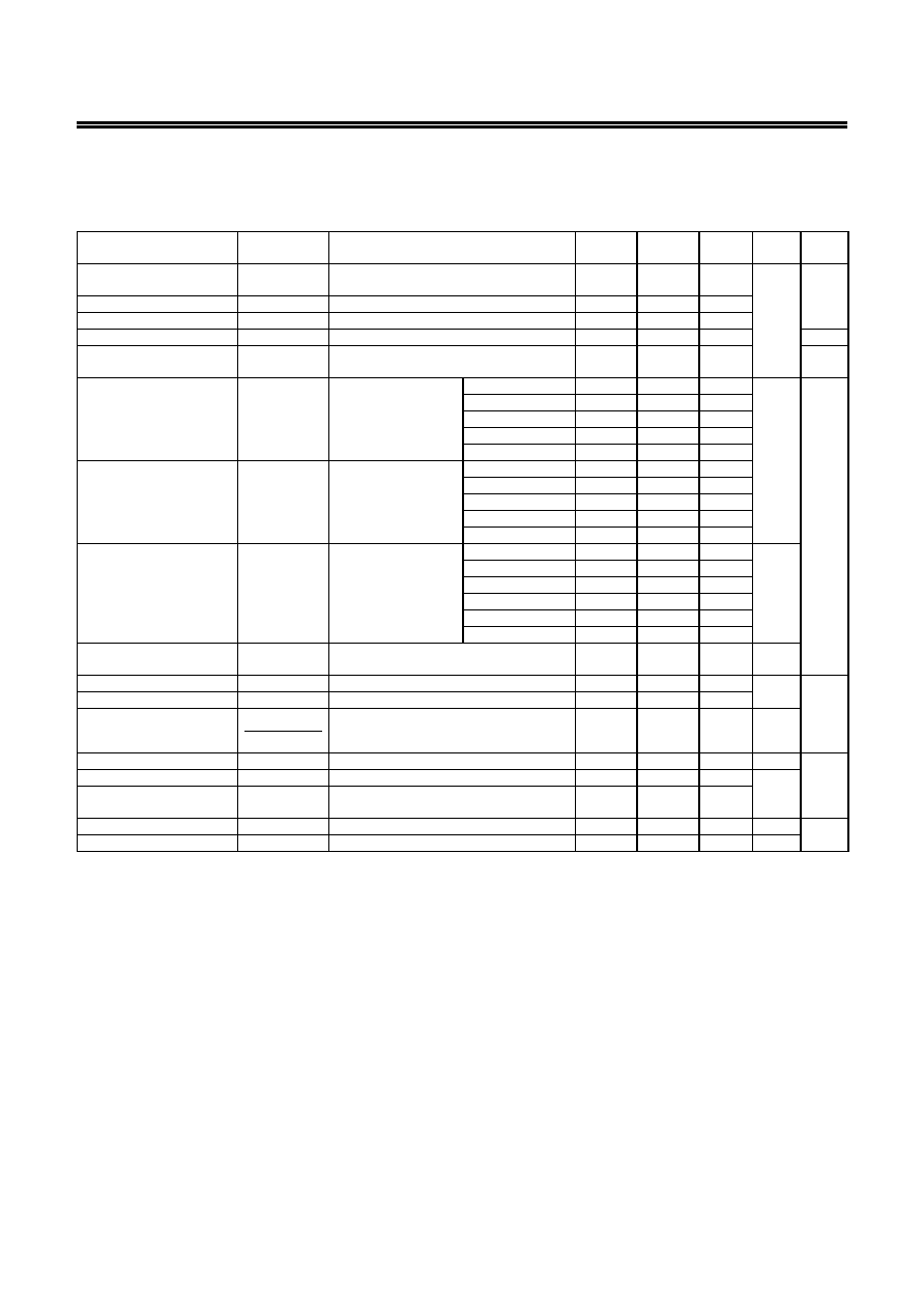
Table 8
Pin No.
Symbol
Pin description
1
VSS
GND
pin
2
VOUT
Output voltage and IC power supply pin
3
CONT
External inductor connection pin
SOT-89-3
Top view
3
2
1
Figure 6

ULTRA-SMALL PACKAGE PWM CONTROL, PWM/PFM SWITCHING CONTROL STEP-UP SWITCHING REGULATOR
Rev.1.2
_00
S-8353/8354 Series
Seiko Instruments Inc.
7
Absolute Maximum Ratings
Table 9
(Ta
=25∞C unless otherwise specified)
Item
Symbol
Absolute maximum rating
Unit
VOUT pin voltage
V
OUT
V
SS
-0.3 to V
SS
+12
V
OFF
/
ON
pin voltage
(S-835xAxxMC, S-835xHxxMC)
OFF
/
ON
V
V
SS
-0.3 to V
SS
+12
VDD pin voltage
(S-835xDxxMC, S-835xJxxMC)
V
DD
V
SS
-0.3 to V
SS
+12
CONT pin voltage
V
CONT
V
SS
-0.3 to V
SS
+12
CONT pin voltage
I
CONT
300
mA
Power dissipation
P
D
SOT-23-3
150
mW
SOT-23-5
250
SOT-89-3
500
Operating ambient temperature
Topr
-40 to +85
∞C
Storage ambient temperature
Tstg
-40 to +125
Caution The absolute maximum ratings are rated values exceeding which the product cloud suffer
physical damage. These values must therefore not be exceeded under any conditions.
ULTRA-SMALL PACKAGE PWM CONTROL, PWM/PFM SWITCHING CONTROL STEP-UP SWITCHING REGULATOR
S-8353/8354 Series
Rev.1.2
_00
8
Seiko Instruments Inc.
Electrical Characteristics
1. 50 kHz Product (A type, D type)
Table 10
(Ta
=25∞C unless otherwise specified)
Item Symbol
Condition
Min.
Typ.
Max.
Unit
Test
circuit
Output voltage
V
OUT
V
OUT(S)
◊0.976
V
OUT(S)
V
OUT(S)
◊1.024
V 2
Input voltage
V
IN
10
Operation start voltage
V
ST1
I
OUT
=1 mA
0.9
Oscillation start voltage
V
ST2
No external parts, Voltage applied to V
OUT
0.8 1
Operation holding voltage
V
HLD
I
OUT
=1 mA, Measured by decreasing V
IN
voltage gradually
0.7
2
Current consumption 1
I
SS1
V
OUT
=V
OUT(S)
◊0.95
S-835xx15 to 19
10.8 18.0
µA 1
S-835xx20 to 29
13.3 22.2
S-835xx30 to 39
18.7 31.1
S-835xx40 to 49
24.7 41.1
S-835xx50 to 59
31.0 51.6
S-835xx60 to 65
37.8 63.0
Current consumption 2
I
SS2
V
OUT
=V
OUT(S)
+ 0.5
S-835xx15 to 19
4.8 9.5
S-835xx20 to 29
5.0 9.9
S-835xx30 to 39
5.1 10.2
S-835xx40 to 49
5.3 10.6
S-835xx50 to 59
5.5 10.9
S-835xx60 to 65
5.7 11.3
Current consumption
during shutdown
(S-835xAxxMC Series)
I
SSS
OFF
/
ON
V
=0 V
0.5
Switching current
I
SW
V
CONT
=0.4 V
S-835xx15 to 19
80
128
mA
S-835xx20 to 24
103
165
S-835xx25 to 29
125
200
S-835xx30 to 39
144
231
S-835xx40 to 49
176
282
S-835xx50 to 59
200
320
S-835xx60 to 65
215
344
Switching transistor leak
current
I
SWQ
V
CONT
=V
OUT
=10 V
0.5 µA
Line regulation
V
OUT1
V
IN
=V
OUT(S)
◊0.4 to ◊0.6
30 60 mV 2
Load regulation
V
OUT2
I
OUT
=10 µA to V
OUT(S)
/ 250
◊1.25
30 60
Output voltage
temperature coefficient
OUT
OUT
V
Ta
V
∑
Ta
=-40∞C ~ +85∞C
±50
ppm/
∞C
Oscillation frequency
f
OSC
V
OUT
=V
OUT(S)
◊0.95 42.5
50
57.5
kHz
1
Maximum Duty ratio
MaxDuty
V
OUT
=V
OUT(S)
◊0.95 75
83
90
%
PWM/PFM switching duty
ratio (S-8354 Series)
PFMDuty V
IN
=V
OUT(S)
-0.1 V, No load
10
15
24
V
SH
Measured oscillation at CONT pin
0.75
V
V
SL1
When
V
OUT
1.5 V
0.3
OFF
/
ON
pin input
voltage
(S-835xAxxMC Series)
V
SL2
Judged the stop
oscillation at CONT
pin
When V
OUT
<1.5 V
0.2
OFF
/
ON
pin input
current
(S-835xAxxMC Series)
I
SH
OFF
/
ON
pin
=V
OUT(S)
◊0.95
-0.1
0.1 µA
I
SL
OFF
/
ON
pin
=0 V
-0.1
0.1
Soft start time
t
SS
3.0
6.0
12.0
ms
2
Efficiency EFFI
85 %

ULTRA-SMALL PACKAGE PWM CONTROL, PWM/PFM SWITCHING CONTROL STEP-UP SWITCHING REGULATOR
Rev.1.2
_00
S-8353/8354 Series
Seiko Instruments Inc.
9
External parts
Coil:
CDRH6D28-101 of Sumida Corporation
Diode:
MA2Z748 (Shottky type) of Matsushita Electric Industrial Co., Ltd.
Capacitor: F93 (16 V, 22
µF tantalum type) of Nichicon Corporation
V
IN
=V
OUT(S)
◊0.6 applied, I
OUT
=V
OUT(S)
/ 250
Shutdown function built-in type (S-835xAxxMC Series):
OFF
/
ON
pin is connected to V
OUT
V
DD
/V
OUT
separate type (S-835xDxxMC Series):
VDD pin is connected to VOUT pin
Remarks 1. V
OUT(S)
specified above is the set output voltage value, and V
OUT
is the typical value of the actual
output voltage.
2. V
DD
/V
OUT
separate type:
Step-up operation is performed from V
DD
=0.8 V. However, 1.8 VV
DD
<10 V is recommended to
stabilize the output voltage and oscillation frequency. (V
DD
1.8 V must be applied for products
with a set value of less than 1.9 V.)
ULTRA-SMALL PACKAGE PWM CONTROL, PWM/PFM SWITCHING CONTROL STEP-UP SWITCHING REGULATOR
S-8353/8354 Series
Rev.1.2
_00
10
Seiko Instruments Inc.
2. 30 kHz Product (C type)
Table 11
(Ta
=25∞C unless otherwise specified)
Item Symbol
Condition
Min.
Typ.
Max.
Unit
Test
circuit
Output voltage
V
OUT
V
OUT(S)
◊0.976
V
OUT(S)
V
OUT(S)
◊1.024
V 2
Input voltage
V
IN
10
Operation start voltage
V
ST1
I
OUT
=1 mA
0.9
Oscillation start voltage
V
ST2
No external parts, Voltage applied to V
OuT
0.8 1
Operation holding voltage
V
HLD
I
OUT
=1 mA, Measured by decreasing V
IN
voltage gradually
0.7
2
Current consumption 1
I
SS1
V
OUT
=V
OUT(S)
◊0.95
S-835xx20 to 29
9.8 16.4
µA 1
S-835xx30 to 39
13.1 21.9
S-835xx40 to 49
16.8 28.0
S-835xx50 to 59
20.7 34.5
S-835xx60 to 65
24.8 41.4
Current consumption 2
I
SS2
V
OUT
=V
OUT(S)
+ 0.5
S-835xx20 to 29
435 9.0
S-835xx30 to 39
4.7 9.4
S-835xx40 to 49
4.9 9.7
S-835xx50 to 59
5.1 10.1
S-835xx60 to 65
5.2 10.4
Switching current
I
SW
V
CONT
=0.4 V
S-835xx20 to 24
52
83
mA
S-835xx25 to 29
62
100
S-835xx30 to 39
72
115
S-835xx40 to 49
88
141
S-835xx50 to 59
100
160
S-835xx60 to 65
108
172
Switching transistor leak
current
I
SWQ
V
CONT
=V
OUT
=10 V
0.5 µA
Line regulation
V
OUT1
V
IN
=V
OUT(S)
◊0.4 to ◊0.6
30 60 mV 2
Load regulation
V
OUT2
I
OUT
=10 µA to V
OUT(S)
/ 250
◊1.25
30 60
Output voltage
temperature coefficient
OUT
OUT
V
Ta
V
∑
Ta
=-40∞C to +85∞C
±50
ppm/
∞C
Oscillation frequency
f
OSC
V
OUT
=V
OUT(S)
◊0.95
25 30 35 kHz 1
Maximum duty ratio
MaxDuty
V
OUT
=V
OUT(S)
◊0.95 75
83
90
%
PWM/PFM switching duty
ratio (S-8354 Series)
PFMDuty V
IN
=V
OUT(S)
-0.1 V, No load
10
15
24
Soft start time
t
SS
3.0
6.0
12.0
ms
2
Efficiency EFFI
84 %
External parts
Coil:
CDRH6D28-101 of Sumida Corporation
Diode:
MA2Z748 (Shottky type) of Matsushita Electric Industrial Co., Ltd.
Capacitor: F93 (16 V, 22
µF tantalum type) of Nichicon Corporation
V
IN
=V
OUT(S)
◊0.6 applied, I
OUT
=V
OUT(S)
/ 250
Remarks 1. V
OUT(S)
specified above is the set output voltage value, and V
OUT
is the typical value of the actual
output voltage.
ULTRA-SMALL PACKAGE PWM CONTROL, PWM/PFM SWITCHING CONTROL STEP-UP SWITCHING REGULATOR
Rev.1.2
_00
S-8353/8354 Series
Seiko Instruments Inc.
11
3. 250 kHz Product (H type, J type)
Table 12
(Ta
=25∞C unless otherwise specified)
Item Symbol
Condition
Min.
Typ.
Max.
Unit
Test
citcuit
Output voltage
V
OUT
V
OUT(S)
◊0.976
V
OUT(S)
V
OUT(S)
◊1.024
V 2
Input voltage
V
IN
10
Operation start voltage
V
ST1
I
OUT
=1 mA
0.9
Oscillation start voltage
V
ST2
No external parts, Voltage applied to V
OUT
0.8 1
Operation holding voltage
V
HLD
I
OUT
=1 mA, Measured by decreasing V
IN
gradually
0.7
2
Current consumption 1
I
SS1
V
OUT
=V
OUT(S)
◊0.95
S-835xx15 to 19
36.5 60.8
µA 1
S-835xx20 to 29
48.3 80.5
S-835xx30 to 39
74.3
123.8
S-835xx40 to 49
103.1
171.9
S-835xx50 to 59
134.1
223.5
S-835xx60 to 65
167.0
278.4
Current consumption 2
I
SS2
V
OUT
=V
OUT(S)
+ 0.5
S-835xx15 to 19
9.1 18.2
S-835xx20 to 29
9.3 18.6
S-835xx30 to 39
9.5 18.9
S-835xx40 to 49
9.7 19.3
S-835xx50 to 59
9.8 19.6
S-835xx60 to 65
10.0 19.9
Current consumption
during shutdown
(S-835xHxxMC Series)
I
SSS
OFF
/
ON
V
=0 V
0.5
Switching current
I
SW
V
CONT
=0.4 V
S-835xx15 to 19
80
128
mA
S-835xx20 to 24
103
165
S-835xx25 to 29
125
200
S-835xx30 to 39
144
231
S-835xx40 to 49
176
282
S-835xx50 to 59
200
320
S-835xx60 to 65
215
344
Switching transistor leak
current
I
SWQ
V
CONT
=V
OUT
=10 V
0.5 µA
Line regulation
V
OUT1
V
IN
=V
OUT(S)
◊0.4 to ◊0.6
30 60 mV 2
Load regulation
V
OUT2
I
OUT
=10 µA to V
OUT(S)
/ 250
◊1.25
30 60
Output voltage
temperature coefficient
OUT
OUT
V
Ta
V
∑
Ta
=-40∞C to +85∞C
±50
ppm/
∞C
Oscillation frequency
f
OSC
V
OUT
=V
OUT(S)
◊0.95 212.5
250
287.5
kHz
1
Maximum duty ratio
MaxDuty
V
OUT
=V
OUT(S)
◊0.95 70
78
85
%
PWM/PFM switching duty
ratio (S-8354 Series)
PFMDuty V
IN
=V
OUT(S)
-0.1 V, No load
10
15
24
V
SH
Measured the oscillation at CONT pin
0.75
V
V
SL1
When
V
OUT
1.5 V
0.3
OFF
/
ON
pin input
voltage
(S-835xHxxMC Series)
V
SL2
Judged the stop of
oscillation at CONT
pin
When V
OUT
<1.5 V
0.2
OFF
/
ON
pin input
current
(S-835xHxxMC Series)
I
SH
OFF
/
ON
pin
=V
OUT(S)
◊0.95
-0.1
0.1 µA
I
SL
OFF
/
ON
pin
=0 V
-0.1
0.1
Soft start
t
SS
1.8
3.6
7.2
ms
2
Efficiency EFFI
85 %

ULTRA-SMALL PACKAGE PWM CONTROL, PWM/PFM SWITCHING CONTROL STEP-UP SWITCHING REGULATOR
S-8353/8354 Series
Rev.1.2
_00
12
Seiko Instruments Inc.
External parts
Coil:
CDRH6D28-220 of Sumida Corporation
Diode:
MA2Z748 (Shottky type) of Matsushita Electric Industrial Co., Ltd.
Capacitor: F93 (16 V, 22
µF tantalum type) of Nichicon Corporation
V
IN
=V
OUT(S)
◊0.6 applied, I
OUT
=V
OUT(S)
/ 250
Shutdown function built-in type (S-835xHxxMC Series):
OFF
/
ON
pin is connected to V
OUT
V
DD
/V
OUT
separate type (S-835xJxxMC Series):
VDD pin is connected to VOUT pin
Remarks 1. V
OUT(S)
specified above is the set output voltage value, and V
OUT
is the typical value of the actual
output voltage.
2. V
DD
/V
OUT
separate type:
Step-up operation is performed from V
DD
=0.8 V. However, 1.8 VV
DD
<10 V is recommended to
stabilize the output voltage and oscillation frequency. (V
DD
1.8 V must be applied for products
with a set value of less than 1.9 V.)

ULTRA-SMALL PACKAGE PWM CONTROL, PWM/PFM SWITCHING CONTROL STEP-UP SWITCHING REGULATOR
Rev.1.2
_00
S-8353/8354 Series
Seiko Instruments Inc.
13
Test Circuits
1.
VSS
VOUT
VDD
*2
CONT
OFF
/
ON
*1
O
s
ci
l
l
o
s
co
p
e
0.1
µF
-
+
A
300
Figure 7
2.
0.1
µF
V
-
+
-
+
VDD
*2
VSS
VOUT
CONT
OFF
/
ON
*1
Figure 8
*1. Only for S-835xAxxMC Series and S-835xHxxMC Series
*2. Only for S-835xDxxMC Series and S-835xJxxMC Series

ULTRA-SMALL PACKAGE PWM CONTROL, PWM/PFM SWITCHING CONTROL STEP-UP SWITCHING REGULATOR
S-8353/8354 Series
Rev.1.2
_00
14
Seiko Instruments Inc.
Operation
1. Step-up DC-DC Converter
The S-8353 Series is a DC-DC converter that uses a pulse width modulation method (PWM) and features
low current consumption.
In the S-8353 Series, the switching frequency does not change, although the pulse width changes from 0 %
to 83 % (78 % for H type and J type) corresponding to each load current. The ripple voltage generated
from switching can thus be removed easily using a filter because the switching frequency is constant. The
S-8354 Series is a DC-DC converter that automatically switches between a pulse width modulation method
(PWM) and a pulse frequency modulation method (PFM), depending on the load current, and features low
current consumption.
The S-8354 Series operates under PWM control with the pulse width duty changing from 15 % to 83 % (78
% for H type and J type) when the output load current is high. On the other hand, when the output current
is low, the S-8354 Series operates under PFM control with the pulse width duty fixed at 15 %, and pulses
are skipped according to the load current. The oscillator thus oscillates intermittently so that the resultant
lower current consumption prevents a reduction in the efficiency when the load current is low. The
switching point from PWM control to PFM control depends on the external devices (coil, diode, etc.), input
voltage, and output voltage. This series is an especially efficient DC-DC converter at an output current of
around 100
µA.
For this IC, a built-in soft start circuit controls the rush current and overshoot of the output voltage when the
power is turned on or the
OFF
/
ON
pin is set to "H" level.
2.
OFF
ON/
Pin (Shutdown Pin) (Only for S-835xAxxMC Series and S-835xHxxMC Series)
Stops or starts step-up operation.
Setting the
OFF
/
ON
pin to "L" level stops operation of all the internal circuits and reduces the current
consumption significantly.
DO NOT use the
OFF
/
ON
pin in a floating state because it has the structure shown in Figure 9 and is
not pulled up or pulled down internally. DO NOT apply a voltage of between 0.3 V and 0.75 V to the
OFF
/
ON
pin because applying such a voltage increases the current consumption. If the
OFF
/
ON
pin
is not used, connect it to the VOUT pin.
The
OFF
/
ON
pin does not have hysteresis.
Table 13
OFF
/
ON
pin CR oscillation circuit
Outpu voltage
"H" Operation Fixed
"L" Stop
V
IN
*1
*1. Voltage obtained by extracting the voltage drop due to the DC resistance of the inductor and the diode
forward voltage from V
IN
.
VSS
VOUT
OFF
/
ON
Figure 9
OFF
ON/
Pin Structure

ULTRA-SMALL PACKAGE PWM CONTROL, PWM/PFM SWITCHING CONTROL STEP-UP SWITCHING REGULATOR
Rev.1.2
_00
S-8353/8354 Series
Seiko Instruments Inc.
15
3. Step-up Switching Regulator Circuit for Basic Equations
C
L
M1
D
VOUT
CONT
V
IN
L
+
-
VSS
Caution The above connection diagram will not guarantees successful operation. Perform
through evaluation using the actual application to set the constant.
Figure 10 Step-up switching regulator circuit for basic equations
The following are the basic equations {(1) through (7)} of the step-up switching regulator. (Refer to
Figure 10)
Voltage at CONT pin at the moment M1 is turned ON, V
A
*1
:
V
A
=V
S
*2
(1)
*1. Current (I
L
) flowing through L is zero
*2. Non-saturated voltage of M1
The change in I
L
over time:
L
V
V
L
V
dt
dI
S
IN
L
L
-
=
=
(2)
Integration of equation (2) (I
L
):
t
L
V
V
I
S
IN
L
∑
-
=
(3)
I
L
flows while M1 is ON (t
ON
). The time of t
ON
is determined by the oscillation frequency of OSC.
The peak current (I
PK
) after t
ON
:
ON
S
IN
PK
t
L
V
V
I
∑
-
=
(4)
The energy stored in L is represented by 1/2
∑
L (I
PK
)
2
.
When M1 is turned OFF (t
OFF
), the energy stored in L is emitted through a diode to the output capacitor.
Then, the reverse voltage (V
L
) is generated:
V
L
=(V
OUT
+V
D
*1
)
-V
IN
(5)
*1. Diode forward voltage
The voltage at CONT pin rises only by V
OUT
+V
D
.
The change in the current (I
L
) flowing through the diode into V
OUT
during t
OFF
:
L
V
V
V
L
V
dt
dI
IN
D
OUT
L
L
-
+
=
=
(6)

ULTRA-SMALL PACKAGE PWM CONTROL, PWM/PFM SWITCHING CONTROL STEP-UP SWITCHING REGULATOR
S-8353/8354 Series
Rev.1.2
_00
16
Seiko Instruments Inc.
Integration of equation
(6)
is as follows:
t
L
V
V
V
I
I
IN
D
OUT
PK
L
∑
-
+
-
=
(7)
During t
ON
, the energy is stored in L and is not transmitted to V
OUT
. When receiving the output current
(I
OUT
) from V
OUT
, the energy of the capacitor (C
L
) is consumed. As a result, the pin voltage of C
L
is
reduced, and goes to the lowest level after M1 is turned ON (t
ON
). When M1 is turned OFF, the energy
stored in L is transmitted through the diode to C
L
, and the voltage of C
L
rises rapidly. V
OUT
is a time
function, and therefore indicates the maximum value (ripple voltage: V
P
-P
) when the current flowing
through into V
OUT
and load current (I
OUT
) match.
Next, the ripple voltage is determined as follows:
I
OUT
vs. t
1
(time) from when M1 is turned OFF (after t
ON
) to when V
OUT
reaches the maximum level:
1
IN
D
OUT
PK
OUT
t
L
V
V
V
I
I
∑
-
+
-
=
(8)
-
+
∑
-
=
IN
D
OUT
OUT
PK
1
V
V
V
L
)
I
I
(
t
(9)
When M1 is turned OFF (t
OFF
), I
L
=0 (when the energy of the inductor is completely transmitted)
:
Based on equation (7),
PK
OFF
IN
D
OUT
I
t
V
V
V
L
=
-
+
(10)
When substituting equation (10) for equation (9),
OFF
PK
OUT
OFF
1
t
I
I
t
t
∑
-
=
(11)
Electric charge
Q
1
which is charged in C
L
during t
1
:
2
1
IN
D
OUT
1
PK
t
0
IN
D
OUT
t
0
PK
L
t
0
1
t
2
1
L
V
V
V
t
I
tdt
L
V
V
V
dt
I
dt
I
Q
1
1
1
∑
-
+
-
∑
=
∑
-
+
-
∑
=
=
(12)
When substituting equation (12) for equation (9):
1
OUT
PK
1
OUT
PK
PK
1
t
2
I
I
t
)
I
I
(
2
1
I
Q
∑
+
=
∑
-
-
=
(13)
A rise in voltage (V
P
-P
) due to
Q
1
:
1
OUT
PK
L
L
1
P
P
t
2
I
I
C
1
C
Q
V
∑
+
∑
=
=
-
(14)
When taking into consideration I
OUT
to be consumed during t
1
and the ESR (Equivalent Series
Resistance) of C
L
, namely R
ESR
:
L
1
OUT
ESR
OUT
PK
OUT
PK
L
L
1
P
P
C
t
I
R
2
I
I
1
t
2
I
I
C
1
C
Q
V
∑
-
∑
+
+
∑
+
∑
=
=
-
(15)
When substituting equation (11) for equation (15):
ESR
OUT
PK
L
OFF
PK
2
OUT
PK
P
P
R
2
I
I
C
t
I
2
)
I
I
(
V
∑
+
+
∑
-
=
-
(16)
Therefore to reduce the ripple voltage, it is important that the capacitor connected to the output pin has a
large capacity and a small ESR.
ULTRA-SMALL PACKAGE PWM CONTROL, PWM/PFM SWITCHING CONTROL STEP-UP SWITCHING REGULATOR
Rev.1.2
_00
S-8353/8354 Series
Seiko Instruments Inc.
17
External Parts Selection for DC-DC Converter
The relationship between the major characteristics of the step-up circuit and the characteristic parameters of
the external parts is shown in Figure 11.
For larger output current?
PFM control
For higher efficiency?
PWM control
For smaller ripple voltage?
Smaller inductance
Larger inductance
Smaller DC resistance of inductor
Larger output capacitance
Larger output capacitance
Figure 11 Relationship between Major Characteristics of Step-up Circuit and External Parts
1. Inductor
The inductance has a strong influence on the maximum output current (I
OUT
) and efficiency (
).
The peak current (I
PK
) increases by decreasing L and the stability of the circuit improves and I
OUT
increases. If L is made even smaller, the efficiency falls causing a decline in the current drive capacity for
the switching transistor, and I
OUT
decreases.
The loss of I
PK
by the switching transistor decreases by increasing L and the efficiency becomes maximum
at a certain L value. Increasing L further decreases the efficiency due to the loss of coil DC resistance.
I
OUT
also decreases.
A higher oscillation frequency allows selection of a lower L value, making the coil smaller.
The recommended inductances are 47 to 220
µH for A, C, and D types, and 10 to 47 µH for H and J types.
Observe the allowable inductor current when choosing an inductor. Exceeding the allowable current of the
inductor causes magnetic saturation, resulting in very low efficiency and destruction of the IC chip due to a
large current.
Choose an inductor so that I
PK
does not exceed the allowable current. I
PK
in con-continuous mode is
calculated from the following equation:
L
fosc
)
V
V
V
(
I
2
I
IN
D
OUT
OUT
PK
∑
-
+
=
(A)
(17)
f
osc
=oscillation frequency, V
D
0.4 V.
2. Diode
Use an external diode that meets the following requirements:
∑ Low forward voltage: (V
F
<0.3 V)
∑ High switching speed: (50 ns max.)
∑ Reverse voltage:
V
OUT
+V
F
or more
∑ Rated current:
I
PK
or more

ULTRA-SMALL PACKAGE PWM CONTROL, PWM/PFM SWITCHING CONTROL STEP-UP SWITCHING REGULATOR
S-8353/8354 Series
Rev.1.2
_00
18
Seiko Instruments Inc.
3. Capacitor (C
IN
, C
L
)
A capacitor on the input side (C
IN
) improves the efficiency by reducing the power impedance and stabilizing
the input current. Select a C
IN
value according to the impedance of the power supply used.
A capacitor on the output side (C
L
) is used for smoothing the output voltage. For step-up types, the output
voltage flows intermittently to the load current, so step-up types need a larger capacitance than step-down
types. Therefore, select an appropriate capacitor in accordance with the ripple voltage, which increases in
the case of a high output voltage or a high load current. The capacitor value should be at least 10
µF.
Select capacitor with an appropriate ESR (Equivalent Series Resistance) for stable output voltage. The
stable range of voltage for this IC depends on the ESR. Although the inductance (L) is also a factor, an
ESR of 30 m
to 500 m maximizes the characteristics. However, the best ESR value may depend on
the value of L, the capacitance, the wiring, and the applications (output load). Therefore, fully evaluate the
ESR under the actual operating conditions to determine the best value.
Figure 18 of Application Circuits shows an example of a circuit that uses a ceramic capacitor and the
external resistance (ESR) for reference.
4. V
DD
/V
OUT
Separate Types (Only for D type and J type)
The D and J types are ideal for the following applications because the power pin for the IC chip and the
VOUT pin for the output voltage are separated.
(1) When changing the output voltage with external resistance.
(2) When outputting a high voltage within the operating voltage (10 V).
Choose the products in the Table 14 according to the applications (1) or (2) above.
Table 14
Output voltage V
CC
1.8 V
V
CC
<5 V
5 V
V
CC
10 V
S-835xx18 Yes
S-835xx50
Yes
Connection to VDD pin
V
IN
or V
CC
V
IN
Cautions 1. This IC starts a step-up operation at V
DD
=
=
=
=0.8 V, but set 1.8V
DD
10 V to stabilize the
output voltage and frequency of the oscillator. (Input a voltage of 1.8 V or more at
the VDD pin for all products with a setting less than 1.9 V.) An input voltage of 1.8 V
or more at the VDD pin allows connection of the VDD pin to either the input power
VIN pin or output power VOUT pin.
2. Choose external resistors R
A
and R
B
so as to not affect the output voltage,
considering that there is impedance between the VOUT pin and VSS pin in the IC
chip
.
The internal resistance between the VOUT pin and VSS pin is as follows:
(1) S-835xx18: 2.1 M
to 14.8 M
(2) S-835xx20: 1.4 M
to 14.8 M
(3) S-835xx30: 1.4 M
to 14.2 M
(4) S-835xx50: 1.4 M
to 12.1 M
3. Attach a capacitor (C
C
) in parallel to the R
A
resistance when an unstable event such
as oscillation of the output voltage occurs. Calculate C
C
using the following
equation:
[ ]
kHz
20
R
2
1
F
C
A
C
∑
∑
∑
=
ULTRA-SMALL PACKAGE PWM CONTROL, PWM/PFM SWITCHING CONTROL STEP-UP SWITCHING REGULATOR
Rev.1.2
_00
S-8353/8354 Series
Seiko Instruments Inc.
19
Standard Circuits
1. S-8353AxxMA/UA, S-8353CxxMA, S-8353HxxMA/UA, S-8354AxxMA/UA, S-8354CxxMA,
S-8354HxxMA/UA
-
+
-
+
C
L
SD
V
IN
L
VOUT
VSS
-
+
PWM control,
PWM/PFM
switching
control circuit
Soft start built-in
reference power
supply
Phase
compensating
circuit
Oscillation
circuit
IC internal
power supply
C
IN
CONT
Remark The power supply for the IC chip is from the VOUT pin.
Figure 12
2. S-8353AxxMC, S-8353HxxMC, S-8354AxxMC, S-8354HxxMC
-
+
-
+
IC internal
power supply
-
+
PWM control,
PWM/PFM
switching control
circuit
Soft start built-in
reference power
supply
Phase
compensating
circuit
Oscillation
circuit
SD
V
IN
L
VOUT
VSS
C
IN
C
L
CONT
OFF
/
ON
Remark The power supply for the IC chip is from the VOUT pin.
Figure 13
ULTRA-SMALL PACKAGE PWM CONTROL, PWM/PFM SWITCHING CONTROL STEP-UP SWITCHING REGULATOR
S-8353/8354 Series
Rev.1.2
_00
20
Seiko Instruments Inc.
3. S-8353DxxMC, S-8353JxxMC, S-8354DxxMC, S-8354JxxMC
L
SD
V
IN
C
IN
VDD
Soft start built-in
reference power
supply
Phase
compensating
circuit
Oscillation
circuit
-
+
PWM control,
PWM/PFM
switching
control circuit
IC
internal
power
supply
CONT
VSS
R
B
R
A
C
C
VOUT
-
+
-
+
C
L
Remark The power supply for the IC chip is from the VOUT pin.
Figure 14
Caution The above connection diagram will not guarantees successful operation. Perform
through evaluation using the actual application to set the constant.

ULTRA-SMALL PACKAGE PWM CONTROL, PWM/PFM SWITCHING CONTROL STEP-UP SWITCHING REGULATOR
Rev.1.2
_00
S-8353/8354 Series
Seiko Instruments Inc.
21
Power Dissipation of Package
0
50
100
150
600
400
0
Power dissipation (P
D
) [mW]
Ambient temperature (Ta) [
∞C]
SOT-23-3
SOT-89-3
SOT-23-5
200
Figure 15 Power Dissipation of Package (Before Mounting)
Precautions
∑ Mount external capacitors, diodes, and coils as close as possible to the IC. Especially, mounting the
output capacitor (capacitor between VDD pin and VSS pin for V
DD
/V
OUT
separate type) in the power supply
line of the IC close to the IC can enable stable output characteristics. If it is impossible, it is recommended
to mount and wire a ceramic capacitor of around 0.1
µF close to the IC.
∑ Characteristics ripple voltage and spike noise occur in IC containing switching regulators. Moreover rush
current flows at the time of a power supply injection. Because these largely depend on the coil, the
capacitor and impedance of power supply used, fully check them using an actually mounted model.
∑ The performance of this IC varies depending on the design of the PCB patterns, peripheral circuits and
external parts. Thoroughly test all settings with your device. The recommended external part should be
used wherever possible, but if this is not possible for some reason, contact an SII sales person.
∑ Do not apply an electrostatic discharge to this IC that exceeds the performance ratings of the built-in
electrostatic protection circuit.
∑ SII claims no responsibility for any and all disputes arising out of or in connection with any infringement of
the products including this IC upon patents owned a third party.
ULTRA-SMALL PACKAGE PWM CONTROL, PWM/PFM SWITCHING CONTROL STEP-UP SWITCHING REGULATOR
S-8353/8354 Series
Rev.1.2
_00
22
Seiko Instruments Inc.
Application Circuits
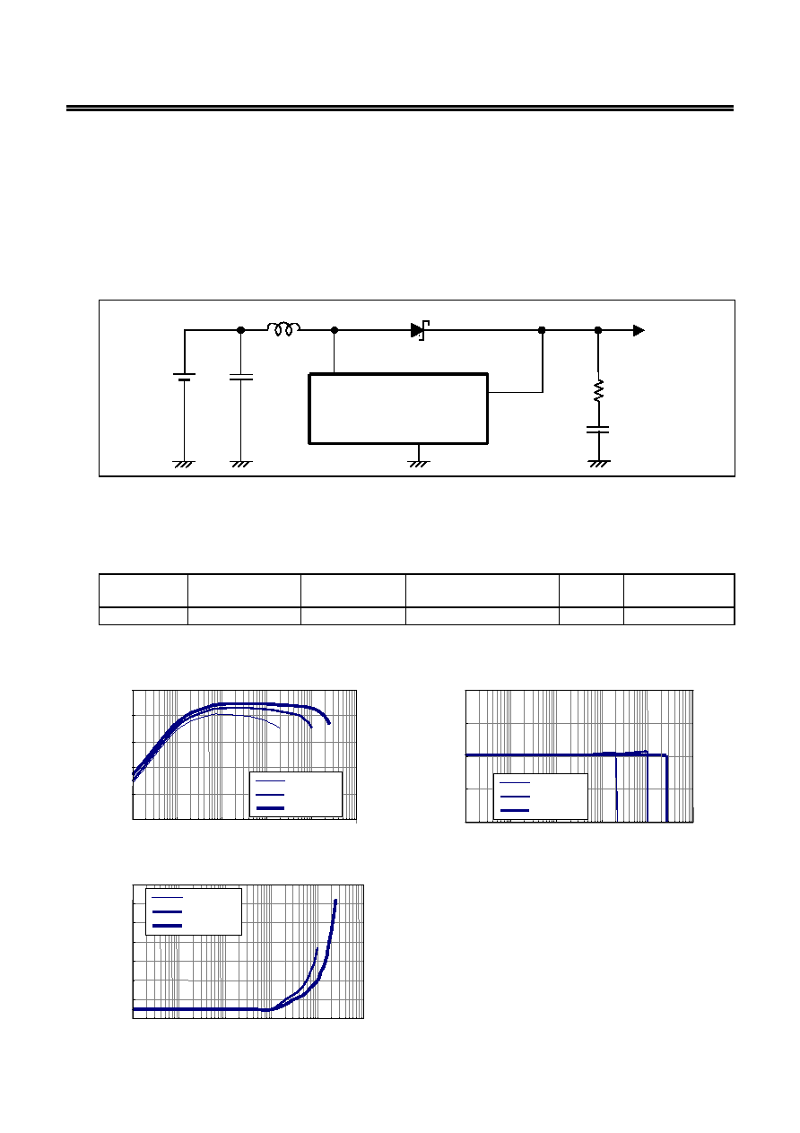
Example of Ceramic Capacitor Application
When using a component with a small ESR, such as a ceramic capacitor, for the output capacitance,
mount a resistor (R
1
) equivalent to the ESR in series with the ceramic capacitor (C
L
) as shown in Figure
16.
R1 differs depending on the L value, capacitance, wiring, and application (output load).
The following example shows a circuit using R
1
=100 m, output voltage=3.3 V, output load=100 mA and its
characteristics.
CONT
VOUT
VSS
V
OUT
SD
C
L
L
R
1
V
IN
C
IN
Caution The above connection diagram and constant will not guarantees successful operation.
Perform through evaluation using the actual application to set the constant.
Figure 16 Circuit Using Ceramic Capacitor
Table 15
IC
L type name
SD type name
C
L
(Ceramic capacitor)
R
1
Output
Characteristics
S-8353A33 CDRH5D28-101 MA2Z748
10
µF◊2 100
m
(a), (b), (c)
Ceramic Capacitor Circuit Output Characteristics
1. Output current-Efficiency
2. Output current-Output voltage
V
IN
=1.8
V
IN
=2.7
V
IN
=0.9
0
20
40
60
80
100
0.01 0.1 1 10 100 1000
Output current I
OUT
[mA]
E
ffic
i
enc
y
[%
]
3.20
3.25
3.30
3.35
3.40
0.01 0.1 1 10 100 1000
Output current I
OUT
[mA]
Ou
tp
u
t
v
o
l
t
a
g
e
V
OU
T
[
V
]
V
IN
=1.8
V
IN
=2.7
V
IN
=0.9
3. Output current-Ripple voltage
0
20
40
60
80
100
120
0.01 0.1 1 10 100 1000
R
i
pp
le v
o
lt
a
ge
V
r
[m
V
]
Output current I
OUT
[mA]
140
V
IN
=1.8
V
IN
=2.7
V
IN
=0.9
ULTRA-SMALL PACKAGE PWM CONTROL, PWM/PFM SWITCHING CONTROL STEP-UP SWITCHING REGULATOR
Rev.1.2
_00
S-8353/8354 Series
Seiko Instruments Inc.
23
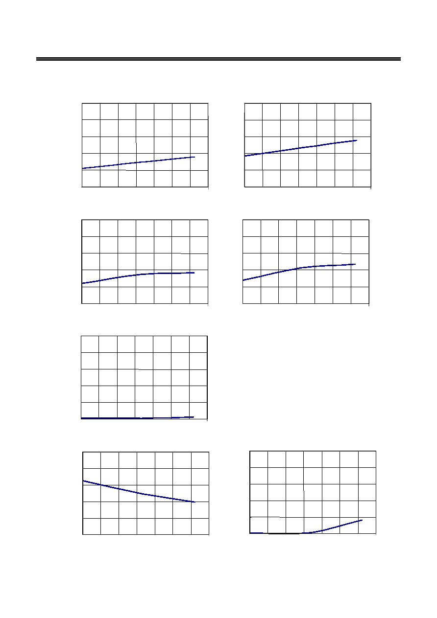
Examples of Major Temperature Characteristics (Ta
=-
=-
=-
=-40 to ++++85∞∞∞∞C)
I
SS1
- T
a
(V
OUT
= 3.3 V, f
osc
= 50 kHz)
0
10
20
30
40
50
-40 -20 0 20 40 60 80 100
T
a
[∞C]
I
SS1
[
µA]
I
SS1
- T
a
(V
OUT
= 3.3 V, f
osc
= 250 kHz)
0
20
40
60
80
100
-40 -20 0 20 40 60 80 100
T
a
[∞C]
I
SS1
[
µA]
I
SS2
- T
a
(V
OUT
= 3.3 V, f
osc
= 50 kHz)
0
2
4
6
8
10
-40 -20 0 20 40 60 80 100
T
a
[∞C]
I
SS2
[
µA]
I
SS2
- T
a
(V
OUT
= 3.3 V, f
osc
= 250 kHz)
0
2
4
6
8
10
-40 -20 0 20 40 60 80 100
T
a
[∞C]
I
SS2
[
µA]
I
SSS
- T
a
(V
OUT
= 3.3 V, f
osc
= 250 kHz)
0.0
0.2
0.4
0.6
0.8
1.0
-40 -20 0 20 40 60 80 100
T
a
[∞C]
I
SSS
[
µA]
I
SW
-T
a
(V
OUT
= 3.3 V,f
osc
= 250 kHz)
-40 -20 0 20 40 60 80 100
T
a
[∞C]
I
SW
[mA]
100
200
300
400
500
0
I
SWQ
-T
a
(V
OUT
= 3.3 V,f
osc
= 250 kHz)
0.0
0.2
0.4
0.6
0.8
1.0
-40 -20 0 20 40 60 80 100
T
a
[∞C]
I
SWQ
[
µA]
ULTRA-SMALL PACKAGE PWM CONTROL, PWM/PFM SWITCHING CONTROL STEP-UP SWITCHING REGULATOR
S-8353/8354 Series
Rev.1.2
_00
24
Seiko Instruments Inc.
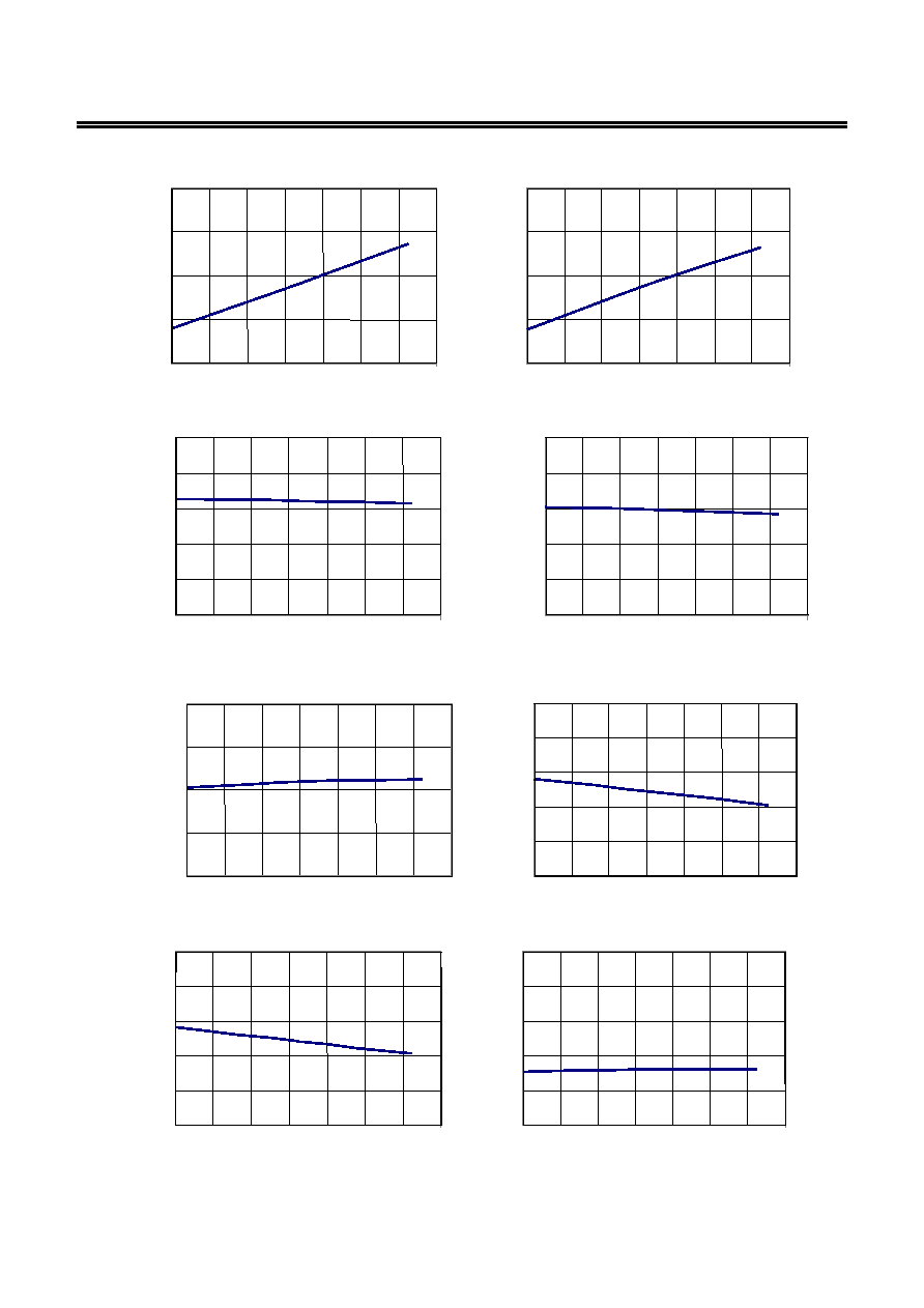
f
osc
- T
a
(V
OUT
= 3.3 V, f
osc
= 50 kHz)
30
40
50
60
70
-40 -20 0 20 40 60 80 100
T
a
[∞C]
f
osc
[kHz]
f
osc
- T
a
(V
OUT
= 3.3 V, f
osc
= 250 kHz)
150
200
250
300
350
-40 -20 0 20 40 60 80 100
T
a
[∞C]
f
osc
[kHz]
MaxDuty
- T
a
(V
OUT
= 3.3 V, f
osc
= 50 kHz)
-40 -20 0 20 40 60 80 100
T
a
[∞C]
MaxDuty
[%]
50
60
70
80
90
100
MaxDuty
- T
a
(V
OUT
= 3.3 V, f
osc
= 250 kHz)
-40 -20 0 20 40 60 80 100
T
a
[∞C]
MaxDuty
[%]
50
60
70
80
90
100
PFMDuty
- T
a
(V
OUT
= 3.3 V, f
osc
= 250 kHz)
5
10
15
20
25
-40 -20 0 20 40 60 80 100
T
a
[∞C]
PFMDuty
[%]
S-8354 Series
V
SH
- T
a
(V
OUT
= 3.3 V, f
osc
= 250 kHz)
0.0
0.2
0.4
0.6
0.8
1.0
-40 -20 0 20 40 60 80 100
T
a
[∞C]
V
SH
[V]
V
SL1
- T
a
(V
OUT
= 3.3 V, f
osc
= 250 kHz)
0.0
0.2
0.4
0.6
0.8
1.0
-40 -20 0 20 40 60 80 100
T
a
[∞C]
V
SL1
[V]
V
SL2
- T
a
(V
OUT
= 3.3 V, f
osc
= 250 kHz)
0.0
0.2
0.4
0.6
0.8
1.0
-40 -20 0 20 40 60 80 100
T
a
[∞C]
V
SL2
[V]

ULTRA-SMALL PACKAGE PWM CONTROL, PWM/PFM SWITCHING CONTROL STEP-UP SWITCHING REGULATOR
Rev.1.2
_00
S-8353/8354 Series
Seiko Instruments Inc.
25
T
SS
vs. Ta (V
OUT
= 3.3 V, f
OSC
= 50 kHz)
0
2
4
6
8
-40 -20
0
20
40
60
80
100
Ta [
∞C]
T
SS
[ms]
V
ST1
vs. Ta (V
OUT
= 3.3 V, f
OSC
= 250 kHz)
0.0
0.2
0.4
0.6
0.8
1.0
1.2
-40 -20
0
20
40
60
80
100
Ta [
∞C]
V
ST1
[V]
T
SS
vs. Ta (V
OUT
= 3.3 V, f
OSC
= 250 kHz)
0
2
4
6
8
-40 -20
0
20
40
60
80
100
Ta [
∞C]
T
SS
[ms]
V
ST2
vs. Ta (V
OUT
= 3.3 V, f
OSC
= 250 kHz)
0.0
0.2
0.4
0.6
0.8
1.0
1.2
-40 -20
0
20
40
60
80
100
Ta [
∞C]
V
ST2
[V]
V
OUT
vs. Ta (V
OUT
= 3.3 V, f
OSC
= 50 kHz)
3.20
3.25
3.30
3.35
3.40
-40 -20
0
20
40
60
80
100
Ta [
∞C]
V
OUT
[V]
V
OUT
vs. Ta (V
OUT
= 3.3 V, f
OSC
= 250 kHz)
3.20
3.25
3.30
3.35
3.40
-40 -20
0
20
40
60
80
100
Ta [
∞C]
V
OUT
[V]
ULTRA-SMALL PACKAGE PWM CONTROL, PWM/PFM SWITCHING CONTROL STEP-UP SWITCHING REGULATOR
S-8353/8354 Series
Rev.1.2
_00
26
Seiko Instruments Inc.
Examples of Major Power Supply Dependence Characteristics (Ta
=
=
=
=25∞∞∞∞C)
I
SS1,2
- V
DD
(V
OUT
= 3.3 V, f
OSC
= 50 kHz, T
a
= 25∞C)
0
10
20
30
40
50
0 2 4 6 8 10
V
DD
[V]
I
SS1,2
[
µA]
I
SSS
- V
DD
(V
OUT
= 3.3 V, f
OSC
= 250 kHz, T
a
= 25∞C)
0
20
40
60
80
100
0 2 4 6 8 10
V
DD
[V]
I
SSS
[
µA]
f
OSC
- V
DD
(f
OSC
= 50 kHz)
30
40
50
60
70
0 2 4 6 8 10
V
DD
[V]
f
osc
[kHz]
f
OSC
- V
DD
(f
OSC
= 250 kHz)
100
150
200
250
300
0 2 4 6 8 10
V
DD
[V]
f
osc
[kHz]
I
SW
- V
DD
-
0 2 4 6 8 10
V
DD
[V]
I
SW
[mA]
100
200
300
400
500
0
V
DD
[V]
V
OUT
[V]
3.0
3.1
3.2
3.3
3.4
0 2 4 6 8 10
V
OUT
- V
DD
(V
OUT
= 3.3 V, f
OSC
= 50 kHz, V
DD
separate type)
V
IN
= 1.98 V, I
OUT
= 13.2 mA
0 2 4 6 8 10
V
DD
[V]
V
OUT
[V]
V
OUT
- V
DD
(V
OUT
= 3.3 V, f
OSC
= 250 kHz, V
DD
separate type)
V
IN
= 1.98 V, I
OUT
= 13.2 mA
3.0
3.1
3.2
3.3
3.4
ULTRA-SMALL PACKAGE PWM CONTROL, PWM/PFM SWITCHING CONTROL STEP-UP SWITCHING REGULATOR
Rev.1.2
_00
S-8353/8354 Series
Seiko Instruments Inc.
27
Output Waveforms
1. S-8353A33
t [10
µs/div]
Output voltage
[0.01 V/div]
CONT voltage
[1 V/div]
t [10
µs/div]
Output voltage
[0.01 V/div]
CONT voltage
[1 V/div]
2. I
OUT
=50 mA, V
IN
=1.98 V
1. I
OUT
=10 mA, V
IN
=1.98 V
t [10
µs/div]
Output voltage
[0.02 V/div]
CONT voltage
[1 V/div]
3. I
OUT
=100 mA, V
IN
=1.98 V
2. S-8354H33
t [2
µ
s/div]
4
2
0
Output voltage
[0.01 V/div]
CONT
voltage
[1 V/div]
1. I
OUT
= 100 µ A V
IN
= 1.98 V
t [2
µ
s/div]
Output voltage
[0.01 V/div]
CONT voltage
[1 V/div]
t [2
µ
s/div]
Output voltage
[0.02 V/div]
CONT
voltage
[1 V/div]
Output voltage
[0.02 V/div]
CONT
voltage
[1 V/div]
t [2
µ
s/div]
4
2
0
4
2
0
4
2
0
2 . I
OUT
= 10 mA V
IN
= 1.98 V
3 . I
OUT
= 50 mA V
IN
= 1.98 V
4 . I
OUT
= 100 mA V
IN
= 1.98 V
ULTRA-SMALL PACKAGE PWM CONTROL, PWM/PFM SWITCHING CONTROL STEP-UP SWITCHING REGULATOR
S-8353/8354 Series
Rev.1.2
_00
28
Seiko Instruments Inc.
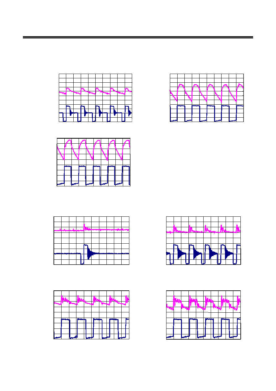
Examples of Transient Response Characteristics (Ta
=
=
=
=25∞∞∞∞C) (S-8354H33)
1. Power-On (V
IN
; 0 V
2.0 V)
0
2
t (1 ms/div)
V
IN
[V]
0
2
4
V
OUT
[V]
0
2
V
IN
[V]
0
2
4
V
OUT
[V]
t (1 ms/div)
2.
OFF
ON/
Pin Response (V
ON/OFF
; 0 V
2.0 V)
ON/OFF (250 kHz, I
OUT
= 1 mA, V
IN
= 2 V)
0
2
t (1 ms/div)
0
2
4
V
OUT
[V]
0
2
0
2
4
V
OUT
[V]
t (1 ms/div)
[V]
V
ON/OFF
[V]
V
ON/OFF
ON/OFF (250 kHz, I
OUT
= 50 mA, V
IN
= 2 V)
3. Load Fluctuations
V
OUT
V
OUT
[0.05 V/div]
100
µA
50 mA
[0.05 V/div]
I
OUT
I
OUT
(250 kHz, I
OUT
; 100
µA 50 mA, V
IN
= 1.98 V)
(250 kHz, I
OUT
; 50 mA
100 µA, V
IN
= 1.98 V)
Load Fiuctuation
Load Fiuctuation
t (200
µs/div)
t (5 ms/div)
100
µA
50 mA
4. Input Voltage Fluctuations
1.98
2.64
V
IN
[V]
1.98
2.64
V
IN
[V]
Input voltage fluctuation (250 kHz, I
OUT
= 50 mA)
V
IN
= 1.98 V 2.64 V
Input voltage fluctuation (250 kHz, I
OUT
= 50 mA)
V
IN
= 2.64 V 1.98 V
t (100
µs/div)
t (100
µs/div)
V
OUT
[0.04 V/div]
V
OUT
[0.02 V/div]
ULTRA-SMALL PACKAGE PWM CONTROL, PWM/PFM SWITCHING CONTROL STEP-UP SWITCHING REGULATOR
Rev.1.2
_00
S-8353/8354 Series
Seiko Instruments Inc.
29
Reference Data
Reference data is provided to determine specific external components. Therefore, the following data shows
the characteristics of the recommended external components selected for various applications.
1. Reference Data for External Components
Table 16 Efficiency vs. Output Characteristics and Output Voltage vs. Output Current Characteristics
for External Components
No. Product
name
Oscillation
frequency
[kHz]
Output voltage
[V]
Control system
Inductor
Diode
Output capacitor
1 S-8353H50MC 250
5.0
PWM
CDRH8D28-220 MA2Z748 F93 (16 V, 47
µF)
2 S-8353H50MC 250
5.0
PWM
CDRH5D28-220 MA2Z748 F93 (6.3 V, 22
µF)
3 S-8353H50MC 250
5.0
PWM
CXLP120-220 MA2Z748 F92 (6.3 V, 47
µF)
4 S-8354A50MC
50
5.0
PWM/PFM CDRH8D28-101 MA2Z748 F93 (6.3 V, 22
µF)
5 S-8354A50MC
50
5.0
PWM/PFM
CXLP120-470 MA2Z748 F92 (6.3 V, 47
µF)
6 S-8353A50MC
50
5.0
PWM
CDRH8D28-101 MA2Z748 F93 (6.3 V, 22
µF)
7 S-8353A50MC
50
5.0
PWM
CXLP120-470 MA2Z748 F92 (6.3 V, 47
µF)
8 S-8353A33MC
50
3.3
PWM
CDRH8D28-101 MA2Z748 F93 (6.3 V, 22
µF)
The performance of the external components is shown below.
Table 17 Properties of External Components
Component Product
name
Manufacturer
Characteristics
Inductor CDRH8D28-220 Sumida
Corporation
22
µH, DCR
*1
=95 m, Imax.
*2
=1.6 A,
Component height
=3.0 mm
CDRH8D28-101
100
µH, DCR
*1
=410 m, Imax.
*2
=0.75 A,
Component height
=3.0 mm
CDRH5D28-220
22
µH, DCR
*1
=122 m, Imax.
*2
=0.9 A,
Component height
=3.0 mm
CXLP120-220
Sumitomo Special Metals
Co., Ltd.
22
µH, DCR
*1
=590 m
, Imax.
*2
=0.55 A,
Component height
=1.2 mm
CXLP120-470
47
µH, DCR
*1
=950 m, Imax.
*2
=0.45 A,
Component height
=1.2 mm
Diode MA2Z748
Matsushita Electric
Industrial Co., Ltd,
V
F
*3
=0.4 V, I
F
*4
=0.3 A
Capacitor
F93 (16 V, 47
µF)
Nichicon Corporation
F93 (6.3 V, 22
µF)
F92 (6.3 V, 47
µF)
*1. DC resistance
*2. Maximum allowable current
*3. Forward voltage
*4. Forward current
Caution The values shown in the characteristics column of Table 17 above are based on the
materials provided by each manufacturer, however, consider the characteristics of the
original materials when using the above products.
ULTRA-SMALL PACKAGE PWM CONTROL, PWM/PFM SWITCHING CONTROL STEP-UP SWITCHING REGULATOR
S-8353/8354 Series
Rev.1.2
_00
30
Seiko Instruments Inc.
2. Reference Data (1)
The following shows the actual (a) Output current vs. Efficiency characteristics and (b) Output current vs.
Output voltage characteristics under the conditions of No. 1 to 8 in Table 16.
(1) S-8353H50MC
4.7
4.8
4.9
5.0
5.1
5.2
20
40
60
80
100
Output current I
OUT
[mA]
(b) Output current vs. Output voltage
E
ffici
en
cy
[%]
(a) Output current vs. Efficiency
Output current I
OUT
[mA]
O
u
tput
v
o
ltage V
OUT
[V]
V
IN
= 2 V
V
IN
= 3 V
V
IN
= 4 V
1
10
100
1000
0.1
0.01
1
10
100
1000
0.1
0.01
V
IN
= 2 V
V
IN
= 3 V
V
IN
= 4 V
(2) S-8353H50MC
4.7
4.8
4.9
5.0
5.1
5.2
20
40
60
80
100
Output current I
OUT
[mA]
(b) Output current vs. Output voltage
E
ffici
en
cy
[%]
(a) Output current vs. Efficiency
Output current I
OUT
[mA]
O
u
tput
v
o
ltage
V
OUT
[V]
1
10
100
1000
0.1
0.01
1
10
100
1000
0.1
0.01
V
IN
= 2 V
V
IN
= 3 V
V
IN
= 4 V
V
IN
= 2 V
V
IN
= 3 V
V
IN
= 4 V
(3) S-8353H50MC
20
40
60
80
100
4.7
4.8
4.9
5.0
5.1
5.2
Output current I
OUT
[mA]
(b) Output current vs. Output voltage
E
ffici
en
cy
[%]
(a) Output current vs. Efficiency
Output current I
OUT
[mA]
O
u
tput
v
o
ltage
V
OUT
[V]
1
10
100
1000
0.1
0.01
1
10
100
1000
0.1
0.01
V
IN
= 2 V
V
IN
= 3 V
V
IN
= 4 V
V
IN
= 2 V
V
IN
= 3 V
V
IN
= 4 V

ULTRA-SMALL PACKAGE PWM CONTROL, PWM/PFM SWITCHING CONTROL STEP-UP SWITCHING REGULATOR
Rev.1.2
_00
S-8353/8354 Series
Seiko Instruments Inc.
31
(4) S-8354A50MC
20
40
60
80
100
Output current I
OUT
[mA]
(b) Output current vs. Output voltage
E
ffici
en
cy
[%]
(a) Output current vs. Efficiency
Output current I
OUT
[mA]
O
u
tput
v
o
ltage
V
OUT
[V]
4.7
4.8
4.9
5.0
5.1
5.2
1
10
100
1000
0.1
0.01
1
10
100
1000
0.1
0.01
V
IN
= 2 V
V
IN
= 3 V
V
IN
= 4 V
V
IN
= 2 V
V
IN
= 3 V
V
IN
= 4 V
(5) S-8354A50MC
20
40
60
80
100
Output current I
OUT
[mA]
(b) Output current vs. Output voltage
E
ffici
en
cy
[%]
(a) Output current vs. Efficiency
Output current I
OUT
[mA]
O
u
tput
v
o
ltage
V
OUT
[V]
4.7
4.8
4.9
5.0
5.1
5.2
1
10
100
1000
0.1
0.01
1
10
100
1000
0.1
0.01
V
IN
= 2 V
V
IN
= 3 V
V
IN
= 4 V
V
IN
= 2 V
V
IN
= 3 V
V
IN
= 4 V
(6) S-8353A50MC
Output current I
OUT
[mA]
(b) Output current vs. Output voltage
E
ffici
en
cy
[%]
(a) Output current vs. Efficiency
Output current I
OUT
[mA]
O
u
tput
v
o
ltage
V
OUT
[V]
20
40
60
80
100
4.7
4.8
4.9
5.0
5.1
5.2
1
10
100
1000
0.1
0.01
1
10
100
1000
0.1
0.01
V
IN
= 2 V
V
IN
= 3 V
V
IN
= 4 V
V
IN
= 2 V
V
IN
= 3 V
V
IN
= 4 V

ULTRA-SMALL PACKAGE PWM CONTROL, PWM/PFM SWITCHING CONTROL STEP-UP SWITCHING REGULATOR
S-8353/8354 Series
Rev.1.2
_00
32
Seiko Instruments Inc.
(7) S-8353A50MC
Output
current
I
OUT
[
mA]
( b) Output current vs. O utput voltage
E
ffici
en
cy
[%]
( a) Output current vs. E fficiency
Output
current
I
OUT
[
mA]
O
u
tput v
o
lt
age
V
OUT
[V]
20
40
60
80
100
4.7
4.8
4.9
5.0
5.1
5.2
1
10
100
1000
0.1
0.01
V
IN
=
2 V
V
IN
=
3 V
V
IN
=
4 V
V
IN
=
2 V
V
IN
=
3 V
V
IN
=
4 V
1
10
100
1000
0.1
0.01
(8) S-8354A33MC
Output
current
I
OUT
[
mA]
( b) Output current vs. O utput voltage
E
ffici
en
cy
[%]
( a) Output current vs. E fficiency
Output
current
I
OUT
[
mA]
O
u
tput
v
o
ltage
V
OUT
[V]
20
40
60
80
100
3.0
3.1
3.2
3.3
3.4
3.5
1
10
100
1000
0.1
0.01
V
IN
= 0.9 V
V
IN
= 1.8 V
V
IN
= 2.7 V
V
IN
= 0.9 V
V
IN
= 1.8 V
V
IN
= 2.7 V
1
10
100
1000
0.1
0.01
ULTRA-SMALL PACKAGE PWM CONTROL, PWM/PFM SWITCHING CONTROL STEP-UP SWITCHING REGULATOR
Rev.1.2
_00
S-8353/8354 Series
Seiko Instruments Inc.
33
3. Reference Data (2)
The following shows the actual output current vs. ripple voltage characteristics under the conditions of No.
1 to 8 in Table 16.
(1) S-8353H50MC
(2) S-8353H50MC
Output current I
OUT
[mA]
Output current vs. Ripple voltage
R
i
pple
v
o
ltage
Vr [mV]
Output current vs. Ripple voltage
Output current I
OUT
[mA]
R
i
pple
v
o
ltage
Vr [mV]
1
10
100
1000
0.1
0.01
V
IN
= 2 V
V
IN
= 3 V
V
IN
= 4 V
V
IN
= 2 V
V
IN
= 3 V
V
IN
= 4 V
20
40
60
80
100
0
1
10
100
1000
0.1
0.01
20
40
60
80
100
0
(3) S-8353H50MC
(4) S-8354A50MC
Output current I
OUT
[mA]
Output current vs. Ripple voltage
R
i
pple
v
oltage
Vr [mV]
Output current vs. Ripple voltage
Output current I
OUT
[mA]
R
i
pple
v
oltage
Vr [mV]
1
10
100
1000
0.1
0.01
V
IN
= 2 V
V
IN
= 3 V
V
IN
= 4 V
V
IN
= 2 V
V
IN
= 3 V
V
IN
= 4 V
40
80
120
160
200
0
1
10
100
1000
0.1
0.01
40
80
120
160
200
0
(5) S-8354A50MC
(6) S-8353A50MC
Output current I
OUT
[mA]
Output current vs. Ripple voltage
R
i
pple
v
oltage
Vr [mV]
Output current vs. Ripple voltage
Output current I
OUT
[mA]
R
i
pple
v
oltage
Vr [mV]
1
10
100
1000
0.1
0.01
V
IN
= 2 V
V
IN
= 3 V
V
IN
= 4 V
V
IN
= 2 V
V
IN
= 3 V
V
IN
= 4 V
1
10
100
1000
0.1
0.01
40
80
120
160
200
0
40
80
120
160
200
0
240
280
ULTRA-SMALL PACKAGE PWM CONTROL, PWM/PFM SWITCHING CONTROL STEP-UP SWITCHING REGULATOR
S-8353/8354 Series
Rev.1.2
_00
34
Seiko Instruments Inc.
(7) S-8353A50MC
(8) S-8353A33MC
Output current I
OUT
[mA]
Output current vs. ripple voltage
R
i
pple
v
oltage
Vr [mV]
Output current vs. ripple voltage
Output current I
OUT
[mA]
R
i
pple
v
oltage
Vr [mV]
1
10
100
1000
0.1
0.01
V
IN
= 2 V
V
IN
= 3 V
V
IN
= 4 V
1
10
100
1000
0.1
0.01
40
80
120
160
200
0
40
80
120
160
200
0
240
280
V
IN
= 0.9 V
V
IN
= 1.8 V
V
IN
= 2.7 V
No.
TITLE
SCALE
UNIT
mm
Seiko Instruments Inc.
2.9±0.2
0.95±0.1
1.9±0.2
+0.1
-0.05
0.16
0.4±0.1
1
2
3
No. MP003-A-P-SD-1.1
MP003-A-P-SD-1.1
SOT233-A-PKG Dimensions
No.
TITLE
SCALE
UNIT
mm
Seiko Instruments Inc.
1.6±0.1
0.25±0.05
4.0±0.1
2.0±0.1
4.0±0.1
1.5
+0.1
-0.05
1.1±0.1
2.85±0.2
No. MP003-A-C-SD-1.1
MP003-A-C-SD-1.1
SOT233-A-Carrier Tape
Feed direction
1
2
3

No.
TITLE
SCALE
UNIT
mm
Seiko Instruments Inc.
(60∞)
(60∞)
¯13±0.2
12.5max.
9.0±0.3
QTY.
3,000
No. MP003-A-R-SD-1.1
MP003-A-R-SD-1.1
SOT233-A-Reel
Enlarged drawing in the central part

No.
TITLE
SCALE
UNIT
mm
Seiko Instruments Inc.
2.9±0.2
1.9±0.2
0.95±0.1
0.4±0.1
0.16
+0.1
-0.06
1
2
3
4
5
No. MP005-A-P-SD-1.2
MP005-A-P-SD-1.2
SOT235-A-PKG Dimensions
No.
TITLE
SCALE
UNIT
mm
Seiko Instruments Inc.
¯1.5
+0.1
-0
2.0±0.05
¯1.0
+0.2
-0
4.0±0.1
1.4±0.2
0.25±0.1
3.2±0.2
1
2
3
4
5
No. MP005-A-C-SD-2.1
MP005-A-C-SD-2.1
SOT235-A-Carrier Tape
Feed direction
4.0±0.1(10 pitches:40.0±0.2)

No.
TITLE
SCALE
UNIT
mm
Seiko Instruments Inc.
12.5max.
9.0±0.3
¯13±0.2
(60∞)
(60∞)
QTY.
3,000
No. MP005-A-R-SD-1.1
MP005-A-R-SD-1.1
SOT235-A-Reel
Enlarged drawing in the central part
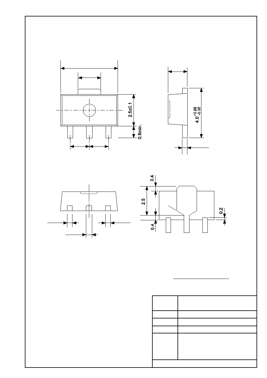
No.
TITLE
SCALE
UNIT
mm
Seiko Instruments Inc.
0.4±0.05
1.5±0.1
4.5±0.1
1.6±0.2
1.5±0.1 1.5±0.1
0.45±0.1
0.4±0.1
0.4±0.1
45∞
3
1
2
No. UP003-A-P-SD-1.1
UP003-A-P-SD-1.1
SOT893-A-PKG Dimensions
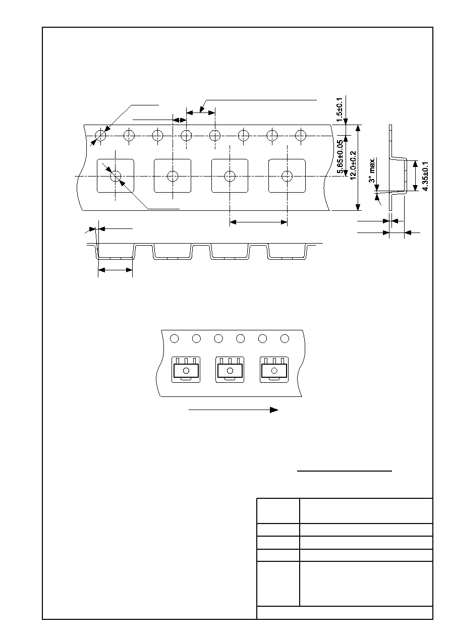
No.
TITLE
SCALE
UNIT
mm
Seiko Instruments Inc.
2.0±0.1
0.3±0.05
8.0±0.1
¯1.5
+0.1
-0
2.0±0.05
¯1.5
+0.1
-0
4.75±0.1
5∞ max.
No. UP003-A-C-SD-1.1
UP003-A-C-SD-1.1
SOT893-A-Carrier Tape
Feed direction
4.0±0.1(10 pitches : 40.0±0.2)
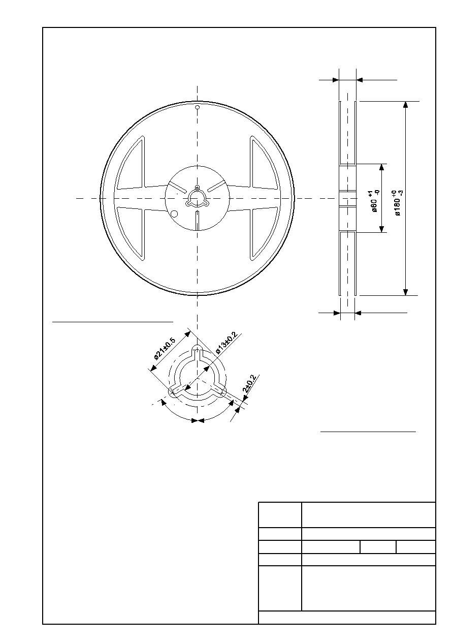
No.
TITLE
SCALE
UNIT
mm
Seiko Instruments Inc.
13.0±0.3
16.5max.
(60∞)
(60∞)
QTY.
1,000
No. UP003-A-R-SD-1.1
UP003-A-R-SD-1.1
SOT893-A-Reel
Enlarged drawing in the central part

∑
The information described herein is subject to change without notice.
∑
Seiko Instruments Inc. is not responsible for any problems caused by circuits or diagrams described herein
whose related industrial properties, patents, or other rights belong to third parties. The application circuit
examples explain typical applications of the products, and do not guarantee the success of any specific
mass-production design.
∑
When the products described herein are regulated products subject to the Wassenaar Arrangement or other
agreements, they may not be exported without authorization from the appropriate governmental authority.
∑
Use of the information described herein for other purposes and/or reproduction or copying without the
express permission of Seiko Instruments Inc. is strictly prohibited.
∑
The products described herein cannot be used as part of any device or equipment affecting the human
body, such as exercise equipment, medical equipment, security systems, gas equipment, or any apparatus
installed in airplanes and other vehicles, without prior written permission of Seiko Instruments Inc.
∑
Although Seiko Instruments Inc. exerts the greatest possible effort to ensure high quality and reliability, the
failure or malfunction of semiconductor products may occur. The user of these products should therefore
give thorough consideration to safety design, including redundancy, fire-prevention measures, and
malfunction prevention, to prevent any accidents, fires, or community damage that may ensue.