S8425_E1.1_10

Rev.1.1
_10
BATTERY BACKUP SWITCHING IC
S-8425 Series
Seiko Instruments Inc.
1
The S-8425 Series is a CMOS IC designed for use in the
switching circuits of primary and backup power supplies on
a single chip. It consists of three voltage regulators, two
voltage detectors, a power supply switch and its controller,
as well as other functions.
In addition to the function for switching between the primary
and backup power supply, the S-8425 Series can provide
microcontrollers with two types of voltage detection output
signals corresponding to the power supply voltage.
Moreover, adopting a special sequence for switch control
enables the effective use of the backup power supply,
making this IC ideal for configuring a backup system.
Features
· Low power consumption
Normal
operation: 15
µA max. (V
IN
= 6 V)
Backup:
2.1
µA max.
· Voltage regulator
Output voltage tolerance :
±2%
Output voltage:
Independently selectable in 0.1 V steps in the range of 2.3 V to 5.4 V
· Two built-in voltage detectors (CS, RESET)
Detection voltage tolerance:
±2%
Detection voltage: Selectable in 0.1 V steps in the range of 2.4 V to 5.3 V (CS voltage
detector)
Selectable in 0.1 V steps in the range of 1.7 V to 3.4 V (RESET voltage
detector)
· RESET release delay: 300 µs min.
· Switching circuit for primary power supply and backup power supply configurable on one chip
· Efficient use of backup power supply possible
· Special sequence
Backup voltage is not output when the primary power supply voltage does not reach the initial
voltage at which the switch unit operates.
Package
· 8-Pin TSSOP (Package drawing No.: FT008-A)
· 8-Pin SON(B) (Package drawing No.: PA008-B)
Applications
· Camcorders
· Digital cameras
· Memory cards
· SRAM backup equipment

BATTERY BACKUP SWITCHING IC
S-8425 Series
Rev.1.1
_10
Seiko Instruments Inc.
2
Selection Guide
Part No. Package
Output Voltage (V)
CS Voltage (V) RESET Voltage
(V)
Switch Voltage
(V)
Type
V
RO
V
OUT
V
CH
-V
DET1
+V
DET1
-V
DET2
+V
DET2
V
SW1
S-8425AAAFT-TB 8-Pin
TSSOP
3.000 3.000 3.300 3.300 3.401 2.200 2.312 +V
DET1
× 0.85
S-8425AAAPA-TF 8-Pin
SON(B)
3.000 3.000 3.300 3.300 3.401 2.200 2.312 +V
DET1
× 0.85
Caution Set the CS voltage so that the switch voltage (V
SW1
) is equal to or greater than the
RESET detection voltage (
-
-
-
-V
DET2
).
Remark The selection range is as follows.
V
RO
, V
OUT
, V
CH
: 2.3 to 5.4 V (0.1 V steps)
-V
DET1
:
2.4 to 5.3 V (0.1 V steps)
-V
DET2
:
1.7 to 3.4 V (0.1 V steps )
V
SW1
:
+V
DET1
× 0.85 or +V
DET1
× 0.77
If a product with a voltage other than above is required, contact our sales representative.
S-8425 A xx xx - xx
IC orientation for taping specifications
TB: 8-Pin TSSOP
TF: 8-Pin SON(B)
Package
code
FT: 8-Pin TSSOP
PA: 8-Pin SON(B)
Serial code
BATTERY BACKUP SWITCHING IC
Rev.1.1
_10
S-8425 Series
Seiko Instruments Inc.
3
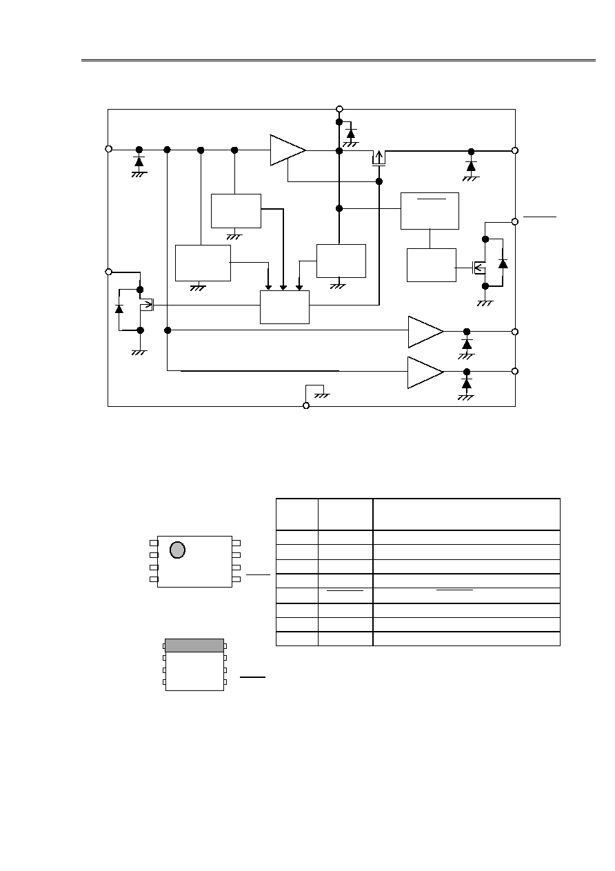
Block Diagram
VBAT
V
SW2
detector
M1
CS
Voltage
detector
V
SW1
detector
Switch
controller
VOUT
RESET
RESET
Voltage
detector
Delay
circuit
CS
VIN
REG2
REG1
VRO
VSS
REG3
VCH
Figure 1 Block Diagram
Pin Assignment
VSS
VCH
VBAT
CS
VRO
VIN
VOUT
RESET
8-Pin TSSOP
Top View
1
2
3
4
8
7
6
5
VSS
VCH
VBAT
CS
VRO
VIN
VOUT
RESET
8-Pin SON(B)
Top View
8
7
6
5
1
2
3
4
*1
Mount capacitors between VSS (GND) and the VIN, VBAT, VOUT, VRO, and VCH pins
(see the Standard Circuit section).
Pin
No.
Pin Name
Functions
1 VSS
Ground
2 VCH
*1
Output pin of voltage regulator 3
3 VBAT
*1
Backup power supply input pin
4
CS
Output pin of CS voltage detector
5
RESET
Output pin of RESET voltage detector
6 VOUT
*1
Output pin of voltage regulator 2
7 VIN
*1
Primary power supply input pin
8 VRO
*1
Output pin of voltage regulator 1
Figure 2 Pin Placement
BATTERY BACKUP SWITCHING IC
S-8425 Series
Rev.1.1
_10
Seiko Instruments Inc.
4
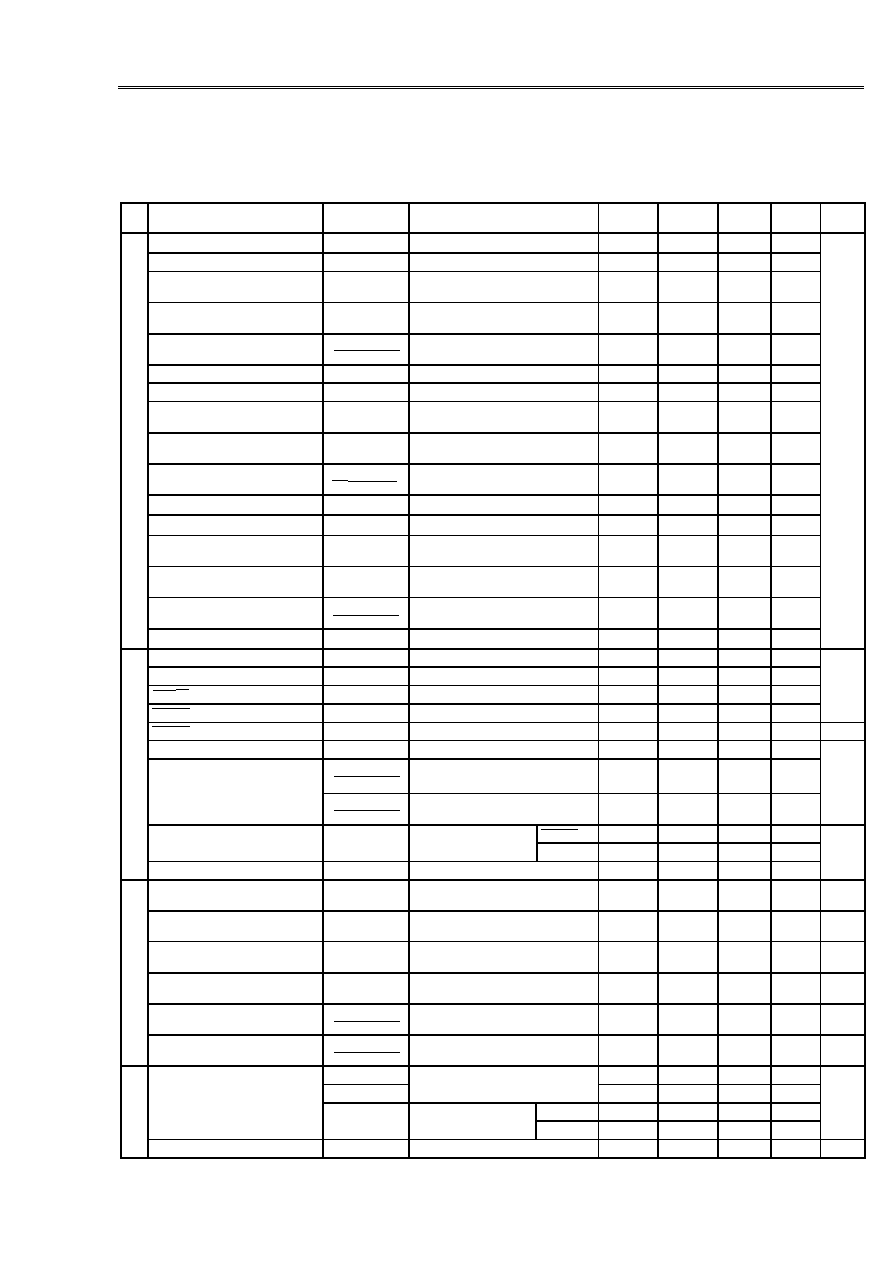
Absolute Maximum Ratings
Table 1 Absolute Maximum Ratings
(Ta
= 25°C, unless otherwise specified)
Parameter Symbol
Ratings
Unit
Primary power supply input voltage
V
IN
V
SS
-0.3 to V
SS
+18 V
Backup power supply input voltage
V
BAT
V
SS
-0.3 to V
SS
+18 V
Output voltage of voltage regulator
V
RO
, V
OUT
, V
CH
V
SS
-0.3 to V
IN
+0.3 V
CS output voltage
V
CS
RESET output voltage
V
RESET
8-Pin TSSOP
300
mW
Power dissipation
P
D
8-Pin SON(B)
300
Operating ambient temperature
T
opr
-40 to +85
°C
Storage temperature
T
stg
-40 to +125
°C
Caution The absolute maximum ratings are rated values exceeding which the product
could suffer physical damage. These values must therefore not be exceeded
under any conditions.
V
SS
-0.3 to V
SS
+18
V
BATTERY BACKUP SWITCHING IC
Rev.1.1
_10
S-8425 Series
Seiko Instruments Inc.
5
Electrical Characteristics
S-8425AAAFT, S-8425AAAPA
Table 2 Electrical Characteristics
(Ta
= 25°C, Unless otherwise specified)
Parameter
Symbol
Conditions
Min.
Typ.
Max.
Unit
Test
Circuit
Output voltage 1
V
RO
V
IN
= 7.2 V, I
RO
= 3 mA
2.940 3.000 3.060 V
Dropout voltage 1
V
drop1
I
RO
= 3 mA
-
41 59
mV
Load stability 1
V
RO1
V
IN
=7.2 V
I
RO
= 100 µA to 20 mA
-
50 100
mV
Input stability 1
V
RO2
V
IN
= 4.2 to 16 V
I
RO
= 3 mA
-
5 20
mV
Output voltage temperature
coefficient 1
V
RO
Ta · V
RO
Ta
= -40°C to +85°C
-
±100
- ppm/°C
Output voltage 2
V
OUT
V
IN
= 7.2 V, I
OUT
= 23 mA
2.940 3.000 3.060 V
Dropout voltage 2
V
drop2
I
OUT
= 23 mA
-
187 252 mV
Load stability 2
V
OUT1
V
IN
= 7.2 V
I
OUT
= 100 µA to 60 mA
-
50 100
mV
1
Input stability 2
V
OUT2
V
IN
= 4.2 to 16 V
I
OUT
= 23 mA
-
5 20
mV
Output voltage temperature
coefficient 2
V
OUT
Ta · V
OUT
Ta
= -40°C to +85°C
-
±100
- ppm/°C
Output voltage 3
V
CH
I
IN
= 7.2 V, I
OUT
= 3 mA
3.234 3.300 3.366 V
Dropout voltage 3
V
drop3
I
OUT
= 3 mA
-
90 120
mV
Load stability 3
V
CH1
V
IN
= 7.2 V
I
OUT
= 100 µA to 10 mA
-
50 100
mV
Input stability 3
V
CH2
V
IN
= 4.3 to 16 V
I
OUT
= 3 mA
-
5 20
mV
Output voltage temperature
coefficient 3
V
CH
Ta · V
CH
Ta
= -40°C to +85°C
-
±100
- ppm/°C
Primary power input voltage
V
IN
-
-
-
16 V
CS detection voltage
-V
DET1
V
IN
voltage detection
3.234
3.300
3.366
V
CS release voltage
+V
DET1
-
3.319 3.401 3.482 V
RESET detection voltage
-V
DET2
V
OUT
voltage detection
2.156
2.200
2.244
V
2
RESET release voltage
+V
DET2
-
2.256 2.312 2.367 V
RESET release delay time
t
DELAY
-
0.3 0.8 -
ms 9
Operating voltage
V
opr
V
IN
or
V
BAT
1.7
-
16 V
Detection voltage temperature
-V
DET1
Ta · (-V
DET1
)
Ta
= -40°C to +85°C
-
±100
- ppm/°C
2
coefficient
-V
DET2
Ta · (-V
DET2
)
Ta
= -40°C to +85°C
-
±100
- ppm/°C
V
DS
= 0.5 V
RESET 1.50 2.30 -
mA
V
IN
= V
BAT
= 2.0 V
CS 1.50
2.30
-
mA
3
Leakage
current
I
LEAK
V
DS
= 16 V, V
IN
= 16 V
-
-
0.1
µA
Switch voltage
V
SW1
V
BAT
= 2.8 V
V
IN
voltage detection
+V
DET1
× 0.83
+V
DET1
× 0.85
+V
DET1
× 0.87
V 4
CS output inhibit voltage
V
SW2
V
BAT
= 3 V
V
OUT
voltage detection
V
OUT
× 0.93
V
OUT
× 0.95
V
OUT
× 0.97
V 5
V
BAT
switch leakage current
I
LEAK
V
IN
= 3.6 V
V
BAT
= 0 V
-
-
0.1
µA
6
V
BAT
switch resistance
R
SW
V
IN
= Open
V
BAT
= 3 V, I
OUT
= 10 to 500 µA
-
30
60
7
Switch voltage temperature
coefficient
V
SW1
Ta · V
SW1
Ta
= -40°C to +85°C
-
±100
-
ppm/
°C
4
CS output inhibit voltage
temperature coefficient
V
SW2
Ta · V
SW2
Ta
= -40°C to +85°C
-
±100
-
ppm/
°C
5
I
SS1
V
IN
= 3.6 V, Unload
-
7 15
µA
I
BAT1
V
BAT
= 3 V
-
-
0.1
µA
V
IN
= Open, V
BAT
= 3 V
Ta
= 25°C
-
1.0 2.1 µA
8
Unload
Ta
= 85°C
-
-
3.5
µA
Backup power supply input voltage
V
BAT
-
2.0
-
4.0 V 7
Remark The number in the Test Circuit column corresponds to the circuit number in the Test Circuits section.
T
o
t
a
l
V
o
l
t
a
g
e
r
e
g
u
l
a
t
o
r
V
o
l
t
a
g
e
d
e
t
e
c
t
o
r
S
w
i
t
c
h
u
n
i
t
I
SINK
Sink current
Current consumption
I
BAT2

BATTERY BACKUP SWITCHING IC
S-8425 Series
Rev.1.1
_10
Seiko Instruments Inc.
6
Test Circuits
1. 2.
3. 4.
Measure the value after applying 6 V to VIN.
5. 6.
7. 8.
Leave open and measure the value after applying 6 V to VIN.
To measure I
BAT2
, apply 6 V to VIN and then leave VIN open
and measure I
BAT
.
9.
Figure 3 Test Circuits
VIN
VSS
VBAT
A
V
IN
VSS
RESET
VIN
VBAT
V
VOUT
V
V
CS
100 k
V
IN
100 k
V
DS
VIN
VSS
CS
RESET
A
A
VBAT
VOUT
V
BAT
V
IN
VOUT
VIN
VSS
VBAT
V
V
VOUT
VIN
VSS
CS
F.G
.
V
BAT
VBAT
Oscilloscope
Oscilloscope
100 k
V
IN
V
VRO, VOUT
or VCH
VIN
VSS
I
OUT
V
BAT
VOUT
VIN
VSS
VBAT
V
V
IN
V
BAT
V
IN
VIN
VSS
VBAT
A
A
I
BAT
I
SS
VSS
RESET
VIN
VOUT
100 k
Oscilloscope
BATTERY BACKUP SWITCHING IC
Rev.1.1
_10
S-8425 Series
Seiko Instruments Inc.
7
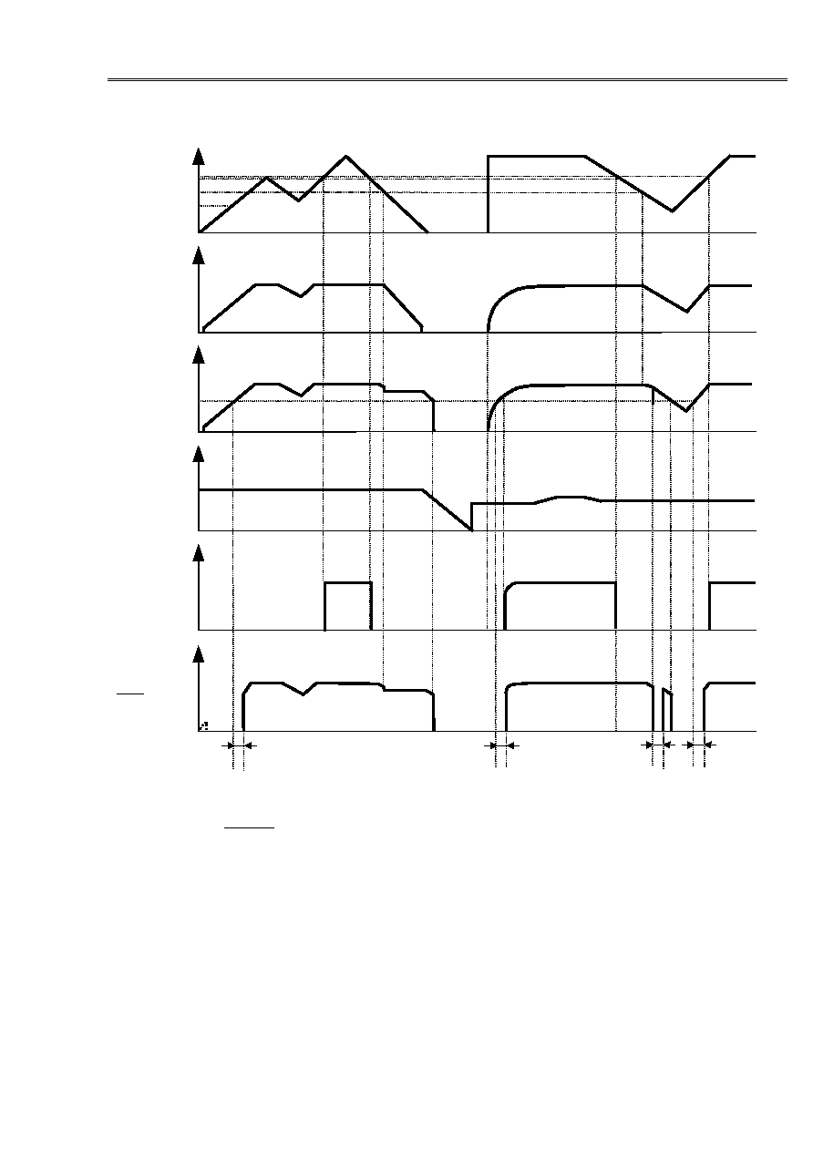
Operation Timing Chart
Remark CS and RESET are pulled up to V
OUT
. The Y-axis is an arbitrary scale.
Figure 4 Operation Timing Chart
V
BAT
(V)
V
CS
(V)
V
OUT
(V)
V
RO,
V
CH
(V)
V
IN
(V)
V
RESET
(V)
t
DELAY
t
DELAY
t
DELAY
t
DELAY

BATTERY BACKUP SWITCHING IC
S-8425 Series
Rev.1.1
_10
Seiko Instruments Inc.
8
Operation
The internal configuration of the S-8425 Series is as follows.
· Voltage regulator 1, which stabilizes input voltage V
IN
and outputs it to V
RO
· Voltage regulator 2, which stabilizes input voltage V
IN
and outputs it to V
OUT
· Voltage regulator 3, which stabilizes input voltage V
IN
and outputs it to V
CH
· CS voltage detector, which monitors input voltage V
IN
· RESET voltage detector, which monitors output voltage V
OUT
· Switch unit
The functions and operations of the above-listed elements are described below.
1. Voltage
Regulators
The S-8425 Series features on-chip voltage regulators with a small dropout voltage. The voltage of
the VRO, VOUT, and VCH pins (the output pins of the voltage regulator) can separately be selected
for the output voltage in 0.1 V steps between the range of 2.3 to 5.4 V.
[Dropout voltage V
drop1
, V
drop2
, V
drop3
]
Assume that the voltage output from the VRO pin is V
RO(E)
under the conditions of output voltage 1
described in the electrical characteristics table. V
IN1
is defined as the input voltage at which the output
voltage from the VRO pin becomes 98% of V
RO(E)
when the input voltage V
IN
is decreased. Then, the
dropout voltage V
drop1
is calculated by the following expression.
V
drop1
= V
IN1
- V
RO(E)
× 0.98
Similarly, assume that the voltage of the VOUT pin is V
OUT(E)
, and V
CH(E)
respectively under the
conditions of output voltage 2 and 3 described in the electrical characteristics table. V
IN2
and V
IN3
are
defined as the input voltages at which the output voltage from the VOUT pin becomes 98% of V
OUT(E)
and V
CH(E)
, respectively. Then, the dropout voltages V
drop2
and V
drop3
are calculated by the following
expression.
V
drop2
= V
IN2
- V
OUT(E)
× 0.98
V
drop3
= V
IN3
- V
CH(E)
× 0.98
2. Voltage
Detector
The S-8425 Series incorporates two high-precision, low power consuming voltage detectors with
hysteresis characteristics. The power of the CS voltage detector is supplied from the VIN and VBAT
pins. Therefore, the output is stable as long as the primary or backup power supply is within the
operating voltage range (1.7 to 16 V). All outputs are Nch open-drain, and need pull-up resistors of
about 100 k
.
2.1 CS Voltage Detector
The CS voltage detector monitors the input voltage V
IN
(VIN pin voltage). The detection voltage can
be selected from between 2.4 and 5.3 V in 0.1 V steps. The result of detection is output at the CS
pin: "Low" for lower voltage than the detection level and "High" for higher voltage than the release
level (however, when the VOUT pin voltage is the CS output inhibit voltage (V
SW2
), a low level is
output).
Figure 5 Definition of Detection and Release Voltages
Release voltage
Input voltage
Output voltage
Detection voltage
BATTERY BACKUP SWITCHING IC
Rev.1.1
_10
S-8425 Series
Seiko Instruments Inc.
9
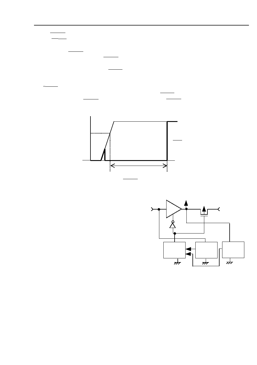
2.2 RESET Voltage Detector
The RESET voltage detector monitors the output voltage V
OUT
(VOUT pin voltage). The detection
voltage can be selected from between 1.7 V and 3.4 V in 0.1 V steps. The result of detection is
output at the RESET pin: "Low" for a lower voltage than the detection level and "High" for a higher
voltage than the release level. RESET outputs the normal logic if the VOUT pin voltage is 1.0 V or
more.
The S-8425 Series incorporates a RESET release delay circuit.
[RESET release delay time (t
DELAY
)]
The interval from when the VOUT pin voltage exceeds the RESET release voltage value (
+V
DET2
)
until the output of the RESET pin is actually inverted is called the RESET release delay time.
Figure 6 Definition of RESET Release Delay Time (t
DELAY
)
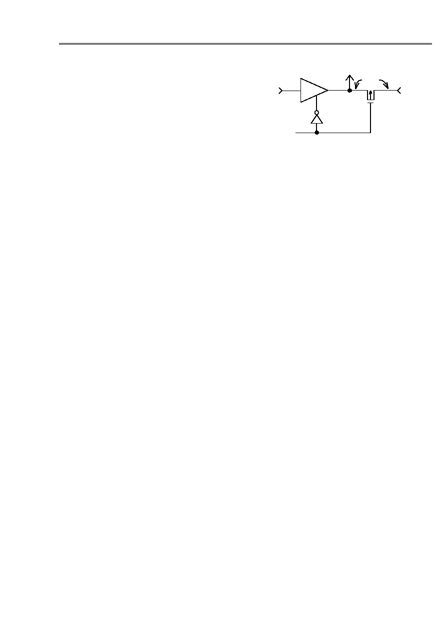
3. Switch
Unit
The switch unit consists of the V
SW1
and
V
SW2
detectors, a switch controller, voltage
regulator 2, and switch transistor M1 (see
Figure 7 Switch Unit).
3.1 V
SW1
Detector
The V
SW1
detector monitors the power
supply voltage V
IN
and sends the results of
detection to the switch controller. The
detection voltage (V
SW1
) can be set to 77
±2% or 85 ±2% of the CS release voltage
+V
DET1
.
Figure 7 Switch Unit
VOUT
M1
VBAT
VIN
Switch
controller
V
SW1
detector
V
SW2
detector
t
DELAY
+V
DET2
V
OUT
V
RESET
V
t
REG2

BATTERY BACKUP SWITCHING IC
S-8425 Series
Rev.1.1
_10
Seiko Instruments Inc.
10
3.2 V
SW2
Detector
The V
SW2
detector monitors the VOUT pin voltage and keeps the CS release voltage output low until
the VOUT pin voltage rises to V
SW2
voltage. The CS pin output then changes from low to high if the
VIN pin voltage is more than the CS release voltage (
+V
DET1
) when the VOUT pin voltage rises to 95
±2% of the output voltage of voltage regulator 2 (V
OUT
). The CS pin output changes from high to low
regardless of the V
SW2
voltage when the VIN pin voltage drops to less than the CS detection voltage
(
-V
DET1
).
The CS pin output remains high if the VIN pin voltage stays higher than the CS detection voltage
(
-V
DET1
) when the VOUT pin voltage drops to less than the V
SW2
voltage due to an undershoot.
3.3 Switch Controller
The switch controller controls voltage regulator 2 and switch transistor M1. There are two statuses
corresponding to the power supply voltage V
IN
(or power supply voltage V
BAT
) sequence: a special
sequence status and a normal sequence status. When the power supply voltage V
IN
rises and
becomes equal to or exceeds the CS release voltage (
+V
DET1
), the normal sequence status is
entered, but until then the special sequence status is maintained.
(1) Special sequence status
The switch controller sets voltage regulator 2 ON and switch transistor M1 OFF from the initial
status until the primary power supply voltage V
IN
is connected and reaches more than the CS
release voltage (
+V
DET1
) in order to prevent consumption of the backup power supply regardless
of the V
SW1
detector status. This status is called the special sequence status.
(2) Normal sequence status
The switch controller enters the normal sequence status from the special sequence status once
the primary power supply voltage V
IN
reaches more than the CS release voltage (
+V
DET1
).
Once the normal sequence is entered, the switch controller switches voltage regulator 2 and
switch transistor M1 ON/OFF as shown in Table 3 according to the power supply voltage V
IN
. The
time required for voltage regulator 2 to be switched from OFF to ON is a few hundred
µs at most.
During this interval, voltage regulator 2 and switch transistor M1 may both switch OFF and the
VOUT pin voltage may drop. To prevent this, connect a capacitor of 10
µF or more to the VOUT
pin.
When the VOUT pin voltage becomes lower than the RESET detection voltage, the status returns
to the special sequence status.
Table 3 ON/OFF Switching of Voltage Regulator 2 and Switch Transistor M1
According to Power Supply Voltage V
IN
Power Supply Voltage V
IN
Voltage Regulator 2
Switch Transistor M1
VOUT Pin Voltage
V
IN
> V
SW1
ON OFF V
OUT
V
IN
< V
SW1
OFF ON
V
BAT
- V
dif
BATTERY BACKUP SWITCHING IC
Rev.1.1
_10
S-8425 Series
Seiko Instruments Inc.
11
3.4 Switch Transistor M1
Voltage regulator 2 is also used to switch from the
VIN pin to the VOUT pin. Therefore, no reverse
current flows from the VOUT pin to the VIN pin
when voltage regulator 2 is OFF.
The output voltage of voltage regulator 2 can be
selected from between 2.3 V and 5.4 V in 0.1 V
steps.
The on-resistance of switch transistor M1 is 60
or lower (I
OUT
= 10 to 500 µA).
Therefore, when M1 is switched ON and the VOUT pin is connected to the VBAT pin, the voltage
drop V
dif
caused by M1 is 60
× I
OUT
(output current) at maximum, and V
BAT
- V
dif
(max.) is output to
the VOUT pin at minimum.
When voltage regulator 2 is ON and M1 is OFF, the leakage current of M1 is kept below 0.1
µA max.
(V
IN
= 6 V, Ta = 25°C) with the VBAT pin grounded (VSS pin).
Figure 8 Definition of V
dif
VIN
VBAT
VOUT
M1
REG2
V
dif
BATTERY BACKUP SWITCHING IC
S-8425 Series
Rev.1.1
_10
Seiko Instruments Inc.
12
Transient Response
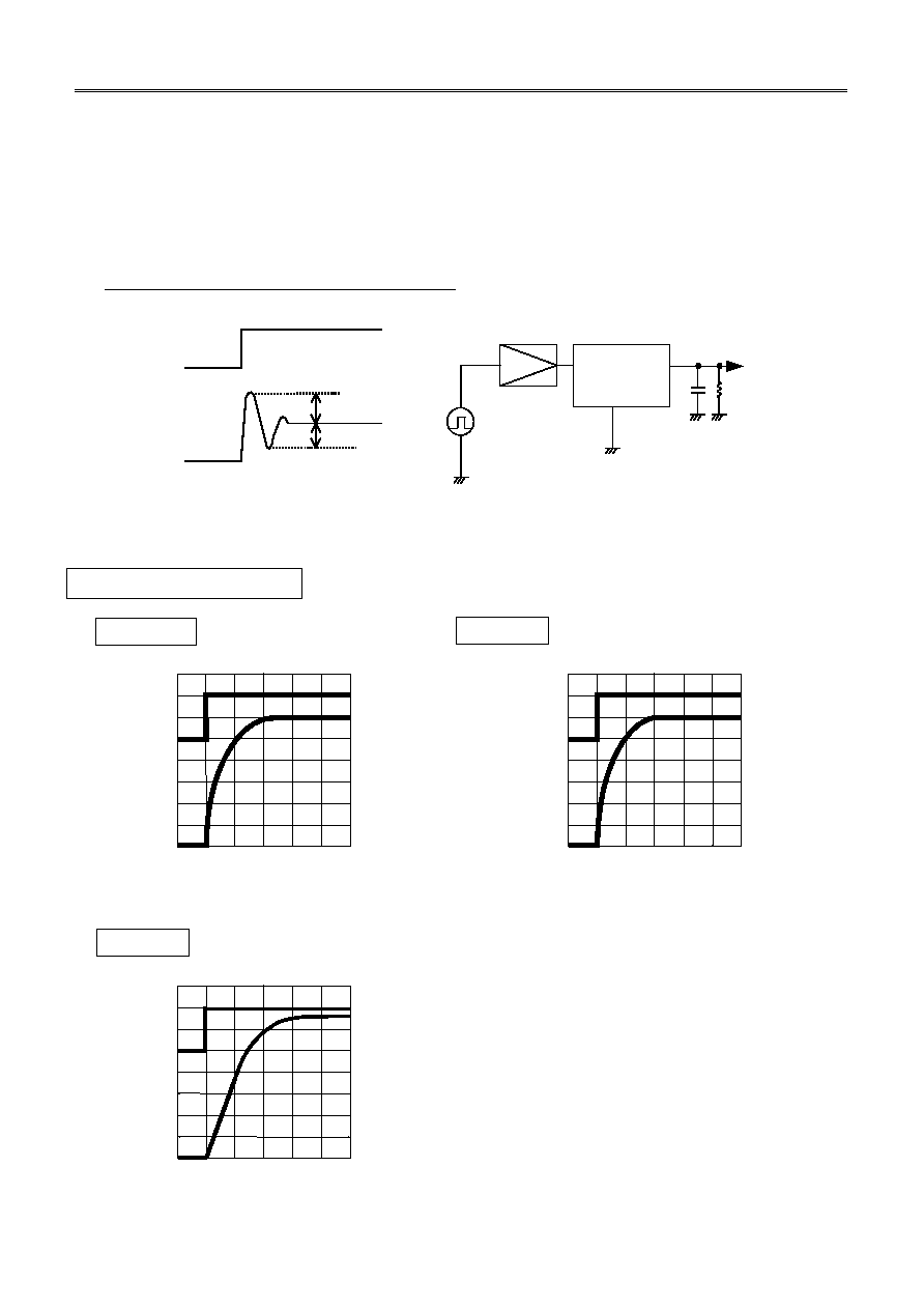
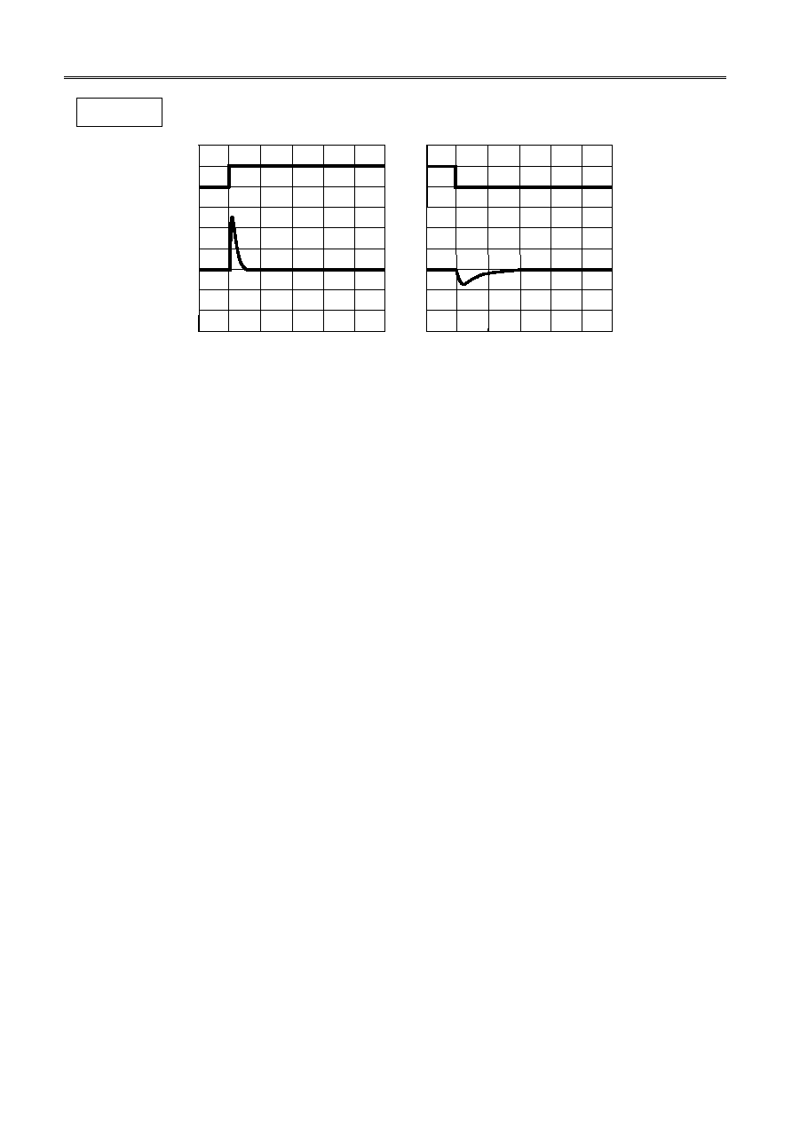
1. Line Transient Response Against Input Voltage Variation
The input voltage variation differs depending on whether the power supply input (0 V to 10 V square
wave) is applied or the power supply variation (6 V and 10 V square waves) is applied. This section
describes the ringing waveforms and parameter dependency of each type. The test circuit is shown
for reference.
Power supply application: 0 V to 10 V square wave
10 V
Output voltage
Overshoot
Undershoot
Input voltage
0 V
Fast amplifier
R
L
S-8425
Series
P.G.
VSS
VOUT
VIN
C
OUT
Oscillo-
scope
Figure 9 Power Supply Application:
0 V to 10 V Square Wave
Figure 10 Test Circuit
Power Supply Application
VOUT pin
VRO pin
C
OUT
= 22 µF, I
OUT
= 50 mA, Ta = 25°C
C
RO
= 22 µF, I
RO
= 30 mA, Ta = 25°C
t
(100
µs/div)
t
(100
µs/div)
Figure 11 Ringing Waveform of Power
Supply Application (VOUT Pin)
Figure 12 Ringing Waveform of Power
Supply Application (VRO Pin)
VCH
pin
C
CH
= 10 µF, I
CH
= 10 mA, Ta = 25°C
t
(100
µs/div)
Figure 13 Ringing Waveform of Power
Supply Application (VCH Pin)
Input voltage
(5 V/div)
Output voltage
(0.5 V/div)
Input voltage
(5 V/div)
Output voltage
(0.5 V/div)
Output voltage
(0.5 V/div)
Input voltage
(5 V/div)
10 V
10 V
10 V
0 V
0 V
0 V
BATTERY BACKUP SWITCHING IC
Rev.1.1
_10
S-8425 Series
Seiko Instruments Inc.
13
Power supply variation: 6 V and 10 V square waves
Power Supply Variation
VOUT pin
C
OUT
= 22 µF, I
OUT
= 50 mA, Ta = 25°C
t (100
µs/div)
Figure 16 Ringing Waveform of Power Supply Variation (VOUT Pin)
VRO pin
C
RO
=
=
=
= 22 µF, I
RO
=
=
=
= 30 mA, Ta ==== 25°C
t (100
µs/div)
Figure 17 Ringing Waveform of Power Supply Variation (VRO Pin)
Figure 14 Power Supply Variation:
6 V and 10 V Square Waves
Figure 15 Test Circuit
Fast amplifier
Oscillo-
scope
S-8425 Series
P.G.
VSS
VOUT
VIN
C
OUT
R
L
10 V
Overshoot
6 V
Input
voltage
Output
voltage
Undershoot
Input voltage
(4 V/div)
Output voltage
(50 mV/div)
10 V
10 V
6 V
6 V
Output voltage
(50 mV/div)
Input voltage
(4 V/div)
10 V
10 V
6 V
6 V
BATTERY BACKUP SWITCHING IC
S-8425 Series
Rev.1.1
_10
Seiko Instruments Inc.
14
VCH pin
C
CH
=
=
=
= 10 µF, I
CH
=
=
=
= 10 mA, Ta ==== 25°C
t (100
µs/div)
Figure 18 Ringing Waveform of Power Supply Variation (VCH Pin)
Output voltage
(50 mV/div)
Input voltage
(4 V/div)
6 V
6 V
10 V
10 V
BATTERY BACKUP SWITCHING IC
Rev.1.1
_10
S-8425 Series
Seiko Instruments Inc.
15
Reference data: Dependency of output current (I
OUT
), load capacitance (C
OUT
), input variation
width
(
V
IN
), temperature (Ta)
For reference, the following pages describe the results of measuring the ringing amounts at the VOUT
and VRO pins using the output current (I
OUT
), load capacitance (C
OUT
), input variation width (
V
IN
), and
temperature (Ta) as parameters.
1.1 I
OUT
Dependency
(1) VOUT pin
(2) VRO pin
C
OUT
= 22 µF, V
IN
= 6 V and 10 V, Ta = 25°C C
RO
= 22 µF, V
IN
= 6 V and 10 V, Ta = 25°C
Ring
i
ng am
oun
t
(
V
)
I
OUT
(mA)
0.00
0.05
0.10
0.15
0.20
0.25
0
20
40
60
Ring
i
ng am
oun
t
(
V
)
I
RO
(mA)
0.00
0.05
0.10
0.15
0.20
0.25
0
20
40
60
(3) VCH pin
C
CH
= 10 µF, V
IN
= 6 V and 10 V, Ta = 25°C
Ring
i
ng am
oun
t
(
V
)
I
OUT
(mA)
0.00
0.05
0.10
0.15
0.20
0.25
0
20
40
60
Overshoot
Undershoot
BATTERY BACKUP SWITCHING IC
S-8425 Series
Rev.1.1
_10
Seiko Instruments Inc.
16
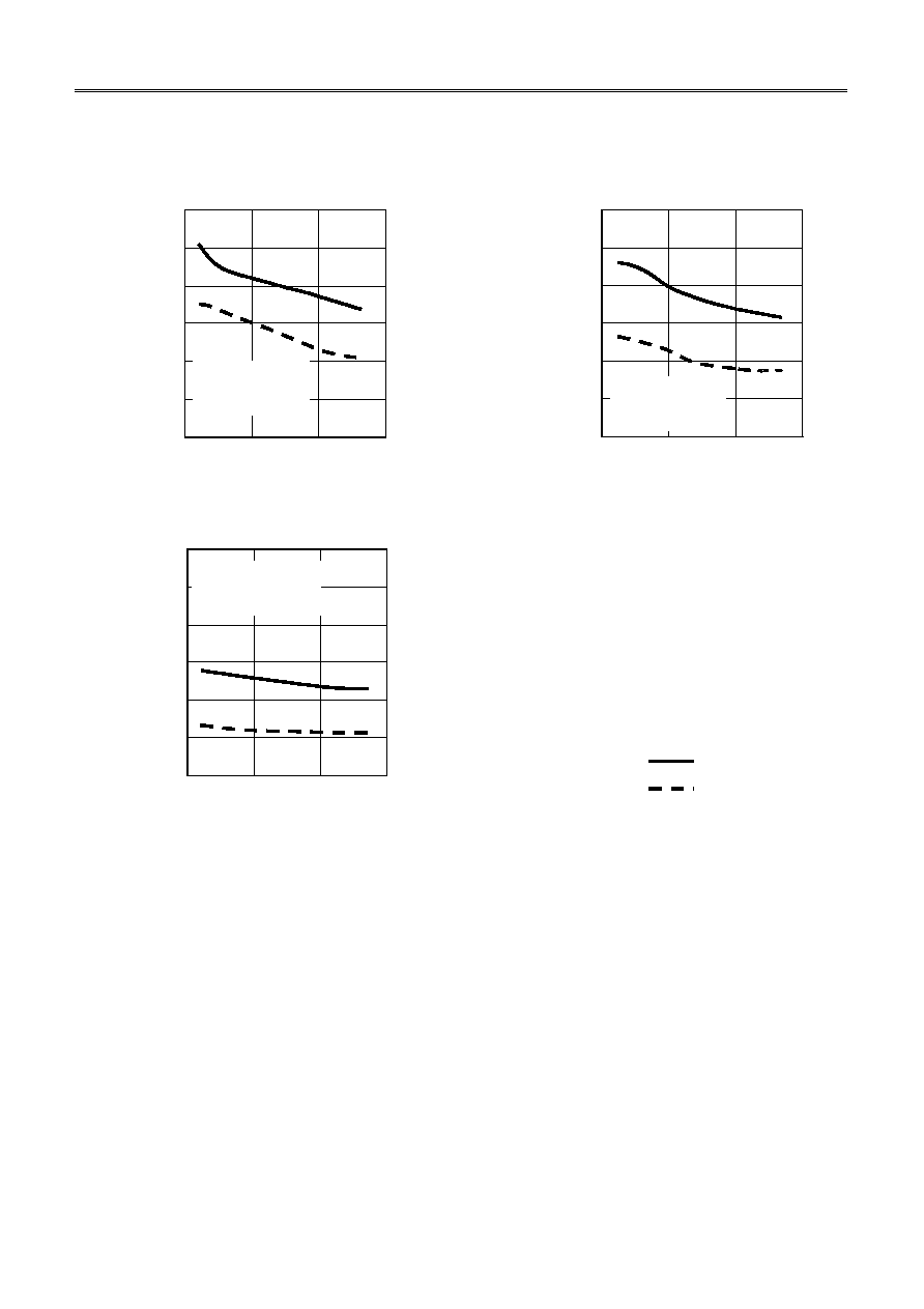
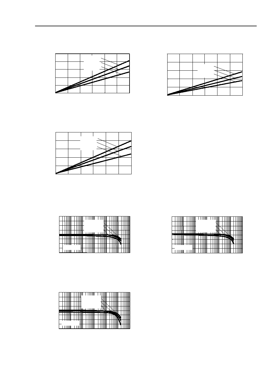
1.2 C
OUT
Dependency
(1) VOUT pin
(2) VRO pin
I
OUT
= 50 mA, V
IN
= 6 V and 10 V, Ta = 25°C I
RO
= 30 mA, V
IN
= 6 V and 10 V, Ta = 25°C
Ring
i
ng am
oun
t
(
V
)
C
OUT
(
µF)
0.00
0.10
0.20
0.30
0.40
0.50
0
10
40
50
20
30
Ring
i
ng am
oun
t
(
V
)
C
RO
(
µF)
0.00
0.10
0.20
0.30
0.40
0.50
0
10
40
50
20
30
(3) VCH pin
I
CH
= 10 mA, V
IN
= 6 V and 10 V, Ta = 25°C
Ring
i
ng am
oun
t
(
V
)
C
CH
(
µF)
0.00
0.10
0.20
0.30
0.40
0.50
0
10
40
50
20
30
Overshoot
Undershoot
BATTERY BACKUP SWITCHING IC
Rev.1.1
_10
S-8425 Series
Seiko Instruments Inc.
17
1.3
V
IN
Dependency
V
IN
shows the difference between the low voltage fixed to 6 V and the high voltage.
For example,
V
IN
= 2 V means the difference between 6 V and 8 V.
(1) VOUT pin
(2) VRO pin
I
OUT
= 50 mA, C
OUT
= 22 µF, Ta = 25°C
I
RO
= 30 mA, C
RO
= 22 µF, Ta = 25°C
V
IN
(V)
0.00
0.05
0.10
0.15
0.20
0.25
0.30
0
1
2
3
4
5
Ring
i
ng am
oun
t
(
V
)
0.00
0.05
0.10
0.15
0.20
0.25
0.30
0
1
2
3
4
5
Ring
i
ng am
oun
t
(
V
)
V
IN
(V)
(3) VCH pin
I
CH
= 10 mA, C
CH
= 10 µF, Ta = 25°C
V
IN
(V)
0.00
0.05
0.10
0.15
0.20
0.25
0.30
0
1
2
3
4
5
Ring
i
ng am
oun
t
(
V
)
Overshoot
Undershoot
BATTERY BACKUP SWITCHING IC
S-8425 Series
Rev.1.1
_10
Seiko Instruments Inc.
18
1.4
Temperature Dependency
(1) VOUT pin
(2) VRO pin
Ta (
°C)
V
IN
= 6 and 10 V
I
OUT
= 50 mA
C
OUT
= 22 µF
0.00
0.05
0.10
0.15
0.20
0.25
0.30
-50
0
50
100
Ring
i
ng am
oun
t
(
V
)
(3) VCH pin
Ta (
°C)
0.00
0.05
0.10
0.15
0.20
0.25
0.30
-50
0
50
100
Ring
i
ng am
oun
t
(
V
)
V
IN
= 6 V and 10 V
I
CH
= 10 mA
C
CH
= 10 µF
Overshoot
Undershoot
Ta (
°C)
V
IN
= 6 and 10 V
I
RO
= 30 mA
C
RO
= 22 µF
0.00
0.05
0.10
0.15
0.20
0.25
0.30
-50
0
50
100
Ring
i
ng am
oun
t
(
V
)
BATTERY BACKUP SWITCHING IC
Rev.1.1
_10
S-8425 Series
Seiko Instruments Inc.
19
2. Load Transient Response Based on Output Current Fluctuation
The overshoot and undershoot are caused in the output voltage if the output current fluctuates
between 10
µA and 50 mA (V
RO
is between 10
µA and 30 mA, V
CH
is between 10
µA and 10 mA)
while the input voltage is constant. Figure 19 shows the output voltage variation due to the output
current. Figure 20 shows the test circuit for reference. The latter half of this section describes ringing
waveform and parameter dependency.
Undershoot
Overshoot
Output
current
Output
current
50 mA
10
µA
Figure 19 Output Voltage Variation
Figure 20 Test Circuit
due to Output Current
Figures 21 to 23 show the ringing waveforms at the VOUT, VRO, and VCH pins due to the load
variation.
VOUT pin
V
IN
= 6.0 V, C
OUT
= 22 µF, Ta = 25°C
t (500 ms/div)
t (50
µs/div)
Figure 21 Ringing Waveform due to Load Variation (VOUT Pin)
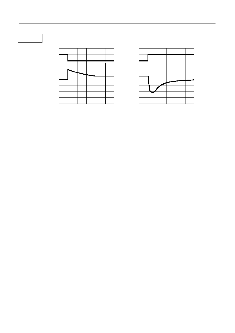
VRO pin
V
IN
= 6.0 V, C
RO
= 22 µF, Ta = 25°C
t (20 ms/div)
t (50
µs/div)
Figure 22 Ringing Waveform due to Load Variation (VRO Pi n)
Oscillo-
scope
S-8425 Series
VSS
VOUT
VIN
C
OUT
Output current
Output voltage
(50 mV/div)
10
µA
50 mA
10
µA
50 mA
Output current
Output voltage
(20 mV/div)
10
µA
30 mA
10
µA
30 mA
BATTERY BACKUP SWITCHING IC
S-8425 Series
Rev.1.1
_10
Seiko Instruments Inc.
20
VCH pin
V
IN
= 6.0 V, C
CH
= 10 µF, Ta = 25°C
t (5 ms/div)
t (50
µs/div)
Figure 23 Ringing Waveform due to Load Variation (VCH Pin)
Output current
Output voltage
(10 mV/div)
10
µA
10 mA
10
µA
10 mA
BATTERY BACKUP SWITCHING IC
Rev.1.1
_10
S-8425 Series
Seiko Instruments Inc.
21
Reference data: Dependency of input voltage (V
IN
), load capacitance (C
OUT
), output variation
width
(
I
OUT
), temperature (Ta)
2.1 V
IN
Dependency
(1) VOUT pin
(2) VRO pin
C
OUT
= 22 µF, I
OUT
= 50 mA and 10 µA, Ta = 25°C C
RO
= 22 µF, I
RO
= 30 mA and 10 µA, Ta = 25°C
Ring
i
ng am
oun
t
(
V
)
V
IN
(V)
0.00
0.04
0.06
0.08
0.10
0.12
4
5
8
10
6
7
0.02
9
Ring
i
ng am
oun
t
(
V
)
V
IN
(V)
0.00
0.04
0.06
0.08
0.10
0.12
4
5
8
10
6
7
0.02
9
(3) VCH pin
C
CH
= 10 µF, I
CH
= 10 mA and 10 µA, Ta = 25°C
Ring
i
ng am
oun
t
(
V
)
V
IN
(V)
0.00
0.04
0.06
0.08
0.10
0.12
4
5
8
10
6
7
0.02
9
Overshoot
Undershoot
BATTERY BACKUP SWITCHING IC
S-8425 Series
Rev.1.1
_10
Seiko Instruments Inc.
22
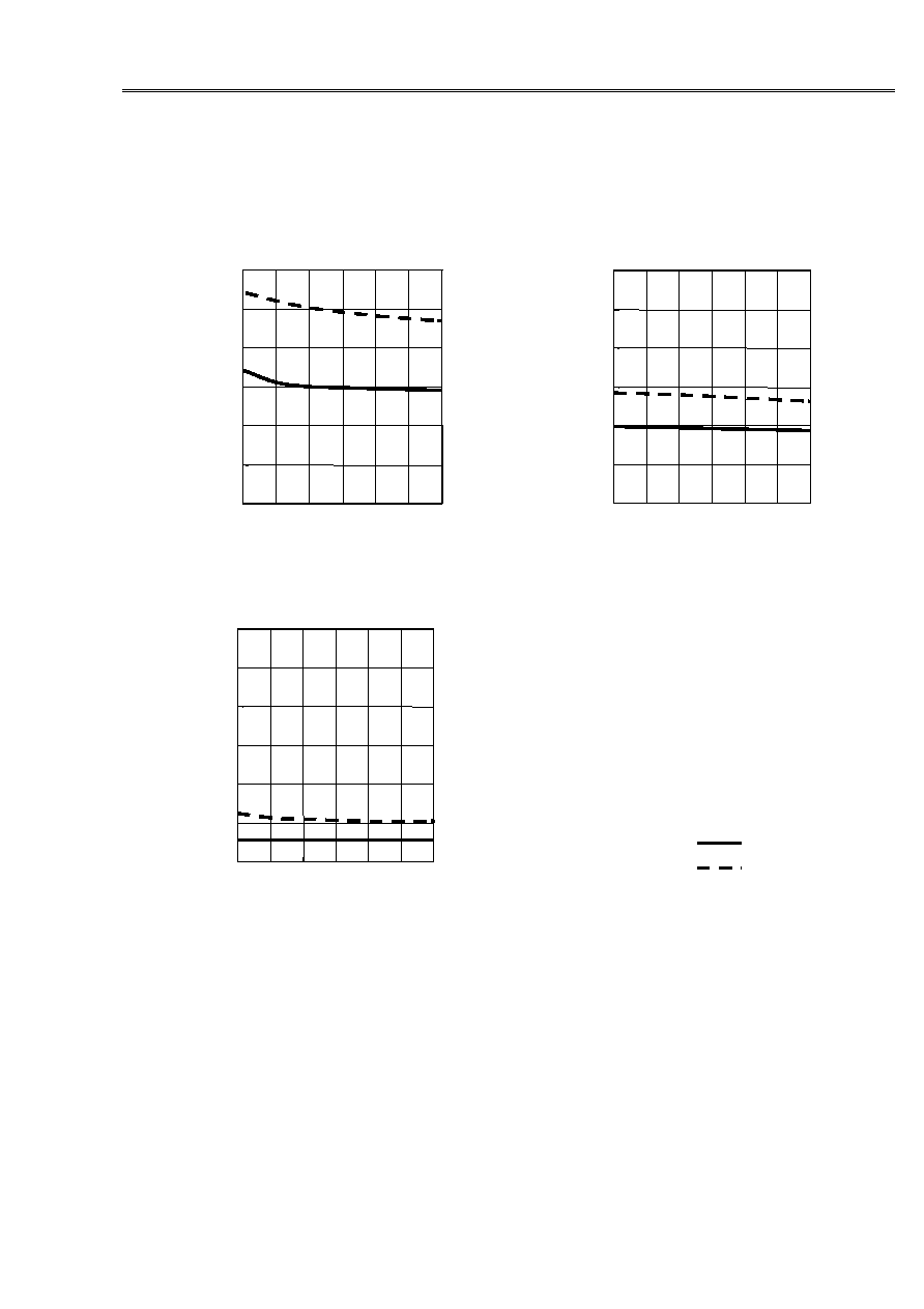
2.2 C
OUT
Dependency
(1) VOUT pin
(2) VRO pin
V
IN
= 6.0 V, I
OUT
= 50 mA and 10 µA, Ta = 25°C V
IN
= 6.0 V, I
RO
= 30 mA and 10 µA, Ta = 25°C
Ring
i
ng am
oun
t
(
V
)
C
OUT
(
µF)
0.00
0.20
0.30
0.40
0.50
0.60
0
10
40
50
20
30
0.10
Ring
i
ng am
oun
t
(
V
)
C
RO
(
µF)
0.00
0.10
0.15
0.20
0.25
0.30
0
10
40
50
20
30
0.05
(3) VCH pin
C
CH
= 10 µF, I
CH
= 10 mA and 10 µA, Ta = 25°C
Ring
i
ng am
oun
t
(
V
)
C
CH
(
µF)
0.00
0.20
0.30
0.40
0.50
0.60
0
10
40
50
20
30
0.10
Overshoot
Undershoot
BATTERY BACKUP SWITCHING IC
Rev.1.1
_10
S-8425 Series
Seiko Instruments Inc.
23
2.3
I
OUT
Dependency
I
OUT
and
I
RO
show the fluctuation between the low current stabilized at 10
µA and the high current.
For example,
I
OUT
= 10 mA means a fluctuation between 10 µA and 10 mA.
(1) VOUT pin
(2) VRO pin
C
OUT
= 22 µF, V
IN
= 6 V, Ta = 25°C
C
RO
= 22 µF, V
IN
= 6 V, Ta = 25°C
I
OUT
(mA)
Ring
i
ng am
oun
t
(
V
)
0.00
0.02
0.04
0.06
0.08
0.10
0.12
0 10 20 30 40 50 60
0.00
0.02
0.04
0.06
0.08
0.10
0.12
0 10 20 30 40 50 60
Ring
i
ng am
oun
t
(
V
)
I
RO
(mA)
(3) VCH pin
C
CH
= 10 µF, V
IN
= 6 V, Ta = 25°C
I
CH
(mA)
Ring
i
ng am
oun
t
(
V
)
0.00
0.02
0.04
0.06
0.08
0.10
0.12
0 10 20 30 40 50 60
Overshoot
Undershoot
BATTERY BACKUP SWITCHING IC
S-8425 Series
Rev.1.1
_10
Seiko Instruments Inc.
24
2.4 Temperature Dependency
(1) VOUT pin
(2) VRO pin
V
IN
= 6.0 V, I
OUT
= 50 µA and 10 µA, C
OUT
= 22 µF
V
IN
= 6.0 V, I
RO
= 30 mA and 10 µA, C
RO
= 22 µF
Ring
i
ng am
oun
t
(
V
)
0.00
0.02
0.04
0.06
0.08
0.10
0.12
0.14
0.16
-50
0
50
100
Ta (
°C)
Ring
i
ng am
oun
t
(
V
)
0.00
0.01
0.02
0.03
0.04
0.05
0.06
0.07
0.08
-50
0
50
100
Ta (
°C)
(3) VCH pin
V
IN
= 6 V, I
CH
= 10 mA and 10 µA, C
CH
= 10 µF
Ring
i
ng am
oun
t
(
V
)
0.00
0.02
0.04
0.06
0.08
0.10
0.12
0.14
0.16
-50
0
50
100
Ta (
°C)
Overshoot
Undershoot
BATTERY BACKUP SWITCHING IC
Rev.1.1
_10
S-8425 Series
Seiko Instruments Inc.
25
Standard Circuit
VRO
V
RO
10
µF
V
OUT
RESET
CS
VSS
6 V
3 V
VIN
VBAT
VOUT
10
µF
S-8425
Series
0.1
µF
+
+
+
1 k
10
µF
V
OUT
100 k
100 k
V
CH
10
µF
+
VCH
V
OUT
Figure 24 Standard Circuit
Caution
·
·
·
· Be sure to add a 10 µµµµF or more capacitor to the VOUT, VRO, and VCH pins.
·
·
·
· The above connections and values will not guarantee correct operation.
Before setting these values, perform sufficient evaluation on the
application to be actually used.
Package Power Dissipation
Figure 25 Power Dissipation
125
100
200
300
400
25
50
75
Ambient temperature Ta (
°C)
100
Pow
e
r
dis
s
i
pation P
D
(m
W
)
Not mounted
8-Pin TSSOP
8-Pin SON(B)
0
150
BATTERY BACKUP SWITCHING IC
S-8425 Series
Rev.1.1
_10
Seiko Instruments Inc.
26
Precautions
· In applications in which any one of I
RO
, I
OUT
, or I
CH
is small, the output voltages V
RO
,
V
OUT
, and V
CH
may rise, causing the load stability to exceed standard levels. Set I
RO
, I
OUT
, or I
CH
to 10
µA or
more.
· Attach the proper capacitor to the VOUT pin to prevent the RESET voltage detector (which
monitors the VOUT pin) from becoming active due to undershoot.
· Watch for overshoot and ensure it does not exceed the ratings of the IC chips and/or capacitors
attached to the VRO, VOUT, and VCH pins.
· Add a 10 µF or more capacitor to the VOUT, VRO, and VCH pins.
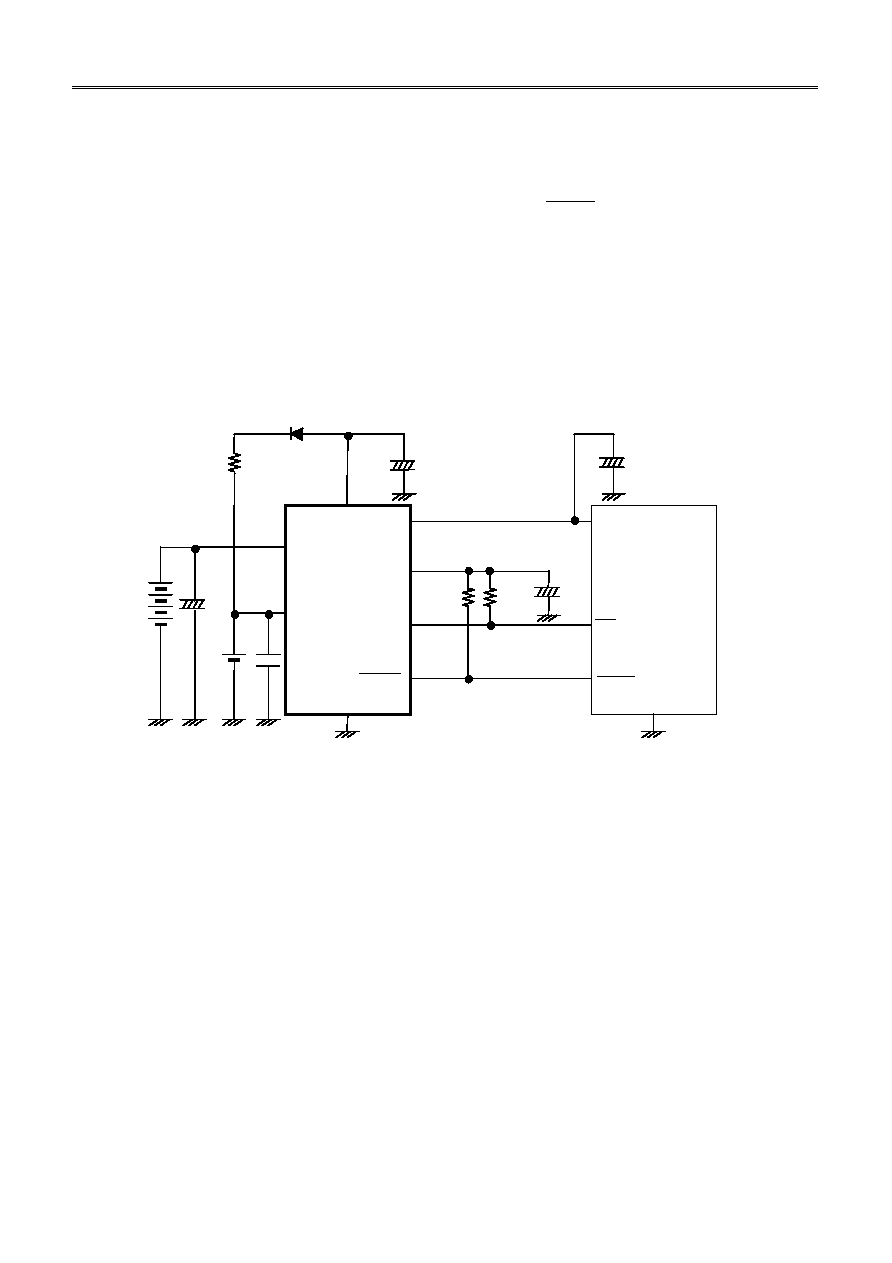
Application Circuits
When Using Secondary Battery as Backup Battery
VCH
10
µ
F
RESET
CS
VSS
6 V
VIN
VBAT
VRO
S-8425
Series
+
+
3 V
0.1
µ
F
VCC
INT
Microcontroller
10
µ
F
+
100 k
100 k
RESET
VOUT
10
µ
F
+
10
µ
F
Caution The above connection diagram and constant will not guarantee successful
operation. Perform thorough evaluation using the actual application to set
the constant.
Remark
The backup battery can be floating-recharged by using voltage regulator 3.
Figure 26 Application Circuit

BATTERY BACKUP SWITCHING IC
Rev.1.1
_10
S-8425 Series
Seiko Instruments Inc.
27
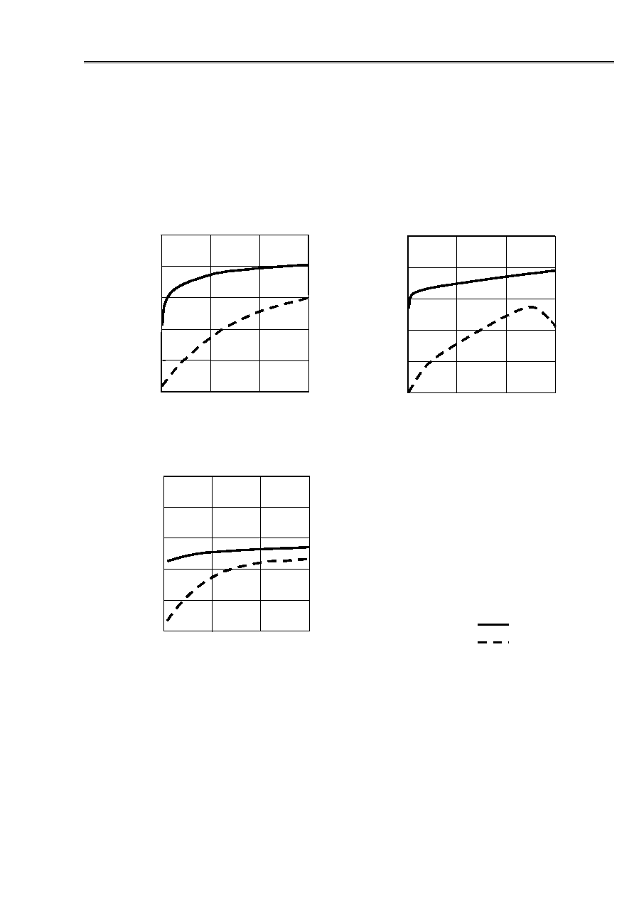
Characteristics
1. Voltage Regulator Unit
1.1 Input Voltage (V
IN
) vs. Output Voltage (V
RO
) Characteristics (REG1) (V
RO
=
=
=
= 3.0 V)
(1) Ta
=
=
=
= 85°C (2)
Ta
=
=
=
=
25
°C
I
RO
=
=
=
= 10 mA, 30 mA, 50 mA, 70 mA, 90 mA
I
RO
=
=
=
= 10 mA, 30 mA, 50 mA, 70 mA, 90 mA
2.0
2.4
2.8
3.2
2.0
3.0
4.0
5.0
V
IN
(V)
V
RO
(V)
2.0
2.4
2.8
3.2
2.0
3.0
4.0
5.0
V
IN
(V)
V
RO
(V
)
(3) Ta
=
=
=
= -40°C
I
RO
= 10 mA, 30 mA, 50 mA, 70 mA, 90 mA
2.0
2.4
2.8
3.2
2.0
3.0
4.0
5.0
V
IN
(V)
V
RO
(V)
1.2 Input Voltage (V
IN
) vs. Output Voltage (V
OUT
) Characteristics (REG2) (V
OUT
=
=
=
= 3.0 V )
(1) Ta
=
=
=
= 85°C (2)
Ta
=
=
=
= 25°C
I
OUT
=
=
=
= 10 mA, 30 mA, 50 mA, 70 mA, 90 mA
I
OUT
=
=
=
= 10 mA, 30 mA, 50 mA, 70 mA, 90 mA
2.0
2.4
2.8
3.2
2.0
3.0
4.0
5.0
V
IN
(V)
V
OU
T
(V
)
2.0
2.4
2.8
3.2
2.0
3.0
4.0
5.0
V
IN
(V)
V
OU
T
(V
)
(3) Ta
=
=
=
= -40°C
I
OUT
=
=
=
= 10 mA, 30 mA, 50 mA, 70 mA, 90 mA
2.0
2.4
2.8
3.2
2.0
3.0
4.0
5.0
V
IN
(V)
V
OUT
(V)
I
RO
= 10 mA
I
RO
= 90 mA
I
RO
= 10 mA
I
RO
= 90 mA
I
RO
= 10 mA
I
RO
= 90 mA
I
OUT
= 10 mA
I
OUT
= 90 mA
I
OUT
= 10 mA
I
OUT
= 90 mA
I
OUT
= 90 mA
I
OUT
= 10 mA
BATTERY BACKUP SWITCHING IC
S-8425 Series
Rev.1.1
_10
Seiko Instruments Inc.
28
1.3 Input Voltage (V
IN
) vs. Output Voltage (V
OUT
) Characteristics (REG3) (V
CH
=
=
=
= 3.3 V)
(1) Ta
=
=
=
= 85°C (2)
Ta
=
=
=
= 25°C
I
RO
=
=
=
= 10 mA, 30 mA, 50 mA, 70 mA
I
RO
=
=
=
= 10 mA, 30 mA, 50 mA, 70 mA
2.3
2.7
3.1
3.5
2.0
3.0
4.0
5.0
V
IN
(V)
V
CH
(V)
6.0
7.0
2.3
2.7
3.1
3.5
2.0
3.0
4.0
5.0
V
IN
(V)
V
CH
(V)
6.0
7.0
(3) Ta
=
=
=
= -40°C
I
RO
=
=
=
= 10 mA, 30 mA, 50 mA, 70 mA
2.3
2.7
3.1
3.5
2.0
3.0
4.0
5.0
V
IN
(V)
V
CH
(V)
6.0
7.0
I
CH
= 70 mA
I
CH
= 10 mA
I
CH
= 70 mA
I
CH
= 10 mA
I
CH
= 70 mA
I
CH
= 10 mA
BATTERY BACKUP SWITCHING IC
Rev.1.1
_10
S-8425 Series
Seiko Instruments Inc.
29
1.4 Output Current (I
RO
) vs. Dropout Voltage
(V
drop1
) Characteristics
1.5 Output Current (I
OUT
) vs. Dropout Voltage
(V
drop2
) Characteristics
0.0
0.2
0.4
0.6
0.8
1.0
0
0.02
0.04
0.06
I
RO
(A)
Ta
= 85°C
25
°C
- 40°C
V
drop1
(V)
0.0
0.2
0.4
0.6
0.8
1.0
0
0.02
0.04
0.06
I
OUT
(A)
V
drop2
(V)
Ta = 85
°C
25
°C
-40°C
1.6 Output Current (I
CH
) vs. Dropout Voltage
(V
drop3
) Characteristics
0.0
0.4
0.8
1.2
1.6
2.0
0
0.02
0.04
0.06
I
CH
(A)
V
drop3
(V)
Ta = 85
°C
25
°C
-40°C
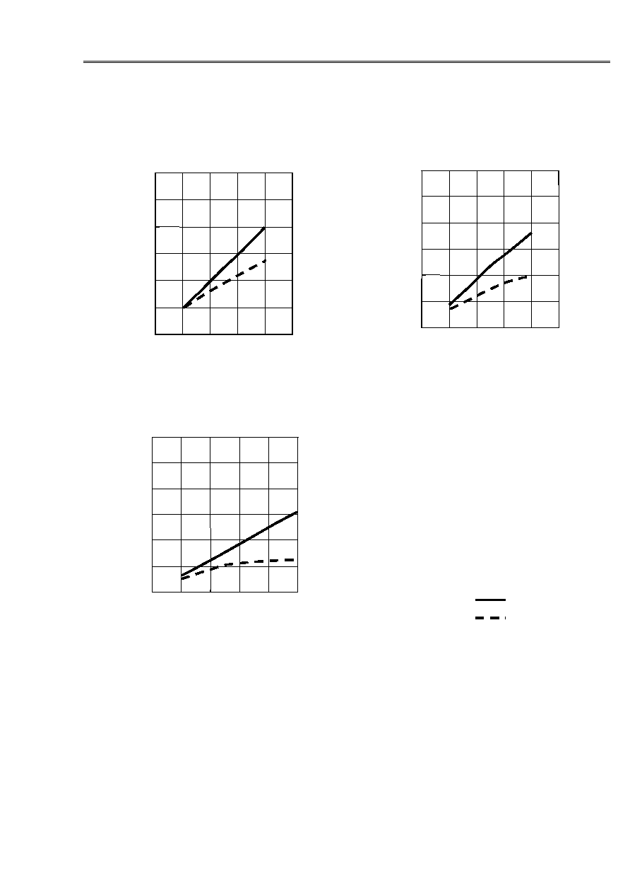
1.7 Output Current (I
RO
) vs. Output Voltage
(V
RO
) Characteristics
1.8 Output Current (I
OUT
) vs. Output Voltage
(V
OUT
) Characteristics
2.8
2.9
3.0
3.1
3.2
1 µ
100 µ
10 m
1
I
RO
(A)
V
RO
(V
)
Ta
= -40°C
25
°C
85
°C
V
IN
= 6 V
2.8
2.9
3.0
3.1
3.2
1 µ
100 µ
10 m
1
I
OUT
(A)
V
OU
T
(V
)
Ta
= -40°C
25
°C
85
°C
V
IN
= 6 V
1.9 Output Current (I
OUT
) vs. Output Voltage
(V
CH
) Characteristics
2.8
2.9
3.0
3.1
3.2
1 µ
100 µ
10 m
1
I
CH
(A)
V
CH
(V
)
Ta
= -40°C
25
°C
85
°C
V
IN
= 6 V
BATTERY BACKUP SWITCHING IC
S-8425 Series
Rev.1.1
_10
Seiko Instruments Inc.
30
1.10 Output Voltage (V
RO
) Temperature
Characteristics
1.11 Output Voltage (V
OUT
) Temperature
Characteristics
-30
-10
-20
0
30
20
10
-40
-20
0
20
40
60
80
100
Ta (
°C)
V
RO
(m
V
)
V
IN
= 6 V, I
RO
= 30 mA
Based on V
RO
voltage when Ta is 25
°C
-30
-10
-20
0
30
20
10
-40
-20
0
20
40
60
80
100
Ta (
°C)
V
OU
T
(m
V
)
V
IN
= 6 V, I
OUT
= 50 mA
Based on V
OUT
voltage when Ta is 25
°C
1.12 Output Voltage (V
CH
) Temperature
Characteristics
-30
-10
-20
0
30
20
10
-40
-20
0
20
40
60
80
100
Ta (
°C)
V
CH
(m
V
)
V
IN
= 6 V, I
CH
= 10 mA
Based on V
CH
voltage when Ta is 25
°C
1.13 Input Stability (
V
RO2
) Temperature
Characteristics
1.14 Input Stability (
V
OUT2
) Temperature
Characteristics
0
15
10
5
20
Ta (
°C)
V
RO
2
(m
V
)
-40
-20
0
20
40
80
60
100
0
15
10
5
20
Ta (
°C)
V
OU
T2
(m
V
)
-40
-20
0
20
40
80
60
100
1.15 Input Stability (
V
CH2
) Temperature
Characteristics
0
15
10
5
20
Ta (
°C)
V
CH2
(m
V
)
-40
-20
0
20
40
80
60
100

BATTERY BACKUP SWITCHING IC
Rev.1.1
_10
S-8425 Series
Seiko Instruments Inc.
31
1.16 Load Stability (
V
RO1
) Temperature
Characteristics
1.17 Load Stability (
V
OUT1
) Temperature
Characteristics
Ta (
°C)
0
10
20
30
40
V
RO
1
(m
V
)
-40
-20
0
20
40
80
60
100
Ta (
°C)
0
10
20
30
40
V
OU
T1
(m
V
)
-40
-20
0
20
40
80
60
100
1.18 Load Stability (
V
CH1
) Temperature
Characteristics
Ta (
°C)
0
10
20
30
40
V
CH1
(m
V
)
-40
-20
0
20
40
80
60
100
BATTERY BACKUP SWITCHING IC
S-8425 Series
Rev.1.1
_10
Seiko Instruments Inc.
32
2. Voltage Detector
2.1 CS Voltage Detector (
-
-
-
-V
DET1
=
=
=
= 3.3 V)
(1) Detection voltage (
-V
DET1
) temperature
characteristics
(2) Output current (I
SINK
) characteristics
-20
-10
0
10
20
Ta (
°C)
-40 -20
0
20
40
80
60
100
Based on CS (-V
DET1
) voltage when Ta is 25
°C)
CS
(
m
V
)
0
5
10
15
20
25
30
0.0
1.0
2.0
3.0
4.0
V
DS
(V)
V
IN
= 3 V
V
IN
= 1.7 V
Ta
=
25
°C
CS
I
SI
N
K
(m
A
)
(3) Output current (I
SINK
) temperature
characteristics
0
4
8
Ta (
°C)
-40 -20
0
20
40
80
60
100
2
6
10
V
IN
= V
BAT
= 2.0 V, V
DS
= 0.5 V
CS
I
SI
N
K
(m
A
)
2.2 RESET Voltage Detector (
-
-
-
-V
DET2
=
=
=
= 2.4 V)
(1) Detection voltage (
-V
DET2
) temperature
characteristics
(2) Output current (I
SINK
) characteristics
-20
-10
0
10
20
Ta (
°C)
-40 -20
0
20
40
80
60
100
Based on RESET (
-V
DET2
) voltage
when Ta is 25
°C
RE
SE
T
(
m
V
)
0
5
10
15
20
25
30
0.0
1.0
2.0
3.0
4.0
V
DS
(V)
V
IN
=
1.7 V
V
IN
=
3 V
Ta = 25°C
RE
SE
T
I
SI
N
K
(m
A
)
(3) Output current (I
SINK
) temperature
characteristics
(4) RESET release delay time
0
2
4
6
8
10
RE
S
E
T
I
SI
N
K
(m
A
)
Ta (
°C)
-40 -20
0
20
40
80
60
100
V
IN
= V
BAT
= 2.0 V, V
DS
= 0.5 V
0
1
2
3
4
5
6
Ta (
°C)
-40 -20
0
20
40
80
60
100
D
e
la
y
ti
m
e
(
m
s)
Worst
Typ
BATTERY BACKUP SWITCHING IC
Rev.1.1
_10
S-8425 Series
Seiko Instruments Inc.
33
3. Switch Unit
3.1 Switch Voltage (V
SW1
) Temperature
Characteristics
3.2 CS Output Inhibit Voltage (V
SW2
)
Temperature Characteristics
V
SW
1
(m
V
)
Ta (
°C)
-40
-20
0
20
40
80
60
100
-20
-10
0
10
20
Based on V
SW1
voltage when Ta is 25°C
Ta (
°C)
-40
-20
0
20
40
80
60
100
-20
-10
0
10
20
Based on V
SW2
voltage when Ta is 25
°C
V
SW
2
(m
V
)
3.3 Input Voltage (V
BAT
) vs. V
BAT
Switch
Resistance (R
SW
) Characteristics
3.4 V
BAT
Switch Resistance (R
SW
) Temperature
Characteristics
0
10
20
30
40
50
60
1
2
3
4
5
V
BAT
(V)
I
OUT
= 500 µA
R
SW
(
)
Ta (
°C)
-40 -20
0
20
40
80
60
100
0
10
20
30
40
50
60
V
BAT
= 3 V, I
OUT
= 500 µA
R
SW
(
)
3.5 V
BAT
Switch Leakage Current (I
LEAK
)
Temperature Characteristics
0
10
20
30
Ta (
°C)
-40 -20
0
20
40
80
60
100
5
15
25
V
IN
= 6.0 V, I
BAT
= 0 V
I
L
EAK
(n
A
)
BATTERY BACKUP SWITCHING IC
S-8425 Series
Rev.1.1
_10
Seiko Instruments Inc.
34
4. Current Consumption
4.1 V
IN
vs. V
IN
Current Consumption (I
SS1
)
Characteristics
4.2 V
BAT
vs. V
BAT2
Current Consumption (I
BAT2
)
Characteristics
Ta = 85°C
25
°C
-40°C
0
4
8
12
16
0
2
4
6
8
10
12 14
16
18
V
IN
(V)
I
SS1
(
µ
A)
0.0
0.5
1.0
1.5
2.0
2.0
2.4
2.8
3.2
3.6
4.0
V
BAT
(V)
Ta = 85°C
25
°C
-40°C
I
BAT
2
(
µ
A)
4.3 Current Consumption Temperature
Characteristics
(1) I
SS1
(2)
I
BAT2
0
4
8
12
16
Ta (
°C)
-40 -20
0
20
40
80
60
100
V
IN
= 6.0 V, V
BAT
= 3.0 V
I
SS1
(
µ
A)
0.0
0.5
1.0
1.5
2.0
Ta (
°C)
-40
-20
0
20
40
80
60
100
V
IN
= open, V
BAT
= 3.0 V
I
BAT
2
(
µ
A)
No.
TITLE
SCALE
UNIT
mm
Seiko Instruments Inc.
0.17±0.05
3.00
+0.3
-0.2
0.65
0.2±0.1
1
4
5
8
TSSOP8-A-PKG Dimensions
No. FT008-A-P-SD-1.1
FT008-A-P-SD-1.1
No.
TITLE
SCALE
UNIT
mm
Seiko Instruments Inc.
1.55±0.05
2.0±0.05
8.0±0.1
1.55
+0.1
-0
(6.9)
4.0
+0.4
-0.2
6.6
1.4±0.1
0.3±0.05
7° max.
1
4
5
8
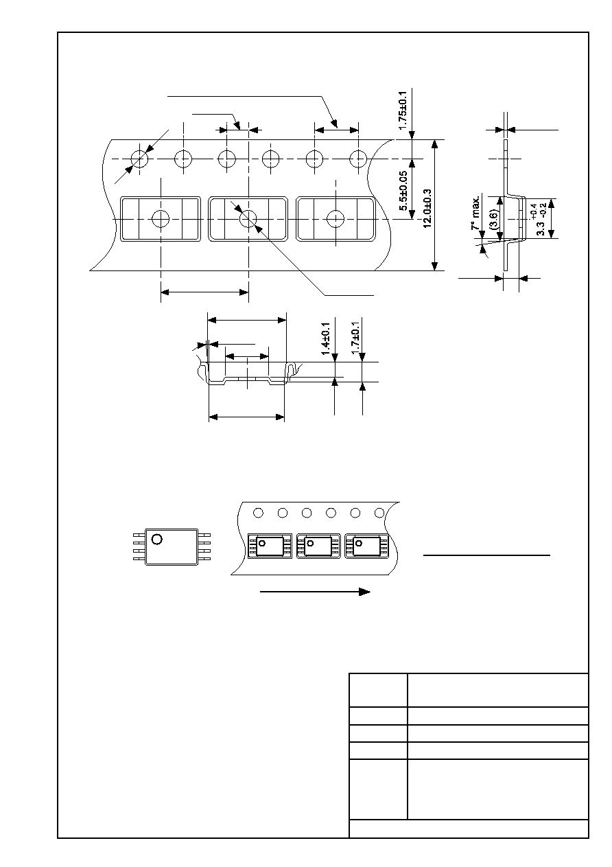
4.0±0.1(50 pitches:200.0±0.3)
Feed direction
TSSOP8-A-Carrier Tape
No. FT008-A-C-SD-3.1
FT008-A-C-SD-3.1
No.
TITLE
SCALE
UNIT
mm
Seiko Instruments Inc.
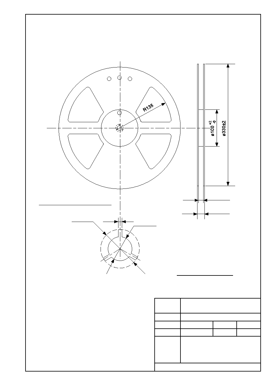
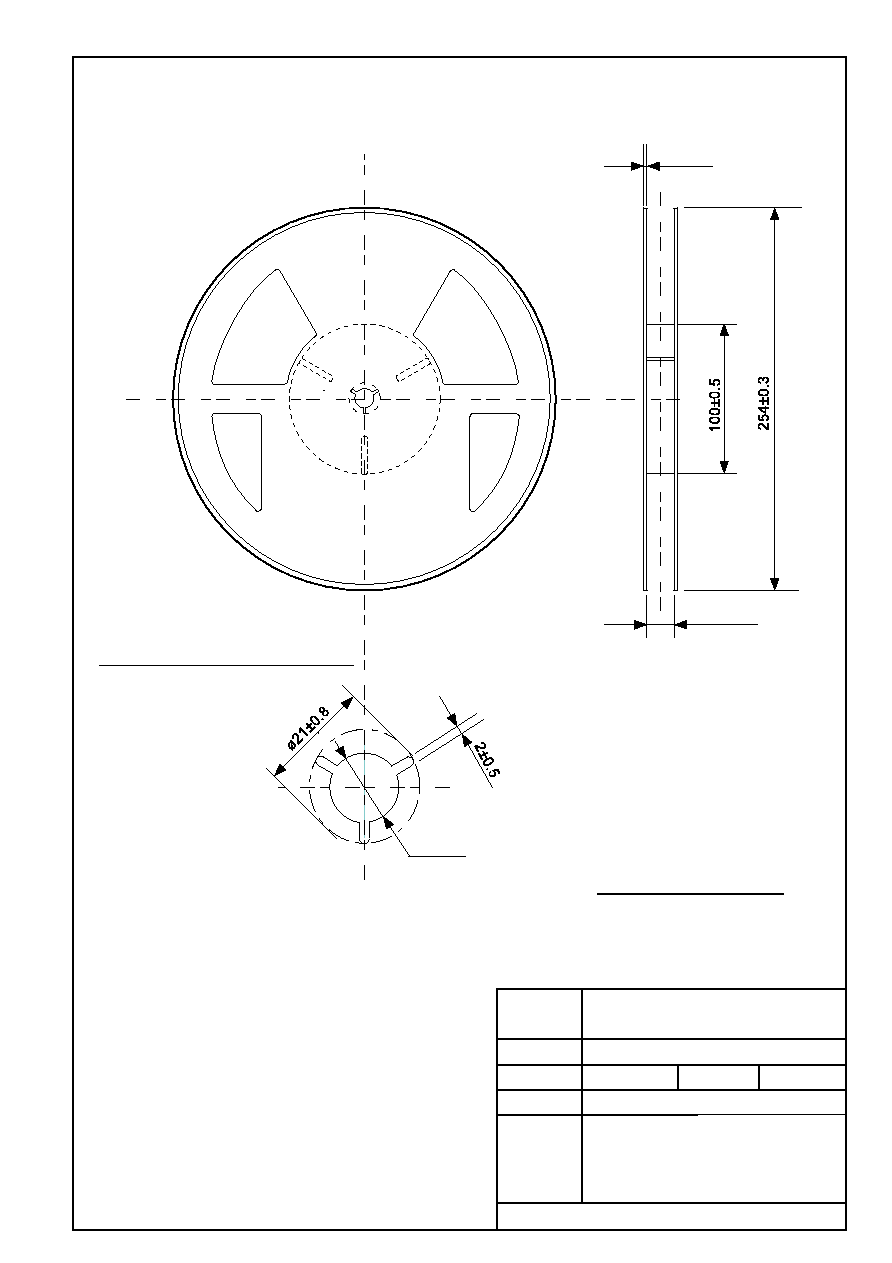
13.4±1.0
17.5±1.0
ø13±0.5
2±0.5
ø21±0.8
QTY.
3,000
Enlarged drawing in the central part
TSSOP8-A-Reel
No. FT008-A-R-SD-3.1
FT008-A-R-SD-3.1
No.
TITLE
SCALE
UNIT
mm
3.00±0.2
0.30
0.65
(2.4)
(ø1.0)
0.525typ.
+0.1
-0.05
Seiko Instruments Inc.
No. PA008-B-P-SD-1.1
PA008-B-P-SD-1.1
SON8B-B-PKG Dimensions
ø1.55±0.05
ø1.55±0.05
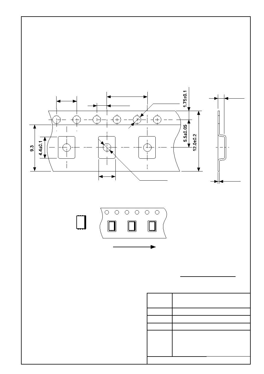
2.0±0.05
4.0±0.1
3.4±0.1
8.0±0.1
0.3±0.05
1.2±0.1
No.
TITLE
SCALE
UNIT
mm
1
4
5
8
Seiko Instruments Inc.
No. PA008-B-C-SD-1.1
PA008-B-C-SD-1.1
SON8B-B-Carrier Tape
Feed direction
2±0.3
13.5±0.5
ø13±0.2
No.
TITLE
SCALE
UNIT
mm
QTY.
3,000
Seiko Instruments Inc.
No. PA008-B-R-SD-1.1
PA008-B-R-SD-1.1
SON8B-B-Reel
Enlarged drawing in the central part

·
The information described herein is subject to change without notice.
·
Seiko Instruments Inc. is not responsible for any problems caused by circuits or diagrams described herein
whose related industrial properties, patents, or other rights belong to third parties. The application circuit
examples explain typical applications of the products, and do not guarantee the success of any specific
mass-production design.
·
When the products described herein are regulated products subject to the Wassenaar Arrangement or other
agreements, they may not be exported without authorization from the appropriate governmental authority.
·
Use of the information described herein for other purposes and/or reproduction or copying without the
express permission of Seiko Instruments Inc. is strictly prohibited.
·
The products described herein cannot be used as part of any device or equipment affecting the human
body, such as exercise equipment, medical equipment, security systems, gas equipment, or any apparatus
installed in airplanes and other vehicles, without prior written permission of Seiko Instruments Inc.
·
Although Seiko Instruments Inc. exerts the greatest possible effort to ensure high quality and reliability, the
failure or malfunction of semiconductor products may occur. The user of these products should therefore
give thorough consideration to safety design, including redundancy, fire-prevention measures, and
malfunction prevention, to prevent any accidents, fires, or community damage that may ensue.
Document Outline
- S-8425 Series
- Cover
- Features
- Package
- Applications
- Selection Guide
- Block Diagram
- Pin Assignment
- Absolute Maximum Ratings
- Electrical Characteristics
- Test Circuits
- Operation Timing Chart
- Operation
- Transient Response
- Standard Circuit
- Package Power Dissipation
- Precautions
- Application Circuits
- Characteristics
- Package Drawings