
Rev.7.4
_10
Seiko Instruments Inc.
1
S-8520/8521 Series
PWM Control & PWM/PFM Control
Step-Down Switching Regulator-Controllers
The S-8520/8521 Series consists of CMOS step-down switching regulator-
controllers with PWM-control (S-8520) and PWM/PFM-switched control (S-
8521). These devices contain a reference voltage source, oscillation circuit,
error amplifier, and other components.
The S-8520 Series provides low-ripple power, high-efficiency, and excellent
transient characteristics thanks to a PWM control circuit capable of varying
the duty ratio linearly from 0
% up to 100 %. The series also contains an
error amplifier circuit as well as a soft-start circuit that prevents overshoot at
startup.
The S-8521 Series works with either PWM control or PFM control, and can
switch from one to the other. It normally operates using PWM control with a
duty ratio of 25
% to 100 %, but under a light load, it automatically switches
to PFM control with a duty ratio of 25
%. This series ensures high efficiency
over a wide range of conditions, from standby mode to operation of
peripheral equipment.
With the addition of an external Pch Power MOS FET or PNP transistor, a coil,
capacitors, and a diode connected externally, these ICs can function as step-down
switching regulators. They serve as ideal power supply units for portable devices
when coupled with the SOT-23-5 minipackage, providing such outstanding features
as low current consumption. Since this series can accommodate an input voltage
of up to 16 V, it is also ideal when operating via an AC adapter.
Features:
Applications:
∑ Low current consumption:
In operation: 60
µA max. (A & B Series)
21
µA max. (C & D Series)
100
µA max. (E & F Series)
When powered off: 0.5
µA max.
∑ Input voltage:
2.5 V to 16 V (B, D, F Series)
2.5 V to 10 V (A, C, E Series)
∑ Output voltage:
Selectable between 1.5 V and
6.0 V in 0.1 V step
∑ Duty ratio:
0
% to 100 % PWM control (S-8520)
25
% to 100 % PWM/PFM-switched control (S-8521)
∑ The only peripheral components that can be used with this IC are a Pch power MOS FET or PNP transistor,
a coil, a diode, and capacitors (If a PNP transistor is used, a base resistance and a capacitor will also be
required).
∑ Oscillation frequency: 180 kHz typ. (A & B Series), 60 kHz typ. (C & D Series), or 300 kHz typ. (E, F Series).
∑ Soft-start function: 8 ms. typ. (A & B Series) 12 ms. typ.(C & D Series), or 4.5 ms. typ. (E, F Series).
∑ With a power-off function.
∑ With a built-in overload protection circuit. Overload detection time: 4 ms. typ. (A Series), 14 ms. typ. (C
Series) or 2.6 ms. typ.(E Series).
∑ On-board power supplies of battery devices for
portable telephones, electronic notebooks, PDAs,
and the like.
∑ Power supplies for audio equipment, including
portable CD players and headphone stereo
equipment.
∑ Fixed voltage power supply for cameras, video
equipment and communications equipment.
∑ Power supplies for microcomputers.
∑ Conversion from four NiH or NiCd cells or two
lithium-ion cells to 3.3 V/3 V.
∑ Conversion of AC adapter input to 5 V/3 V.

PWM Control & PWM/PFM Control Step-Down Switching Regulator-Controllers
S-8520/8521 Series
Rev.7.4
_10
Seiko Instruments Inc.
2
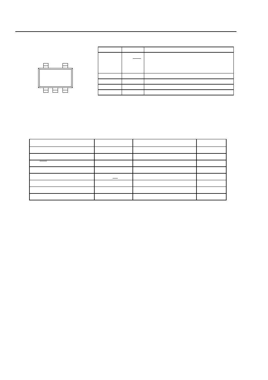
Block Diagram:
VSS
VOUT
L
SD
C
OUT
V
ON / OFF
ON / OFF
Reference Voltage
Source with Soft Start
+
-
PWM or
PWM/PFM-
Switched Control
Circuit
Note: The diode inside the IC is a parasitic diode.
Oscillation
Circuit
VIN
Tr
EXT
V
IN
C
IN
Figure 1 Block Diagram
Selection Guide:
1. Product Name
S - 852 X X XX MC - XXX - T2
Tape specifications.
Product name abbreviation.
Package name abbreviation.
Output voltage x 10
Product type:
A: Oscillation frequency of 180 kHz, with overload protection circuit.
B: Oscillation frequency of 180 kHz, without overload protection circuit.
C: Oscillation frequency of 60 kHz, with overload protection circuit.
D: Oscillation frequency of 60 kHz, without overload protection circuit.
E: Oscillation frequency of 300 kHz, with overload protection circuit.
F: Oscillation frequency of 300 kHz, without overload protection circuit.
Control system
0: PWM control
1: PWM/PFM-switched control
PWM Control & PWM/PFM Control Step-Down Switching Regulator-Controllers
Rev.7.4
_10
S-8520/8521 Series
Seiko Instruments Inc.
3
2. Product List (As of September 1, 2000)
A & B Series (Oscillation Frequency of 180 kHz)
Item
Output Voltage
(V)
S-8520AXXMC
Series
S-8521AXXMC
Series
S-8520BXXMC
Series
S-8521BXXMC
Series
1.6
1.8
S-8520B18MC-ARD-T2 S-8521B18MC-ATD-T2
1.9
S-8521B19MC-ATE-T2
2.0
S-8521B20MC-ATF-T2
2.1
S-8520A21MC-AVG-T2
S-8521B21MC-ATG-T2
2.5
S-8520A25MC-AVK-T2
S-8521A25MC-AXK-T2
S-8520B25MC-ARK-T2 S-8521B25MC-ATK-T2
2.7
S-8520A27MC-AVM-T2
S-8521A27MC-AXM-T2
S-8520B27MC-ARM-T2 S-8521B27MC-ATM-T2
2.8
S-8520A28MC-AVN-T2
S-8521A28MC-AXN-T2
S-8520B28MC-ARN-T2 S-8521B28MC-ATN-T2
2.9
S-8520A29MC-AVO-T2
S-8521A29MC-AXO-T2
S-8520B29MC-ARO-T2 S-8521B29MC-ATO-T2
3.0
S-8520A30MC-AVP-T2
S-8521A30MC-AXP-T2
S-8520B30MC-ARP-T2 S-8521B30MC-ATP-T2
3.1
S-8520A31MC-AVQ-T2
S-8521A31MC-AXQ-T2
S-8520B31MC-ARQ-T2 S-8521B31MC-ATQ-T2
3.2
S-8520A32MC-AVR-T2
S-8521A32MC-AXR-T2
S-8520B32MC-ARR-T2 S-8521B32MC-ATR-T2
3.3
S-8520A33MC-AVS-T2
S-8521A33MC-AXS-T2
S-8520B33MC-ARS-T2 S-8521B33MC-ATS-T2
3.4
S-8520A34MC-AVT-T2
S-8521A34MC-AXT-T2
S-8520B34MC-ART-T2
S-8521B34MC-ATT-T2
3.5
S-8520A35MC-AVU-T2
S-8521A35MC-AXU-T2
S-8520B35MC-ARU-T2 S-8521B35MC-ATU-T2
3.6
S-8520A36MC-AVV-T2
S-8521A36MC-AXV-T2
S-8520B36MC-ARV-T2 S-8521B36MC-ATV-T2
5.0
S-8520A50MC-AWJ-T2
S-8521A50MC-AYJ-T2
S-8520B50MC-ASJ-T2
S-8521B50MC-AUJ-T2
C & D Series (Oscillation Frequency of 60 kHz)
Item
Output Voltage
(V)
S-8520CXXMC
Series
S-8521CXXMC
Series
S-8520DXXMC
Series
S-8521DXXMC
Series
1.6
S-8521C16MC-BTB-T2
S-8521D16MC-BXB-T2
2.0
S-8521D20MC-BXF-T2
2.5
S-8520C25MC-BRK-T2 S-8521C25MC-BTK-T2
S-8520D25MC-BVK-T2 S-8521D25MC-BXK-T2
2.7
S-8520C27MC-BRM-T2 S-8521C27MC-BTM-T2
S-8520D27MC-BVM-T2 S-8521D27MC-BXM-T2
2.8
S-8520C28MC-BRN-T2 S-8521C28MC-BTN-T2
S-8520D28MC-BVN-T2 S-8521D28MC-BXN-T2
2.9
S-8520C29MC-BRO-T2 S-8521C29MC-BTO-T2
S-8520D29MC-BVO-T2 S-8521D29MC-BXO-T2
3.0
S-8520C30MC-BRP-T2 S-8521C30MC-BTP-T2
S-8520D30MC-BVP-T2 S-8521D30MC-BXP-T2
3.1
S-8520C31MC-BRQ-T2 S-8521C31MC-BTQ-T2
S-8520D31MC-BVQ-T2 S-8521D31MC-BXQ-T2
3.2
S-8520C32MC-BRR-T2 S-8521C32MC-BTR-T2
S-8520D32MC-BVR-T2 S-8521D32MC-BXR-T2
3.3
S-8520C33MC-BRS-T2 S-8521C33MC-BTS-T2
S-8520D33MC-BVS-T2 S-8521D33MC-BXS-T2
3.4
S-8520C34MC-BRT-T2
S-8521C34MC-BTT-T2
S-8520D34MC-BVT-T2
S-8521D34MC-BXT-T2
3.5
S-8520C35MC-BRU-T2 S-8521C35MC-BTU-T2
S-8520D35MC-BVU-T2 S-8521D35MC-BXU-T2
3.6
S-8520C36MC-BRV-T2 S-8521C36MC-BTV-T2
S-8520D36MC-BVV-T2 S-8521D36MC-BXV-T2
5.0
S-8520C50MC-BSJ-T2
S-8521C50MC-BUJ-T2
S-8520D50MC-BWJ-T2 S-8521D50MC-BYJ-T2
E & F Series (Oscillation Frequency of 300 kHz)
Item
Output Voltage
(V)
S-8520EXXMC
Series
S-8521EXXMC
Series
S-8520FXXMC
Series
S-8521FXXMC
Series
1.5
S-8521E15MC-BLA-T2
1.8
S-8520E18MC-BJD-T2 S-8521E18MC-BLD-T2
S-8520F18MC-BND-T2 S-8521F18MC-BPD-T2
2.0
S-8521E20MC-BLF-T2
2.5
S-8520E25MC-BJK-T2
S-8520F25MC-BNK-T2
2.7
S-8520F27MC-BNM-T2
3.0
S-8520E30MC-BJP-T2 S-8521E30MC-BLP-T2
S-8520F30MC-BNP-T2 S-8521F30MC-BPP-T2
3.3
S-8520E33MC-BJS-T2 S-8521E33MC-BLS-T2
S-8520F33MC-BNS-T2 S-8521F33MC-BPS-T2
3.4
S-8520F34MC-BNT-T2
3.5
S-8521E35MC-BLU-T2
5.0
S-8520E50MC-BKJ-T2 S-8521E50MC-BMJ-T2
S-8520F50MC-BOJ-T2
S-8521F50MC-BQJ-T2
For the availability of product samples listed above, contact the SII Sales Department.
PWM Control & PWM/PFM Control Step-Down Switching Regulator-Controllers
S-8520/8521 Series
Rev.7.4
_10
Seiko Instruments Inc.
4
Pin Assignment:
SOT-23-5
Top view
1 2 3
5 4
Figure 2
Absolute Maximum Ratings:
(Ta
= 25
C unless otherwise specified)
Item
Symbol
Ratings
Unit
VIN pin voltage
V
IN
*1
V
SS
-0.3 to V
SS
+12 or V
SS
+18
V
VOUT pin voltage
V
OUT
V
SS
-0.3 to V
SS
+12 or V
SS
+18
V
ON/OFF pin voltage
V
ON/OFF
*1
V
SS
-0.3 to V
SS
+12 or V
SS
+18
V
EXT pin voltage
V
EXT
V
SS
-0.3 to V
IN
+0.3
V
EXT pin current
I
EXT
±50
mA
Power dissipation
P
D
250
mW
Operating temperature range
T
OPR
-40 to +85
C
Storage temperature range
T
STG
-40 to +125
C
*1. V
SS
+12 V for S-8520/21A/C/E; V
SS
+18 V for S-8520/21B/D/F
Caution The absolute maximum ratings are rated values exceeding which the product
could suffer physical damage. These values must therefore not be exceeded under
any conditions.
Pin No.
Pin Name
Function
1
ON/OFF
Power-off pin
H: Normal operation (Step-down operation)
L: Step-down operation stopped (All circuits
deactivated)
2
VSS
GND pin
3
VOUT
Output voltage monitoring pin
4
EXT
Connection pin for external transistor
5
VIN
IC power supply pin

PWM Control & PWM/PFM Control Step-Down Switching Regulator-Controllers
Rev.7.4
_10
S-8520/8521 Series
Seiko Instruments Inc.
5
Electrical Characteristics:
1. S-8520/21 A & B Series
(Ta
=25 ∞C, unless otherwise specified)
Parameter
Symbol
Conditions
Min.
Typ.
Max.
Units
Measurement
Circuit
Output voltage
*1
V
OUT
(E)
-
V
OUT
(S)
◊ 0.976
V
OUT
(S)
V
OUT
(S)
◊1.024
V
3
Input voltage
V
IN
S-8520/21A Series
2.5
-
10.0
V
2
S-8520/21B Series
2.5
-
16.0
Current consumption 1
I
SS1
V
OUT
= V
OUT
(S)
◊ 1.2
-
35
60
µA
2
Current consumption during
power off
I
SSS
V
ON/OFF
= 0 V
-
-
0.5
µA
2
S-8520/21X15
- 24
-2.3
-4.5
-
S-8520/21X25
- 34
-3.7
-7.0
-
I
EXTH
V
EXT
=V
IN
-0.4 V
S-8520/21X35
- 44
-5.3
-9.3
-
S-8520/21X45
- 54
-6.7
-11.3
-
EXT pin output current
S-8520/21X55
- 60
-8.0
-13.3
-
mA
-
S-8520/21X15
- 24
+4.3
+8.4
-
S-8520/21X25
- 34
+7.0
+13.2
-
I
EXTL
V
EXT
= 0.4 V
S-8520/21X35
- 44
+9.9
+17.5
-
S-8520/21X45
- 54
+12.6
+21.4
-
S-8520/21X55
- 60
+15.0
+25.1
-
Line regulation
V
OUT1
V
IN
= V
OUT
(S)
◊1.2 to ◊1.4
*4
-
30
60
mV
3
Load regulation
V
OUT2
Load current
=10µA to I
OUT
(See below)
◊1.25
-
30
60
mV
3
Output voltage temperature
coefficient
V
OUT
/
Ta
Ta
= - 40
∞C to 85
∞C
-
±V
OUT
(S)
◊ 5E-5
-
V/
∞C
3
Oscillation frequency
fosc
Measure waveform
at EXT pin
V
OUT
(S)
2.5 V
153
180
207
kHz
3
V
OUT
(S)
2.4 V
144
180
216
PWM/PFM-control switch
duty ratio
*2
PFM Duty Measure waveform at EXT pin under no
load.
15
25
40
%
3
Power-Off pin
V
SH
Evaluate oscillation at EXT pin
1.8
-
-
V
2
input voltage
V
SL
Evaluate oscillation stop at EXT pin
-
-
0.3
Power-Off pin
I
SH
-
-0.1
-
0.1
µA
1
input leakage current
I
SL
-
-0.1
-
0.1
µA
1
Soft-Start time
T
SS
-
4.0
8.0
16.0
ms
3
Overload detection time
*3
T
PRO
Duration from the time V
OUT
is reduced
to 0 V to the time the EXT pin obtains
V
IN
.
2.0
4.0
8.0
ms
2
Efficiency
EFFI
-
-
93
-
%
3
Conditions:
The recommended components are connected to the IC, unless otherwise indicated. V
IN
= V
OUT
(S)
◊ 1.2 [V],
I
OUT
= 120 [mA] (V
IN
= 2.5 V, if V
OUT
(S)
2.0 V.)
Peripheral components:
Coil
: Sumida Electric Co., Ltd. CD54 (47
µH).
Diode
: Matsushita Electronics Corporation MA720 (Schottky type).
Capacitor
: Matsushita Electronics Corporation TE (16 V, 22
µF tantalum type).
Transistor
: Toshiba Corporation 2SA1213Y.
Base resistance (R
b
)
: 0.68 k
Base capacitor (C
b
)
: 2200 pF (Ceramic type)
The power-off pin is connected to VIN.
Notes:
The output voltage indicated above represents a typical output voltage set up. These specifications apply in
common to both S-8520 and S-8521, unless otherwise noted.
*1. V
OUT
(S) Specified output voltage value.
V
OUT
(E) Actual output voltage value.
*2. Applicable to the S-8521A Series and S-8521B Series.
*3. Applicable to the S-8520A Series and S-8521A Series.
*4. V
IN
= 2.5 V to 2.94 V, if V
OUT
(S)
2.0 V.