Document Outline
- S-8533 Series
- Cover
- Features
- Applications
- Package
- Block Diagram
- Selection Guide
- Pin Assignment
- Absolute Maximum Ratings
- Electrical Characteristics
- Measurement Circuits
- Operation
- Selection of External Components
- Standard Circuits
- Precautions
- Characteristics of Major Parameters (Typical values)
- Transient Response Characteristics
- Reference Data
- Package Drawing

Rev.1.2
_00
SYNCHRONOUS PWM CONTROL
STEP-DOWN SWITCHING REGULATOR-CONTROLLERS
S-8533 Series
Seiko Instruments Inc.
1
The S-8533 series is a synchronous PWM control
CMOS step-down switching regulator controller that
includes a reference voltage source, synchronous
circuit, an oscillation circuit, an error amplifier, a
phase compensation circuit, and a PWM controller.
An efficient step-down switching regulator can be
realized simply by adding external Pch and Nch
power MOSFETs, one coil, and three capacitors.
Since the oscillation frequency is a high 300 kHz, the
S-8533 can be used to configure a high efficiency
step-down switching regulator capable of driving high
output current using small external components and
a 3 to 10% in-crease in efficiency is obtained
compared to conventional step-down switching
regulators.
The 8-Pin TSSOP and high oscillation frequency
make the S-8533 ideal as the main power supply for
portable devices.
Features
∑ Synchronous rectification system realizing high efficiency (typ. 94%)
∑ Use at maximum duty = 100% and use of a battery up to maximum life is possible by using Pch and Nch
MOS transistors externally.
∑ Oscillation frequency:
300 kHz
∑ Input voltage:
2.7 to 16.0 V
∑ Output voltage:
1.25 V
1.3 to 6.0 V, selectable in 0.1 V steps
∑ Output voltage accuracy:
Ī2.0%
∑ Soft start
Can be set by an external capacitance CSS.
∑ Power-off function
∑ Small package
8-Pin TSSOP
Applications
∑ Constant voltage power supply for hard disks and DVD drivers
∑ Power supplies for portable devices, such as digital cameras, PDAs, electronic organizers, and cellular
phones
∑ Main or sub power supply for notebook computers and peripheral equipment
∑ Constant voltage power supply for cameras, video equipment, and communication devices
Package
∑ 8-Pin TSSOP (Package drawing code: FT008-A)
SYNCHRONOUS PWM CONTROL STEP-DOWN SWITCHING REGULATOR-CONTROLLERS
S-8533 Series
Rev.1.2
_00
Seiko Instruments Inc.
2
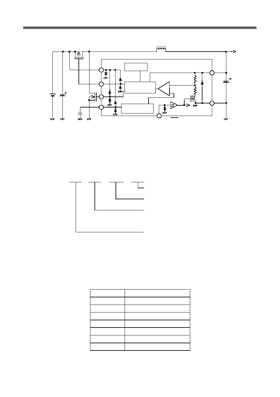
Block Diagram
VSS
VOUT
L
C
OUT
Remark The diode inside the IC is a parasitic diode.
Reference voltage
source with soft start
PWM control circuit
P.N feed-through
prevention circuit
Oscillation
circuit
VIN
Tr
Tr
C
SS
CSS
PDRV
NDRV
V
IN
C
IN
+
-
ON / OFF
Figure 1 Block diagram
Selection Guide
1. Product name selection guide
S-8533A xx X FT ≠ TB
IC direction in tape specifications
*1
Package name (abbreviation)
FT: 8-Pin TSSOP
*2
Output voltage2
*2
A : 1.3 to 6.0 V
5 : 1.25V
Output voltage1
*2
13 to 55
(E.g., when the output voltage is 1.5 V, it is
expressed as 15.)
The product whose output voltage is 1.25 V
expresses 12.
*1. Refer to the taping specifications at the end of this book.
2. Product Name List
Output voltage
Product Name
1.25 V
S-8533A125FT-TB
1.5 V
S-8533A15AFT-TB
1.8 V
S-8533A18AFT-TB
2.5 V
S-8533A25AFT-TB
2.7 V
S-8533A27AFT-TB
3.3 V
S-8533A33AFT-TB
5.0 V
S-8533A50AFT-TB
SYNCHRONOUS PWM CONTROL STEP-DOWN SWITCHING REGULATOR-CONTROLLERS
Rev.1.2
_00
S-8533 Series
Seiko Instruments Inc.
3
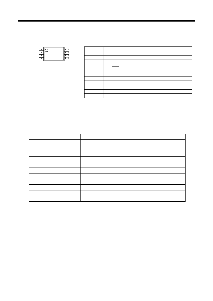
Pin Assignment
3
4
2
1
6
5
7
8-pin TSSOP
Top View
8
Figure 2
*1. NC indicates no electrical connection.
Therefore, even connecting to VIN or VSS does not cause a
problem.
Absolute Maximum Ratings
(Ta
= 25įC unless otherwise specified)
Parameter Symbol Ratings Unit
VIN pin voltage
V
IN
V
SS
- 0.3 to V
SS
+ 18
V
VOUT pin voltage
V
OUT
V
SS
- 0.3 to V
SS
+ 18
V
ON/OFF pin voltage
V
ON/OFF
V
SS
- 0.3 to V
SS
+ 18
V
CSS pin voltage
V
CSS
V
SS
- 0.3 to V
IN
+ 0.3
V
NDRV pin voltage
V
NDRV
V
SS
- 0.3 to V
IN
+ 0.3
V
PDRV pin voltage
V
PDRV
V
SS
- 0.3 to V
IN
+ 0.3
V
NDRV pin current
I
NDRV
PDRV pin current
I
PDRV
Ī100 mA
Power dissipation
P
D
300
mW
Operating temperature range
T
opr
-40 to +85
įC
Storage temperature range
T
stg
-40 to +125
įC
Caution The absolute maximum ratings are rated values exceeding which the product could
suffer physical damage. These values must therefore not be exceeded under any
conditions.
Pin No. Pin Name
Function
1 NC
No connection
*1
2
VOUT Output voltage pin
3
ON/ OFF
Power-off pin
H: Normal operation (Step-down operation)
L: Halts step-down operation (All circuits
deactivated)
4
CSS
Soft start capacitor connection pin
5 VSS
GND
pin
6
NDRV External N channel connection pin
7
PDRV External P channel connection pin
8
VIN
IC power supply pin

SYNCHRONOUS PWM CONTROL STEP-DOWN SWITCHING REGULATOR-CONTROLLERS
S-8533 Series
Rev.1.2
_00
Seiko Instruments Inc.
4
Electrical Characteristics
V
IN
= V
OUT
◊ 1.5 [V], I
OUT
= V
OUT
/ 50 [A] (In case V
OUT
1.8 [V], V
IN
= 2.7 [V] ) (Ta = 25 įC, unless otherwise specified)
Parameter Symbol
Conditions
Min.
Typ.
Max.
Units
Measure-
ment
Circuit
Output voltage
*1
V
OUT(E)
V
OUT(S)
◊ 0.98
V
OUT(S)
V
OUT(S)
◊ 1.02
V 2
Input voltage
V
IN
2.7
-
16.0 V
1
Current consumption 1
I
SS1
No external components, V
OUT
= V
OUT(S)
◊ 0.95
(Duty ratio 100%)
-
30 70
ĶA
1
Current consumption
during power-off
I
SSS
ON/
OFF pin
= 0 V
-
-
1.0
ĶA
1
I
PDRVH
No external components, V
OUT
= V
OUT(S)
◊ 1.5,
V
IN
= 9.0 V, V
PDRV
= V
IN
- 0.2 V
-12
-18
-
mA 1
PDRV pin output current
I
PDRVL
No external components, V
OUT
= V
OUT(S)
◊ 0.95
V
IN
= 9.0 V, V
PDRV
= 0.2 V
19 27
-
mA 1
I
NDRVH
No external components, V
OUT
= V
OUT(S)
◊ 1.5,
V
IN
= 9.0 V, V
NDRV
= V
IN
- 0.2 V
-10
-14
-
mA 1
NDRV pin output current
I
NDRVL
No external components, V
OUT
= V
OUT(S)
◊ 0.95
V
IN
= 9.0 V, V
NDRV
= 0.2 V
35 50
-
mA 1
V
IN
= V
OUT(S)
◊ 1.2
S-8533A125,
S-8533A13A to 29A
-
V
OUT(E)
◊ 1.0 %
V
OUT(E)
◊ 2.5 %
V 2
Line regulation
V
OUT1
to 16 V
*2
S-8533A30A to 60A
-
V
OUT(E)
◊ 1.0 %
V
OUT(E)
◊ 2.0 %
V 2
Load regulation
V
OUT2
I
OUT
= 10
ĶA to I
OUT
(see above)
◊ 1.25
-
V
OUT(E)
◊ 0.5 %
V
OUT(E)
◊ 1.0 %
V 2
Output voltage
temperature coefficient
V
Ta V
OUT
OUT
∑
Ta
= 40įC to 85įC
-
Ī100
-
ppm/
įC
-
Oscillation frequency
fosc
Measure waveform at the PDRV pin.
255
300
345
kHz
2
Maximum duty ratio
MaxDuty See l
SS1
. Measure waveform at the PDRV pin.
100
-
-
% 1
VOUT pin input current
I
VOUT
V
OUT
= 5.0 V.
0.01 0.1 4.0
ĶA
1
ON/
OFF pin
V
SH
See I
SS1
.
V
IN
= 2.7 V and check that PDRV pin = "L".
1.8
-
-
V 1
input voltage
V
SL
See I
SS1
.
V
IN
= 16.0 V and check that PDRV pin = "H".
-
-
0.3 V 1
ON/
OFF pin
I
SH
See I
SS1
. ON/
OFF pin
= V
IN
.
-0.1
-
0.1
ĶA
1
Input leakage current
I
SL
See I
SS1
. ON/
OFF pin
= 0 V.
-0.1
-
0.1
ĶA
1
Soft-Start time
t
SS
See
I
SS1
. Measure time until PDRV pin oscillates.
5.0
8.0
16.0
ms
1
Efficiency EFFI
*3, I
OUT
= 200mA to 400mA, S-8533A33A
-
94
-
% 3
External components:
Coil:
Sumida Corporation
CD105 (22
ĶH)
Diode:
Matsushita Electric Industrial Co., Ltd. MA737 (Schottky diode)
Capacitor:
Nichicon Corporation
F93 (16 V, 47
ĶF, tantalum) ◊ 2
Transistor:
Toshiba
Corporation
2SA1213-Y
Base
resistor: 1
k
Base
capacitor: 2200
pF
C
SS
: 4700
pF
C
NDRV
: 1000
pF
*1. V
OUT(S)
: Nominal output voltage value
V
OUT(E)
: Actual output voltage value: V
IN
= V
OUT
◊ 1.5[V], I
OUT
= V
OUT
/50[A] (If V
OUT
1.8[V], V
IN
= 2.7[V].)
*2. In case V
OUT(S)
2.2 [V], V
IN
= 2.7 to 16 [V]
*3. External components
Coil:
Sumida Corporation
CDRH104R (22
ĶH)
Capacitor:
Nichicon Corporation
F93 (16 V, 47
ĶF, tantalum) ◊ 2
Pch POWER MOS:
Sanyo Electric Co., Ltd. CPH6303 (V
GS
10 V max.)
Nch POWER MOS:
Sanyo Electric Co., Ltd. CPH6403 (V
GS
10 V max.)
C
SS
: 4700
pF
SYNCHRONOUS PWM CONTROL STEP-DOWN SWITCHING REGULATOR-CONTROLLERS
Rev.1.2
_00
S-8533 Series
Seiko Instruments Inc.
5
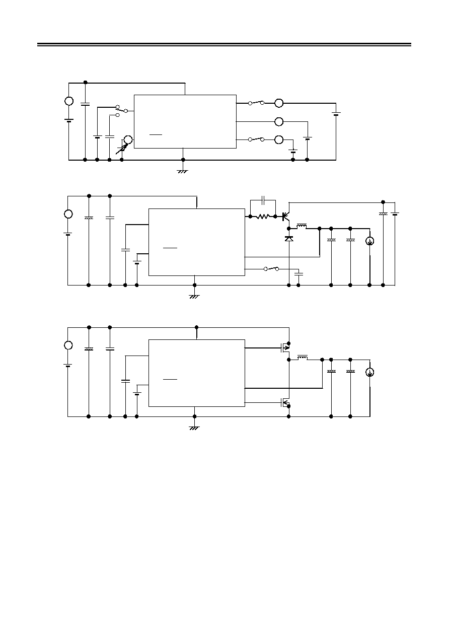
Measurement Circuits
VSS
0.1
ĶF
ON/OFF
1
CSS
PDRV
VOUT
NDRV
VIN
A
A
A
A
A
4700 pF
22
ĶF◊3
4700 pF
VSS
0.1
ĶF
CNDRV
1000 pF
CD105
22
ĶH
MA737
2SA1213
2200 pF
1 k
F93
47
ĶF
F93
47
ĶF
F93
22
ĶF◊3
F93
+
+
+
+
ON/OFF
2
CSS
PDRV
VOUT
NDRV
VIN
A
4700 pF
22
ĶF
CDRH104R
VSS
0.1
ĶF
22
ĶH
I
OUT
CPH6403
CPH6303
F93
47
ĶF
F93
47
ĶF
F93
+
+
+
ON/OFF
3
CSS
PDRV
VOUT
NDRV
VIN
A
Figure 3
SYNCHRONOUS PWM CONTROL STEP-DOWN SWITCHING REGULATOR-CONTROLLERS
S-8533 Series
Rev.1.2
_00
Seiko Instruments Inc.
6
Operation
1. Synchronous PWM control step-down DC/DC converter
1.1 Synchronous rectification
A synchronous rectifying DC/DC converter enables a greater reduction in the power consumption of the
external rectifying element compared with a conventional DC/DC converter. In addition, incorporating a
P and N feed-through prevention circuit reduces the feed-through current during operation of external
transistors (Pch and Nch), making the operating power consumption extremely low.
1.2 PWM Control
The S-8533 series uses pulse width modulation (PWM) and is characterized by its low current
consumption.
In pulse frequency modulation (PFM) DC/DC converters, pulses are skipped when they operate at low
output current, causing variations in the ripple frequency of the output voltage and increase in the ripple
voltage both of which constitute inherent drawbacks to these converters.
In the S-8533 series, the pulse width varies in the range from 0% to 100% according to the load current,
yet the ripple voltage produced by the switching can easily be removed by a filter since the switching
frequency is always constant. These converters thus provide low-ripple output voltage over wide range
of input voltage and load current.
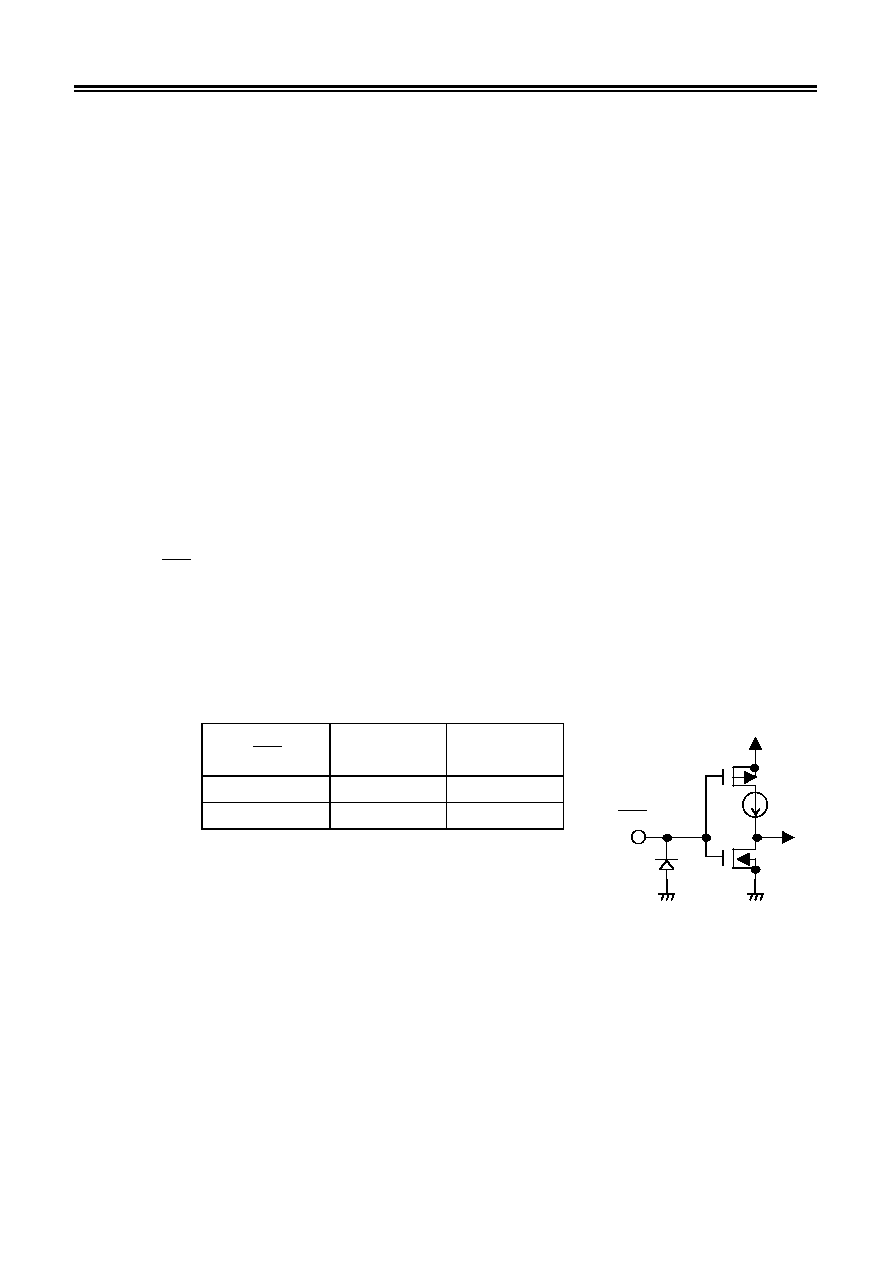
2. Power-off Function
This function activates and deactivates the step-down operation and is controlled by the power-off pin
(ON/ OFF pin). When the power-off pin is set "L", the voltage of the PDRV pin goes to V
IN
level and
voltage of the NDRV pin goes to V
SS
level to shut off both the MOSFETs. All the internal circuits stop
working, and substantial saving in current consumption is thus achieved.
The power-off pin has configuration shown in Figure 4. Since pull-up or pull-down is not performed
internally, operation where the power-off pin is in a floating state should be avoided. Application of a
voltage of 0.3 V to 1.8 V to the pin should also be avoided lest the current consumption increases.
When the power-off pin is not used, it should be connected to the VIN pin.
ON/ OFF pin
CR Oscillation
Circuit
Output Voltage
"H" Active
Set
value
"L" Non-active
OPEN
Figure 4
ON/OFF
V
IN
V
SS
SYNCHRONOUS PWM CONTROL STEP-DOWN SWITCHING REGULATOR-CONTROLLERS
Rev.1.2
_00
S-8533 Series
Seiko Instruments Inc.
7
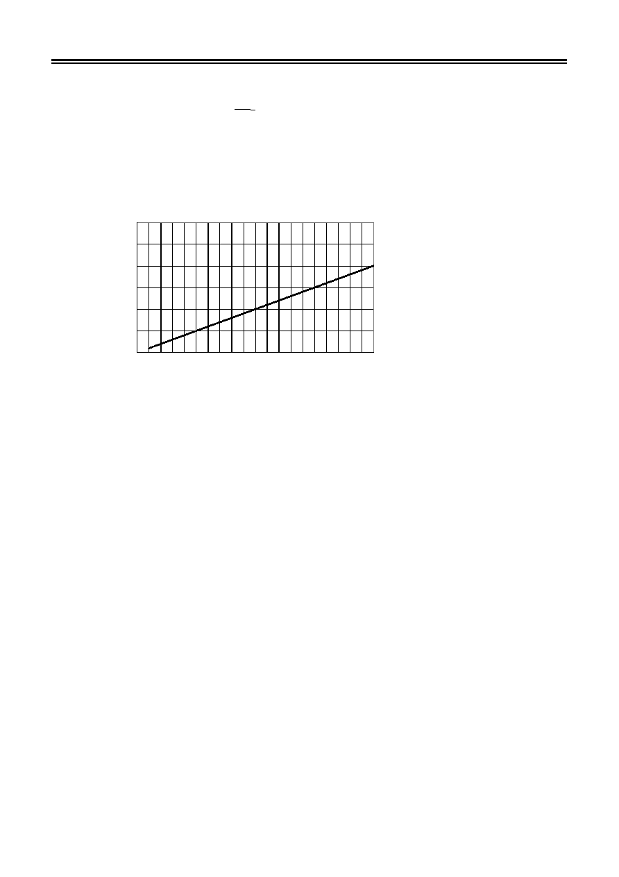
3. Soft-Start
Function
The S-8533 series has a built-in soft-start circuit. This circuit enables the output voltage to ramp
gradually over the specified soft-start time to suppress the overshooting of the output voltage, when the
power is switched on or the ON/OFF pin is set "H".
The soft-start time can be set with an external capacitance (C
SS
). The capacitance value of the C
SS
should be selected so as to make enough soft-start time for the power rising time. If the C
SS
value is not
enough, output voltage overshooting, input current rushing or IC malfunction may occur. The time
needed for output voltage (V
OUT
) to reach 95% of the set value is calculated by the following formula.
Soft-start time
0
10
20
30
40
50
60
0
5000
10000
15000
20000
External capacitance C
SS
(pF)
Soft-start time (ms)
Figure 5 Soft-start time vs. external capacitance
4. 100% Duty Cycle
The S-8533 series operates up to the maximum duty cycle of 100%. The switching transistor is kept on
continuously to supply current to the load, when the input voltage falls below the preset output voltage
value. The output voltage in this case is equal to the subtraction of the lowering due to the DC
resistance of the coil and the on resistance of the switching FET from the input voltage.
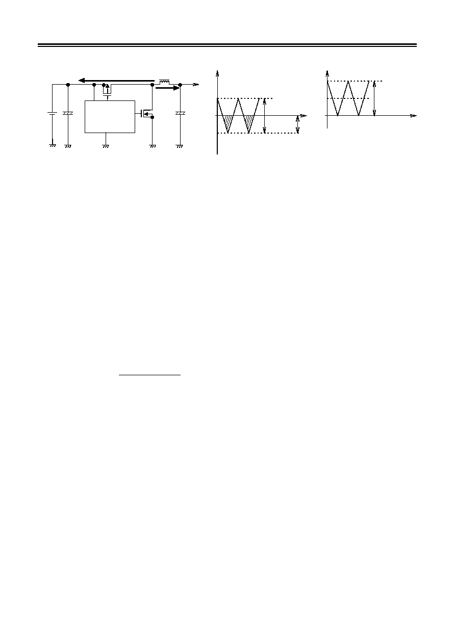
5. Back-flow
current
Since the S-8533 series performs PWM synchronous rectification under a light load, current flows back
to the V
IN
direction. And the back-flow current is the biggest when there is no load (see Fig. 6.). Since
the maximum back-flow current value is calculated by the following equation, attention should be paid to.
Duty(I
OUT
= 0) = V
OUT
/V
IN
Example: V
IN
= 5 V, V
OUT
= 3 V, Duty = 60%
IL = V/L ◊ ton = (V
IN
- V
OUT
)
◊ Duty/(L ◊ fosc) ◊ 1.2
Example: V
IN
= 5 V, V
OUT
= 3 V, fosc = 300 kHz, L = 22 ĶH, IL = 218 mA
Ilmax
= IL/2 = 109 mA, Ilmin = -IL/2 = -109 mA
When there is no load, the coil current becomes triangular wave with I
L
max the maximum and I
L
min the
minimum which is negative. The negative current, hatched parts in Fig. 7, flows backward.
When the output current (I
OUT
) is approximately 109 mA under the above conditions, the current does
not flow backward since the minimum value (I
L
min) of the triangular wave becomes 0 mA. When an
input capacitor (C
IN
) is installed, back-flow current to the power source is negligible since the back-flow
current is absorbed by the input capacitor. The input capacitor is indispensable to reduce back-flow
current to the power source.
Though the fore mentioned conditions are required to prevent back-flow current, they are guidelines.
Please check the validity by measuring the prototype or the actual device.
Formula for calculating soft-start time (t
SS
)
t
SS
(ms)
= 0.002 ◊ C
SS
(pF)
SYNCHRONOUS PWM CONTROL STEP-DOWN SWITCHING REGULATOR-CONTROLLERS
S-8533 Series
Rev.1.2
_00
Seiko Instruments Inc.
8
Back-flow current
C
IN
+
V
IN
Coil
current I
L
L
PDRV
NDRV
Coil current under no load
Coil current when 109 mA
flows as a load
Back-flow
current
-109 mA
109 mA
I
L
min
I
L
max
I
L
I
L
V
OUT
VIN
VSS
0 mA
Back-flow current
= 0 mA
0 mA
I
OUT
109 mA
I
OUT
218 mA
I
L
min
I
L
max
I
L
I
L
+
Figure 6 Back-flow current
Figure 7 Example for no back-flow current
Selection of External Components
1. Inductor
The inductance value L greatly affects the maximum output current I
OUT
and the efficiency
.
As the Inductance is reduced gradually, the peak current I
PK
increases, and the output current I
OUT
reaches the maximum at a certain Inductance value. As the Inductance is made even smaller, I
OUT
begins to decrease since the current drivability of the switching transistor becomes insufficient.
Conversely, as the Inductance is increased, the loss in the switching transistor due to I
PK
decreases, and
the efficiency reaches the maximum at a certain Inductance value. As the Inductance is made even
larger, the efficiency degrades since the loss due to the series resistance of the inductor increases.
In many applications an inductance of 22
ĶH will yield the best characteristics of the S-8533 series in a
well balanced manner.
When choosing an inductor, attention to its allowable current should be paid since the current applied
over the allowable value will cause magnetic saturation in the inductor, leading to a marked decline in
efficiency.
An inductor should therefore be selected so as not the peak current I
PK
to surpass its allowable current.
The peak current I
PK
is expressed by the following equation:
IN
OSC
OUT
IN
OUT
OUT
PK
V
L
f
2
)
V
(V
V
I
I
◊
◊
◊
-
◊
+
=
where f
OSC
(
= 300 kHz) is the oscillation frequency and L is the inductance value of the inductor.
2. Capacitors
(C
IN
, C
OUT
)
The capacitor (C
IN
) inserted on the input side serves to reduce power impedance, average input current
and suppress back-flow current to the power source. Choose the C
IN
value according to the impedance
of the power source used, and choose a capacitor with a large capacitance and a low ESR (Equivalent
Series Resistance). It should be 47 to 100
ĶF, although the actual value depends on the impedance of
the power source used and load current value. When the input voltage is low and the load is large, the
output voltage may become unstable. In this case increase the input capacitance.
For the output side capacitor (C
OUT
), select a large capacitance with low ESR (Equivalent Series
Resistance) to smoothen the ripple voltage. When the input voltage is extremely high or the load current
is extremely large, the output voltage may become unstable. In this case the unstable area will become
narrow by selecting a large capacitance for an output side capacitor. A tantalum electrolytic capacitor is
recommended since the unstable area widens when a capacitor with a large ESR, such as an aluminum
electrolytic capacitor, or a capacitor with a small ESR, such as a ceramic capacitor, is chosen. The
range of the capacitance should generally be 47
ĶF to 100 ĶF.
When selecting an input capacitor and an output capacitor, evaluate them by testing under the actual
conditions.

SYNCHRONOUS PWM CONTROL STEP-DOWN SWITCHING REGULATOR-CONTROLLERS
Rev.1.2
_00
S-8533 Series
Seiko Instruments Inc.
9
3. External Switching Transistor
Enhancement (Pch, Nch) MOSFETs are recommended as external switching transistors for the S-8533
series.
3.1 Enhancement MOSFET
The PDRV/NDRV pin of the S-8533 series is capable of directly driving a Pch or Nch power MOSFET
with a gate capacity around 1000 pF.
When a Pch/Nch power MOSFETs are chosen, efficiency will be 2 to 3% higher than that achieved by
bipolar transistor since MOSFET switching speeds are higher than PNP/NPN bipolar transistors and
power losses due to the base current are avoided.
The important parameters in selecting Pch/Nch power MOSFETs are the threshold voltage, breakdown
voltage between gate and source, breakdown voltage between drain and source, total gate capacity, on-
resistance, and the current ratings.
The PDRV/NDRV pin swings from voltage V
IN
over to voltage V
SS
. If the input voltage is low, a MOSFET
with a low threshold voltage has to be used so that the MOSFET will turn on as required. If, conversely,
the input voltage is high, select a MOSFET whose gate-source breakdown voltage is higher than the
input voltage by at least several volts.
Immediately after the power is turned on, or when the power is turned off (that is, when the step-down
operation is terminated), the input voltage will be applied across the drain and the source of the
MOSFET. The transistor therefore needs to have drain-source breakdown voltage that is also several
volts higher than the input voltage.
The total gate capacity and the on-resistance affect the efficiency.
The power loss for charging and discharging the gate capacity by switching operation will affect the
efficiency especially at low load current region when the total gate capacity becomes larger and the input
voltage becomes higher. If the efficiency at low load is a matter of concern, select a MOSFET with a
small total gate capacity.
In regions where the load current is high, the efficiency is affected by power losses caused by the on-
resistance of the MOSFET. If the efficiency under heavy load is particularly important in the application,
choose a MOSFET having on-resistance as low as possible.
As for the current rating, select a MOSFET whose maximum continuous drain current rating is higher
than the peak current I
PK
.
If an external Pch MOSFET has much different characteristics (input capacitance, Vth, etc.) from an
external Nch MOSFET, they turn ON at the same time, flowing a through current and reducing efficiency.
If a MOSFET with a large input capacitance is used, switching loss increases and efficiency decreases.
If it is used at several hundreds of mA or more, the loss at the MOSFET increases and may exceed the
permissible loss of the MOSFET. To select Pch and Nch MOSFETs, evaluate the performance by
testing under the actual condition. If the load current is large, the Pch MOSFET loss increases and heat
is generated. Pay attention to dissipate heat from the Pch MOSFET.
For reference, some efficiency data is included in this document. For applications with an input voltage
range of 6 to 8 V or less, data was obtained by using Sanyo Co., Ltd. CPH6303, CPH6403, and Vishay
Siliconix Si3441DV, Si3442DV, and for applications with an input voltage range of 6 to 8 V or more, data
was obtained by using Sanyo Co., Ltd. CPH6302, CHP6402, and Vishay Siliconix Si3454DV, Si3455DV.
See "Reference Data".
Current flow in the parasitic diode is not allowed in some MOSFETs. In this case, a schottky diode must
be connected in parallel to the MOSFET. The schottky diode must have a low forward voltage, a high
switching speed, a reverse-direction withstand voltage of V
IN
or higher, and a current rating of I
PK
or
higher.
SYNCHRONOUS PWM CONTROL STEP-DOWN SWITCHING REGULATOR-CONTROLLERS
S-8533 Series
Rev.1.2
_00
Seiko Instruments Inc.
10
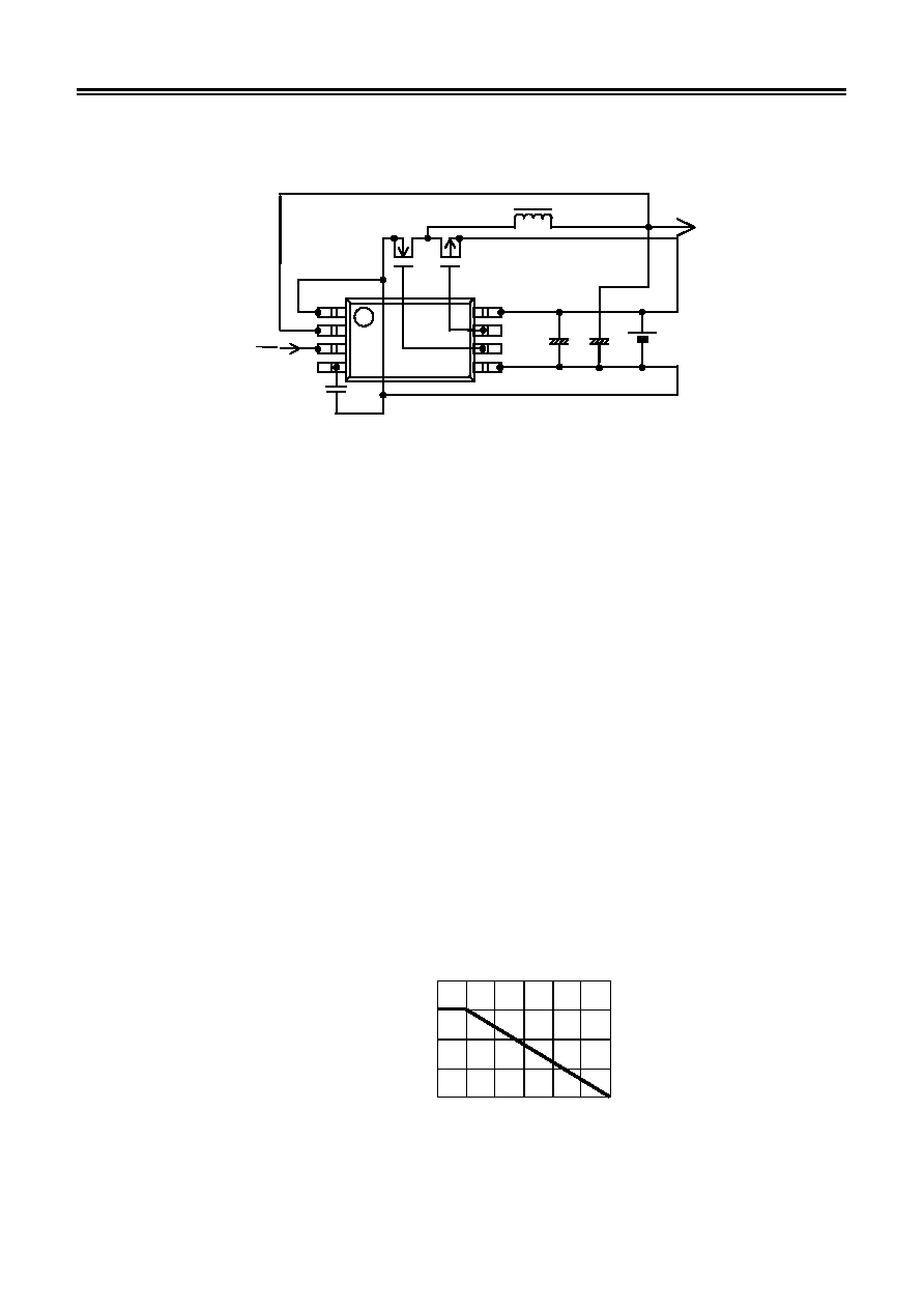
Standard Circuits
∑ Using MOSFET transistors
L
V
IN
Nch Power
MOS FET
C
OUT
C
IN
V
OUT
Pch Power
MOS FET
1
8
4 5
C
SS
S-8533
V
ON / OFF
+
+
Figure 8
Caution The above connection diagram does not guarantee correct operation. Perform
sufficient evaluation using the actual application to set the constants.
Precautions
Install the external capacitors, diode, coil, and other peripheral components as close to the IC as
possible, and make a one-point grounding.
Normally, the Pch and Nch MOSFETs do not turn ON at the same time. However, if the external Pch
MOSFET has much different characteristics (input capacitance, V
th
, etc.) from the external Nch
MOSFET, they may turn ON at the same time, flowing a through current. Select Pch and Nch transistors
with similar characteristics.
Any switching regulator intrinsically produces ripple voltage and spike noise, which are largely dictated by
the coil and capacitors in use. When designing a circuit, first test them under actual condition.
If the input voltage is high and output current is low, pulses with a low duty ratio may be output, and then
the duty ratio may be 0% for several clocks.
The PDRV and NDRV oscillation frequencies may be an integer fraction of 300 kHz at some input
voltage and load conditions. In this case, the ripple voltage may increase.
The through current prevention circuit reduces through current by shifting the Pch and Nch transistor on
timing. It does not suppress the through current in the external transistors completely.
Since PWM synchronous rectification is performed even when the load is light, current flows back to V
IN
.
Check whether the back-flow occurs and whether it affects the performance. (See 5. Back-flow current.)
The PDRV or NDRV oscillation frequency may vary in a voltage range, depending on input voltage.
When decreasing the power supply voltage slowly, the IC operation may be undefined if the voltage falls
below the minimum operating voltage.
Do not apply an electrostatic discharge to this IC that exceeds the performance ratings of the built-in
electrostatic protection circuit.
Make sure that dissipation of the switching transistor will not surpass the allowable power dissipation of
the package (especially at high temperature).
0
300
400
100
200
0
50
100
150
Power
dissipation
P
D
(mW)
Ambient temperature Ta (įC)
Figure 9 8-Pin TSSOP Package Power Dissipation in Free Air
Seiko Instruments Inc. shall bear no responsibility for any patent infringement by a product that includes
an IC manufactured by Seiko Instruments Inc. in relation to the method of using the IC in that product,
the product specifications, or the destination country.

SYNCHRONOUS PWM CONTROL STEP-DOWN SWITCHING REGULATOR-CONTROLLERS
Rev.1.2
_00
S-8533 Series
Seiko Instruments Inc.
11
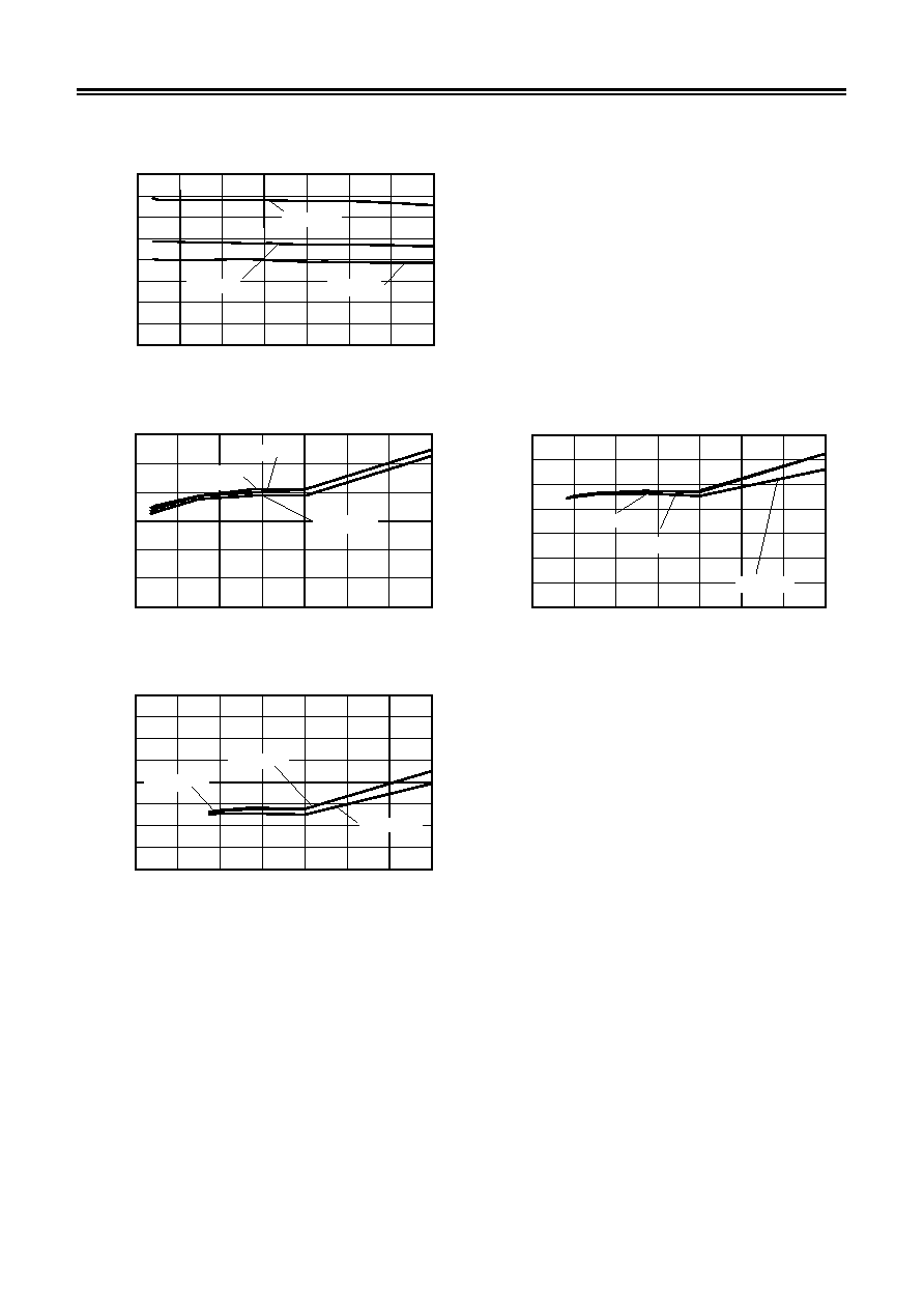
Characteristics of Major Parameters (Typical values)
0
1
2
3
4
5
6
7
8
9
10
2
4
6
8
1
1
1
1
6
Ta
= 25įC
Ta
= -40įC
Ta
= 85įC
I
SS1
(
ĶA)
V
IN
(V)
240
260
280
300
320
340
360
2
4
6
8
10
12
14
16
Ta
= 25įC
Ta
= -40įC
Ta
= 85įC
V
IN
(V)
fosc
(kHz)
0
10
20
30
40
50
60
70
2
4
6
8
10
12
14
16
Ta
= 85įC
Ta
= -40įC
Ta
= 25įC
V
IN
(V)
0
10
20
30
40
50
60
70
2
4
6
8
10
12
14
16
Ta
= -40įC
Ta
= 25įC
Ta
= 85įC
V
IN
(V)
0
10
20
30
40
50
60
70
2
4
6
8
10
12
14
16
Ta
= 85įC
Ta
= 25įC
Ta
= -40įC
V
IN
(V)
0
20
40
60
80
100
120
2
4
6
8
10
12
14
16
Ta
= -40įC
Ta
= 25įC
Ta
= 85įC
V
IN
(V)
0.0
0.2
0.4
0.6
0.8
1.0
1.2
1.4
1.6
1.8
2
4
6
8
10
12
14
16
Ta
= 85įC
Ta
= 25įC
Ta
= -40įC
V
IN
(V)
0.3
0.5
0.7
0.9
1.1
1.3
1.5
1.7
2
4
6
8
10
12
14
16
Ta
= -40įC
Ta
= 25įC
Ta
= 85įC
V
IN
(V)
(1) I
SS1
vs. V
IN
(2) fosc vs. V
IN
(3) I
PDRVH
vs. V
IN
(4) I
PDRVL
vs. V
IN
(5) I
NDRVH
vs. V
IN
(6) I
NDRVL
vs. V
IN
(7) V
SH
vs. V
IN
(8) V
SL
vs. V
IN
I
PDRVH
(mA)
I
PDRVL
(mA)
I
NDRVH
(mA)
I
NDRVL
(mA)
V
SH
(V)
V
SL
(V)
SYNCHRONOUS PWM CONTROL STEP-DOWN SWITCHING REGULATOR-CONTROLLERS
S-8533 Series
Rev.1.2
_00
Seiko Instruments Inc.
12
0
2
4
6
8
10
12
14
16
2
4
6
8
10
12
14
16
Ta
= 85įC
Ta
= 25įC
Ta
= -40įC
V
IN
(V)
(9) t
SS
vs. V
IN
(10) V
OUT
vs. V
IN
(1.5 V: S-8533A15AFT)
(11) V
OUT
vs. V
IN
(3.3 V: S-8533A33AFT)
(12) V
OUT
vs. V
IN
(5.0 V: S-8533A50AFT)
t
SS
(mS)
1.47
1.48
1.49
1.50
1.51
1.52
1.53
2
4
6
8
10
12
14
16
I
OUT
= 100 mA
I
OUT
= 0.1 mA
I
OUT
= 400 mA
V
IN
(V)
4.92
4.94
4.96
4.98
5.00
5.02
5.04
5.06
5.08
2
4
6
8
10
12
14
16
I
OUT
= 100 mA
I
OUT
= 0.1 mA
I
OUT
= 400 mA
V
IN
(V)
3.23
3.25
3.27
3.29
3.31
3.33
3.35
3.37
2
4
6
8
10
12
14
16
I
OUT
= 0.1 mA
I
OUT
= 100 mA
I
OUT
= 400 mA
SYNCHRONOUS PWM CONTROL STEP-DOWN SWITCHING REGULATOR-CONTROLLERS
Rev.1.2
_00
S-8533 Series
Seiko Instruments Inc.
13
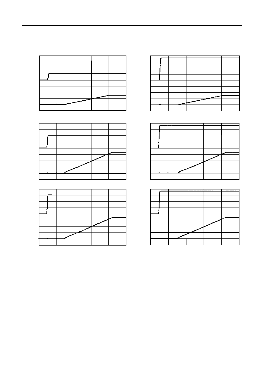
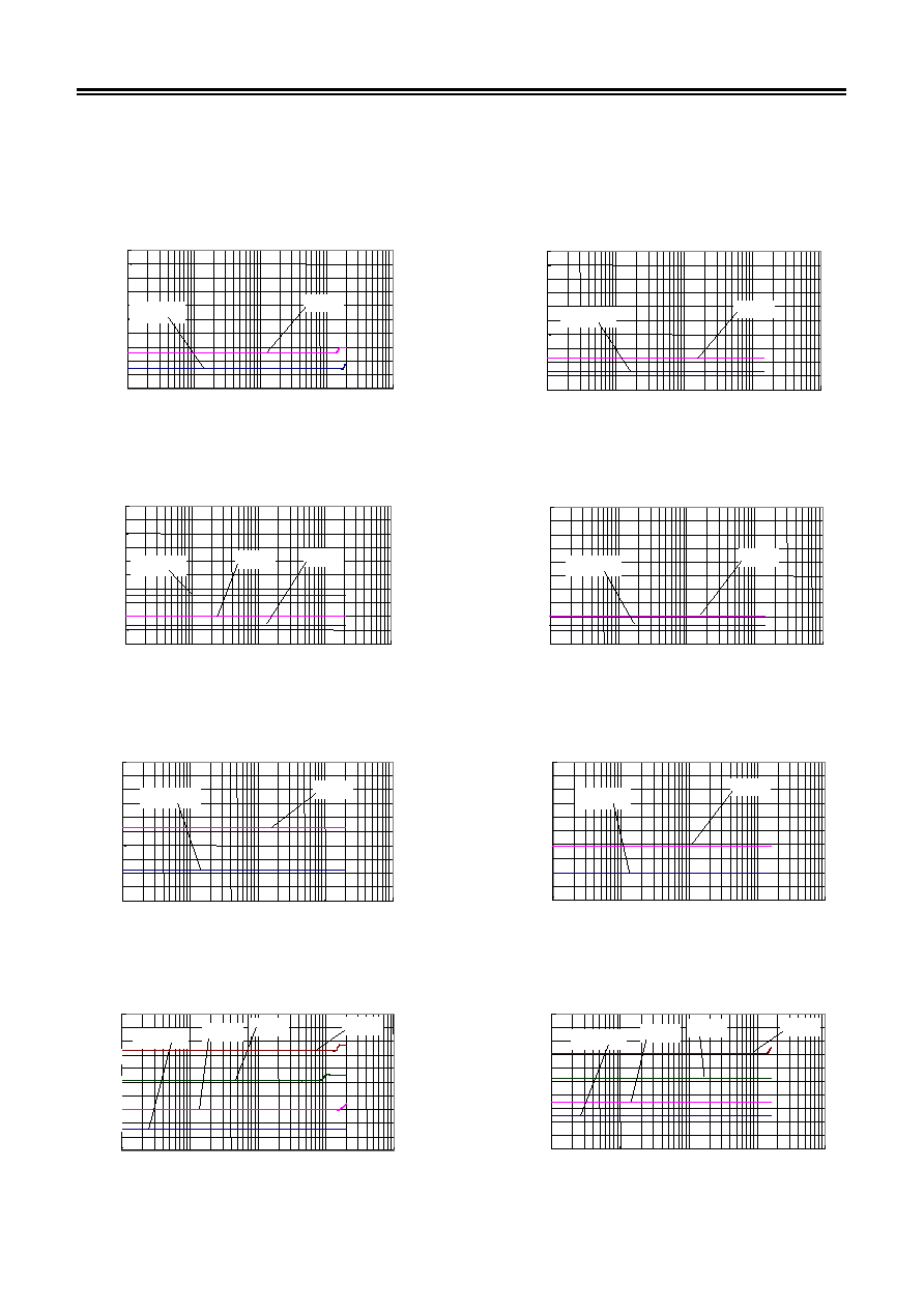
Transient Response Characteristics
1. Power Application (Vin: 0 V
2.7 V or 5.0 V or 7.5 V, 0 V 9.0 V I
OUT
: 10 mA)
t (2 ms/div)
Input voltage
(2.5 V/div)
3 V
0 V
Output voltage
(1 V/div)
0 V
t (2 ms/div)
10 V
Input voltage
(2.5 V/div)
0 V
3 V
Output voltage
(1 V/div)
0 V
t (2 ms/div)
Input voltage
(2.5 V/div)
0 V
3 V
0 V
t (2 ms/div)
10 V
Input voltage
(2.5 V/div)
4.5 V
0 V
Output voltage
(1.5 V/div)
0 V
t (2 ms/div)
10 V
0 V
4.5 V
0 V
t (2 ms/div)
0 V
3 V
0 V
10 V
10 V
Input voltage
(2.5 V/div)
Output voltage
(1 V/div)
10 V
Output voltage
(1 V/div)
Input voltage
(2.5 V/div)
Output voltage
(1.5 V/div)
(1) S-8533A15AFT (V
IN
: 0
2.7 V)
(2) S-8533A15AFT (V
IN
: 0
9.0 V)
(4) S-8533A33AFT (V
IN
: 0
9.0 V)
(3) S-8533A33AFT (V
IN
: 0
5.0 V)
(5) S-8533A50AFT (V
IN
: 0
7.5 V)
(6) S-8533A50AFT (V
IN
: 0
9.0 V)
SYNCHRONOUS PWM CONTROL STEP-DOWN SWITCHING REGULATOR-CONTROLLERS
S-8533 Series
Rev.1.2
_00
Seiko Instruments Inc.
14
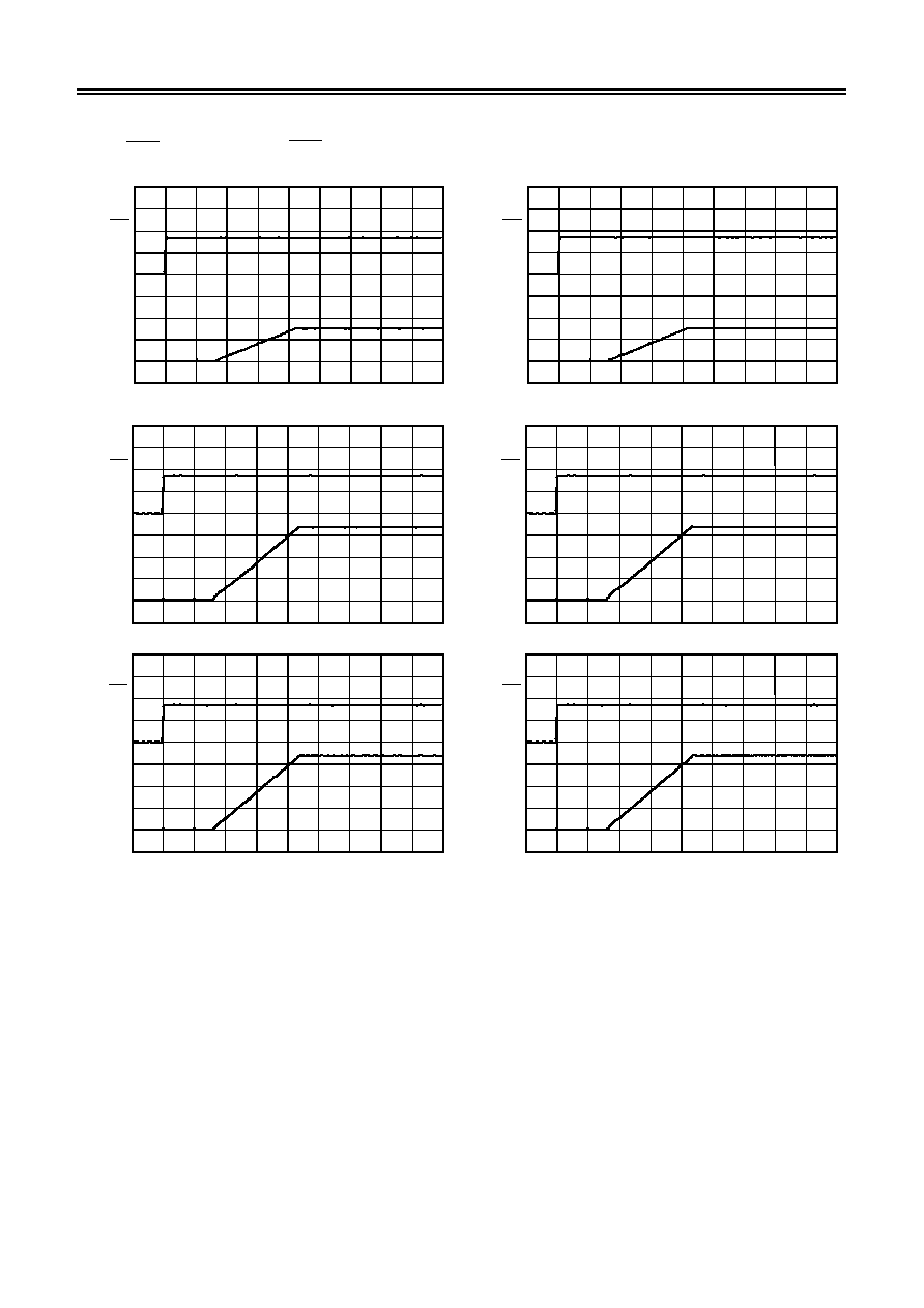
2. ON/OFF Pin response (ON/OFF: 0 V
1.8 V I
OUT
: 10 mA)
t (2 ms/div)
ON/OFF
Pin voltage
(1 V/div)
4 V
0 V
3 V
Output voltage
(1 V/div)
0 V
t (2 ms/div)
4 V
ON/OFF
Pin voltage
(1 V/div)
0 V
3 V
Output voltage
(1 V/div)
0 V
t (2 ms/div)
4 V
ON/OFF
Pin voltage
(1 V/div)
0 V
3 V
Output voltage
(1 V/div)
0 V
t (2 ms/div)
4 V
0 V
3 V
Output voltage
(1 V/div)
0 V
t (2 ms/div)
4 V
ON/OFF
Pin voltage
(1 V/div)
0 V
4.5 V
Output voltage
(1.5 V/div)
0 V
t (2 ms/div)
4 V
ON/OFF
Pin voltage
(1 V/div)
0 V
4.5 V
Output voltage
(1.5 V/div)
0 V
ON/OFF
Pin voltage
(1 V/div)
(1) S-8533A15AFT (V
IN
: 2.7 V)
(2) S-8533A15AFT (V
IN
: 9.0 V)
(3) S-8533A33AFT (V
IN
: 5.0 V)
(4) S-8533A33AFT (V
IN
: 9.0 V)
(5) S-8533A50AFT (V
IN
: 7.5 V)
(6) S-8533A50AFT (V
IN
: 9.0 V)
SYNCHRONOUS PWM CONTROL STEP-DOWN SWITCHING REGULATOR-CONTROLLERS
Rev.1.2
_00
S-8533 Series
Seiko Instruments Inc.
15
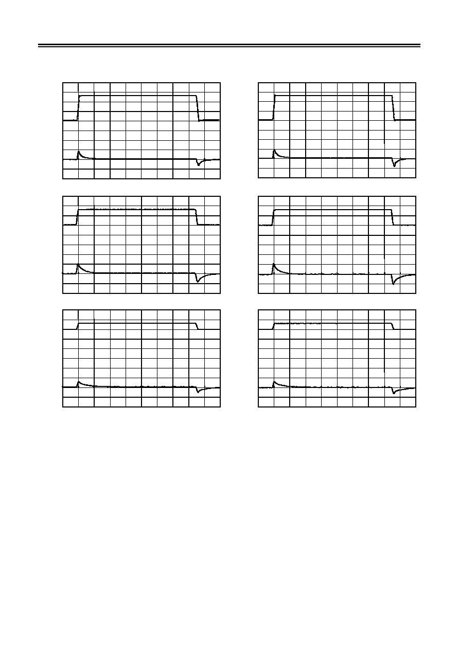
3. Power Supply Voltage Variation (Vin: 2.7 V
9.0 V 2.7 V, 5.0 V 9.0 V 5.0 V, 7.5 V 9.0 V 7.5 V)
t (0.5 ms/div)
0 V
10 V
t (0.5 ms/div)
10 V
0 V
t (0.5 ms/div)
10 V
0 V
t (0.5 ms/div)
10 V
0 V
t (0.5 ms/div)
10 V
0 V
t (0.5 ms/div)
10 V
0 V
Output voltage
(0.1 V/div)
Input voltage
(2.5 V/div)
Input voltage
(2.5 V/div)
Output voltage
(0.1 V/div)
Output voltage
(0.1 V/div)
Input voltage
(2.5 V/div)
Input voltage
(2.5 V/div)
Output voltage
(0.1 V/div)
Output voltage
(0.1 V/div)
Input voltage
(2.5 V/div)
Input voltage
(2.5 V/div)
Output voltage
(0.1 V/div)
(1) S-8533A15AFT (I
OUT
: 10 mA)
(2) S-8533A15AFT (I
OUT
: 500 mA)
(3) S-8533A33AFT (I
OUT
: 10 mA)
(4) S-8533A33AFT (I
OUT
: 500 mA)
(5) S-8533A50AFT (I
OUT
: 10 mA)
(6) S-8533A50AFT (I
OUT
: 500 mA)
SYNCHRONOUS PWM CONTROL STEP-DOWN SWITCHING REGULATOR-CONTROLLERS
S-8533 Series
Rev.1.2
_00
Seiko Instruments Inc.
16
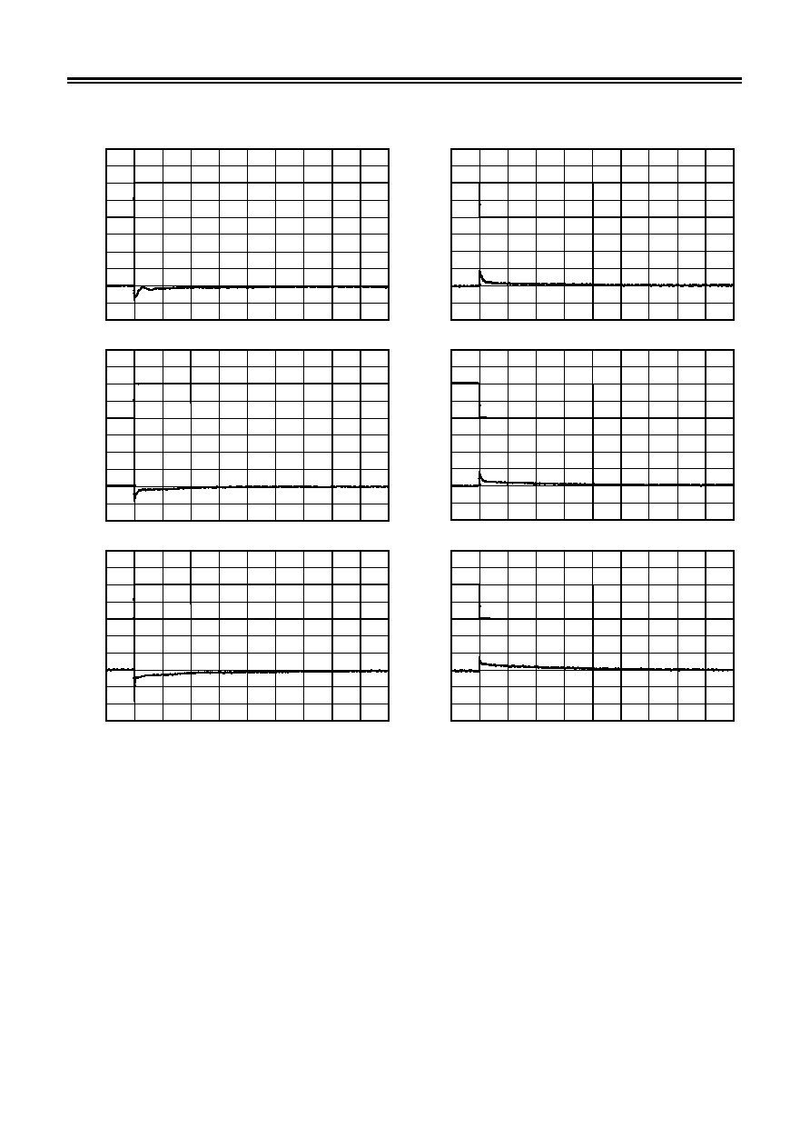
4. Load Variation (Vin: 2.7 V or 5.0 V or 7.5 V I
OUT
: 0.1 mA
500 mA, 500 mA 0.1 mA)
t (0.1 ms/div)
0.1 mA
t (0.1 ms/div)
0.1 mA
t (0.1 ms/div)
0.1 mA
t (0.1 ms/div)
0.1 mA
t (0.1 ms/div)
t (0.1 ms/div)
0.1 mA
Output
voltage
(0.1 V/div)
Output
current
500 mA
Output
voltage
(0.1 V/div)
Output
current
500 mA
Output
voltage
(0.1 V/div)
Output
current
500 mA
500 mA
Output
current
Output
voltage
(0.1 V/div)
Output
current
Output
voltage
(0.1 V/div)
500 mA
Output
voltage
(0.1 V/div)
Output
current
500 mA
0.1 mA
(1) S-8533A15AFT (V
IN
: 2.7 V)
(2) S-8533A15AFT (V
IN
: 2.7 V)
(3) S-8533A33AFT (V
IN
: 5.0 V)
(4) S-8533A33AFT (V
IN
: 5.0 V)
(5) S-8533A50AFT (V
IN
: 7.5 V)
(6) S-8533A50AFT (V
IN
: 7.5 V)
SYNCHRONOUS PWM CONTROL STEP-DOWN SWITCHING REGULATOR-CONTROLLERS
Rev.1.2
_00
S-8533 Series
Seiko Instruments Inc.
17
Reference Data
Reference data are intended for use in selecting peripheral components to the IC. The information therefore
provides characteristic data in which external components are selected with a view of wide variety of IC
applications. All data show typical values.
External components list for efficiency vs output current characteristics
Table 1
No. Product Name V
OUT
Pch
MOSFET
Nch
MOSFET
Inductor C
OUT
C
IN
Application Condition
(1) S-8533A15AFT 1.5
V CPH6303 CPH6403 CDRH104R/22
ĶH 47 ĶF ◊ 2 47
ĶF, 0.1 ĶF I
OUT
2 A, V
IN
8 V
(2) S-8533A15AFT 1.5 V
Si3441
Si3442
CDRH104R /22
ĶH 47 ĶF ◊ 2 47
ĶF, 0.1 ĶF I
OUT
1.4 A, V
IN
6 V
(3) S-8533A33AFT 3.3 V
CPH6303
CPH6403 CDRH104R /22
ĶH 47 ĶF ◊ 2 47
ĶF, 0.1 ĶF I
OUT
2 A, V
IN
8 V
(4) S-8533A33AFT 3.3 V
Si3441
Si3442
CDRH104R /22
ĶH 47 ĶF ◊ 2 47
ĶF, 0.1 ĶF I
OUT
1.4 A, V
IN
6 V
(5) S-8533A33AFT 3.3 V
CPH6302
CPH6402 CDRH104R /22
ĶH 47 ĶF ◊ 2 47
ĶF, 0.1 ĶF I
OUT
2 A, V
IN
16 V
(6) S-8533A33AFT 3.3 V
Si3455
Si3454
CDRH104R /22
ĶH 47 ĶF ◊ 2 47
ĶF, 0.1 ĶF I
OUT
1.6 A, V
IN
16 V
(7) S-8533A50AFT 5.0 V
CPH6302
CPH6402 CDRH104R /22
ĶH 47 ĶF ◊ 2 47
ĶF, 0.1 ĶF I
OUT
2 A, V
IN
16 V
(8) S-8533A50AFT 5.0 V
Si3455
Si3454
CDRH104R /22
ĶH 47 ĶF ◊ 2 47
ĶF, 0.1 ĶF I
OUT
1.6 A, V
IN
16 V
(9) S-8533A15AFT 1.5 V
CPH6303
CPH6403 CDRH104R /47
ĶH 47 ĶF ◊ 2 47
ĶF, 0.1 ĶF I
OUT
2 A, V
IN
8 V
(10) S-8533A15AFT 1.5 V
Si3441
Si3442
CDRH104R /47
ĶH 47 ĶF ◊ 2 47
ĶF, 0.1 ĶF I
OUT
1.4 A, V
IN
6 V
(11) S-8533A33AFT 3.3 V
CPH6303
CPH6403 CDRH104R /47
ĶH 47 ĶF ◊ 2 47
ĶF, 0.1 ĶF I
OUT
2 A, V
IN
8 V
(12) S-8533A33AFT 3.3 V
Si3441
Si3442
CDRH104R /47
ĶH 47 ĶF ◊ 2 47
ĶF, 0.1 ĶF I
OUT
1.4 A, V
IN
6 V
(13) S-8533A33AFT 3.3 V
CPH6302
CPH6402 CDRH104R /47
ĶH 47 ĶF ◊ 2 47
ĶF, 0.1 ĶF I
OUT
2 A, V
IN
16 V
(14) S-8533A33AFT 3.3 V
Si3455
Si3454
CDRH104R /47
ĶH 47 ĶF ◊ 2 47
ĶF, 0.1 ĶF I
OUT
1.6 A, V
IN
16 V
(15) S-8533A50AFT 5.0 V
CPH6302
CPH6402 CDRH104R /47
ĶH 47 ĶF ◊ 2 47
ĶF, 0.1 ĶF I
OUT
2 A, V
IN
16 V
(16) S-8533A50AFT 5.0 V
Si3455
Si3454
CDRH104R /47
ĶH 47 ĶF ◊ 2 47
ĶF, 0.1 ĶF I
OUT
1.6 A, V
IN
16 V
(17) S-8533A15AFT 1.5 V
CPH6303
CPH6403 CDRH104R /10
ĶH 47 ĶF ◊ 2 47
ĶF, 0.1 ĶF I
OUT
2 A, V
IN
8 V
(18) S-8533A15AFT 1.5 V
Si3441
Si3442
CDRH104R /10
ĶH 47 ĶF ◊ 2 47
ĶF, 0.1 ĶF I
OUT
1.4 A, V
IN
6 V
(19) S-8533A33AFT 3.3 V
CPH6303
CPH6403 CDRH104R /10
ĶH 47 ĶF ◊ 2 47
ĶF, 0.1 ĶF I
OUT
2 A, V
IN
8 V
(20) S-8533A33AFT 3.3 V
Si3441
Si3442
CDRH104R /10
ĶH 47 ĶF ◊ 2 47
ĶF, 0.1 ĶF I
OUT
1.4 A, V
IN
6 V
(21) S-8533A33AFT 3.3 V
CPH6302
CPH6402 CDRH104R /10
ĶH 47 ĶF ◊ 2 47
ĶF, 0.1 ĶF I
OUT
2 A, V
IN
16 V
(22) S-8533A33AFT 3.3 V
Si3455
Si3454
CDRH104R /10
ĶH 47 ĶF ◊ 2 47
ĶF, 0.1 ĶF I
OUT
1.6 A, V
IN
16 V
(23) S-8533A50AFT 5.0 V
CPH6302
CPH6402 CDRH104R /10
ĶH 47 ĶF ◊ 2 47
ĶF, 0.1 ĶF I
OUT
2 A, V
IN
16 V
(24) S-8533A50AFT 5.0 V
Si3455
Si3454
CDRH104R /10
ĶH 47 ĶF ◊ 2 47
ĶF, 0.1 ĶF I
OUT
1.6 A, V
IN
16 V
(25) S-8533A33AFT 3.3
V CPH6303 CPH6403 CDRH125
/10
ĶH 47
ĶF ◊ 2 47
ĶF, 0.1 ĶF I
OUT
3 A, V
IN
8 V
(26) S-8533A33AFT 3.3
V CPH6302 CPH6402 CDRH125
/10
ĶH 47
ĶF ◊ 2 47
ĶF, 0.1 ĶF I
OUT
3 A, V
IN
16 V
SYNCHRONOUS PWM CONTROL STEP-DOWN SWITCHING REGULATOR-CONTROLLERS
S-8533 Series
Rev.1.2
_00
Seiko Instruments Inc.
18
External components list for ripple voltage vs output current characteristics
Table 2
No. Product
Name V
OUT
Pch
MOSFET
Nch
MOSFET
Inductor C
OUT
C
IN
Application
Condition
(27) S-8533A15AFT 1.5
V CPH6303 CPH6403 CDRH104R/22
ĶH 47
ĶF ◊ 2 47 ĶF, 0.1 ĶF I
OUT
2 A, V
IN
8 V
(28) S-8533A15AFT 1.5 V
Si3441
Si3442
CDRH104R /22
ĶH 47
ĶF ◊ 2 47 ĶF, 0.1 ĶF I
OUT
1.4 A, V
IN
6 V
(29) S-8533A33AFT 3.3
V CPH6303 CPH6403 CDRH104R
/22
ĶH 47
ĶF ◊ 2 47 ĶF, 0.1 ĶF I
OUT
2 A, V
IN
8 V
(30) S-8533A33AFT 3.3 V
Si3441
Si3442
CDRH104R /22
ĶH 47
ĶF ◊ 2 47 ĶF, 0.1 ĶF I
OUT
1.4 A, V
IN
6 V
(31) S-8533A33AFT 3.3
V CPH6302 CPH6402 CDRH104R
/22
ĶH 47
ĶF ◊ 2 47 ĶF, 0.1 ĶF I
OUT
2 A, V
IN
16 V
(32) S-8533A33AFT 3.3 V
Si3455
Si3454
CDRH104R /22
ĶH 47
ĶF ◊ 2 47 ĶF, 0.1 ĶF I
OUT
1.6 A, V
IN
16 V
(33) S-8533A50AFT 5.0
V CPH6302 CPH6402 CDRH104R
/22
ĶH 47
ĶF ◊ 2 47 ĶF, 0.1 ĶF I
OUT
2 A, V
IN
16 V
(34) S-8533A50AFT 5.0 V
Si3455
Si3454
CDRH104R /22
ĶH 47
ĶF ◊ 2 47 ĶF, 0.1 ĶF I
OUT
1.6 A, V
IN
16 V
Performance Data
Table 3
Parts
Product
Name
Manufacturer
Inductance
(
ĶH)
DC
Resistance(
)
Maximum
Current (A)
Diameter
(mm)
Height
(mm)
CDRH125
Sumida
Corporation
10 0.019
4.0
12.0 typ.
12.3.max.
8.0 max.
47 0.095
1.9
22 0.054
2.5
Inductor
CDRH104R
Sumida
Corporation
10 0.026
3.8
10.2 typ.
10.5.max.
4.0 max.
Diode MA737
Matsushita
Electric Industrial
Co., Ltd
Forward current 1.5 A (@VF
= 0.5 V)
Output Capacity
F93
Nichicon
Corporation
CPH6303
Sanyo
Electric Co., Ltd
V
GS
10 V max. , I
D
-4 A max., Vth -0.4 V min., C
ISS
820 pF typ.
Ron 0.090
max. (V
GS
= -4 V), CPH6
CPH6302
Sanyo
Electric Co., Ltd
V
GS
20 V max. , I
D
≠3 A max., Vth
-1.0 V min., C
ISS
300 pF typ.
Ron 0.145
max. (V
GS
= -10 V), CPH6
Si3441DV
Vishay
Silliconix
V
GS
8 V max. , I
D
-3.3 A max., Vth -0.45 V min.,
Ron 0.10
max. (V
GS
= -4.5 V),TSOP-6
External Transistor
(Pch MOSFET)
Si3455DV
Vishay
Silliconix
V
GS
20 V max. , I
D
-3.5 A max., Vth -1.0 V min.,
Ron 0.10
max. (V
GS
= -10 V), TSOP-6
CPH6403
Sanyo Co., Ltd
Electric
V
GS
10 V max. , I
D
6 A max. , Vth 0.4 V min., C
ISS
700 pF typ.
Ron 0.038
max. (V
GS
= 4 V), CPH6
CPH6402
Sanyo Co., Ltd
Electric
V
GS
24 V max. , I
D
4 A max. , Vth 1.0 V min., C
ISS
240 pF typ.
Ron 0.075
max. (V
GS
= 10 V), CPH6
Si3442DV
Vishay
Silliconix
V
GS
8 V max. , I
D
4.0 A max. , Vth 0.6 V min.,
Ron 0.070
max. (V
GS
= 4.5 V), TSOP-6
External Transistor
(Nch MOSFET)
Si3454DV
Vishay
Silliconix
V
GS
20 V max. , I
D
4.2 A max. , Vth 1.0 V min.,
Ron 0.065
max. (V
GS
= 10 V), TSOP-6
SYNCHRONOUS PWM CONTROL STEP-DOWN SWITCHING REGULATOR-CONTROLLERS
Rev.1.2
_00
S-8533 Series
Seiko Instruments Inc.
19
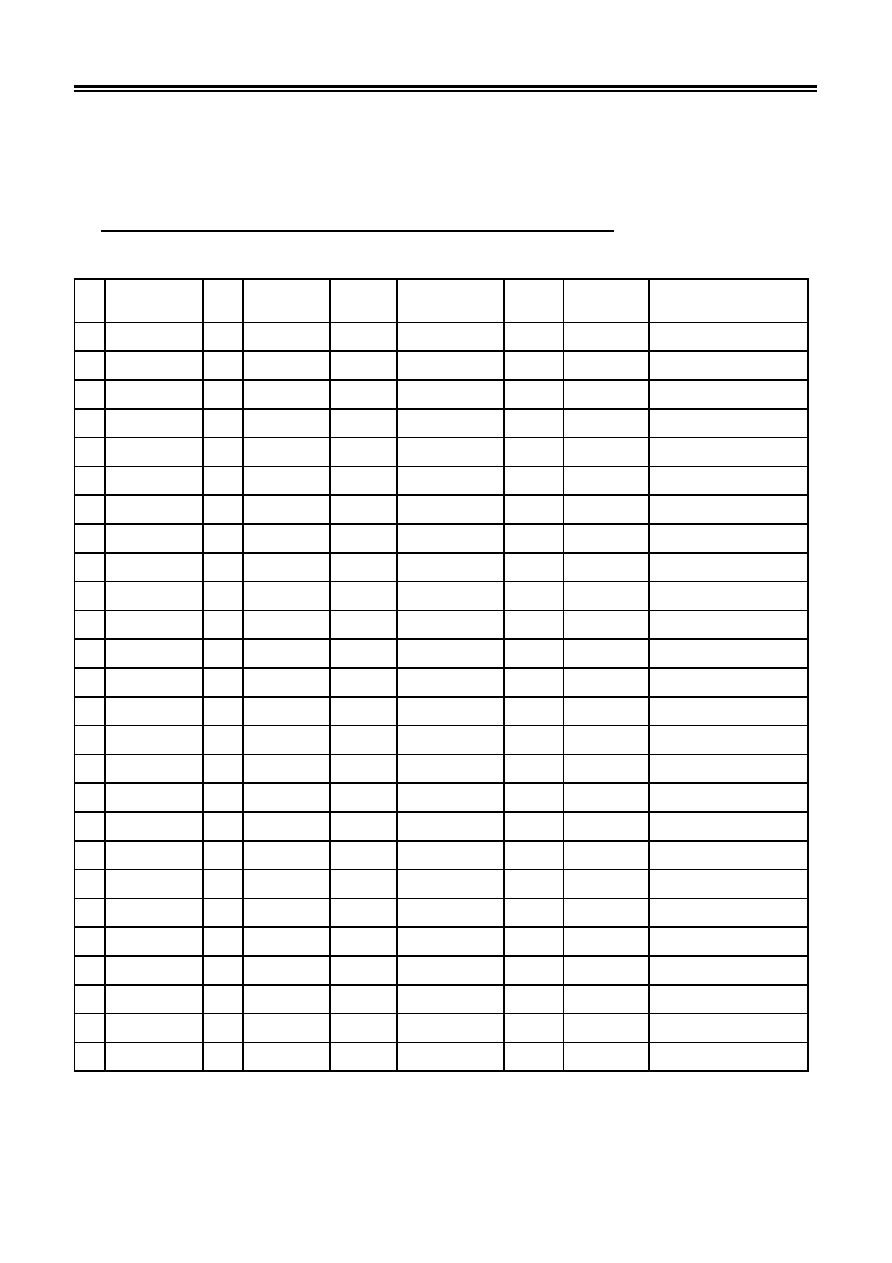
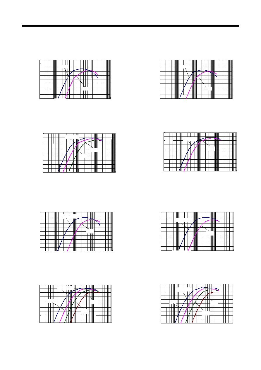
1. Efficiency Characteristics
50
55
60
65
70
75
80
85
90
95
100
1
10
100
1000
10000
Output current (mA)
E
f
fi
c
i
ency
(%
)
50
55
60
65
70
75
80
85
90
95
100
1
10
100
1000
10000
Output current (mA)
V
IN
= 2.7 V
5.0 V
V
IN
= 2.7 V
5.0 V
E
f
fi
c
i
ency
(%
)
50
55
60
65
70
75
80
85
90
95
100
1
100
1000
10000
Output current (mA)
50
55
60
65
70
75
80
85
90
95
100
1
100
1000
10000
Output current (mA)
10
10
V
IN
= 4.0 V
4.95 V
7.0 V
V
IN
= 4.0 V
4.95 V
E
f
fi
c
i
ency
(%
)
E
f
fi
c
i
ency
(%
)
50
55
60
65
70
75
80
85
90
95
100
1
100
1000
10000
(mA)
50
55
60
65
70
75
80
85
90
95
100
1
100
1000
10000
(mA)
10
Output current
10
Output current
V
IN
= 4.95 V
10 V
V
IN
= 4.95 V
10 V
E
f
fi
c
i
ency
(%
)
E
f
fi
c
i
ency
(%
)
50
55
60
65
70
75
80
85
90
95
100
1
100
1000
10000
(mA)
50
55
60
65
70
75
80
85
90
95
100
1
100
1000
10000
(mA)
10
Output current
10
Output current
V
IN
= 6.0 V
16 V
10 V
7.5 V
V
IN
= 6.0 V
16 V
10 V
7.5 V
E
f
fi
c
i
ency
(%
)
E
f
fi
c
i
ency
(%
)
(1) S-8533A15AFT
Efficiency vs. Output current (CPH6303/CPH6403)
(2) S-8533A15AFT
Efficiency vs. Output current (Si3441DV/Si3442DV)
(3) S-8533A33AFT
Efficiency vs. Output current (CPH6303/CPH6403)
(4) S-8533A33AFT
Efficiency vs. Output current (Si3441DV/Si3442DV)
(5) S-8533A33AFT
Efficiency vs. Output current (CPH6302/CPH6402)
(6) S-8533A33AFT
Efficiency vs. Output current (Si3454DV/Si3455DV)
(7) S-8533A50AFT
Efficiency vs. Output current (CPH6302/CPH6402)
(8) S-8533A50AFT
Efficiency vs. Output current (Si3454DV/Si3455DV)
SYNCHRONOUS PWM CONTROL STEP-DOWN SWITCHING REGULATOR-CONTROLLERS
S-8533 Series
Rev.1.2
_00
Seiko Instruments Inc.
20
50
55
60
65
70
75
80
85
90
95
100
1
10
100
1000
10000
Output current (mA)
V
IN
= 2.7 V
5.0 V
50
55
60
65
70
75
80
85
90
95
100
1
10
100
1000
10000
Output current (mA)
V
IN
= 2.7 V
5.0 V
E
f
fi
c
i
ency
(%
)
E
f
fi
c
i
ency
(%
)
50
55
60
65
70
75
80
85
90
95
100
1
100
1000
10000
(mA)
50
55
60
65
70
75
80
85
90
95
100
100
1000
10000
Output current (mA)
Output current
10
10
1
V
IN
= 4.0 V
4.95 V
7.0 V
V
IN
= 4.0 V
4.95 V
E
f
fi
c
i
ency
(%
)
E
f
fi
c
i
ency
(%
)
50
55
60
65
70
75
80
85
90
95
100
1
100
1000
10000
(mA)
50
55
60
65
70
75
80
85
90
95
100
1
10
100
1000
10000
Output current (mA)
10
Output current
V
IN
= 4.95 V
10 V
10 V
V
IN
= 4.95 V
E
f
fi
c
i
ency
(%
)
E
f
fi
c
i
ency
(%
)
50
55
60
65
70
75
80
85
90
95
100
1
100
1000
10000
(mA)
50
55
60
65
70
75
80
85
90
95
100
1
100
1000
10000
(mA)
10
Output current
Output current
10
V
IN
= 6.0 V
16 V
10 V
7.5 V
V
IN
= 6.0 V
16 V
10 V
7.5 V
E
f
fi
c
i
ency
(%
)
E
f
fi
c
i
ency
(%
)
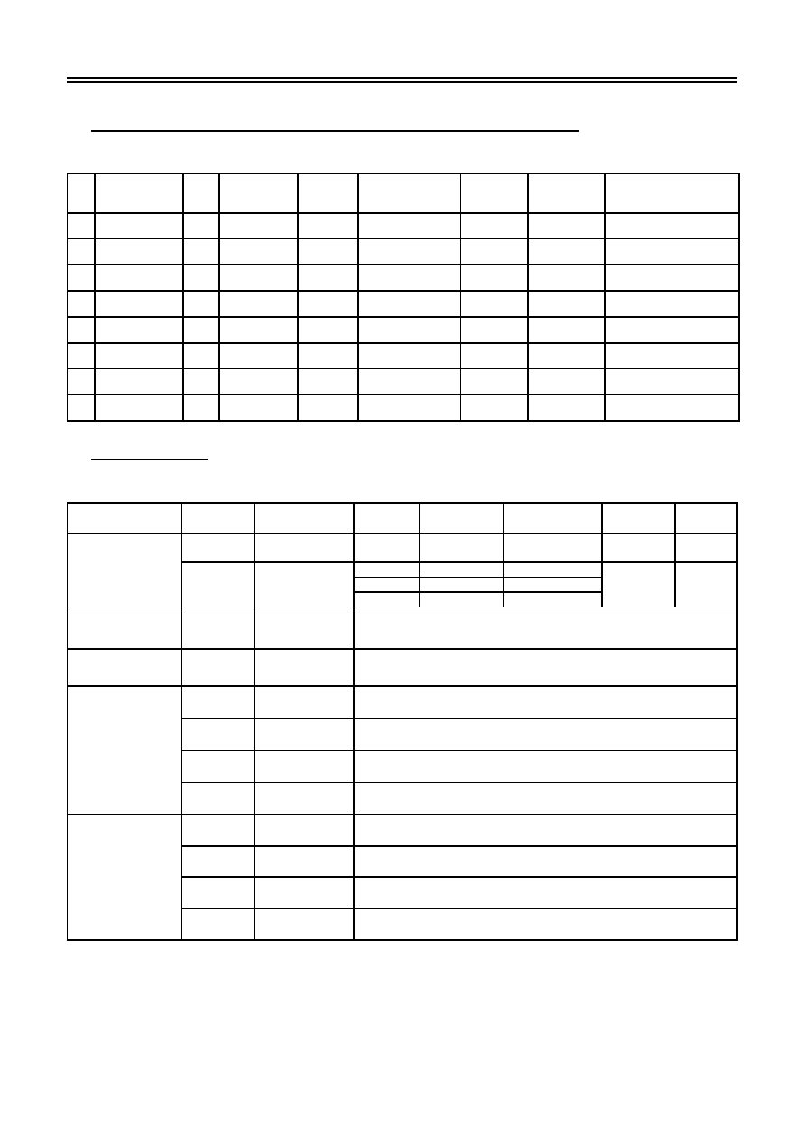
(9) S-8533A15AFT
Efficiency vs. Output current (CPH6303/CPH6403)
(10) S-8533A15AFT
Efficiency vs. Output current (Si3441DV/Si3442DV)
(11) S-8533A33AFT
Efficiency vs. Output current (CPH6303/CPH6403)
(12) S-8533A33AFT
Efficiency vs. Output current (Si3441DV/Si3442DV)
(13) S-8533A33AFT
Efficiency vs. Output current (CPH6302/CPH6402)
(14) S-8533A33AFT
Efficiency vs. Output current (Si3454DV/Si3455DV)
(15) S-8533A50AFT
Efficiency vs. Output current (CPH6302/CPH6402)
(16) S-8533A50AFT
Efficiency vs. Output current (Si3454DV/Si3455DV)
SYNCHRONOUS PWM CONTROL STEP-DOWN SWITCHING REGULATOR-CONTROLLERS
Rev.1.2
_00
S-8533 Series
Seiko Instruments Inc.
21
50
55
60
65
70
75
80
85
90
95
100
1
100
1000
10000
(mA)
50
55
60
65
70
75
80
85
90
95
100
1
100
1000
10000
(mA)
10
Output current
Output current
10
5.0 V
V
IN
= 2.7 V
5.0 V
V
IN
= 2.7 V
E
f
fi
c
i
ency
(%
)
E
f
fi
c
i
ency
(%
)
50
55
60
65
70
75
80
85
90
95
100
1
100
1000
10000
(mA)
50
55
60
65
70
75
80
85
90
95
100
1
100
1000
10000
(mA)
10
Output current
Output current
10
V
IN
= 4.0 V
4.95 V
7.0 V
V
IN
= 4.0 V
4.95 V
E
f
fi
c
i
ency
(%
)
E
f
fi
c
i
ency
(%
)
50
55
60
65
70
75
80
85
90
95
100
1
100
1000
10000
(mA)
50
55
60
65
70
75
80
85
90
95
100
1
100
1000
10000
(mA)
10
Output current
10
Output current
V
IN
= 4.95 V
10 V
10 V
V
IN
= 4.95 V
E
f
fi
c
i
ency
(%
)
E
f
fi
c
i
ency
(%
)
50
55
60
65
70
75
80
85
90
95
100
1
100
1000
10000
(mA)
50
55
60
65
70
75
80
85
90
95
100
1
100
1000
10000
(mA)
10
Output current
10
Output current
V
IN
= 6.0 V
16 V
10 V
7.5 V
V
IN
= 6.0 V
16 V
10 V
7.5 V
E
f
fi
c
i
ency
(%
)
E
f
fi
c
i
ency
(%
)
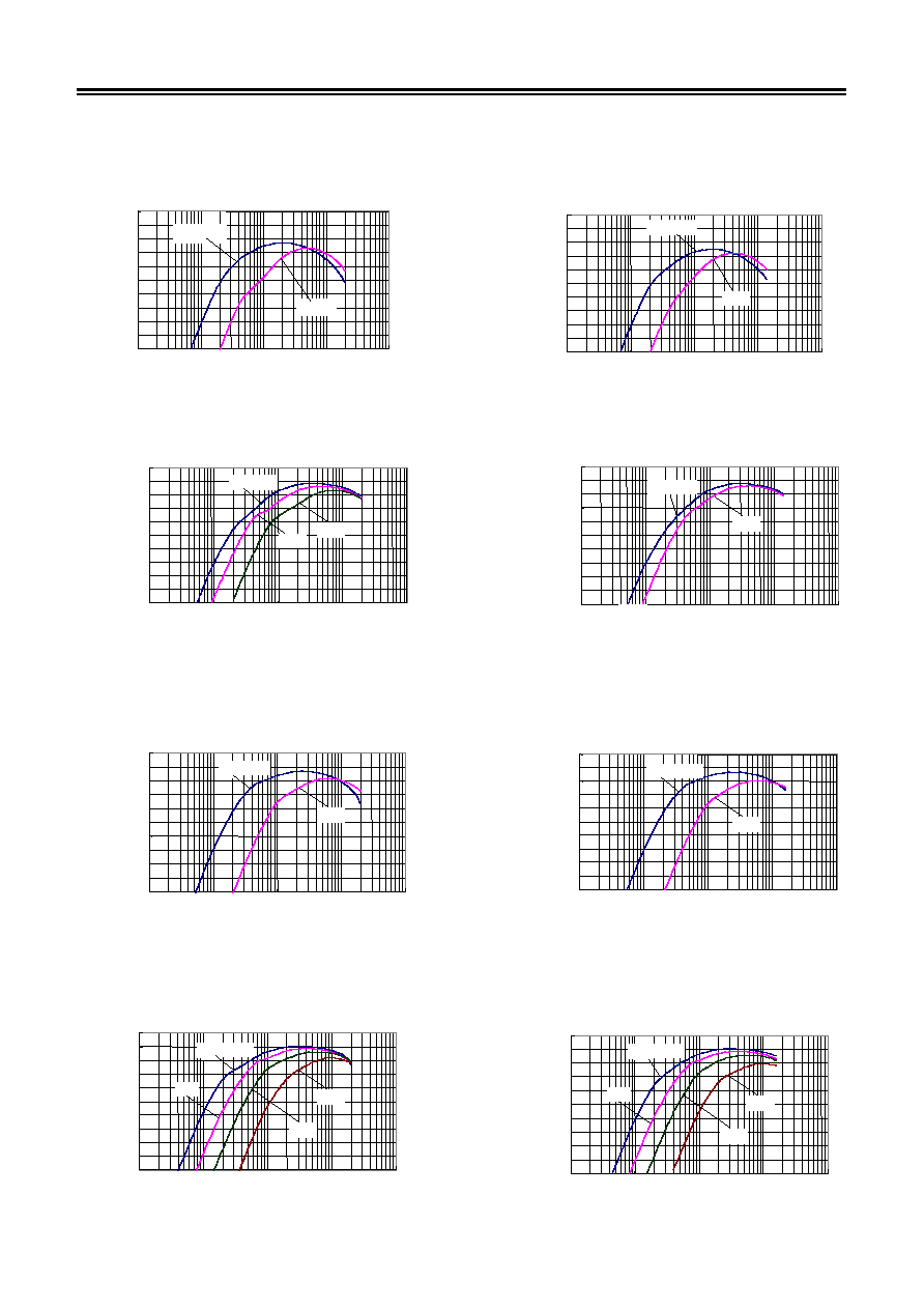
(17) S-8533A15AFT
Efficiency vs. Output current (CPH6303/CPH6403)
(18) S-8533A15AFT
Efficiency vs. Output current (Si3441DV/Si3442DV)
(19) S-8533A33AFT
Efficiency vs. Output current (CPH6303/CPH6403)
(20) S-8533A33AFT
Efficiency vs. Output current (Si3441DV/Si3442DV)
(21) S-8533A33AFT
Efficiency vs. Output current (CPH6302/CPH6402)
(22) S-8533A33AFT
Efficiency vs. Output current (Si3454DV/Si3455DV)
(23) S-8533A50AFT
Efficiency vs. Output current (CPH6302/CPH6402)
(24) S-8533A50AFT
Efficiency vs. Output current (Si3454DV/Si3455DV)
SYNCHRONOUS PWM CONTROL STEP-DOWN SWITCHING REGULATOR-CONTROLLERS
S-8533 Series
Rev.1.2
_00
Seiko Instruments Inc.
22
50
55
60
65
70
75
80
85
90
95
100
1
100
1000
10000
(mA)
50
55
60
65
70
75
80
85
90
95
100
1
10
100
1000
10000
(mA)
V
IN
= 4.95 V
7.0 V
Output current
Output current
10
13 V
V
IN
= 10 V
E
f
fi
c
i
ency
(%
)
E
f
fi
c
i
ency
(%
)
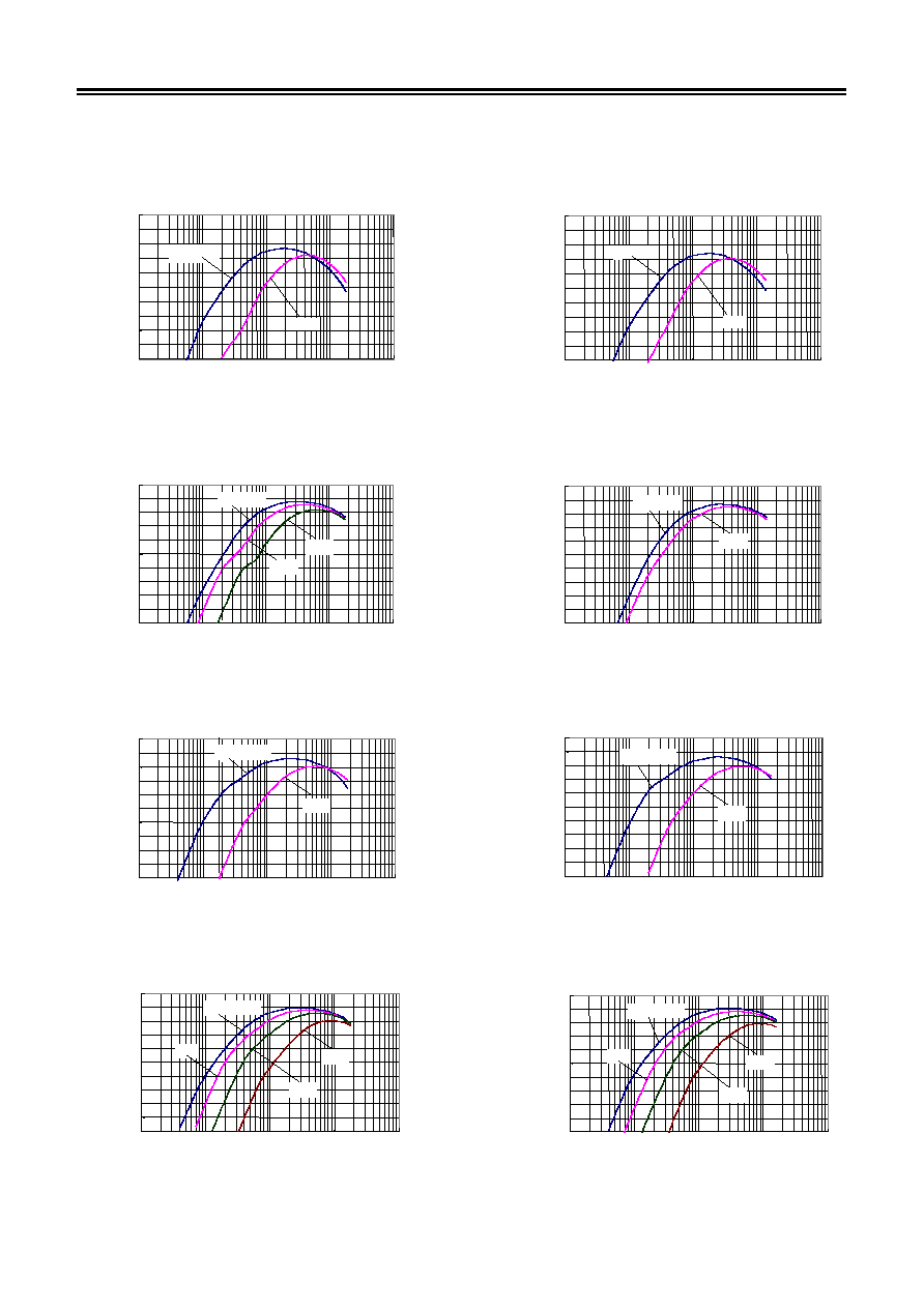
(25) S-8533A33AFT
Efficiency vs. Output current (CPH6303/CPH6403)
(26) S-8533A33AFT
Efficiency vs. Output current (CPH6302/CPH6402)
SYNCHRONOUS PWM CONTROL STEP-DOWN SWITCHING REGULATOR-CONTROLLERS
Rev.1.2
_00
S-8533 Series
Seiko Instruments Inc.
23
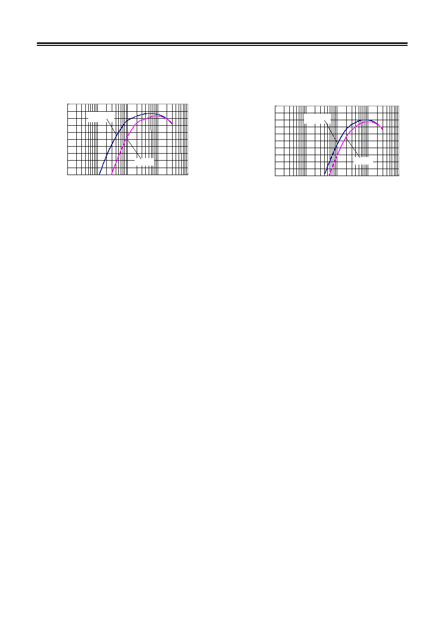
2. Ripple Voltage Characteristics
35
40
45
50
1
10
100
1000
10000
Output current (mA)
0
20
25
30
35
40
45
50
1
10
100
1000
10000
Output current (mA)
V
IN
= 2.7 V
5.0 V
R
i
pp
l
e
v
o
l
t
age V
r
(
m
V
)
15
10
5
0
5
R
i
pp
l
e
v
o
l
t
age V
r
(m
V
)
30
15
20
25
10
V
IN
= 2.7 V
5.0 V
0
35
40
45
50
1
10
100
1000
10000
Output current (mA)
0
35
40
45
50
1
10
100
1000
10000
Output voltage (mA)
5
10
15
20
25
30
30
5
10
15
20
25
V
IN
= 4.0 V
7.0 V
V
IN
= 4.0 V
4.95 V
4.95 V
R
i
pp
l
e
v
o
l
t
age V
r
(
m
V
)
R
i
pp
l
e
v
o
l
t
age V
r
(m
V
)
1
10
100
1000
10000
Output current (mA)
0
35
40
45
50
1
10
100
1000
10000
Output current (mA)
30
10
15
25
20
5
0
5
30
35
40
45
50
10
15
25
20
V
IN
= 4.95 V
10 V
V
IN
= 4.95 V
10 V
R
i
pp
l
e
v
o
l
t
age V
r
(
m
V
)
R
i
pp
l
e
v
o
l
t
age V
r
(m
V
)
0
5
10
30
40
45
50
1
10
100
1000
10000
Output current (mA)
0
5
50
1
10
100
1000
10000
Output current (mA)
20
35
25
15
10
15
20
25
30
35
40
45
V
IN
= 6.0 V
16 V
7.5 V
10 V
V
IN
= 6.0 V
16 V
7.5 V
10 V
Ri
p
p
l
e
v
o
lta
g
e
V
r
(
m
V
)
R
i
pp
l
e
v
o
l
t
age V
r
(m
V
)
(27) S-8533A15AFT
Ripple voltage vs. Output current (CPH6303/CPH6403)
(28) S-8533A15AFT
Ripple voltage vs. Output current (Si3441DV/Si3442DV)
(29) S-8533A33AFT
Ripple voltage vs. Output current (CPH6303/CPH6403)
(30) S-8533A33AFT
Ripple voltage vs. Output current (Si3441DV/Si3442DV)
(31) S-8533A33AFT
Ripple voltage vs. Output current (CPH6302/CPH6402)
(32) S-8533A33AFT
Ripple voltage vs. Output current (Si3454DV/Si3455DV)
(33) S-8533A50AFT
Ripple voltage vs. Output current (CPH6302/CPH6402)
(34) S-8533A50AFT
Ripple voltage vs. Output current (Si3454DV/Si3455DV)
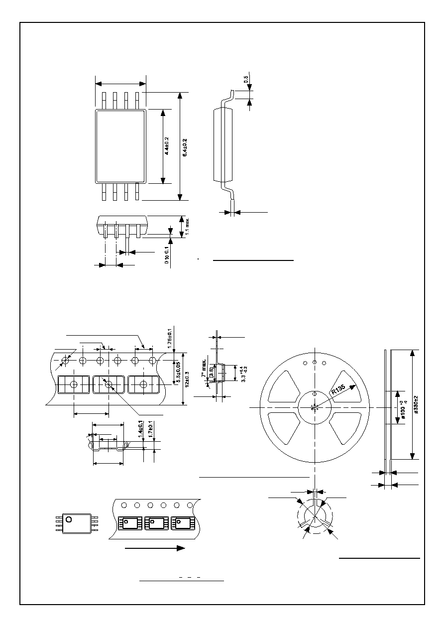
n 8-Pin TSSOP
FT008-A
Rev.3.1
021009
l Dimensions
0.65
0.2Ī0.1
3.00
+0.3
-0.2
1
4
5
8
0.17Ī0.05
No. : FT008-A-P-SD-1.1
l Tape Specifications
No. : FT008 A C SD-3.1
1
5
8
TB type
Feed direction
4
1.55Ī0.05
2.0Ī0.05
8.0Ī0.1
1.55
+0.1
-0
(6.9)
4.0
+0.4
-0.2
6.6
7į max.
4.0Ī0.1(50 pitches:200.0Ī0.3)
1.4Ī0.1
0.3Ī0.05
l Reel Specifications
No. : FT008-A-R-SD-3.1
13.4Ī1.0
Ý13Ī0.5
2Ī0.5
Ý21Ī0.8
1 reel holds 3000 ICs.
17.5Ī1.0
Enlarged drawing in the central part
Unit : mm

∑
The information described herein is subject to change without notice.
∑
Seiko Instruments Inc. is not responsible for any problems caused by circuits or diagrams described herein
whose related industrial properties, patents, or other rights belong to third parties. The application circuit
examples explain typical applications of the products, and do not guarantee the success of any specific
mass-production design.
∑
When the products described herein are regulated products subject to the Wassenaar Arrangement or other
agreements, they may not be exported without authorization from the appropriate governmental authority.
∑
Use of the information described herein for other purposes and/or reproduction or copying without the
express permission of Seiko Instruments Inc. is strictly prohibited.
∑
The products described herein cannot be used as part of any device or equipment affecting the human
body, such as exercise equipment, medical equipment, security systems, gas equipment, or any apparatus
installed in airplanes and other vehicles, without prior written permission of Seiko Instruments Inc.
∑
Although Seiko Instruments Inc. exerts the greatest possible effort to ensure high quality and reliability, the
failure or malfunction of semiconductor products may occur. The user of these products should therefore
give thorough consideration to safety design, including redundancy, fire-prevention measures, and
malfunction prevention, to prevent any accidents, fires, or community damage that may ensue.