
Rev.1.1
_70
Seiko Instruments Inc.
1
PWM Control & PWM/PFM Control High-Frequency
Step-Down Switching Regulator Controllers
S-8540/8541 Series
The S-8540/8541 Series is a family of CMOS step-down switching
regulator controllers with PWM control (S-8540) and PWM/PFM switchover
control (S-8541). These devices consist of a reference voltage source,
oscillation circuit, an error amplifier, phase compensation circuit, PWM
control circuit, current limit circuit. A high efficiency and large current
switching regulator is realized with the help of small external components
due to the high oscillation frequency, 300 kHz and 600 kHz.
The S-8540 provides low-ripple voltage, high efficiency, and excellent
transient characteristics which come form the PMW control circuit capable of
varying the duty ratio linearly from 0
% to 100 %, the optimized error
amplifier, and the phase compensation circuit.
The S-8541 operates under PWM control when the duty ratio is 29
% or
higher and operates under PFM control when the duty ratio is less than
29
% to ensure high efficiency over all load range.
These controllers serve as ideal main power supply units for portable
devices due to the high oscillation frequencies together with the small 8-Pin
MSOP package.
Features
∑ Oscillation frequency:
600 kHz (A & B series), 300 kHz (C & D series)
∑ Output voltage:
1.5 V to 6.0 V in steps of 0.1 V (A & C series)
Variable (Feed back) type is available.
∑ Output voltage precision: Ī2.0 %
∑ External components:
A transistor, a coil, a diode, and capacitors.
∑ Built-in PWM/PFM switchover control circuit(S-8541)
Duty
ratio:
29
% (PFM control)
29 to 100
% (PWM control)
∑ Current limit circuit:
Current is set by an external resistor R
SENSE
.
∑ Soft-start:
Time is set by an capacitor C
SS
and a resistor R
SS
.
∑ Power-off function
∑ Small package:
8-Pin MSOP
Package
∑ 8-Pin MSOP (Package drawing code: FN008-A)
Applications
∑ Power supplies for PDAs, electric organizers, and portable devices.
∑ Power supplies for audio equipment such as portable CD players and headphone stereos.
∑ Main or sub power supplies for notebook computers and peripheral equipment.
PWM Control & PWM/PFM Control High-Frequency Step-Down Switching Regulator-Controllers
S-8540/8541 Series
Rev.1.1
_70
Seiko Instruments Inc.
2
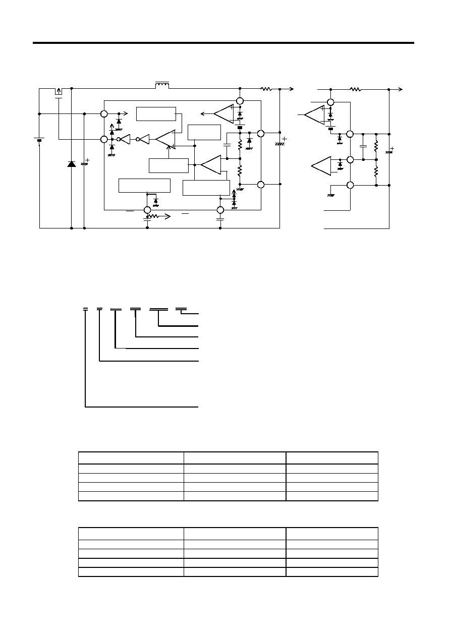
Block Diagram
SD
PWM or
PWM/PFM
switching control
Phase
compensation
circuit
Triangular wave
oscillation
circuit
VIN
L
EXT
Power-off soft start
circuit
V
IN
Pch Power
MOS FET
Power for IC
SENSE
PWM comparator
Error amplifier
C
IN
VSS
VOUT
C
OUT
R
SENSE
V
REF
=
=
=
=1.0V
125mV
CVREF
C
VL
ON/OFF
V
ON/OFF
CSS
R
SS
Voltage/current
reference
VSS
FB
C
FB
R
A
R
B
V
OUT
VOUT
R
SENSE
C
OUT
SENSE
125mV
Figure 1 Block diagram
Selection Guide
1. Product Name
S-854X X XX FN - XXX - T2
Tape specifications.
Package name abbreviation (8-Pin MSOP).
Product name abbreviation.
Output voltage (1.5 to 6.0 V), 00: Feed back type
A: Fixed output voltage, fosc
=600 kHz
B: Feed back type, fosc
=600kHz
C: Fixed output voltage, fosc
=300 kHz
D: Feed back0type, fosc
=300 kHz
0: PWM control
1: PWM/PFM switchover control
2. Product List (as of November 1, 2000)
2-1 A, B Series (oscillation frequency: 600 kHz)
Output Voltage (V)
S-8540XXXFN Series
S-8541XXXFN Series
1.8 V
S-8540A18FN-IAD-T2
S-8541A18FN-IGD-T2
2.5 V
S-8540A25FN-IAK-T2
S-8541A25FN-IGK-T2
3.3 V
S-8540A33FN-IAS-T2
S-8541A33FN-IGS-T2
Feed back (1.5 to 6.0)
S-8540B00FN-IMA-T2
S-8541B00FN-IMD-T2
2.2 C,D Series (oscillation frequency: 300 kHz)
Output Voltage (V)
S-8540XXXFN Series
S-8541XXXFN Series
1.8 S-8540C18FN-ICD-T2
S-8541C18FN-IID-T2
2.5 S-8540C25FN-ICK-T2
S-8541C25FN-IIK-T2
3.3 S-8540C33FN-ICS-T2
S-8541C33FN-IIS-T2
Feed back (1.5 to 6.0)
S-8540D00FN-IMB-T2
S-8541D00FN-IME-T2
When another output voltage product is needed, please contact SII sales office.

PWM Control & PWM/PFM Control High-Frequency Step-Down Switching Regulator-Controllers
Rev.1.1
_70
S-8540/8541 Series
Seiko Instruments Inc.
3
Pin Assignment
8-Pin MSOP
Top view
Figure 2
Absolute Maximum Ratings
(Ta
= 25įC, unless otherwise specified)
Item
Symbol
Ratings
Units
VIN pin voltage
V
IN
V
SS
-0.3 to V
SS
+12 V
CVREF pin voltage
V
CVREF
V
SS
-0.3 to V
IN
+0.3 V
ON/OFF pin voltage
V
ON/OFF
V
SS
-0.3 to V
SS
+12 V
FB pin voltage
*1
V
FB
V
SS
-0.3 to V
SS
+12 V
VOUT pin voltage
V
OUT
V
SS
-0.3 to V
SS
+12 V
SENSE pin voltage
V
SENSE
V
SS
-0.3 to V
SS
+12 V
EXT pin voltage
V
EXT
V
SS
-0.3 to V
IN
+0.3 V
EXT pin current
I
EXT
Ī100 mA
Power dissipation
P
D
300 mW
Operating temperature range
T
opr
-40 to 85
įC
Storage temperature range
T
stg
-40 to 125
įC
*1. Feed back type
Caution The absolute maximum ratings are rated values exceeding which the product could
suffer physical damage. These values must therefore not be exceeded under any
conditions.
Pin No. Pin Name
Function
1 VSS GND pin
2
EXT
Connection pin for external transistor
3
VIN
IC power supply pin
4 CVREF
Bypass capacitor connection pin for
reference voltage source
5
ON/ OFF
Power-off pin
Soft-start capacitor connection pin
∑ Normal operation (Step-down operation)
∑ All circuit halts (No step-down operation)
6
NC
(FB)
Fixed output pin; None connected
[Feed back type; Feed back pin]
7
VOUT Output voltage pin
8
SENSE Current limit detection pin
1
2
3
4
5
6
7
8

PWM Control & PWM/PFM Control High-Frequency Step-Down Switching Regulator-Controllers
S-8540/8541 Series
Rev.1.1
_70
Seiko Instruments Inc.
4
Electrical Characteristics
1. S-8540/41A,
C
(Ta
= 25 įC, unless otherwise specified)
Parameter Symbol
Conditions
Min.
Typ.
Max.
Units
Circui
t
Output voltage
*1
V
OUT
(E)
V
IN
= V
OUT
(S)
◊ 1.5
I
OUT
= 120 mA
V
OUT
(S)
◊ 0.980
V
OUT
(S) V
OUT
(S)
◊ 1.020
V 2
Input voltage
V
IN
-
2.5
-
10.0 V 1
Current consumption 1
I
SS1
V
IN
= V
OUT
(S)
◊ 1.5
S-8540/41AXX
-
180 300
ĶA
1
100
% duty ratio
S-8540/41CXX
-
140 240
Current consumption
during power off
I
SSS
V
ON/OFF
= 0 V
V
OUT
= V
OUT
(S)
◊ 0.95
-
-
1.0
ĶA
1
EXT pin output current
I
EXTH
V
IN
=10 V, V
EXT
= V
IN
-0.2 V
-32
-48
-
mA 1
I
EXTL
V
IN
=10 V, V
EXT
= 0.2 V
45 66 -
mA 1
Line regulation
V
OUT1
V
OUT
(S)
◊1.1 V
IN
10 V, I
OUT
= 120 mA
-
30 60
mV
2
Load regulation
V
OUT2
V
IN
=V
OUT
(S)
◊1.5, 10 ĶA I
OUT
150 mA
-
30 60
mV
2
Output voltage
temperature coefficient
V
Ta V
OUT
OUT
∑
V
IN
=V
OUT
(S)
◊1.5, I
OUT
= 120 mA
-40įC Ta 85įC
-
Ī100
-
ppm/
įC
2
S-8540/41AXX 510
600
690
kHz
2
Oscillation frequency
fosc
Measure waveform
at the EXT pin.
S-8540/41CXX 255
300
345
Maximum duty ratio
MaxDuty
Measure waveform at the EXT pin.
100
-
-
%
2
PWM/PFM-control
switch duty ratio
*2
PFM Duty
V
IN
= V
OUT
(S)
◊ 1.5, No load
19 29 39
%
2
Current limit detection
voltage
V
SENSE
V
IN
= V
OUT
(S)
◊ 1.5,
Measure waveform at the EXT pin.
100 125 150
mV
1
SENSE pin input
current
I
SENSE
V
IN
= V
OUT
(S)
◊ 1.5, V
SENSE
= V
IN
-0.1 V
6.7 11.2 16.8
ĶA
1
Power-Off pin
V
SH
V
IN
= V
OUT
(S)
◊ 1.5, Judge V
OUT
(S)
◊ 0.98.
2.3
-
-
V 2
input voltage
V
SL
V
IN
= V
OUT
(S)
◊ 1.5, Judge CVREF pin "L".
-
-
0.3 V 1
Power-Off pin
I
SH
V
IN
= V
OUT
(S)
◊ 1.5, V
ON/OFF
= V
OUT
-0.1
-
0.1
ĶA
1
input leakage current
I
SL
V
IN
= V
OUT
(S)
◊ 1.5, V
ON/OFF
= 0 V
-0.1
-
0.1
ĶA
1
Soft-Start time
T
SS
Time until V
OUT
(E) reaches 90
%
or higher of the setting
7.0 12.0 17.0
ms
2
Efficiency EFFI
-
-
90
-
%
2
Condition: Recommended parts are used unless otherwise specified.
V
IN
=V
OUT
(S)
◊1.5(V), I
OUT
=120(mA) (When V
OUT
(S)
1.6 V, then V
IN
= 2.5 V)
*1. V
OUT
(S) : Specified output voltage value
V
OUT
(E) : Actual output voltage value
*2. Applied to the S-8541 series only
External components
Coil (L):
Sumida Electric Co., Ltd. CDRH6D28-100
Diode (SD):
Panasonic MA2Q737 (Schottky diode)
Output capacitor (C
OUT
): Nichicon Corporation F93 (16 V, 47
ĶF, tantalum)
Input
capacitor
(C
IN
):
Nichicon Corporation F93 (16 V, 47
ĶF, tantalum)
Transistor
(P
SW
):
Toshiba Corporation 2SA1213
Base resistor (R
b
): 100
m
Base capacitor (C
b
): 2200
pF
C
VL
: 1.0
ĶF
C
SS
: 0.047
ĶF
R
SS
: 220
k
R
SENSE
: 100
m
Note: Line regulation and load regulation may change greatly due to GND wiring when V
IN
is high.
In the S-8540 series (PWM control), a state in which the duty ratio 0
% continues for several clocks may occur when the input voltage
is high and the output current is low. In this case, the operation changes to the pseudo PFM mode, but the ripple voltage hardly
increases.

PWM Control & PWM/PFM Control High-Frequency Step-Down Switching Regulator-Controllers
Rev.1.1
_70
S-8540/8541 Series
Seiko Instruments Inc.
5
2. S-8540/41B,D
(Ta=25įC,unless otherwise specified)
Parameter Symbol
Conditions
Min.
Typ.
Max.
Units
Circuit
Output voltage
*1, *2
V
OUT
(E)
V
IN
= 4.5 V
I
OUT
= 120 mA
V
OUT
(S)
◊0.980
V
OUT
(S)
=3.000
V
OUT
(S)
◊1.020
V 4
Input voltage
V
IN
-
2.5
-
10.0 V 3
Current consumption 1
I
SS1
V
IN
= 4.5 V
S-8540/41B00
-
180 300
ĶA
3
100
% duty ratio
S-8540/41D00
-
140 240
Current consumption
during power off
I
SSS
V
ON/OFF
= 0 V
V
OUT
= V
OUT
(S)
◊ 0.95
-
-
1.0
ĶA
3
EXT pin output current
I
EXTH
V
IN
=10 V, V
EXT
= V
IN
-0.2 V
-32
-48
-
mA 3
I
EXTL
V
IN
=10 V, V
EXT
= 0.2 V
45 66 -
mA 3
Line regulation
V
OUT1
3.3
V
IN
10 V, I
OUT
=120 mA
-
30 60
mV
4
Load regulation
V
OUT2
10
ĶA I
OUT
150 mA
-
30 60
mV
4
Output voltage
temperature coefficient
V
Ta V
OUT
OUT
∑
V
IN
=V
OUT
(S)
◊1.5, I
OUT
=120 mA
-40įC Ta 85įC
-
Ī100
-
ppm/
įC
4
Oscillation frequency
fosc
Measure waveform at
S-8540/41B00
510
600
690
kHz
4
the
EXT
pin.
S-8540/41D00
255
300
345
Maximum duty ratio
MaxDuty
Measure waveform at the EXT pin.
100
-
-
%
4
PWM/PFM-control
switch duty ratio
*3
PFM Duty
V
IN
= V
OUT
(S)
◊ 1.5 V, No load
19 29 39 %
4
Current limit detection
voltage
V
SENSE
V
IN
= 4.5 V, Measure waveform at the EXT pin.
100 125 150 mV
3
SENSE pin input
current
I
SENSE
V
IN
= 4.5 V, V
SENSE
= V
IN
-0.1 V
6.7 11.2 16.8 ĶA
3
Power-Off pin
V
SH
V
IN
= 4.5 V, Judge V
OUT
(S)
◊ 0.98.
2.3
-
-
V 4
input voltage
V
SL
V
IN
= 4.5 V, Judge CVREF pin "L".
-
-
0.3 V 3
Power-Off pin
I
SH
V
IN
= 4.5 V, V
ON/OFF
= V
OUT
-0.1
-
0.1
ĶA
3
input leakage current
I
SL
V
IN
= 4.5 V, V
ON/OFF
= 0 V
-0.1
-
0.1
ĶA
3
Soft-Start time
T
SS
Time until V
OUT
(E) reaches 90
%
or higher of the setting
7.0 12.0 17.0
ms
4
Efficiency EFFI
-
-
90
-
%
4
Condition:
Connect recommended parts unless otherwise specified. V
IN
=V
OUT
(S)
◊1.5(V), I
OUT
=120(mA)
*1. V
OUT
(S) : Specified output voltage value
V
OUT
(E) : Actual output voltage value
*2. The typical value (specified output voltage value) is V
OUT
(S)
= 1+R
A
/R
B
=3.0(V). See "Output Voltage adjustment".
*3. S-8541 series only
External components
Coil (L):
Sumida Electric Co., Ltd. CDRH6D28-100
Diode (SD):
Panasonic MA2Q737 (Schottky diode)
Output capacitor (C
OUT
): Nichicon Corporation F93 (16 V, 47
ĶF, tantalum)
Input
capacitor
(C
IN
):
Nichicon Corporation F93 (16 V, 47
ĶF, tantalum)
Transistor
(P
SW
):
Toshiba Corporation 2SA1213
Base resistor (R
b
): 100
m
Base capacitor (C
b
): 2200
pF
C
VL
: 1.0
ĶF
C
SS
: 0.047
ĶF
R
SS
: 220
k
R
SENSE
: 100
m
R
A
: 200
k
R
B
: 100
k
C
FB
: 50
pF
Note: Line regulation and load regulation may change greatly due to GND wiring when V
IN
is high.
In the S-8540 series (PWM control), a state in which the duty ratio 0
% continues for several clocks may occur when the input voltage
is high and the output current is low. In this case, the operation changes to the pseudo PFM mode, but the ripple voltage hardly
increases.

PWM Control & PWM/PFM Control High-Frequency Step-Down Switching Regulator-Controllers
S-8540/8541 Series
Rev.1.1
_70
Seiko Instruments Inc.
6
Measurement Circuits
1
VSS
ON/OFF
EXT
SENSE
VOUT
VIN
CVREF
A
A
A
A
A
A
C
VL
C
IN
L
SD
P
SW
C
b
R
b
V
IN
C
IN
CVREF
R
SENSE
C
SS
C
OUT
R
SS
V
ON/OFF
2
+
+
VSS
ON/OFF
EXT
SENSE
VOUT
VIN
C
VL
3
A
A
A
A
A
A
CVREF
C
IN
VSS
ON/OFF
EXT
FB
SENSE
VOUT
VIN
C
VL
R
A
R
B
C
FB
L
SD
P
SW
C
b
R
b
V
IN
C
IN
CVREF
R
B
R
SENSE
C
FB
R
A
C
SS
C
OUT
R
SS
V
ON/OFF
4
+
+
VSS
ON/OFF
EXT
FB
SENSE
VOUT
VIN
C
VL
Figure 3
PWM Control & PWM/PFM Control High-Frequency Step-Down Switching Regulator-Controllers
Rev.1.1
_70
S-8540/8541 Series
Seiko Instruments Inc.
7
Operation
1. Step-down DC-DC converter
1.1 PWM Control (S-8540 Series)
The S-8540 series consists of pulse width modulation (PWM) DC/DC converters. In conventional pulse
frequency modulation (PFM) DC/DC converters, pulses are skipped when they operate at low output load
current, causing the variation in the ripple frequency and the increase in the ripple voltage of the output
voltage both of which constitute inherent drawbacks to those converters.
In the S-8540 series the pulse width varies in the range from 0
% to 100 % according to the load current,
yet ripple voltage produced by the switching can easily be removed by a filter since the switching
frequency is always constant. These converters thus provide a low-ripple voltage over wide range of input
voltage and load current.
1.2 PWM/PFM Switchover Control (S-8541 Series)
The S-8541 series consists of DC/DC converters capable of automatic switching between the pulse width
modulation (PWM) and the pulse frequency modulation (PFM) according to the load current and is
characterized by its low current consumption.
In a region of high output load current, the S-8541 operates under PWM control where the pulse width
duty varies from 29
% to 100 % to realize low ripple power source.
In a region of low output load current, the converter is switched to PFM control where pulses having fixed
width and the duty of 29
% are skipped depending on the load current, and are sent to the switching
transistor. The oscillation circuit thus enters intermittent oscillation, the current consumption is reduced
and efficiency lowering at low load is avoided. For output load current especially in the region of 100
ĶA, a
high efficiency DC/DC converter can be realized.
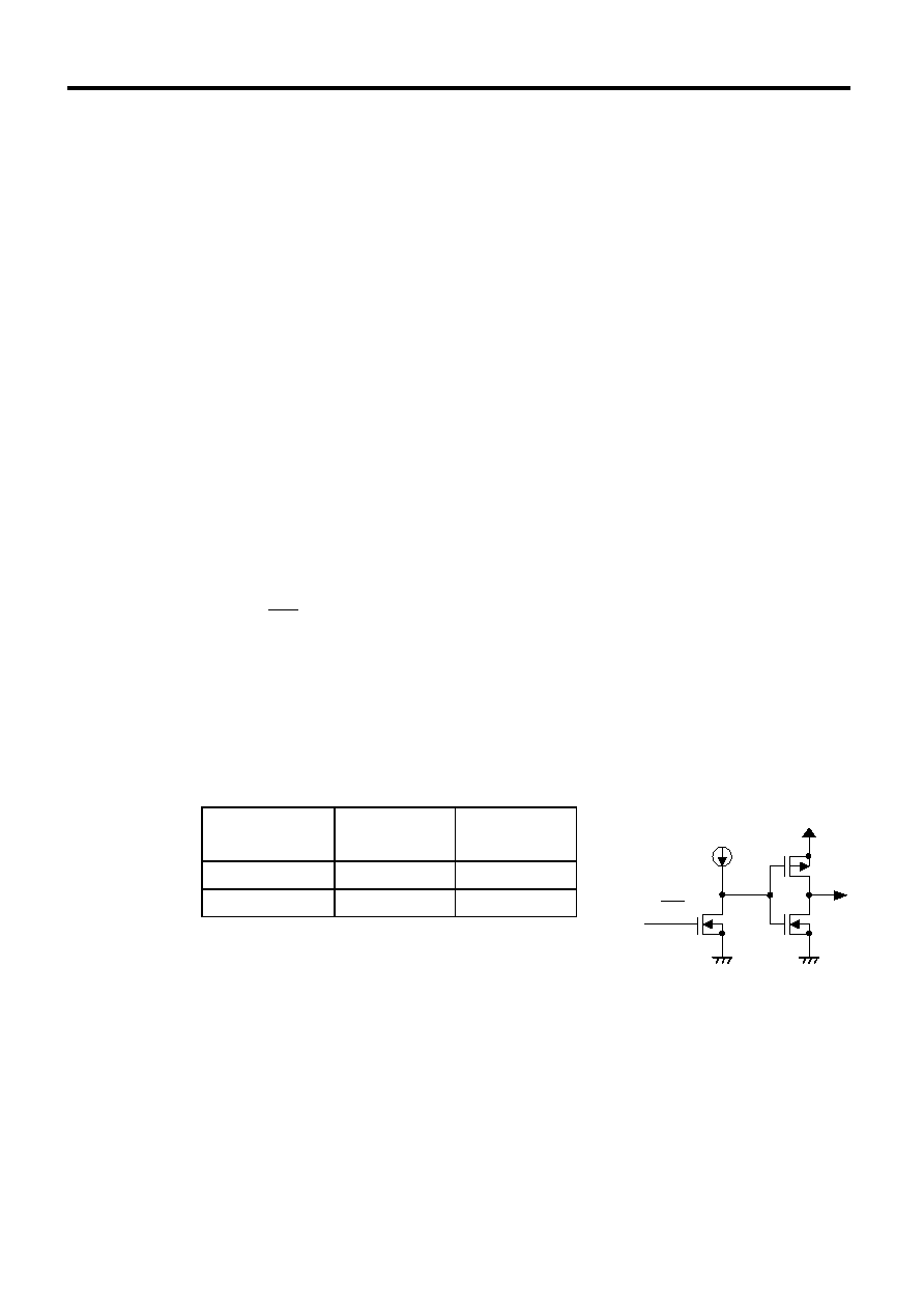
2. Power-Off Pin (ON/ OFF Pin)
This pin deactivates and activates the step-down operation. When the power-off pin is set to "L", the
voltage of the EXT pin goes to V
IN
level to shut off the switching transistor. All the internal circuits stop,
and substantial saving in current consumption is achieved.
The power-off pin is configured as shown in the figure 4. Since pull-up or pull-down is not performed
internally, operation where the power-off pin is in a floating state should be avoided. Application of voltage
of 0.3 V to 1.8 V to the pin should also be avoided lest the current consumption increases. When the
power-off pin is not used, it should be connected to the VIN pin.
Power-Off Pin
CR Oscillation
Circuit
Output Voltage
"
H" Active
Set
value
"
L" Non-active
OPEN
Figure 4
VSS
VIN
ON/
OFF
PWM Control & PWM/PFM Control High-Frequency Step-Down Switching Regulator-Controllers
S-8540/8541 Series
Rev.1.1
_70
Seiko Instruments Inc.
8
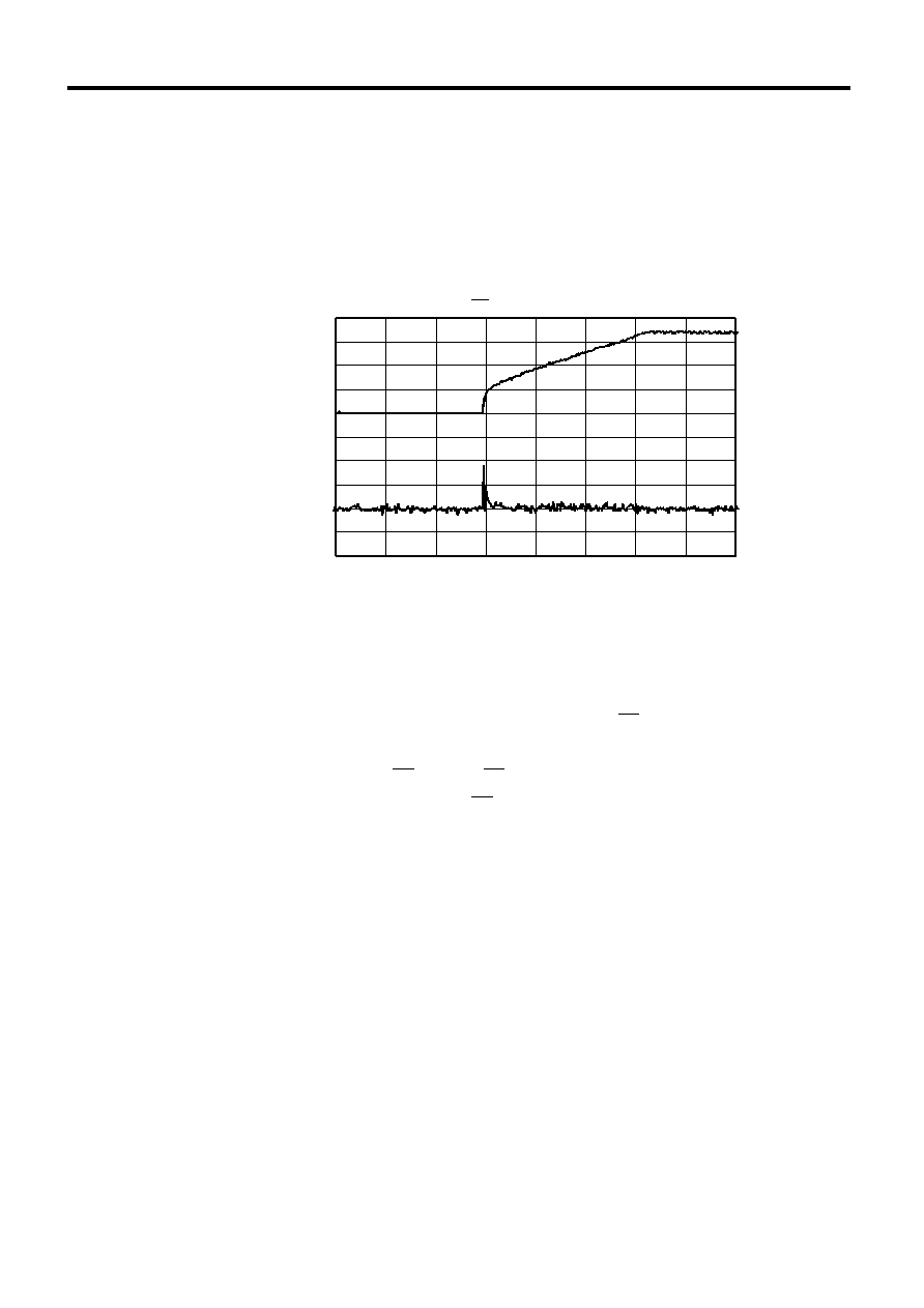
3. Soft-start
Function
The S-8540/8541 series has a built-in soft-start circuit. This circuit enables the output voltage to rise
gradually over the specified soft-start time to suppress the overshooting of the output voltage and the
rush current from the power source when the power is switched on or the power-off pin is set to "H".
The soft-start function of this IC, however, can not suppress rush current to the load completely.
(See figure 5. The rush current is affected by the input voltage and the load. Please evaluate the rush
current under the actual test condition.)
time(1 ms/div)
V
OUT
(1 V/div)
Push current
(0.5 A/div)
0 V
3.0 V
0 A
1 A
S-8540A33FN(V
IN
= V
ON / OFF
= 0 5 V)
Figure 5 Wave form of Output Voltage and Rush Current at Soft-start
The soft-start function of the IC is achieved by raising internal reference voltage gradually, which is
caused by the raising of power-off pin voltage through RC components (R
SS
and C
SS
) connected to
power-off pin.
A soft-start time (T
SS
) is changed by R
SS
, C
SS
and the input voltage V
ON/OFF
to R
SS
.
T
SS
is calculated from the following formula:
T
SS [ms]
=R
[k
]
◊ C
[
ĶF]
◊ In(V
ON/OFF
[V]/(V
ON/OFF
[V]
-1.8))
Example : When R
SS
=220 k, C
SS
=0.047 ĶF, V
ON/OFF
=2.7 V , then T
SS
=11.4 ms
PWM Control & PWM/PFM Control High-Frequency Step-Down Switching Regulator-Controllers
Rev.1.1
_70
S-8540/8541 Series
Seiko Instruments Inc.
9
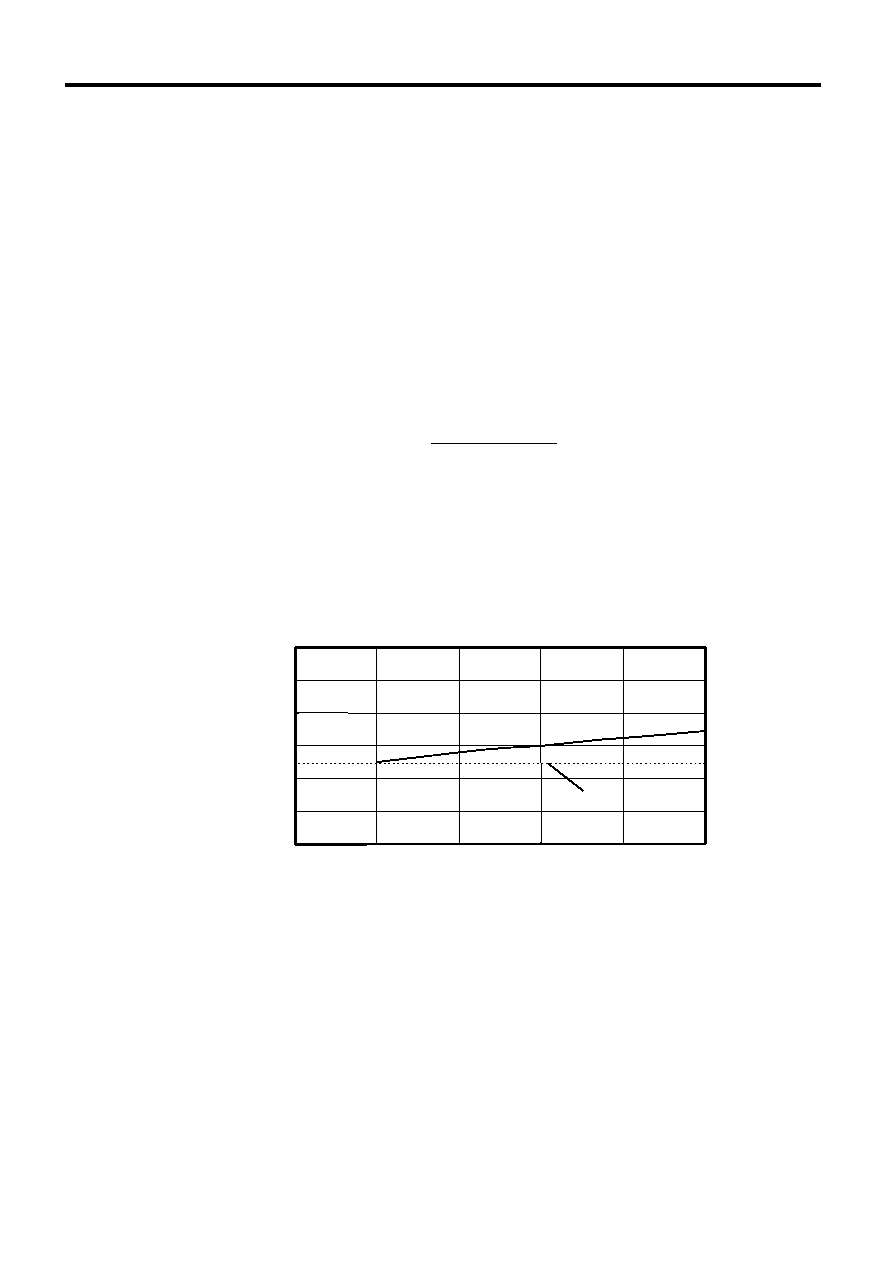
4. Current Limit Circuit
The S-8540/41 series contains a current limit circuit.
The current limit circuit is designed to prevent thermal destruction of external transistors due to overload
or magnetic saturation of the coil.
The current limit circuit can be enabled by inserting a sense resistor (R
SENSE
) between the external coil
and the output pin VOUT, and connecting the node for the sense resistor and the coil to the SENSE pin.
A current limit comparator in the IC is used to check whether the voltage between the SENSE pin and
VOUT pin reaches the current limit detection voltage (V
SENSE
=125 mV(typ.)). The current flowing through
the external transistor is limited by turning it off during the left time of the oscillation period after detection.
The transistor is turned on again at the next clock and current limit detection resumes. If the overcurrent
state still persists, the current limit circuit operates again, and the process is repeated. If the overcurrent
state is eliminated, the normal operation resumes. Slight overshoot occurs in the output voltage when the
overcurrent state is eliminated.
I
Limit
(current limit setting value) is calculated by the following formula:
I
Limit
(current limit setting value)
=
Vsense( 125 mV)
Rsense
=
If the change with time of the current flowing through the sense resistor is higher than the response speed
of the current limit comparator in the IC, the actual current limit value becomes higher than the I
Limit
(current limit setting value) calculated by the above formula. When the voltage difference between VIN
and VOUT is large, the actual current limit value increases since the change with time of the current
flowing through the sense resistor becomes large.
V
IN
vs. I
peak
in the overcurrent state
V
IN
vs. I
peak
0.0
0.5
1.0
1.5
2.0
2.5
3.0
2.5 4.0 5.5 7.0 8.5 10.0
V
IN
(V)
I
peak
(A)
(IC:S-8540A33FN, coil:CDRH6D28-100, R
SENSE
:100 m
)
1.25 A
Figure 6 l
peak
change by input voltage
When the output voltage is approximate 1.0 V or less, the load short-circuit protection does not work,
since the current limit circuit does not operate.
When the current limit circuit is not used, remove the sense resistor and connect the SENSE pin to the
VSS or VOUT pin.
5. 100
%
%
%
% Duty Cycle
The S-8540/8541 series operates up to the maximum duty cycle of 100
%. The switching transistor is
kept on continuously to supply current to the load, when the input voltage falls below the preset output
voltage value. The output voltage in this case is equal to the subtraction of lowering causes by DC
resistance of the coil and on resistance of the switching FET from the input voltage.
Even when the duty cycle is 100
%, the current limit circuit works when overcurrent flows.

PWM Control & PWM/PFM Control High-Frequency Step-Down Switching Regulator-Controllers
S-8540/8541 Series
Rev.1.1
_70
Seiko Instruments Inc.
10
Selection of Series Products and Associated External Components
1. Selecting a product
The S-8540/41 series is classified into eight types according to the way of control (PWM and PWM/PFM
switching), the oscillation frequencies, and output voltage settings (fixed and feed back). Please select
the type that suits your needs best by taking the advantage described below into account.
(1) Control method:
Two different control methods are available: PWM control (S-8540 Series) and PWM/PFM
switching control (S-8541 Series).
(2) Oscillation frequencies:
Two oscillation frequencies -- 600 kHz (A & B Series) and 300 kHz (C & D Series) -- are
available.
Because of their high oscillation frequency, the products in the A and B Series allow the use of
small size inductors since the peak current decreases when the same load current flows. In
addition, they can also be used with small output capacitors. These outstanding features make
the A & B series ideal for downsized devices.
On the other hand, the C & D series, having lower oscillation frequency, are characterized by
small self-consumption current and excellent efficiency under light load.
(3) Output voltage setting:
Two different types are available: fixed output (A & C series) and feed back type (B & D
series).
The table below provides a rough guide for selecting a product depending on the requirements
of the application. Choose the product that has the best score ( ).
S-8540
S-8541
A B C D A B C D
The set output voltage is fixed (1.5 to 6.0 V)
Set an output voltage freely (1.5 to 6.0 V)
The efficiency at light load (less than 10 mA) is
important.
The efficiency at 100 mA or more is important.
Low-ripple voltage is important.
Use of small external parts is Important.
The symbol "
" denotes an indispensable condition, while the symbol " " indicates that the
corresponding series has superiority in that aspect. The symbol " " indicates particularly high score.
2. Inductor
The inductance value greatly affects the maximum output current I
OUT
and the efficiency
.
As the Inductance is reduced gradually, the peak current Ipk increases, and the output current I
OUT
reaches the maximum at a certain Inductance value. As the Inductance is made even smaller, I
OUT
begins
to decrease since the current drivability of the switching transistor becomes insufficient.
Conversely, as the Inductance is increased, the loss in the switching transistor due to Ipk decreases, and
the efficiency reaches the maximum at a certain Inductance value. As the Inductance is made even
larger, the efficiency degrades since the loss due to the series resistance of the inductor increases.

PWM Control & PWM/PFM Control High-Frequency Step-Down Switching Regulator-Controllers
Rev.1.1
_70
S-8540/8541 Series
Seiko Instruments Inc.
11
When the inductance is large in an S-8540/41 series product, the output voltage may grow unstable in
some cases, depending on the conditions of the input voltage, output voltage, and the load current.
Perform sufficient evaluation under the actual condition and decide an optimum inductance.
In many applications, an inductance of 10
ĶH for A/B series and 22 ĶH for C/D series will yield the best
characteristics of the S-8540/41 series in a well balanced manner.
When choosing an inductor, attention to its allowable current should be paid since the current over the
allowable value will cause magnetic saturation in the inductor, leading to a marked decline in efficiency.
An inductor should therefore be selected so as not the peak current I
PK
to surpass its allowable current.
The peak current I
PK
is represented by the following equation in non-continuous operation mode:
I
I
V
(V
V )
2 fosc L V
PK
OUT
OUT
IN
OUT
IN
=
+
◊
-
◊
◊ ◊
Where fosc is the oscillation frequency and L is the inductance value of the inductor.
3. Diode
The diode should meet the following conditions:
The forward voltage is low (Schottky barrier diode is recommended).
The switching speed is high (50 ns max.).
The reverse breakdown voltage is higher than V
IN
.
The current rating is larger than I
PK
.
4. Capacitors
4.1 Input/output capacitors (C
IN
, C
OUT
)
The capacitor inserted in the input side (C
IN
) serves to reduce the power impedance and to average the
input current for better efficiency. The C
IN
value should be selected according to the impedance of the
power supply. It should be 47 to 100
ĶF, although the actual value depends on the impedance of the
power source used and load current value.
For the output side capacitor (C
OUT
), select a large capacitance with low ESR (Equivalent Series
Resistance) to smoothen the ripple voltage. When the input voltage is extremely high or the load current
is extremely large, the output voltage may become unstable. In this case the unstable area will become
narrow by selecting a large capacitance for an output side capacitor. A tantalum electrolytic capacitor is
recommended since the unstable area widens when a capacitor with a large ESR, such as an aluminum
electrolytic capacitor, or a capacitor with a small ESR, such as a ceramic capacitor, is chosen. The range
of the capacitance should generally be 47
ĶF to 100 ĶF.
4.2 Internal power source stabilization capacitor (C
VL
)
The main circuits of the IC work on an internal power source connected to the CVREF pin. The C
VL
is a
bypass capacitor for stabilizing the internal power source. C
VL
should be a 1
ĶF ceramic capacitor and
should be wired in a short distance and at a low impedance.
5. External Switching Transistors
The S-8540/41 series can work with an enhancement (Pch) MOSFET or a bipolar (PNP) transistor as an
external switching transistor.
5.1 Enhancement
MOSFET
The EXT pin of the S-8540/41 series can directly drive the Pch power MOSFET with a gate capacity of
approximate 1200 pF.
When a Pch power MOSFET is chosen, efficiency will be 2 to 3
% higher than that achieved by a PNP
bipolar transistor since the MOSFET switching speed is faster than that of the bipolar transistor and
power loss due to the base current is avoided,.
The important parameters in selecting a Pch power MOSFET are the threshold voltage, breakdown
voltage between gate and source, breakdown voltage between drain and source, total gate capacity, on-
resistance, and the current ratings.

PWM Control & PWM/PFM Control High-Frequency Step-Down Switching Regulator-Controllers
S-8540/8541 Series
Rev.1.1
_70
Seiko Instruments Inc.
12
The EXT pin swings from voltage V
IN
to V
SS
. When the input voltage is low, a MOS FET with a low
threshold voltage has to be used so that the MOSFET will turn on as required. When, conversely, the
input voltage is high, select a MOSFET whose gate-source breakdown voltage is higher than the input
voltage by at least several volts.
Immediately after the power is turned on, or the power is turned off (that is, when the step-down operation
is terminated), the input voltage is applied across the drain and the source of the MOSFET. The transistor
therefore needs to have drain-source breakdown voltage that is also several volts higher than the input
voltage.
The total gate capacity and the on-resistance affect the efficiency.
The power loss for charging and discharging the gate capacity by switching operation will affect the
efficiency at low load current region more when the total gate capacity becomes larger and the input
voltage becomes higher. If the efficiency at low load is a matter of concern, select a MOSFET with a
small total gate capacity.
In regions where the load current is high, the efficiency is affected by power loss caused by the on-
resistance of the MOSFET. If the efficiency under heavy load is particularly important in the application,
choose a MOSFET having on-resistance as low as possible.
As for the current rating, select a MOSFET whose maximum continuous drain current rating is higher
than the peak current I
PK
.
5.2 PNP Bipolar Transistor
Figure 7 shows a circuit diagram using Toshiba Corporation 2SA1213-Y for the bipolar transistor (PNP).
Using a bipolar transistor, the driving capacity for increasing the output current is determined by the h
FE
value and the R
b
value.
V
IN
EXT
2SA1213-Y
VIN
R
b
C
b
Figure 7
The Rb value is given by the following equation:
EXTL
b
IN
b
I
0.4
I
0.7
V
R
-
-
=
Calculate the necessary base current Ib using the h
FE
value of the bipolar transistor from the relation, I
b
=
I
PK
/h
FE
, and select a smaller value for R
b
which is calculated from the above equation.
A small R
b
value will certainly contribute to increase the output current, but it will also decrease the
efficiency. Determine the optimum value through experiment since the base current flows as pulses and
voltage drop may takes place due to the wiring resistance and so on.
In addition, if speed-up capacitor C
b
is inserted in parallel with resistance R
b
, as shown in figure 7, the
switching loss will be reduced, leading to a higher efficiency.
Select a C
b
value by using the following equation :
0.7
fosc
R
2
1
C
b
b
◊
◊
◊
Adjust the optimum C
b
value, however, through experiment since the optimum C
b
value differs depending
upon the characteristics of the bipolar transistor.

PWM Control & PWM/PFM Control High-Frequency Step-Down Switching Regulator-Controllers
Rev.1.1
_70
S-8540/8541 Series
Seiko Instruments Inc.
13
Standard Circuits
(1) Fixed output voltage (Pch MOSFET)
L
SD
R
SENSE
Tr
V
IN
C
IN
SENSE
+
-
V
REF
=1.0 V
PWM,PWM/PFM
switching control
circuit
Power-off soft start
circuit
125mV
Error amplifier
PWM comparator
Triangular wave
oscillation circuit
Phase
compensation
circuit
Power for IC
VIN
EXT
+
-
+
-
C
OUT
VSS
VOUT
CVREF
V
ON/OFF
ON/OFF
One point ground
Voltage/current
reference
Figure 8 Fixed output voltage
(2) Feed back type (Pch MOSFET)
L
SD
R
SENSE
Tr
V
IN
C
IN
SENSE
+
-
V
REF
=1.0 V
125mV
VIN
EXT
+
-
+
-
C
OUT
VSS
VOUT
C
FB
R
B
R
A
FB
PWM, PWM/PFM
switching control
circuit
Power-off soft start
circuit
Error amplifier
PWM comparator
Triangular wave
oscillation circuit
Phase
compensation
circuit
Power for IC
Voltage/current
reference
CVREF
V
ON/OFF
ON/OFF
One point ground
Figure 9 External setting output voltage
Caution The above connections and values will not guarantee correct operation. Before setting these
values, perform sufficient evaluation on the application to be actually used.

PWM Control & PWM/PFM Control High-Frequency Step-Down Switching Regulator-Controllers
S-8540/8541 Series
Rev.1.1
_70
Seiko Instruments Inc.
14
Output voltage adjustment
The output voltage can be adjusted or changed in the output voltage setting range (1.5 to 6.0 V) by adding
external resistors (R
A
, R
B
) and a capacitor (C
FB
) in the S-8540/41B00AFN and S-8540/41D00AFN series.
Temperature gradient can be given by inserting a thermistor in series to R
A
and R
B
.
R
A
+ R
B
must be equal to or less than 2 M
and the ratio of R
A
to R
B
should be set so that the FB pin is 1.0 V.
Add a capacitor (C
FB
) in parallel to the external resistor (R
A
) to prevent unstable operation like output oscillation.
Set the C
FB
so that f
= 1/(2◊C
FB
◊R
A
) is 0.1 to 20 kHz (normally 10 kHz).
Example: When V
OUT
=3.0 V, R
A
=200 k, R
B
=100 k, then C
FB
=100 pF
The precision of output voltage (V
OUT
) determined by the resistors (R
A
, R
B
) is affected by the precision of the
voltage at the FB pin (1 V
Ī2.0 %), the precision of external resistors R
A
and R
B
, current input to the FB pin, and IC
power supply voltage V
DD
.
Suppose that the FB pin input current is 0 nA, and that the maximum absolute values of the external resistors R
A
and R
B
are R
A
max. and R
B
max, and the minimum absolute values of the external resistors R
A
and R
B
are R
A
min. and R
B
min., and that the output voltage shift due to the V
DD
voltage dependency is
V, the minimum value
V
OUT
min. and maximum value V
OUT
max. of the output voltage V
OUT
variation is calculated by the following
formula:
V
OUT
min.
= (1+ ) ◊ 0.98 - V [V]
V
OUT
max.
= (1+ ) ◊ 1.02 + V [V]
The precision of the output voltage V
OUT
cannot be made lower than the precision of the IC output voltage without
adjustment of external resistors R
A
and R
B
. The lower the R
A
/R
B
, the less it is affected by the absolute value
precision of the external resistors R
A
and R
B
. The lower the R
A
and R
B
, the less it is affected by the FB pin input
current.
To suppress the influence of FB pin input current on the variation of output voltage V
OUT
, the external resistor R
B
value must be made sufficiently lower than the input impedance of the FB pin, 1 V/50 nA
=20 M max.
Waste current flows through external resistors R
A
and R
B
. When it is not a negligible value with respect to load
current in actual use, the efficiency decreases. The R
A
and R
B
values of the external resistors must therefore be
made sufficiently high.
Evaluation of the influence of the noise is needed in the actual condition If the R
A
and R
B
values of resistors are
high (1 M
or higher) since they are susceptible to external noise.
The output voltage V
OUT
precision and the waste current are in a trade-off relation. They must be considered
according to application requests.
R
A
min.
R
B
max.
R
A
max.
R
B
min.

PWM Control & PWM/PFM Control High-Frequency Step-Down Switching Regulator-Controllers
Rev.1.1
_70
S-8540/8541 Series
Seiko Instruments Inc.
15
Precautions
Install the external capacitors, diode, coil, and other peripheral components as close to the IC as possible,
and make a one-point grounding.
When the input voltage is 9 to 10 V, V
OUT
may vary largely according to the grounding method.
When it is difficult to make one-point grounding, use two grounds: one for V
IN
, C
IN
, and SD GND, and the
other for V
OUT
, V
CVREF
, and IC GND.
A switching regulator produces ripple voltage and spike noise, which are largely dictated by the coil and
the capacitors in use. When designing a circuit, check them in under actual condition.
If the input voltage is high and output current is low, pulses with a low duty ratio may appear, and then the
0
% duty ratio continues for several clocks. In this case the operation changes to the pseudo pulse
frequency modulation (PFM) mode, but the ripple voltage hardly increases.
If the input power supply voltage is lower than 1.0 V, the IC operation is unstable and the external switch
may be turned on.
If input power supply voltage is 10.0 V or higher, the circuit operation is unstable and the IC may be
damaged.
The input voltage must be in the standard range (2.5 to 10.0 V).
The current limit circuit of the IC limits current by detecting a voltage difference of external resistor R
SENSE
.
In choosing the components, make sure that overcurrent will not surpass the allowable dissipation of the
switching transistor and the inductor.
Make sure that dissipation of the switching transistor will not surpass the allowable power dissipation of
the package. (especially at high temperature)
0
300
400
100
200
0
50
100
150
Power
dissipation
P
D
(mW)
Ambient temperature Ta(įC)
Figure 10 8-Pin MSOP Package Power Dissipation in Free Air
Do not apply an electrostatic discharge to this IC that exceeds the performance ratings of the built-in
electrostatic protection circuit.
Seiko Instruments Inc. shall bear no responsibility for any patent infringement by a product that includes
an IC manufactured by Seiko Instruments Inc. in relation to the method of using the IC in that product, the
product specifications, or the destination country.

PWM Control & PWM/PFM Control High-Frequency Step-Down Switching Regulator-Controllers
S-8540/8541 Series
Rev.1.1
_70
Seiko Instruments Inc.
16
Characteristics of Major Parameters (Typical values)
(1) I
SS1
V
IN
S-8540/41(300 kHz)
(2) I
SS1
V
IN
S-8540/41(600 kHz)
0
50
100
150
200
250
2.5
4.0
5.5
7.0
8.5
10.0
V
IN
(V)
I
SS
1(
Ķ
A)
25įC
85įC
Ta=-40įC
0
50
100
150
200
250
2.5
4.0
5.5
7.0
8.5
10.0
V
IN
(V)
I
SS
1(
Ķ
A)
25įC
85įC
Ta=-40įC
(3) Fosc
V
IN
S-8540/41(300 kHz)
(4) Fosc
V
IN
S-8540/41(600 kHz)
240
260
280
300
320
340
360
2.5
4.0
5.5
7.0
8.5
10.0
V
IN
(V)
Fosc(kHz)
25įC
85įC
Ta=-40įC
480
520
560
600
640
680
720
2.5
4.0
5.5
7.0
8.5
10.0
V
IN
(V)
Fosc(kHz)
25įC
85įC
Ta=-40įC
(5) I
EXTH
V
IN
S-8540/41
(6) I
EXTL
V
IN
S-8540/41
0
20
40
60
80
100
2.5
4.0
5.5
7.0
8.5
10.0
V
IN
(V)
I
EXTH
(mA)
25įC
85įC
Ta=-40įC
0
20
40
60
80
100
2.5
4.0
5.5
7.0
8.5
10.0
V
IN
(V)
I
EXTL
(mA)
25įC
85įC
Ta=-40įC
(7) V
SH
V
IN
S-8540/41
(8) V
SL
V
IN
S-8540/41
1.7
1.8
1.9
2.0
2.1
2.2
2.3
2.5
4.0
5.5
7.0
8.5
10.0
V
IN
(V)
V
SH
(V)
25įC
85įC
Ta=-40įC
0.3
0.4
0.5
0.6
0.7
0.8
0.9
2.5
4.0
5.5
7.0
8.5
10.0
V
IN
(V)
V
SL
(V)
25įC
85įC
Ta=-40įC

PWM Control & PWM/PFM Control High-Frequency Step-Down Switching Regulator-Controllers
Rev.1.1
_70
S-8540/8541 Series
Seiko Instruments Inc.
17
(9) T
SS
V
IN
8
9
10
11
12
13
14
15
16
2.5
4.0
5.5
7.0
8.5
10.0
V
IN
(V)
T
SS
(ms)
25įC
85įC
Ta=-40įC
(10) V
OUT
V
IN
1.8 V PWM/PFM 600 kHz
(11) V
OUT
V
IN
3.3 V PWM/PFM 600 kHz
1.75
1.77
1.79
1.81
1.83
1.85
2.5
4
5.5
7
8.5
10
V
IN
(V)
V
OUT
(V)
100mA
400mA
I
OUT
=0.1mA
3.20
3.25
3.30
3.35
3.40
2.5
4.0
5.5
7.0
8.5
10.0
V
IN
(V)
V
OUT
(V)
I
OUT
=0.1mA
100mA
400mA
(12) V
OUT
V
IN
3.3 V PWM 600 kHz
(13) V
OUT
V
IN
3.3 V PWM/PFM 300 kHz
3.20
3.25
3.30
3.35
3.40
2.5
4.0
5.5
7.0
8.5
10.0
V
IN
(V)
V
OUT
(V)
I
OUT
=0.1mA
100mA
400mA
3.20
3.25
3.30
3.35
3.40
2.5
4.0
5.5
7.0
8.5
10.0
V
IN
(V)
V
OUT
(V)
I
OUT
=0.1mA
100mA
400mA
PWM Control & PWM/PFM Control High-Frequency Step-Down Switching Regulator-Controllers
S-8540/8541 Series
Rev.1.1
_70
Seiko Instruments Inc.
18
Transient Response Characteristics
1. Power-On(V
IN
;0 V
4.95 V or 0 V 2.7 V, 0 V 10 V I
OUT
;No Load)
(1) S-8540A33FN(V
IN
;0 V
4.95 V)
(2) S-8540A33FN(V
IN
;0 V
10 V)
10V
0V
3V
0V
V
IN
(2.5V/div)
V
OUT
(1V/div)
t(2ms/div)
10V
0V
3V
0V
t(1ms/div)
V
IN
(2.5V/div )
V
OUT
(1V/div)
(3) S-8540C33FN(V
IN
;0 V
4.95 V)
(4) S-8540C33FN(V
IN
;0 V
10 V)
10V
0V
3V
0V
t(2ms/div)
V
IN
(2.5V/div)
V
OUT
(1V/div)
10V
0V
3V
0V
t(1ms/div)
V
IN
(2.5V/div)
V
OUT
(1V/div)
(5) S-8540A18FN(V
IN
;0 V
2.7 V)
(6) S-8540A18FN(V
IN
;0 V
10 V)
10V
0V
2V
0V
t(4ms/div)
V
IN
(2.5V/div)
V
OUT
(0.5V/div)
10V
0V
2V
2V
0V
t(1ms/div)
V
IN
(2.5V/div)
V
OUT
(0.5V/div)

PWM Control & PWM/PFM Control High-Frequency Step-Down Switching Regulator-Controllers
Rev.1.1
_70
S-8540/8541 Series
Seiko Instruments Inc.
19
2.Power-Off Terminal Response (V
ON/OFF
; 0 V
2.5 V I
OUT
; No Load)
(1) S-8540A33FN(V
IN
; 4.95V)
(2) S-8540A33FN(V
IN
; 10V)
4V
0V
3V
0V
V
ON/OFF
(1V/div)
t(4ms/div)
V
OUT
(1V/div)
4V
0V
3V
0V
t(4ms/div)
V
ON/OFF
(1V/div)
V
OUT
(1V/div)
(3) S-8540C33FN(V
IN
; 4.95 V)
(4) S-8540C33FN(V
IN
; 10 V)
4V
0V
3V
0V
t(4ms/div)
V
ON/OFF
(1V/div)
V
OUT
(1V/div)
4V
0V
3V
0V
t(4ms/div)
V
ON/OFF
(1V/div)
V
OUT
(1V/div)
(5) S-8540A18FN(V
IN
; 4.95 V)
(6) S-8540A18FN(V
IN
; 10 V)
4V
0V
1.5
0V
t(4ms/div)
V
ON/OFF
(1V/div)
V
OUT
(0.5V/div)
4V
0V
1.5
0V
t(4ms/div)
V
ON/OFF
(1V/div)
V
OUT
(0.5V/div)

PWM Control & PWM/PFM Control High-Frequency Step-Down Switching Regulator-Controllers
S-8540/8541 Series
Rev.1.1
_70
Seiko Instruments Inc.
20
3.Supply Voltage Variation (V
IN
;3.6 V
9.0 V 3.6 V)
(1) S-8540A33FN(I
OUT
;10 mA)
(2) S-8540A33FN(I
OUT
;500 mA)
10V
0V
V
IN
(2.5V/div)
V
OUT
(0.1V/div)
t(0.4ms/div)
10V
0V
t(0.4ms/div)
V
IN
(2.5V/div)
V
OUT
(0.1V/div)
(3) S-8540C33FN(I
OUT
;10 mA)
(4) S-8540C33FN(I
OUT
;500 mA)
10V
0V
t(0.4ms/div)
V
IN
(2.5V/div)
V
OUT
(0.1V/div)
10V
0V
t(0.4ms/div)
V
IN
(2.5V/div)
V
OUT
(0.1V/div)
(5) S-8540B18AFT(I
OUT
;10 mA)
(6) S-8540B18AFT(I
OUT
;500 mA)
10V
0V
t(0.4ms/div)
V
IN
(2.5V/div)
V
OUT
(0.1V/div)
10V
0V
t(0.4ms/div)
V
IN
(2.5V/div)
V
OUT
(0.1V/div)
PWM Control & PWM/PFM Control High-Frequency Step-Down Switching Regulator-Controllers
Rev.1.1
_70
S-8540/8541 Series
Seiko Instruments Inc.
21
4.Load Variation (V
IN
;2.7 V or 5.0 V or 7.5 V, I
OUT
;0.1 mA
500 mA, 500 mA 0.1 mA)
(1) S-8540A33FN(V
IN
;4.95 V)
(2) S-8540A33FN(V
IN
;4.95 V)
0.1mA
Output
current
V
OUT
(0.1V/div)
t(0.2ms/div)
500mA
0.1mA
t(4ms/div)
500mA
Output
current
V
OUT
(0.1V/div)
(3) S-8540C33FN(V
IN
;4.95 V)
(4) S-8540C33FN(V
IN
;4.95 V)
0.1mA
t(0.2ms/div)
500mA
Output
current
V
OUT
(0.1V/div)
0.1mA
t(8ms/div)
500mA
Output
current
V
OUT
(0.1V/div)
(5) S-8540A18FN(V
IN
;2.7 V)
(6) S-8540A18FN(V
IN
;2.7 V)
0.1mA
t(0.2ms/div)
500mA
Output
current
V
OUT
(0.1V/div)
0.1mA
t(4ms/div)
500mA
Output
current
V
OUT
(0.1V/div)

PWM Control & PWM/PFM Control High-Frequency Step-Down Switching Regulator-Controllers
S-8540/8541 Series
Rev.1.1
_70
Seiko Instruments Inc.
22
Reference Data
Reference data are intended for use in selecting peripheral components to the IC. The information
therefore provides characteristic data in which external components are selected with a view of wide
variety of IC applications. All data show typical values
1. External components list for efficiency vs output current characteristics
Small and thin application using 1.3 mm or less tall components (Maximum load current : 0.9 A)
No. Product
Name Output
Voltage
Modulation fosc
Inductor
Transistor Diode
Output
Capacitor
(1) S-8540A33FN 3.3
V
PWM 600kHz LDR655312T-4R7 CPH6301 RB491D
F920J476MB
◊2
(2) S-8541A33FN
PWM/PFM
(3) S-8540A25FN 2.5
V
PWM
(4) S-8541A25FN
PWM/PFM
(5) S-8540A18FN 1.8
V
PWM
(6) S-8541A18FN
PWM/PFM
High efficiency application using 3.0mm or less tall components (Maximum load current : 1.0 A)
No. Product
Name Output
Voltage
Modulation
fosc Inductor Transistor
Diode Output
Capacitor
(7) S-8540C33FN 3.3
V
PWM 300kHz CDRH6D28-220 CPH6301 RB491D
F931A476MN
◊1
(8) S-8541C33FN
PWM/PFM
(9) S-8540C25FN 2.5
V
PWM
(10) S-8541C25FN
PWM/PFM
(11) S-8541C18FN 1.8
V
PWM
(12) S-8541C18FN
PWM/PFM
2. External components list for ripple voltage vs output current characteristics
No. Product
Name Output
Voltage
Modulation
fosc Inductor Transistor
Diode Output
Capacitor
(13) S-8540A33FN 3.3
V
PWM
600kHz LDR655312T-4R7 CPH6301 RB491D
F920J476MB
◊2
(14) S-8541A33FN
PWM/PFM
(15) S-8540A18FN 1.8
V
PWM
(16) S-8541A18FN
PWM/PFM
(17) S-8540C33FN 3.3
V
PWM
300kHz CDRH6D28-220 CPH6301 RB491D
F931A476MN
◊1
(18) S-8541C33FN
PWM/PFM
(19) S-8540C18FN 1.8
V
PWM
(20) S-8541C18FN
PWM/PFM
PWM Control & PWM/PFM Control High-Frequency Step-Down Switching Regulator-Controllers
Rev.1.1
_70
S-8540/8541 Series
Seiko Instruments Inc.
23
Performance Data
Component Product
Name Manufacturer
L-Value
DC
Resistance
Maximum
Current
Size (LxWxH)
Inductor
LDR655312T-4R7
*1
TDK
Corporation
4.7
ĶH 0.19
0.9 A
6.5x5.3x1.25
CDRH6D28-220
Sumida
Electric
Co., Ltd.
22.0
ĶH 0.128
1.2 A
7.0x7.0x3.0
Diode RB491D Rohm
Corporation
Forward current 1.0 A at V
F
=0.45 V, V
rm
=25V
3.0x3.1x1.3
Output
Capacity
F920J476MB Nichicon
Corporation
47
ĶF, 6.3 V
3.6x3.0x1.2
(tantalum
electrolytic)
F931A476MC Nichicon
Corporation
47
ĶF, 10.0 V
6.2x3.4x2.7
Transistor
(MOSFET)
CPH6301 Sanyo
Electric
Co., Ltd.
V
dss
=20 V max., V
gss
=10 V max.,
I
D
=3.0 A max., C
iss
=360 pF, R
on
=110 m
2.9x2.8x0.9
Note:
*1. : Inductor
LDR655312T-4R7
is a new product. Please contact the following department for detail.
TDK Corporation:
Business Promotion Department
Power Electronics Products Division
Electronics Components Business Group
Tel: +81-3-5201-7206 Fax : +81-3-5201-7207
PWM Control & PWM/PFM Control High-Frequency Step-Down Switching Regulator-Controllers
S-8540/8541 Series
Rev.1.1
_70
Seiko Instruments Inc.
24
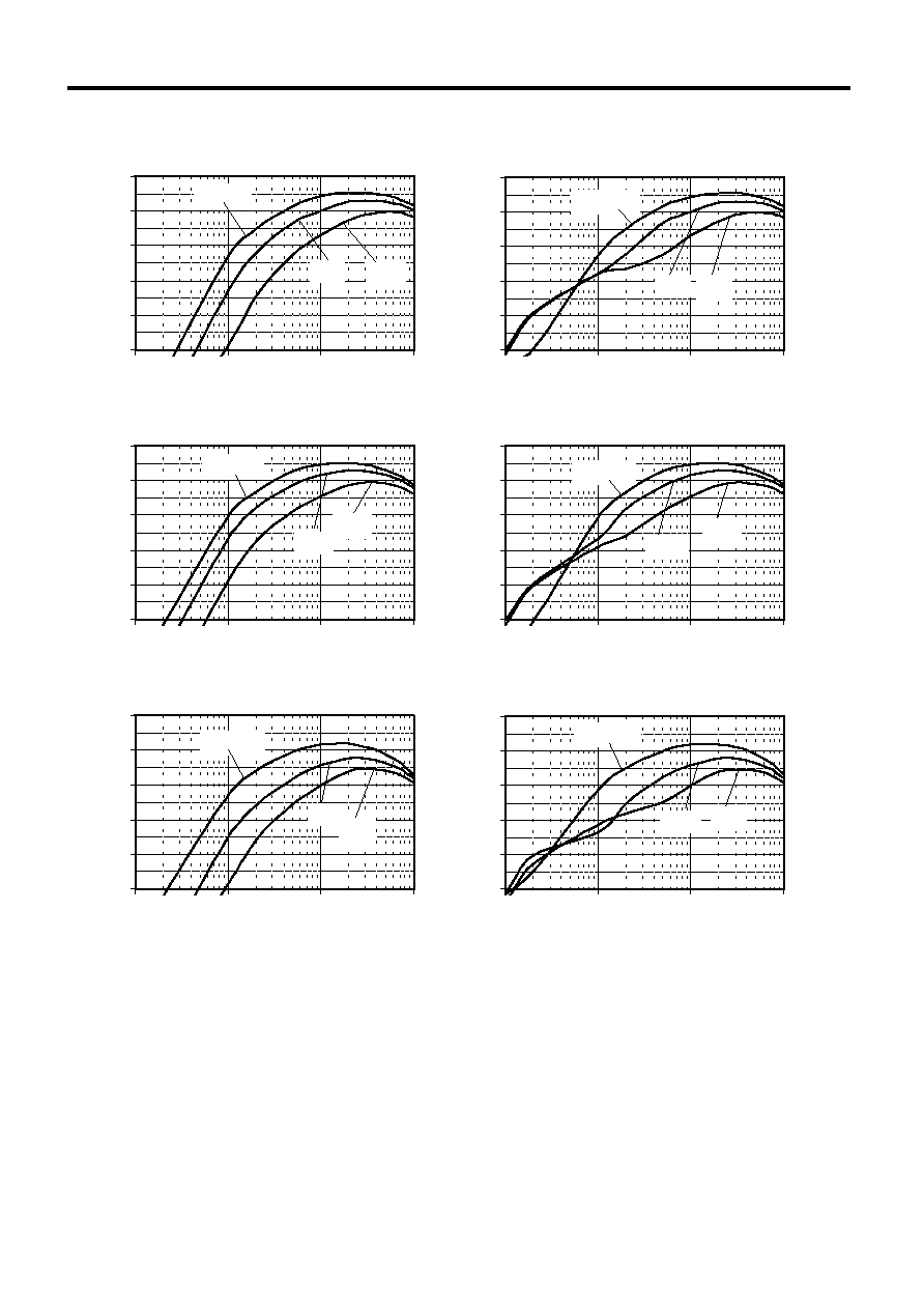
1. Efficiency
-- Output current I
OUT
Characteristics
(1) S-8540A33FN
(2) S-8541A33FN
50
60
70
80
90
100
1
10
100
1000
I
OUT
(mA)
Efficiency
(%)
V
IN
=4.0
(3.3V,600kHz,PWM control)
5.0V
7.2V
50
60
70
80
90
100
1
10
100
1000
I
OUT
(mA)
Efficiency
(%)
V
IN
=4.0V
5.0V
7.2V
(3.3V,600kHz,PWM/PFM control)
(3) S-8540A25FN
(4) S-8541A25FN
50
60
70
80
90
100
1
10
100
1000
I
OUT
(mA)
Efficiency
(%)
V
IN
=3.0V
(2.5V,600kHz,PWM control)
3.6V
5.0V
50
60
70
80
90
100
1
10
100
1000
I
OUT
(mA)
Efficiency
(%)
V
IN
=3.0V
3.6V
5.0V
(2.5V,600kHz,PWM/PFM control)
(5) S-8540A18FN
(6) S-8541A18FN
50
60
70
80
90
100
1
10
100
1000
I
OUT
(mA)
Efficiency
(%)
V
IN
=2.5V
(1.8V,600kHz,PWM control)
3.6V
5.0V
50
60
70
80
90
100
1
10
100
1000
I
OUT
(mA)
Efficiency
(%)
V
IN
=2.5V
3.6V
5.0V
(1.8V,600kHz,PWM/PFM control)
PWM Control & PWM/PFM Control High-Frequency Step-Down Switching Regulator-Controllers
Rev.1.1
_70
S-8540/8541 Series
Seiko Instruments Inc.
25
(7) S-8540C33FN
(8) S-8541C33FN
50
60
70
80
90
100
1
10
100
1000
I
OUT
(mA)
Efficiency
(%)
V
IN
=4.0
(3.3V,300kHz,PWM control)
5.0V
7.2V
50
60
70
80
90
100
1
10
100
1000
I
OUT
(mA)
Efficiency
(%)
V
IN
=4.0V
5.0V 7.2V
(3.3V,300kHz,PWM/PFM control)
(9) S-8540C25FN
(10) S-8541C25FN
50
60
70
80
90
100
1
10
100
1000
I
OUT
(mA)
Efficiency
(%)
V
IN
=3.0V
(2.5V,300kHz,PWM control)
3.6V
5.0V
50
60
70
80
90
100
1
10
100
1000
I
OUT
(mA)
Efficienvy
(%)
V
IN
=3.0V
3.6V
5.0V
(2.5V,300kHz,PWM/PFM control)
(11) S-8540C18FN
(12) S-8541C18FN
50
60
70
80
90
100
1
10
100
1000
I
OUT
(mA)
Efficiency
(%)
V
IN
=2.5V
(1.8V,300kHz,PWM control)
3.6V
5.0V
50
60
70
80
90
100
1
10
100
1000
I
OUT
(mA)
Efficiency
(%)
V
IN
=2.5V
3.6V
5.0V
(1.8V,300kHz,PWM/PFM control)

PWM Control & PWM/PFM Control High-Frequency Step-Down Switching Regulator-Controllers
S-8540/8541 Series
Rev.1.1
_70
Seiko Instruments Inc.
26
2. Ripple-- Output current I
OUT
Characteristics
(13) S-8540A33FN
(14) S-8541A33FN
0
20
40
60
80
100
1
10
100
1000
I
OUT
(mA)
Ripple(mV
)
V
IN
=4.0
(3.3V,600kHz,PWM control)
5.0V
7.2V
0
20
40
60
80
100
1
10
100
1000
I
OUT
(mA)
Ripple(mV
)
V
IN
=4.0V
5.0V
7.2V
(3.3V,600kHz,PWM/PFM control)
(15) S-8540A18FN
(16) S-8541A18FN
0
20
40
60
80
100
1
10
100
1000
I
OUT
(mA)
Ripple(mV
)
V
IN
=2.5V
(1.8V,600kHz,PWM control)
3.6V
5.0V
0
20
40
60
80
100
1
10
100
1000
I
OUT
(mA)
Ripple(mV
)
V
IN
=2.5V
3.6V
5.0V
(1.8V,600kHz,PWM/PFM control)
(17) S-8540C33FN
(18) S-8541C33FN
0
20
40
60
80
100
1
10
100
1000
I
OUT
(mA)
Ripple(mV
)
V
IN
=2.5V
(3.3V,600kHz,PWM control)
3.6V
5.0V
0
20
40
60
80
100
1
10
100
1000
I
OUT
(mA)
Ripple(mV
)
V
IN
=2.5V
3.6V
5.0V
(1.8V,300kHz,PWM/PFM control)
(19).S-8540C18FN (20).S-8541C18FN
0
20
40
60
80
100
1
10
100
1000
I
OUT
(mA)
Ripple(mV
)
V
IN
=2.5V
(1.8V,300kHz,PWM control)
3.6V
5.0V
0
20
40
60
80
100
1
10
100
1000
I
OUT
(mA)
Ripple(mV
)
V
IN
=2.5V
3.6V
5.0V
(1.8V,300kHz,PWM/PFM control)

l Reel Specifications
l Tape Specifications
l Dimensions
n 8-Pin MSOP
FN008-A
Rev.1.0
020213
2.95Ī0.2
8
5
0.2Ī0.1
0.65Ī0.1
0.13Ī0.1
1
4
No. : FN008-A-P-SD-1.0
T2(TB)
0.3Ī0.05
1.35Ī0.15
1.05Ī0.05
1.55Ī0.05
2.0Ī0.05
4.0Ī0.1
3.1Ī0.15
4.0Ī0.1
1
4
5 8
Feed direction
No. : FN008-A-C-SD-1.0
(60į)
(60į)
13Ī0.2
16.5max.
13.0Ī0.3
Winding core
No. : FN008-A-R-SD-1.0
3000 pcs/reel

∑
The information described herein is subject to change without notice.
∑
Seiko Instruments Inc. is not responsible for any problems caused by circuits or diagrams described herein
whose related industrial properties, patents, or other rights belong to third parties. The application circuit
examples explain typical applications of the products, and do not guarantee the success of any specific
mass-production design.
∑
When the products described herein are regulated products subject to the Wassenaar Arrangement or other
agreements, they may not be exported without authorization from the appropriate governmental authority.
∑
Use of the information described herein for other purposes and/or reproduction or copying without the
express permission of Seiko Instruments Inc. is strictly prohibited.
∑
The products described herein cannot be used as part of any device or equipment affecting the human
body, such as exercise equipment, medical equipment, security systems, gas equipment, or any apparatus
installed in airplanes and other vehicles, without prior written permission of Seiko Instruments Inc.
∑
Although Seiko Instruments Inc. exerts the greatest possible effort to ensure high quality and reliability, the
failure or malfunction of semiconductor products may occur. The user of these products should therefore
give thorough consideration to safety design, including redundancy, fire-prevention measures, and
malfunction prevention, to prevent any accidents, fires, or community damage that may ensue.