 | –≠–ª–µ–∫—Ç—Ä–æ–Ω–Ω—ã–π –∫–æ–º–ø–æ–Ω–µ–Ω—Ç: S-8604BWI | –°–∫–∞—á–∞—Ç—å:  PDF PDF  ZIP ZIP |

Rev.1.1
_10
Seiko Instruments Inc.
1
FOR CONTACT IMAGE SENSOR
S-8604BWI
LINEAR IMAGE SENSOR IC
The S-8604BWI is a linear image sensor suitable for a multichip
contact image sensor with resolution of 8 dots per mm. The
obtained image signals by light sensitive elements composed of
64 dots are provided sequentially as analog signals synchronous
with the clock signal.
Features
∑ Widely applicable scanning width for various sizes of paper : 8 mm.
Various sizes of paper can be read by simply changing the number of chips aligned in a line.
∑ 2-input signals : SI, CLK
Only two input signals, start and clock, can drive the IC.
∑ SIG pin reset function :
Synchronized reset with CLK signal
∑ High sensitivity :
High sensitivity photo-transistor
∑ Low image lag rate :
Image lag rate is 1 / 3 compared to the SII current products.
∑ High operation speed :
fck=2.5 MHz
∑ Low power consumption :
5 V single power supply and CMOS scanning circuit
Terminal functions
Table 1
Terminal No.
Symbol
Name
Operation
1
SI
Start input pin
Shift resister data input pin
CMOS input (Logic level is TTL-level)
2
CLK
Clock input pin
Shift register clock input pin
CMOS input (Logic level is TTL-level)
3
VDD
Power supply pin
Normally +5V
4
GND
Ground pin
Normally 0V
5
SIG
Video signal output pin
Analog image signal output pin
6
N.C.
7
SO
Start output pin
Shift register data output pin
Block diagram
SO
VDD
GND
D.G.
A.G.
SI
CLK
SIG
3
64
63
2
1
ANALOG SWITCH
∑ ∑ ∑
∑ ∑ ∑
SCANNING CIRCUIT
RESET
SCS
Figure 1

LINEAR IMAGE SENSOR IC FOR CONTACT IMAGE SENSOR
S-8604BWI
Rev.1.1
_10
2
Seiko Instruments Inc.
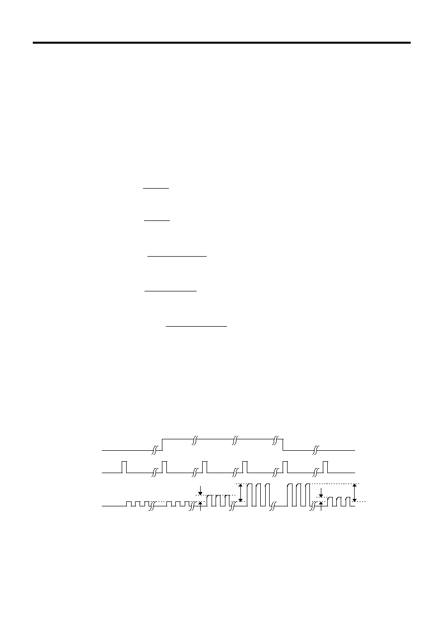
Timing chart
SO
63
62
61
60
6
5
4
3
2
1
SIG
tphl
tplh
SCS
64
CLK
th
tsu
SI
(SI for the 2nd and later ICs)
SI(SO)
Tw
1
64
62
63
61
60
6
5
4
3
2
RESET
Active high RESET signal resets the SIG signal to the GND
1
64
62
63
61
60
6
5
4
3
2
Figure 2
Absolute maximum ratings
Table 2
Parameter
Symbol
Condition
Rating
Unit
Power supply voltage
V
DD
VDD-GND
-0.4 to +7.0
V
Input voltage
V
IN
SI, CLK
-0.4 to V
DD
+0.4
V
Output voltage
V
OUT
SO, SIG
-0.4 to V
DD
+0.4
V
Operating temperature
T
opr
-5 to +85
∞C
Storage temperature
T
stg
-40 to +125
∞C
Caution The absolute maximum ratings are rated values exceeding which the product could
suffer physical damage. These values must therefore not be exceeded under
any conditions.
Electric characteristics
1) DC characteristics
Table 3
V
DD
=5V
±10%, T
OPR
=55
∞C
Rating
min.
typ.
Max.
Input voltage
V
IH
SI, CLK
2.4
V
V
IL
0.8
Input current
I
IH
SI, CLK
0.5
µA
I
IL
-0.5
Output voltage
V
OH
I
OH
= -100
µA
3.8
V
V
OL
I
OL
= 100
µA
0.4
Current consumption
I
DD
fck = 2.5 MHz
0.6
1.5
mA
Leak current
I
S
VDD-GND
0.2
µA
Unit
Condition
Symbol
Parameter
LINEAR IMAGE SENSOR IC FOR CONTACT IMAGE SENSOR
Rev.1.1
_10
S-8604BWI
Seiko Instruments Inc.
3
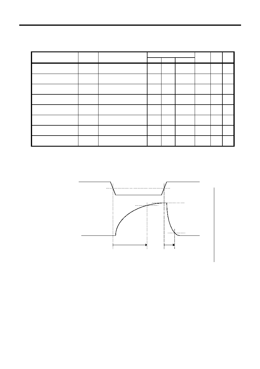
2) Switching characteristics
Table 4
V
DD
=5 V
±10 %, T
OPR
=55
∞C
Rating
A
B
min.
typ.
max.
*1)
*2)
Clock pulse width
Tw
High period of CLK
100
(1/ fck)
-100
ns
Data set up time
tsu
100
1/ fck
ns
Data hold time
th
0
(1/ fck)
-200
ns
Clock frequency
fck
Assurance of shift-
register operation
2.5
MHz
CLK-SO L-H
delay time
t
plh
fck = 2.5 MHz
C
L
= 10 pF
150
ns
CLK-SO H-L
delay time
t
phl
fck = 2.5 MHz
C
L
= 10 pF
150
ns
Output stable time 1
*3)
t
pd1
400
600
ns
Output stable time 2
*3)
t
pd2
300
ns
*1) 100% testing
*2) Sampling inspection
*3) Adopted for bright signal measurement of photoelectric conversion
characteristics.
SIG
CLK
50 %
90 %
100 %
10 %
t
pd2
t
pd1
Figure 3
Unit
Condition
Symbol
Parameter
Output Stable Time
LINEAR IMAGE SENSOR IC FOR CONTACT IMAGE SENSOR
S-8604BWI
Rev.1.1
_10
4
Seiko Instruments Inc.
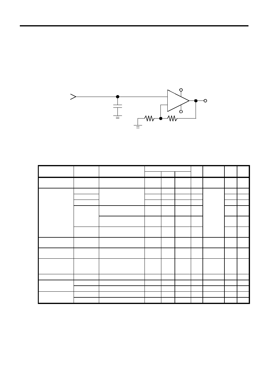
3) Photoelectric conversion characteristics
Vp is measured using the measurement circuit of Figure-4 in the following condition.
Condition : V
DD
=5 V, T
OPR
=55
∞C, fck=500 kHz (duty=50 %)
Read period RT=5 ms, Load capacitor CL=40 pF
Light source LED (
=570 nm, half width 30nm, illuminance 12 lx.)
Connecting a capacitor of 0.1
µF between VDD and GND.
+
+5V
Vp
-5V
(AD843)
SIG
40pF
-
Av=2
1k
1k
Figure 4 Measurement Circuit
Table 5
Rating
A
B
min.
typ.
max.
*1)
*2)
Bright signal
Vpave
Exposure value
Ep = 0.06lx s
0.856
1.905
V
See 3)-2
dV1
Read period
-6.0
+6.0
%
See 3)-1
Bright signal
dV2
RT = 5 ms
-6.0
+6.0
%
deviation
dV3
0.0
+7.5
%
dV4
RT = 5 ms,
i = 2 to 62
-7.0
+7.0
%
RT = 5 ms,
i = 1, 63
-15.0
+15.0
%
dV1
+dV2
RT = 5 ms,
-10.0
+10.0
%
Dark signal 1
Vd1
RT = 5 ms,
fck = 500 kHz
24
60
mV
Dark signal 2
Vd2
RT = 32 ms,
fck = 2 kHz
240
mV
Dark signal
deviation
in a wafer *4)
dark
RT = 5 ms,
fck = 500 kHz
0
9
mV
Linearity
0.95
1.1
1.2
See 3)-3
Image lag
RIL
13
%
See 3)-1
RIL_ave
10
%
See 3)-1
Light response
RIR
77
%
See 3)-1
RIR_ave
80
%
See 3)-1
*1) 100% testing
*2) Sampling inspection
*4) Deviation of the 64-bit average value of the dark signal 1 for each chip in a
wafer.
Note
Unit
Condition
Symbol
Parameter
.
.
=
LINEAR IMAGE SENSOR IC FOR CONTACT IMAGE SENSOR
Rev.1.1
_10
S-8604BWI
Seiko Instruments Inc.
5
3)-1 Parameter definition
Vp_ave : average output of all bit
Vp_max : maximum output
Vave1 : average output of the 2
nd
to 10
th
bit
Vp_min : minimum output
Vave2 : average output of the 28
th
to 36
th
bit
Vp(i): the i
th
bit output ( i =1 to 63)
Vave3 : average output of the 55
th
to 63
rd
bit
V1 = Vave2 - Vave1
V2 = Vave3 - Vave2
V1
V
p_ave
dV1 =
◊ 100 (%)
V2
V
p_ave
dV2 =
◊ 100
dV3 =
Vp_max
- Vp_min
Vp_max + Vp_min
◊ 100
dV4 =
Vp(i)
-Vp( i + 1)
Vp_ave
◊ 100
dV1
+ dV2 =
◊ 100
Vp_ave
Vave3
- Vave1
RIL : Image lag rate for the 1
st
to 64
th
bit (cf. Figure-5)
RIL_ave : Average of image lag rate for all bits (cf. Figure-5)
RIR : Light response rate for the 1
st
to 64
th
bit (cf. Figure-5)
RIR_ave : Average of light response rate for all bits (cf. Figure-5)
100%
Vp
Image lag rate : RIL
13%
Light response : RIR
77%
Vp
OFF
ON
OFF
Vd
8
7
6
2
1
LED
SIG
SI
Figure 5 Light Response Rate and Image Lag Rate
LINEAR IMAGE SENSOR IC FOR CONTACT IMAGE SENSOR
S-8604BWI
Rev.1.1
_10
6
Seiko Instruments Inc.
3)-2 Bright signal ranking
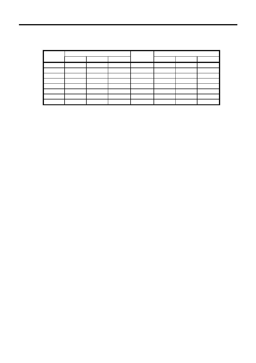
Table 6
Vp_ave (typ.)
± 2.5 %
Vp_ave(V)
Vp_ave(V)
min.(
)
typ.
max.(<)
min.(
)
typ.
max.(<)
0
0.856
0.878
0.900
8
1.277
1.309
1.342
1
0.900
0.923
0.946
9
1.342
1.377
1.411
2
0.946
0.970
0.994
A
1.411
1.447
1.483
3
0.994
1.020
1.045
B
1.483
1.521
1.559
4
1.045
1.072
1.099
C
1.559
1.599
1.639
5
1.099
1.127
1.155
D
1.639
1.681
1.723
6
1.155
1.185
1.214
E
1.723
1.768
1.812
7
1.214
1.246
1.277
F
1.812
1.858
1.905
3)-3 Linearity
The
value is calculated using the non-linear regression based on the following equation, measuring
Vp_ave every 0.01 Lx s from dark state to 0.06 Lx s.
Vp_ave = A
+ B ∑ Ep
(A,B: constant , Ep: exposure value)
RANK
RANK

LINEAR IMAGE SENSOR IC FOR CONTACT IMAGE SENSOR
Rev.1.1
_10
S-8604BWI
Seiko Instruments Inc.
7
Pad configuration
Photo detection windows
AR
7
6
5
4
AC
3
2
1
AL
Chip size : 8000
µm ◊ 350 µm (before dicing)
Pad size : 100
µm ◊ 80 µm (Opening area)
(0,0) : The coordinate origin is the center of the scribe line of the lower left corner of the IC.
The distance between the boundary of a pad opening area and peripheral Al pattern
15µm
Y
X
Figure 6
Table 7 Pad Coordinates
Unit :
µm
Coordinate
Coordinate
X
Y
X
Y
1
SI
1431
102
5
SIG
4870
102
2
CK
1832
102
6
N.C.
6223
102
3
VDD
3182
102
7
SO
7021
102
4
GND
4245
102
Table 8 Alignment Mark Coordinates
Unit:
µm
Coordinate
X
Y
AL
240
102
AC
4000
102
AR
7790
102
Chip size and sensor arrangement diagram
P
◊31
64
63
62
61
(Center of scribe line)
X
Y
145.5
32
34
33
31
80
4
3
2
1
P
79.5
P
(P=124.12)
Unit :
µm
P
P
P
P
79.5
P
◊31
8000
Chip size : 8000
µm ◊ 350 µm (Before dicing)
Shaded area : photo detection window (X=85, Y=60)
Figure 7
Note : The coordinate origin is the center of
the scribe line of the lower left corner
of the IC, and the coordinate values
point the center of the pads and the
alignment marks .
PAD No.
Name
Name
PAD No.
Alignment mark name

LINEAR IMAGE SENSOR IC FOR CONTACT IMAGE SENSOR
S-8604BWI
Rev.1.1
_10
8
Seiko Instruments Inc.
Wafer form
Note: The arrangement of IC is subject to change without notice.
Wafer thickness: 350
±
30
µ
m
Wafer diameter
:
6 inches
O
r
ient
a
t
io
n F
l
at
Wa
f
e
r N
o
.
Lot
N
o
.
(Pad side)
IC chip
(Sensor side)
Figure 8

LINEAR IMAGE SENSOR IC FOR CONTACT IMAGE SENSOR
Rev.1.1
_10
S-8604BWI
Seiko Instruments Inc.
9
Scribe line
60
(Scribe line area)
60
50
51
290
54
Unit :
µm
(Photo detection window)
(Passivasion boundary)
60
7940
Figure 9
Alignment mark
Unit :
µm
The distance between the boundary of alignment marks and
peripheral Al patterns shall be 15
µm or more.
Al pattern
Passivasion
opening
35
35
30
4
25
27.5
27.5
4
Figure 10

LINEAR IMAGE SENSOR IC FOR CONTACT IMAGE SENSOR
S-8604BWI
Rev.1.1
_10
10
Seiko Instruments Inc.
Handling precautions
Products are shipped in wafer or bare chip form. Keep these precautions when handling a product.
1. Protect against static electricity damage when mounting on a sawing or dicing machine.
∑ Wear charge-proof clothing and discharge all static electricity from body.
∑ Work on a grounded conductive mat.
∑ Ground all soldering irons and machines.
∑ Maintain room humidity from 50 to 60 %RH.
2. Prevent malfunctions due to corrosion of electrode pads.
∑ Do not store products in a high-temperature, humid and dusty environment or one that includes
corrosive gas.
∑ Coat surface of IC with silicon resin to keep surface clean.
∑ Use clear and non-static packing material.
∑ Store products in a dry box filled with dry N2 gas having the dew point ≠30∞C or less when storing
products for 3 months or more.
3. Protect the internal Al lines and protective film of the IC when mounting products.
∑ Do not damage the surface of the IC when mounting a die or bonding wires.
∑ Do not touch the surface of the IC with tweezers.
4. Maintain the stability of the IC.
∑ Always supply VDD to the IC since the substrate is n-type semiconductor.
∑ Send the null data until the Vsig signal becomes stable at power on.
∑ Coat the IC with a transparent resin like silicon resin or enclose the IC with glass.
∑ Decrease the parasitic resistance of GND line and VDD line of the circuit board on which the IC is
mounted.
∑ Decrease the parasitic capacitance between CLK and SIG of the circuit board on which the IC is
mounted.
∑ Fix the cycle and duty of the input signal while operating.
∑ Mount a capacitor between VDD and GND to prevent influence of voltage fluctuation due to the
response current of the IC. Decide the mounting method and the capacitance of the capacitor based on
evaluation of the product in an actual application.

∑
The information described herein is subject to change without notice.
∑
Seiko Instruments Inc. is not responsible for any problems caused by circuits or diagrams described herein
whose related industrial properties, patents, or other rights belong to third parties. The application circuit
examples explain typical applications of the products, and do not guarantee the success of any specific
mass-production design.
∑
When the products described herein are regulated products subject to the Wassenaar Arrangement or other
agreements, they may not be exported without authorization from the appropriate governmental authority.
∑
Use of the information described herein for other purposes and/or reproduction or copying without the
express permission of Seiko Instruments Inc. is strictly prohibited.
∑
The products described herein cannot be used as part of any device or equipment affecting the human
body, such as exercise equipment, medical equipment, security systems, gas equipment, or any apparatus
installed in airplanes and other vehicles, without prior written permission of Seiko Instruments Inc.
∑
Although Seiko Instruments Inc. exerts the greatest possible effort to ensure high quality and reliability, the
failure or malfunction of semiconductor products may occur. The user of these products should therefore
give thorough consideration to safety design, including redundancy, fire-prevention measures, and
malfunction prevention, to prevent any accidents, fires, or community damage that may ensue.