 | ÐлекÑÑоннÑй компоненÑ: S-8813 | СкаÑаÑÑ:  PDF PDF  ZIP ZIP |
S8813_E1.2_00

Rev.1.2
_00
3-CHANNEL WHITE LED DRIVER IC
(CHARGE PUMP IC WITH A BUILT-IN
CONSTANT-CURRENT CIRCUIT)
S-8813 Series
Seiko Instruments Inc.
1
The S-8813 Series is a PFM control charge pump DC-DC
converter with a built-in constant-current circuit, and was
developed using CMOS technology. Its constant current output
makes this series ideal as a power supply for current drive
LEDs.
The S-8813 Series features three output channels and can drive
three LEDs.
This series is available in two types: a variable voltage type and
a variable current setting resistance type.
Moreover, since small ceramic capacitors can be used as
external capacitors (pump capacitors, input capacitors, output
capacitors), the S-8813 Series contributes to set miniaturization.
Features
· PFM control CMOS charge pump
· Built-in constant-current circuit
· Power supply voltage: 2.7 V to 4.5 V
· Output current value: A current variable is possible between 5.0 mA and 18 mA
(At
V
IOUT1,2,3
4.0 V, V
IN
=3.0 V)
Variable voltage type and Variable current setting resistance type are available.
· Terminal output current matching: ±1% max.
· Built-in soft start circuit:
1.5 ms typ.
· Constant current output pins:
3 channels,
±5% accuracy
· Oscillation frequency:
600 kHz typ.
· ON/OFF function provided (During standby: 1 µA max.)
· Ultra-small package:
10-Pin SON(B)
Applications
· Power supply for white LED display backlights
· Constant-current circuit
· Cellular phones and PDAs using 1-cell lithium batteries
· Power supply for flat panel displays
Package
· 10-Pin SON(B) (Package drawing code: PE010-A)
Part Numbers
· S-881300CPE-IPA-TF (Variable current setting resistance type)
· S-881300BPE-IOQ-TF (Variable voltage type)
3-CHANNEL WHITE LED DRIVER IC
(CHARGE PUMP IC WITH A BUILT-IN CONSTANT-CURRENT CIRCUIT)
S-8813 Series
Rev.1.2
_00
2
Seiko Instruments Inc.
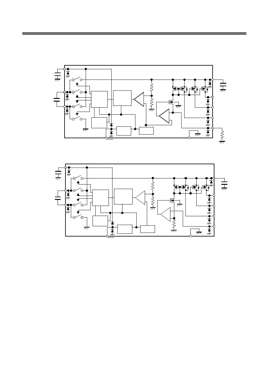
Block Diagrams
1. S-881300CPE
PFM
control
oscillator
(600 kHz)
ON/OFF
circuit
VIN
C
+
C
-
IOUT1
IOUT2
IOUT3
GND
CPOUT
RISET
Soft
Start
circuit
Switch
control
circuit
-
+
Reference
voltage
C
PUMP
=0.22
µF
C
OUT
=10
µF
R
1
*1
R
s
R
f
SW 1
SW 2
SW 3
SW 4
+
ON/OFF
C
IN
=4.7
µF
2. S-881300BPE
PFM
control
oscillator
(600 kHz)
ON/OFF
circuit
VIN
C
+
C
-
IOUT1
IOUT2
IOUT3
GND
CPOUT
VISET
Soft
Start
circuit
Switch
control
circuit
-
+
Reference
voltage
C
PUMP
=0.22
µF
C
OUT
=10
µF
R
2
*2
R
s
R
f
SW 1
SW 2
SW 3
SW 4
+
-
ON/OFF
C
IN
=4.7
µF
*1. Current setting resistance
*2. Internal resistance
Figure 1 Block Diagram
3-CHANNEL WHITE LED DRIVER IC
(CHARGE PUMP IC WITH A BUILT-IN CONSTANT-CURRENT CIRCUIT)
Rev.1.2
_00
S-8813 Series
Seiko Instruments Inc.
3
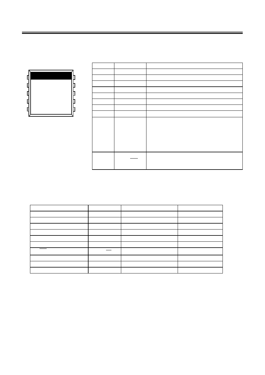
Pin Assignment
Table 1 Pin Descriptions
Pin No.
Pin Name
Function
1
IOUT1
Output pin (constant-current output)
2
IOUT2
Output pin (constant-current output)
3
IOUT3
Output pin (constant-current output)
4
C
+
Pump capacitor connection pin (positive pin)
5
C
-
Pump capacitor connection pin (negative pin)
6
GND GND
pin
7
VIN
Voltage input pin
1
2
3
4
5
10
9
8
7
6
10-Pin SON(B)
Top View
8
CPOUT
Charge pump output pin (capacitor connection pin)
Figure 2 Pin Assignment
9
RISET / VISET
Variable output current pins
In the case of RISET, a resistor is connected to this
pin and changing the resistance value can vary the
output current.
In the case of VISET, changing the voltage applied
to this pin can vary the output current.
10
OFF
ON/
Power-off pin
High level: Normal operation (Step-up operation)
Low level: Stepping-up halt (Whole circuit stopped)
Absolute Maximum Ratings
Table 2 Absolute Maximum Ratings
(Unless otherwise specified, Ta = 25
°C)
Parameter
Symbol
Absolute Maximum Rating
Unit
IOUT 1, 2, 3 pin voltage
V
IOUT1,2,3
V
SS
-0.3 to V
SS
+7 V
C
+ pin voltage
V
C+
V
SS
-0.3 to V
SS
+7.5 V
C
- pin voltage
V
C-
V
SS
-0.3 to V
SS
+7 V
VIN pin voltage
V
IN
V
SS
-0.3 to V
SS
+5 V
CPOUT pin voltage
V
CPOUT
V
SS
-0.3 to V
SS
+7 V
RISET/VISET pin voltage
V
RISET
/V
VISET
V
SS
-0.3 to V
SS
+7 V
OFF
ON/
pin voltage
OFF
ON/
V
V
SS
-0.3 to V
IN
+0.3 V
Operating temperature range
T
opr
-40 to +85
°C
Storage temperature range
T
stg
-40 to +125
°C
Power dissipation
P
D
290 mW
Caution The absolute maximum ratings are rated values exceeding which the product could suffer
physical damage. These values must therefore not be exceeded under any conditions.
3-CHANNEL WHITE LED DRIVER IC
(CHARGE PUMP IC WITH A BUILT-IN CONSTANT-CURRENT CIRCUIT)
S-8813 Series
Rev.1.2
_00
4
Seiko Instruments Inc.
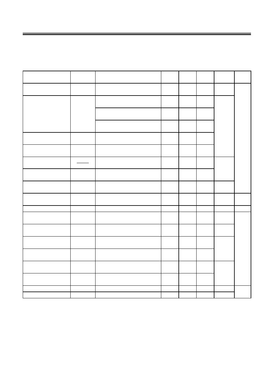
Electrical Characteristics
1. S-881300CPE
Table 3 Electrical Characteristics
(Unless otherwise specified, V
IN
= 3.0 V, current setting resistance = 5.6 k
, Ta = 25°C)
Item Symbol Conditions Min.
Typ.
Max.
Unit
Test
Circuit
Operation input
voltage
V
IN
2.7
4.5 V 2
Stabilized output current
I
OUT
V
IN
= 3.0 V to 4.5 V
V
IOUT1,2,3
*1
3.6 V
23
mA
V
IN
= 3.0 V to 4.5 V
V
I OUT1,2,3
*1
4.0 V
18
V
IN
= 2.7 V to 3.0 V
V
I OUT1,2,3
*1
3.6 V
14
Output current VI
OUT
characteristics
I
OUT1
V
IN
= 3.0 V,
V
IOUT
= 3.0 V to 4.0 V
0.5 1
Output current input
stability
I
OUT2
V
IN
= 3.0 V to 4.5 V
V
IOUT
3.6 V
0.5 1
Output current accuracy
OUT
OUT1
I
I
I
OUT1,2,3
= 17.8 mA
-5.0
+5.0 %
Inter-pin output current
variation
I
M
VI
OUT
= 3.6 V
-1.0
+1.0
Ripple voltage
V
RIP
V
IN
= 2.7 V to 4.5 V
I
OUT1,2,3
= 18 mA
100 mV
p-p
Maximum oscillation
frequency
f
osc
V
CPOUT
= 4.75 V
Measure waveform at C
- pin
540 600 660 kHz 1
Efficiency
*2
V
IN
= 3.0 V, I
OUT1,2,3
= 18 mA
82 % 2
Operation
consumption current
I
SS1
V
IN
= 2.7 V to 4.5 V
V
CPOUT
= 4.75 V
1 1.5 mA 1
Standby consumption
current
I
SSS
V
IN
= 2.7 V to 4.5 V
0.3 1 µA
Power-off pin input
voltage (high level)
V
SH
V
IN
= 2.7 V to 4.5 V
2.0
V
Power-off pin input
voltage (low level)
V
SL
V
IN
= 2.7 V to 4.5 V
0.3
Power-off pin input
current (high level)
I
SH
V
IN
= 2.7 V to 4.5 V
-0.1
0.1 µA
Power-off pin input
current (low level)
I
SL
V
IN
= 2.7 V to 4.5 V
-0.1
0.1
Soft start time
t
SS
V
IN
= 2.7 V to 4.5 V
0.3
1.5
3
ms
2
RISET pin voltage
V
RISET
V
IN
= 2.7 V to 4.5 V
0.98
1
1.02
V
*1. V
IOUT1, 2, 3
are the voltages of the IOUT pin.
*2. "Efficiency" in the electrical characteristics means the efficiency of the charge pump circuit block. The ideal
efficiency is indicated by the following expression.
Efficiency =[ V
CPOUT
× (I
OUT1
+I
OUT2
+I
OUT3
) ] / [ 2.0
× V
IN
× (I
OUT1
+I
OUT2
+I
OUT3
) ]
The ideal efficiency including the constant current circuit is expressed as following expression.
Efficiency =[ (V
IOUT1
×I
OUT1
)
+ (V
IOUT2
×I
OUT2
)
+ (V
IOUT3
×I
OUT3
) ] / [ 2.0
×V
IN
× (I
OUT1
+I
OUT2
+I
OUT3
) ]
Remark The numbers in the "test circuit" column correspond to the circuit numbers in the "Measurement
Circuits" section.
3-CHANNEL WHITE LED DRIVER IC
(CHARGE PUMP IC WITH A BUILT-IN CONSTANT-CURRENT CIRCUIT)
Rev.1.2
_00
S-8813 Series
Seiko Instruments Inc.
5
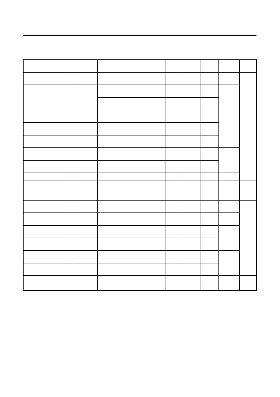
2. S-881300BPE
Table 4 Electrical Characteristics
(Unless otherwise specified, V
IN
= 3.0 V, current setting voltage = 1.8 V, Ta = 25
°C)
Item Symbol Conditions Min.
Typ.
Max.
Unit
Test
Circuit
Operation input
voltage
V
IN
2.7
4.5 V 2
Stabilized output current
I
OUT
V
IN
= 3.0 V to 4.5 V
V
IOUT1,2,3
*1
3.6 V
23
mA
V
IN
= 3.0 V to 4.5 V
V
I OUT1,2,3
*1
4.0 V
18
V
IN
= 2.7 V to 3.0 V
V
I OUT1,2,3
*1
3.6 V
14
Output current VI
OUT
characteristics
I
OUT1
V
IN
= 3.0 V,
V
IOUT
= 3.0 V to 4.0 V
0.5 1
Output current input
stability
I
OUT2
V
IN
= 3.0 V to 4.5 V
V
IOUT
3.6 V
0.5 1
Output current
accuracy
OUT
OUT1
I
I
I
OUT1,2,3
= 18 mA
-5.0
+5.0 %
Inter-pin output current
variation
I
M
V
IOUT
= 3.6 V
-1.0
+1.0
Ripple voltage
V
RIP
V
IN
=2.7 V to 4.5 V
100 mV
p-p
Maximum oscillation
frequency
f
osc
V
CPOUT
= 4.75 V
Measure waveform at C- pin
540 600 660 kHz 1
Efficiency
*2
V
IN
= 3.0 V
82 % 2
Operation
consumption current
I
SS1
V
IN
= 2.7 V to 4.5 V
V
CPOUT
= 4.75 V
1 1.5 mA 1
Standby consumption
current
I
SSS
V
IN
= 2.7 V to 4.5 V
0.3 1 µA
Power-off pin input
voltage (high level)
V
SH
V
IN
= 2.7 V to 4.5 V
2.0
V
Power-off pin input
voltage (low level)
V
SL
V
IN
= 2.7 V to 4.5 V
0.3
Power-off pin input
current (high level)
I
SH
V
IN
= 2.7 V to 4.5 V
-0.1
0.1 µA
Power-off pin input
current (low level)
I
SL
V
IN
= 2.7 V to 4.5 V
-0.1
0.1
Soft start time
t
SS
V
IN
= 2.7 V to 4.5 V
0.3
1.5
3
ms
2
VISET pin voltage
V
VISET
V
IN
= 2.7 V to 4.5 V
0.5
1.8 V
*1. V
IOUT1, 2, 3
are the voltages of the IOUT pin.
*2. "Efficiency" in the electrical characteristics means the efficiency of the charge pump circuit block. The ideal
efficiency is indicated by the following expression.
Efficiency =[ V
CPOUT
× (I
OUT1
+I
OUT2
+I
OUT3
) ] / [ 2.0
× V
IN
× (I
OUT1
+I
OUT2
+I
OUT3
) ]
The ideal efficiency including the constant current circuit is expressed as following expression.
Efficiency =[ (V
IOUT1
×I
OUT1
)
+ (V
IOUT2
×I
OUT2
)
+ (V
IOUT3
×I
OUT3
) ] / [ 2.0
×V
IN
× (I
OUT1
+I
OUT2
+I
OUT3
) ]
Remark The numbers in the "test circuit" column correspond to the circuit numbers in the "Measurement
Circuits" section.
Document Outline
- S-8813 Series
- Cover
- Features
- Applications
- Package
- Part Numbers
- Block Diagrams
- Pin Assignment
- Absolute Maximum Ratings
- Electrical Characteristics
- Measurement Circuits
- Operation
- Application Circuit Examples
- Precautions
- Major Temperature Characteristics Examples
- Major Power Supply Dependence Characteristics Examples
- Major Load Characteristics Examples
- Transient Response Characteristics Examples
- Package Drawing