 | –≠–ª–µ–∫—Ç—Ä–æ–Ω–Ω—ã–π –∫–æ–º–ø–æ–Ω–µ–Ω—Ç: S-882150A | –°–∫–∞—á–∞—Ç—å:  PDF PDF  ZIP ZIP |
Document Outline
- S-8821 Series
- Cover
- Features
- Applications
- Packages
- Block Diagram
- Selection Guide
- Pin Configurations
- Absolute Maximum Ratings
- Electrical Characteristics
- Test Circuits
- Operation
- External Capacitor Selection
- Precautions
- Typical Characteristics
- Packag drawings
- SOT-23-6W
- 6-Pin SNB(B)
- 6-Pin SON(A)

Rev.1.0
_10
VOLTAGE REGULATION
STEP-UP CHARGE PUMP DC-DC CONVERTER
S-8821 Series
Seiko Instruments Inc.
1
The S-8821 series is a CMOS step-up charge pump
DC-DC converter with a voltage regulation function.
The S-8821 series consists of an oscillation circuit, a
controller, a reference voltage circuit, an error
amplifier circuit, and an output switching transistor,
and can regulate the output voltage by PFM control.
Since small ceramic capacitors can be used for the
pump capacitor, input capacitor, and output
capacitor, the mounting area can be minimized.
Features
∑ Step-up PFM control CMOS charge pump
∑ Power supply voltage:
1.6 to 5.0 V
∑ Output voltage:
2.5 to 5.5 V, selectable in 0.1 V steps.
∑ Output voltage accuracy:
±2 % max.
∑ Built-in soft start circuit:
1.0 ms typ.
∑ Output current
25 mA (V
IN
=(V
OUT(S)
◊ 0.80) V)
∑ Oscillation frequency:
1.0 MHz typ.
∑ ON/OFF function:
During standby: 1
µA max.
∑ Ultra-small package:
SOT-23-6W, 6-Pin SNB(B), 6-Pin SON(A)
Applications
∑ Lithium ion battery driven applications
∑ Local power supply
∑ Power supply for white LED display backlights
Packages
∑ SOT-23-6W
(Package drawing code: MP006-B)
∑ 6-Pin SNB(B) (Package drawing code: BD006-A)
∑ 6-Pin SON(A) (Package drawing code: PB006-A)

VOLTAGE REGULATION STEP-UP CHARGE PUMP DC-DC CONVERTER
S-8821 Series
Rev.1.0
_10
2
Seiko Instruments Inc.
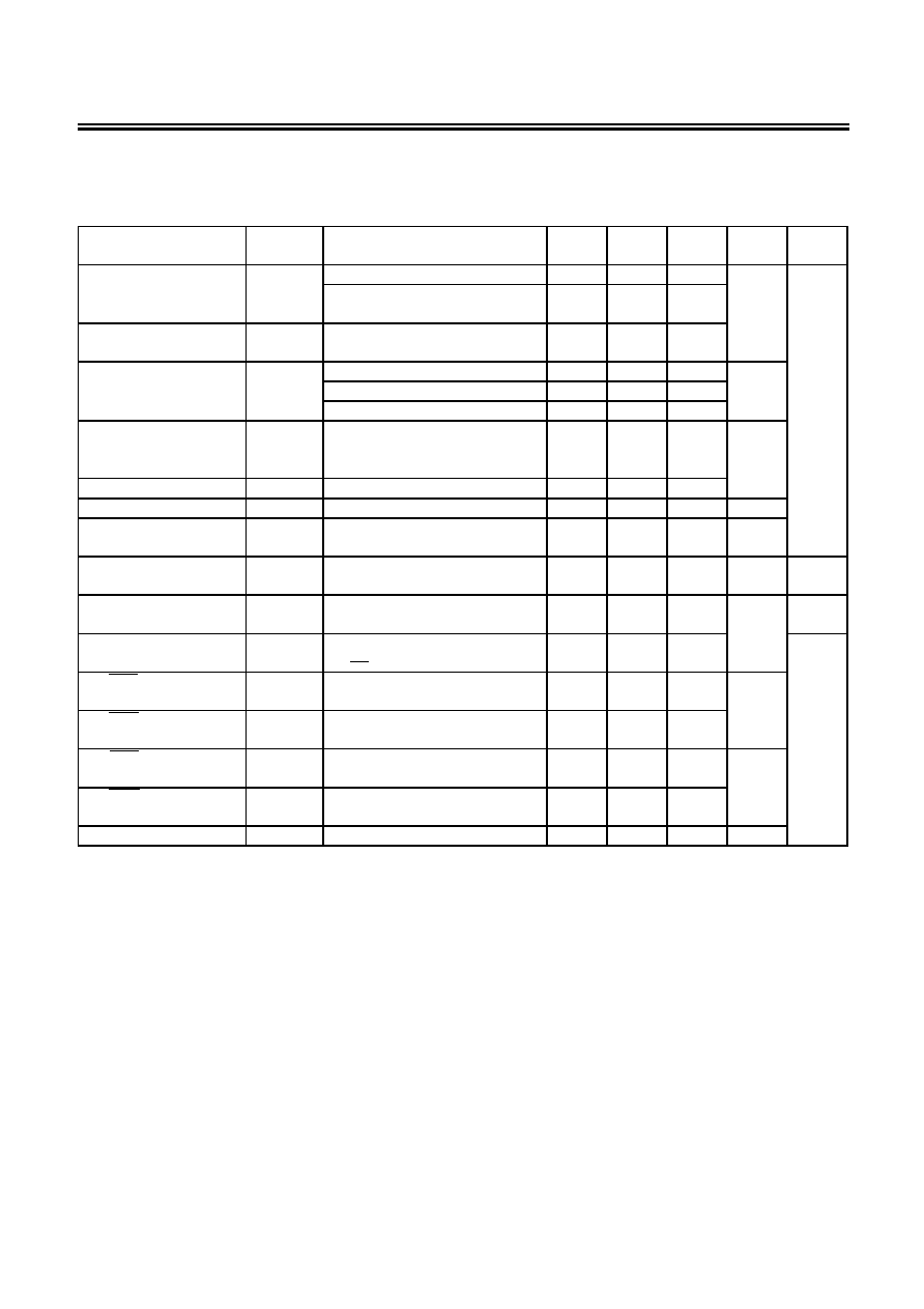
Block Diagram
VIN
Switch
control
circuit
SW1
SW2
SW3
SW4
C
+
C
-
C
PUMP
=0.10
µF
Soft start
circuit
ON/OFF
circuit
ON/OFF
PFM control
oscillator
circuit
(1.0 MHz)
Reference
voltage
+
-
VOUT
GND
C
OUT
=10
µF
R
s
R
f
C
IN
=4.7
µF
Figure 1
VOLTAGE REGULATION STEP-UP CHARGE PUMP DC-DC CONVERTER
Rev.1.0
_10
S-8821 Series
Seiko Instruments Inc.
3
Selection Guide
∑ The output voltage and packages for the S-8821 Series can be selected at the user's request. Refer to
the "Product name selection guide" for the meanings of the characters in the product name and "Product
name list" for the full product names.
1. Product name selection guide
S-8821 xx A xx ≠
xxx
≠
TF
IC direction in tape specifications
*1
Product name (abbreviation)
*2
Package name (abbreviation)
MH:
SOT-23-6W
BD: 6-Pin SNB(B)
PB: 6-Pin SON(A)
Output voltage
25 to 55
(E.g., when the output voltage is 2.5 V, it is
expressed as 25.)
*1. Refer to the taping specifications at the end of this book.
*2. Refer to the product name list.
2. Product name list
Table 1
Output Voltage
SOT-23-6W
6-Pin SNB(B)
6-Pin SON(A)
3.3 V ±2.0%
S882133AMH-M2I-TF
S882133ABD-M2I-TF
S882133APB-M2I-TF
5.0 V ±2.0%
S882150AMH-M2Z-TF
S882150ABD-M2Z-TF
S882150APB-M2Z-TF
Remark Contact the SII sales department for products with an output voltage other than those
specified above.

VOLTAGE REGULATION STEP-UP CHARGE PUMP DC-DC CONVERTER
S-8821 Series
Rev.1.0
_10
4
Seiko Instruments Inc.
Pin Configurations
Table
2
Pin No.
Symbol
Pin Description
1 VIN
Voltage
input
pin
2
C
+
Charge-pump pump capacitor connection pin (positive pin)
3
C
-
Charge-pump pump capacitor connection pin (negative pin)
4 ON/OFF
Shutdown pin
High level (H) : normal operation (step-up)
Low level (L) : step-up halt (all circuit halt)
5 GND
GND
pin
6 VOUT
Voltage
output
pin
6 4
1 3
2
SOT-23-6W
Top view
5
Figure 2
Table
3
Pin No.
Symbol
Pin Description
1 VOUT
Voltage
output
pin
2 ON/OFF
Shutdown pin
High level (H) : normal operation (step-up)
Low level (L) : step-up halt (all circuit halt)
3 GND
GND
pin
4
C
-
Charge-pump pump capacitor connection pin (negative pin)
5
C
+
Charge-pump pump capacitor connection pin (positive pin)
6 VIN
Voltage
input
pin
6-Pin SNB(B)
Top view
6
4
5
3
1
2
Figure 3
Table
4
Pin No.
Symbol
Pin Description
1 ON/OFF
Shutdown pin
High level (H) : normal operation (step-up)
Low level (L) : step-up halt (all circuit halt)
2 GND
GND
pin
3
C
-
Charge-pump pump capacitor connection pin (negative pin)
4
C
+
Charge-pump pump capacitor connection pin (positive pin)
5 VIN
Voltage
input
pin
6 VOUT
Voltage
output
pin
6-Pin SON(A)
Top view
6 5 4
1 2 3
Figure 4

VOLTAGE REGULATION STEP-UP CHARGE PUMP DC-DC CONVERTER
Rev.1.0
_10
S-8821 Series
Seiko Instruments Inc.
5
Absolute Maximum Ratings
Table 5
(Ta=25
∞C unless otherwise specified)
Items Symbols
Absolute
Maximum
Ratings
Units
C
+ pin voltage
V
C
+
V
GND
-0.3 to V
GND
+7.5
V
C
- pin voltage
V
C
-
V
GND
-0.3 to V
GND
+7
VIN pin voltage
V
IN
V
GND
-0.3 to V
GND
+5.5
VOUT pin voltage
V
OUT
V
GND
-0.3 to V
GND
+7
ON/OFF pin voltage
V
ON/OFF
V
GND
-0.3 to V
IN
+0.3
Operating temperature range
T
OPR
-40 to +85
∞C
Storage temperature range
T
STG
-40 to +125
Power dissipation
P
D1
SOT-23-6W 300
mW
P
D2
6-Pin
SON(A) 200
P
D3
6-Pin
SNB(B)
90
Caution The absolute maximum ratings are rated values exceeding which the product could suffer
physical damage. These values must therefore not be exceeded under any conditions.
VOLTAGE REGULATION STEP-UP CHARGE PUMP DC-DC CONVERTER
S-8821 Series
Rev.1.0
_10
6
Seiko Instruments Inc.
Electrical Characteristics
Table 6
(V
IN
=(V
OUT(S)
◊ 0.60) V
*1
, Ta=25
∞C unless otherwise specified)
Items Symbols Conditions
Min.
Typ.
Max.
Units
Test
circuits
Operation input voltage
V
IN
V
OUT(S)
2.9 V
1.6
5.0 V 2
V
OUT(S)
> 2.9 V
V
OUT(S)
◊
0.54
5.0
Output voltage
*2
V
OUT(E)
I
OUT
=10 mA
V
OUT(S)
◊
0.98
V
OUT(S)
V
OUT(S)
◊
1.02
Output current
*3
I
OUT
V
IN
=(V
OUT(S)
◊ 0.54) V
*6
5
mA
V
IN
=(V
OUT(S)
◊ 0.60) V
*1
15
V
IN
=(V
OUT(S)
◊ 0.80) V
25
Line regulation
V
OUT1
V
IN
=(V
OUT(S)
◊ 0.60) V
*1
to (V
OUT(S)
- 0.10) V,
I
OUT
=10 mA
50 100 mV
Load regulation
V
OUT2
I
OUT
=0.1 mA to 10 mA
40 80
Ripple voltage
*4
V
RIP
I
OUT
=10 mA
70 mV
p-p
Maximum oscillation
frequency
f
osc
V
OUT
=(V
OUT(S)
◊ 0.60) V,
Measure waveform at C
- pin
800 1000 1200 kHz
Efficiency
*5
V
IN
=(V
OUT(S)
◊ 0.54) V,
V
OUT(S)
3.0 V, I
OUT
=5 mA
90 % 1
Operation consumption
current
I
SS1
V
IN
=V
OUT(S)
,
V
OUT
=(V
OUT(S)
+ 0.5) V
35 60 µA 2
Standby consumption
current
I
SSS
V
IN
=(V
OUT(S)
◊ 0.54) V
*6
to 5.0 V,
V
ON/OFF
=0 V
0.3 1.0 1
ON/OFF pin input
voltage (high level)
V
SH
V
IN
=(V
OUT(S)
◊ 0.54) V
*6
to 5.0 V
1.5
V
ON/OFF pin input
voltage (low level)
V
SL
V
IN
=(V
OUT(S)
◊ 0.54) V
*6
to 5.0 V
0.3
ON/OFF pin input
current (high level)
I
SH
V
IN
=(V
OUT(S)
◊ 0.54) V
*6
to 5.0 V
-0.1
0.1 µA
ON/OFF pin input
current (low level)
I
SL
V
IN
=(V
OUT(S)
◊ 0.54) V
*6
to 5.0 V
-0.1
0.1
Soft start time
t
SS
I
OUT
=10 mA
0.2
1.0
4.0
ms
*1. In case of V
OUT
3.3 V, V
IN
=2.0 V
*2. V
OUT(E)
: Actual output voltage
V
OUT(S)
: Specified output voltage
*3. The output current at which the output voltage becomes 97 % of V
OUT(E)
after gradually increasing the
output current.
*4. Design
assurance
*5. The ideal efficiency is indicated by the following expression.
Efficiency
(
)=(V
OUT
◊ I
OUT
) / (2.0
◊ V
IN
◊ I
OUT
)
*6. In case of V
OUT
2.9 V, V
IN
=1.6 V
VOLTAGE REGULATION STEP-UP CHARGE PUMP DC-DC CONVERTER
Rev.1.0
_10
S-8821 Series
Seiko Instruments Inc.
7
Test Circuits
1.
VOUT
GND
ON/OFF
C
-
C
+
VIN
A
A
A
A
A
4.7
µF
Figure
5
2.
VOUT
GND
ON/OFF
C
-
C
+
VIN
A
A
4.7
µF
0.1
µF
10
µF
Figure
6

VOLTAGE REGULATION STEP-UP CHARGE PUMP DC-DC CONVERTER
S-8821 Series
Rev.1.0
_10
8
Seiko Instruments Inc.
Operation
1. Basic operation
Figure 7 shows the block diagram of the S-8821 Series.
The S-8821 series controls the output voltage by using the pulse frequency modulation (PFM) method.
The SW1 to SW4 switching transistors are switched ON/OFF with the clock generated by the internal
oscillator circuit, and operates the step-up charge pump.
The output voltage is fed back and the voltage split by feedback resistances R
s
and R
f
and reference
voltage (V
ref
) are compared by a comparator. This comparator signal is used to modulate the oscillation
pulse frequency in order to keep the output voltage constant.
VIN
Switch
control
circuit
SW1
SW2
SW3
SW4
C
+
C
-
C
PUMP
=0.10
µF
Soft start
circuit
ON/OFF
circuit
ON/OFF
PFM control
oscillator
circuit
(1.0 MHz)
Reference
voltage
+
-
VOUT
GND
C
OUT
=10
µF
R
s
R
f
C
IN
=4.7
µF
Figure 7
VOLTAGE REGULATION STEP-UP CHARGE PUMP DC-DC CONVERTER
Rev.1.0
_10
S-8821 Series
Seiko Instruments Inc.
9
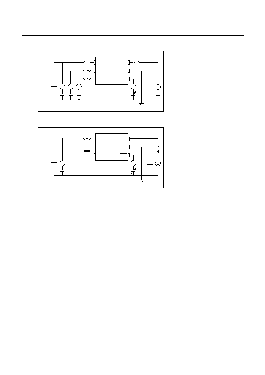
2. Step-up Charge Pump
The step-up charge pump steps up the voltage by switching ON/OFF of the SW1 to SW4 switching
transistors.
First, in order to charge the pump capacitance (C
PUMP
), set SW1 to OFF, SW2 to ON, SW3 to OFF, and
SW4 to ON (charge cycle). Following charging the electricity, in order to discharge the charged
electricity to the output capacitance (C
OUT
), SW1 set the switches as to ON, SW2 to OFF, SW3 to ON,
and SW4 to OFF (discharge cycle).
The input voltage can be stepped up to a constant voltage value by repeating this charge cycle and
discharge cycle.
Figure 8 shows the charge cycle, and figure 9 shows the discharge cycle.
V
IN
SW 1: OFF
SW 3: OFF
SW 4: ON
SW 2: ON
C
OUT
10
µF
C
PUMP
0.10
µF
Current flow
Figure 8
V
IN
SW 1: ON
SW 3: ON
SW 4: OFF
SW 2: OFF
C
OUT
10
µF
C
PUMP
0.10
µF
Current flow
Figure 9
VOLTAGE REGULATION STEP-UP CHARGE PUMP DC-DC CONVERTER
S-8821 Series
Rev.1.0
_10
10
Seiko Instruments Inc.
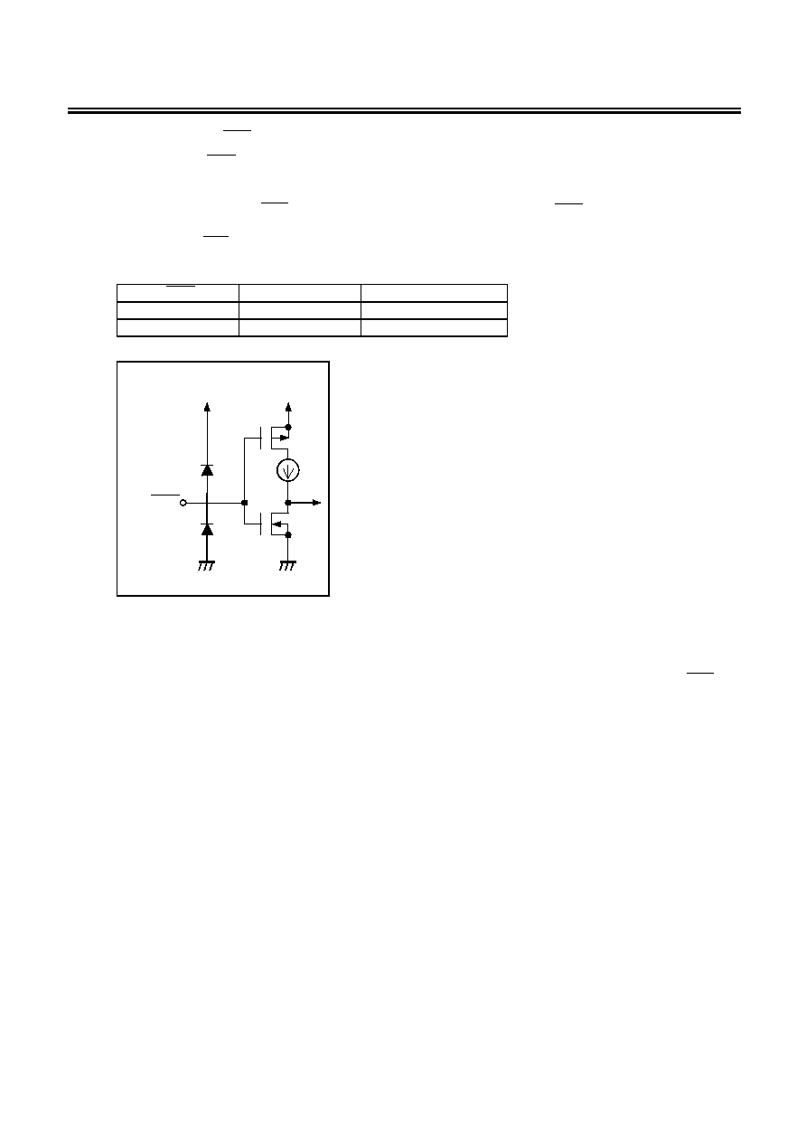
3. Shutdown Pin (ON/OFF Pin)
Setting the ON/OFF pin to the Low level ("L") causes the voltage of the VOUT pin to change to the GND
level and simultaneously the operation of all the internal circuit to stop. At this time, the consumption
current is largely reduced, to a level of approximately 0.3
µA.
The structure of the ON/OFF pin is as shown in Figure 10. Since the ON/OFF pin is neither pulled
down nor pulled up internally, do not use it in the floating state.
When the ON/OFF pin is not used, connect it to the VIN pin.
Table 7
ON/OFF pin
Internal circuit
VOUT pin voltage
"H": Power on
Operating
Set value
"L": Power off
Stop
V
GND
level
GND
ON/OFF
VIN
VIN
Figure 10
4. Soft Start Function
The S-8821 Series features a built-in soft start circuit. Upon power application or when the
OFF
ON/
pin
is switched from "L" to "H", the output voltage gradually rises over the soft start time, and the output
current is gradually output as a result. This soft start function reduces the input current rush.

VOLTAGE REGULATION STEP-UP CHARGE PUMP DC-DC CONVERTER
Rev.1.0
_10
S-8821 Series
Seiko Instruments Inc.
11
External Capacitor Selection
1. Input and Output Capacitors (C
IN
, C
OUT
)
The input capacitor (C
IN
) lowers the power supply impedance and averages the input current.
The C
IN
value is selected according to the impedance of the power supply that is used. Select a
ceramic capacitor with a small equivalent series resistance (ESR). Although this figure varies according
to the impedance of the power supply that is used as well as the load current value, it is generally in the
range of 4.7
µF to 10 µF.
For the output capacitor (C
OUT
), select a ceramic capacitor with a small ESR for smoothing the ripple
voltage. A value of 10
µF is recommended for the capacitance value. Use of a capacitor with a
capacitance lower than 10
µF results in a larger ripple voltage. Conversely, use of a capacitor with a
capacitance greater than 10
µF results in the output voltage not being able to rise up to setting value
and the impossibility to obtain the desired output current.
2. Pump Capacitor (C
PUMP
)
The pump capacitor (C
PUMP
) is required for stepping up the voltage. Select a ceramic capacitor with a
small ESR. A capacitance value of 0.10
µF is recommended. Use of a capacitor with a capacitance
greater than 0.10
µF results in a larger ripple voltage. Conversely, use of a capacitor with a
capacitance lower than 0.10
µF results in the output voltage not being able to raise up to setting value
and the impossibility to obtain the desired output current.

VOLTAGE REGULATION STEP-UP CHARGE PUMP DC-DC CONVERTER
S-8821 Series
Rev.1.0
_10
12
Seiko Instruments Inc.
Precautions
∑ Regarding the wiring to the VIN pin, VOUT pin, C+ pin, C- pin and GND pin, be careful to perform
pattern wiring so as to obtain low impedance.
∑ Always connect a capacitor to the VOUT pin, C+ pin, and C- pin.
∑ Connect C
IN
and C
OUT
in the vicinity of the IC and sufficiently strengthen the wiring for GND pin and VIN
pin in order to lower the impedance of the wiring resistance, etc. High impedance may cause unstable
operation.
Moreover, in selecting C
IN
and C
OUT
, perform a full evaluation of the actual usage conditions.
∑ Connect C
PUMP
in the vicinity of the IC and sufficiently strengthen the wiring for the C
+ pin and C- pin in
order to lower the impedance of the wiring resistance, etc. High impedance may cause instable
operation.
Moreover, in selecting C
PUMP
, perform a full evaluation of the actual usage conditions.
∑ The ON/OFF pin is configured as shown in Figure 10 and is neither pulled up or down internally, so do
not use this pin in a floating state. When not using the ON/OFF pin, connect it to the VIN pin.
Moreover, please do not apply voltage higher than VIN
+ 0.3 V to an ON/OFF pin. Current flows for a
VIN pin through the protection diode inside IC.
∑ Since this IC consists of double step-up circuits, it cannot set more than twice voltage of V
IN
to V
OUT(S)
.
∑ Be careful about the usage conditions for the input/output voltages and output current to make sure that
dissipation within the IC does not exceed the allowable power dissipation of the package.
For reference, the calculation of the power consumption in this IC is shown below.
P
D
=(V
IN
◊ 2.0 - V
OUT
)
◊ (I
OUT
)
Reference: V
IN
=4.2 V, V
OUT
=5.5 V, I
OUT
=10 mA
P
D
=(4.2
◊ 2.0 - 5.5) ◊ 0.010=29 mW
0
50
100
150
600
6-Pin SON(A)
Po
we
r
di
ssip
a
t
i
on
P
D
[m
W]
6-Pin SNB(B)
SOT-23-6W
Ambient temperature Ta [
∞C
]
Not mounted
400
200
0
Figure 11
∑ Since the information described herein is subject to change without notice, confirm that this is the latest
one before using.
∑ Do not apply an electrostatic discharge to this IC that exceeds the performance ratings of the built-in
electrostatic protection circuit.
∑ SII claims no responsibility for any and all disputes arising out of or in connection with any infringement
of the products including this IC upon patents owned by a third party.
VOLTAGE REGULATION STEP-UP CHARGE PUMP DC-DC CONVERTER
Rev.1.0
_10
S-8821 Series
Seiko Instruments Inc.
13
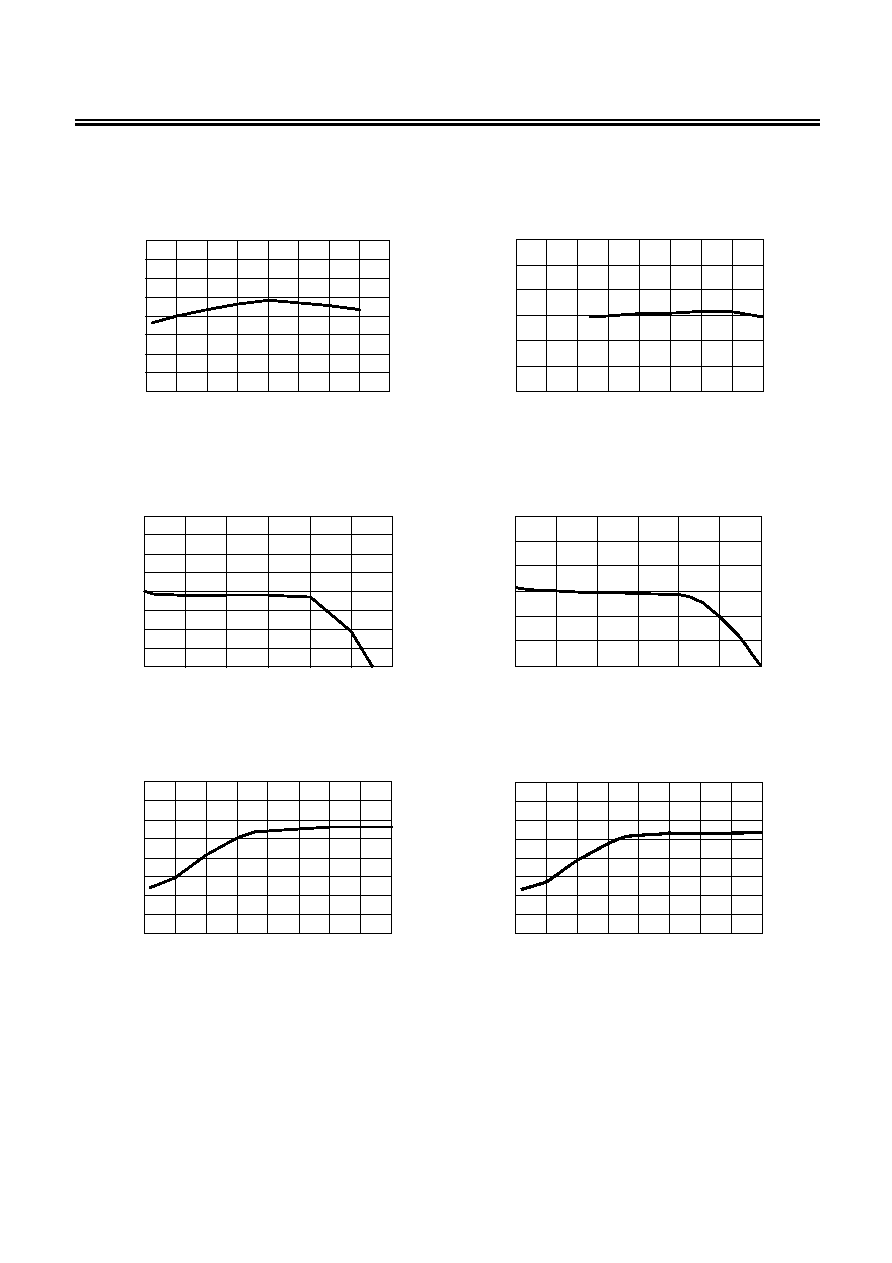
Typical Characteristics
(1) Output voltage vs. Operation input voltage
S-882133A S-882150A
I
OUT
=10 mA, Ta=25∞C
I
OUT
=10 mA, Ta=25∞C
V
OU
T
[V
]
1.5
2.0
2.5
3.0
3.5
5.5
3.15
3.10
3.50
3.20
3.25
3.35
3.30
3.40
3.45
4.0
4.5
5.0
V
OU
T
[V
]
1.5
2.5
3.0
3.5
5.5
4.80
4.70
5.30
5.20
5.10
5.00
4.90
2.0
4.0
4.5
5.0
V
IN
[V]
V
IN
[V]
(2) Output voltage vs. Output current
S-882133A S-882150A
V
IN
=2.0 V, Ta=25∞C
V
IN
=3.0 V, Ta=25∞C
V
OU
T
[V
]
0
5
10
20
30
3.15
3.10
3.50
3.40
3.35
3.30
3.25
3.20
25
15
3.45
V
OU
T
[V
]
0
10
15
20
30
4.70
5.30
5.20
5.10
5.00
4.90
4.80
5
25
I
OUT
[mA]
I
OUT
[mA]
(3) Operation consumption vs. Operation input voltage
S-882133A S-882150A
Ta=25∞C
Ta=25∞C
I
SS1
[
µ
A]
1.5
3.5
4.0
5.5
15
10
50
40
35
30
25
20
5.0
4.5
45
2.0
2.5
3.0
I
SS1
[
µ
A]
1.5
2.5
5.5
10
50
35
30
20
3.5
40
25
45
15
3.0
4.0
2.0
4.5
5.0
V
IN
[V]
V
IN
[V]
VOLTAGE REGULATION STEP-UP CHARGE PUMP DC-DC CONVERTER
S-8821 Series
Rev.1.0
_10
14
Seiko Instruments Inc.
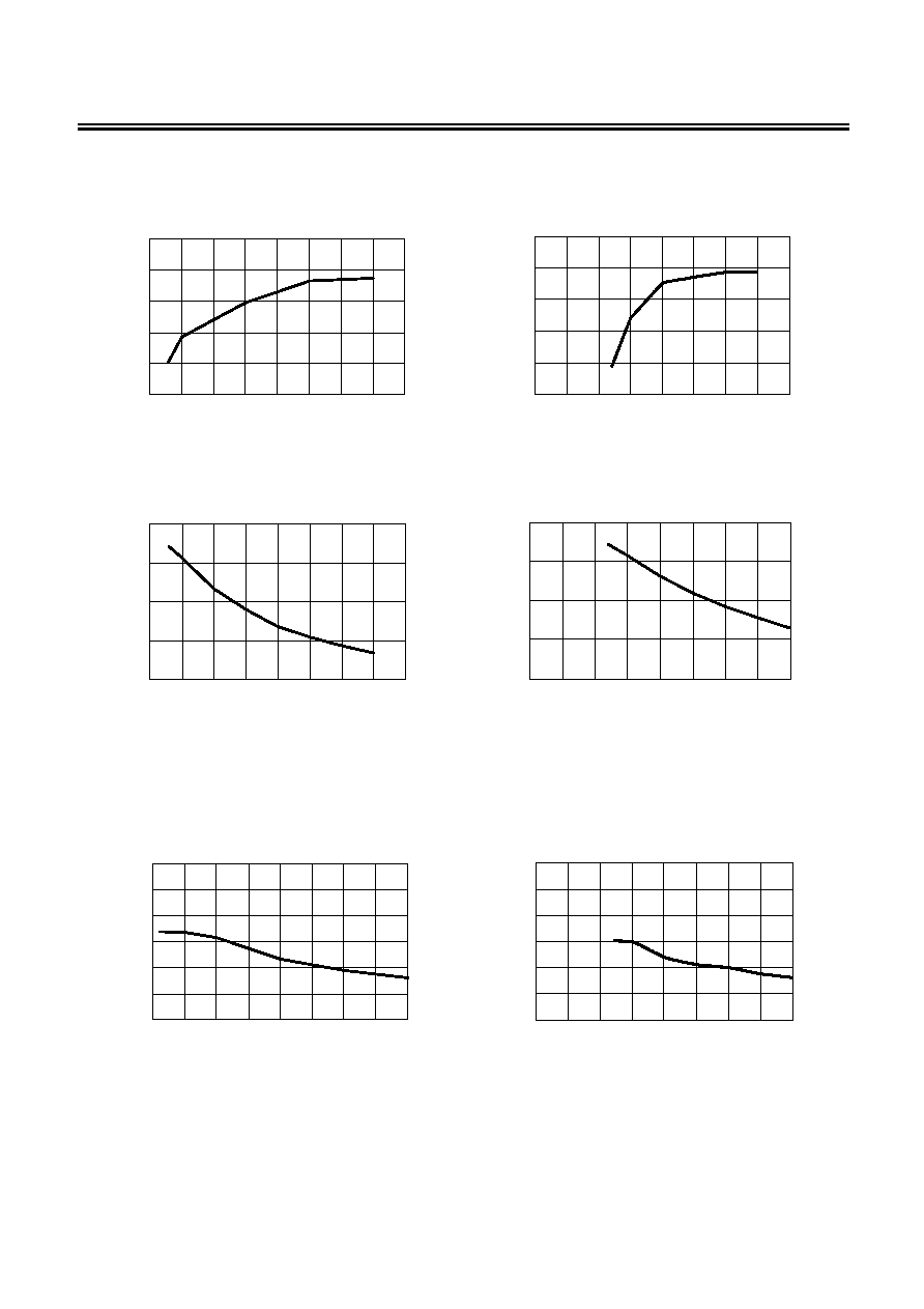
(4) Ripple voltage vs. Operation input voltage
S-882133A S-882150A
I
OUT
=10 mA, Ta=25∞C
I
OUT
=10 mA, Ta=25∞C
V
RI
P
[m
V
p-
p
]
1.5
3.0
3.5
4.0
5.0
5.5
0
20
40
60
100
4.5
2.0
2.5
80
V
RI
P
[m
V
p-
p
]
1.5
2.5
3.0
3.5
5.0
5.5
20
0
40
60
100
4.5
80
4.0
2.0
V
IN
[V]
V
IN
[V]
(5) Efficiency
*1
vs. Operation input voltage
S-882133A S-882150A
I
OUT
=10 mA, Ta=25∞C
I
OUT
=10 mA, Ta=25∞C
[%
]
1.5
2.0
3.5
4.5
5.5
20
40
60
80
100
4.0
5.0
3.0
2.5
[%
]
1.5
2.5
3.5
5.5
20
40
60
80
100
4.0
3.0
4.5
5.0
2.0
V
IN
[V]
V
IN
[V]
*1. The ideal efficiency is indicated by the following expression.
Efficiency
(
)=(V
OUT
◊ I
OUT
) / (2.0
◊ V
IN
◊ I
OUT
)
(6) Maximum oscillation frequency vs. Operation input voltage
S-882133A S-882150A
Ta=25∞C
Ta=25∞C
f
OS
C
[k
Hz]
1.5
2.0
2.5
3.5
5.0
5.5
700
800
900
1000
1100
1200
1300
4.0
4.5
3.0
f
OS
C
[k
Hz]
1.5
2.0
2.5
4.0
5.0
5.5
700
800
900
1000
1100
1200
1300
4.5
3.5
3.0
V
IN
[V]
V
IN
[V]

VOLTAGE REGULATION STEP-UP CHARGE PUMP DC-DC CONVERTER
Rev.1.0
_10
S-8821 Series
Seiko Instruments Inc.
15
(7) Load fluctuation
S-882133A S-882150A
V
IN
=2.0 V
V
IN
=3.0 V
CH1
CH2
1 mA
10 mA
CH1
CH2
1 mA
10 mA
[1 ms/div.]
[1 ms/div.]
CH1: V
OUT
[20 mV/div.]
CH2: I
OUT
[2 mA/div.]
CH1: V
OUT
[20 mV/div.]
CH2: I
OUT
[2 mA/div.]
(8) Input voltage fluctuation
S-882133A S-882150A
I
OUT
=10 mA
I
OUT
=10 mA
CH1
CH2
1.8 V
3.3 V
CH1
CH2
3.0 V
5.0 V
[1 ms/div.]
[1 ms/div.]
CH1:
V
OUT
[20 mV/div.]
CH2: V
IN
[1 V/div.]
CH1: V
OUT
[20 mV/div.]
CH2: V
IN
[1 V/div.]
2.9±0.2
0.15
1.9±0.2
1
2
3
4
6
5
0.4
0.95
+0.1
-0.08
0.95
+0.1
-0.05
No. MP006-B-P-SD-1.0
SOT236-B-PKG Dimensions
MP006-B-P-SD-1.0
Seiko Instruments Inc.
No. MP006-B-C-SD-1.0
SOT236-B-Carrier Tape
MP006-B-C-SD-1.0
Seiko Instruments Inc.
1
2
3
4 5 6
¯1.5
+0.1
-0
2.0±0.05
¯1.0
+0.2
-0
4.0±0.1
1.4±0.2
0.25±0.1
3.2±0.2
Feed direction
4.0±0.1(10 pitches:40.0±0.2)
12.5max.
9.0±0.3
¯13±0.2
(60∞)
(60∞)
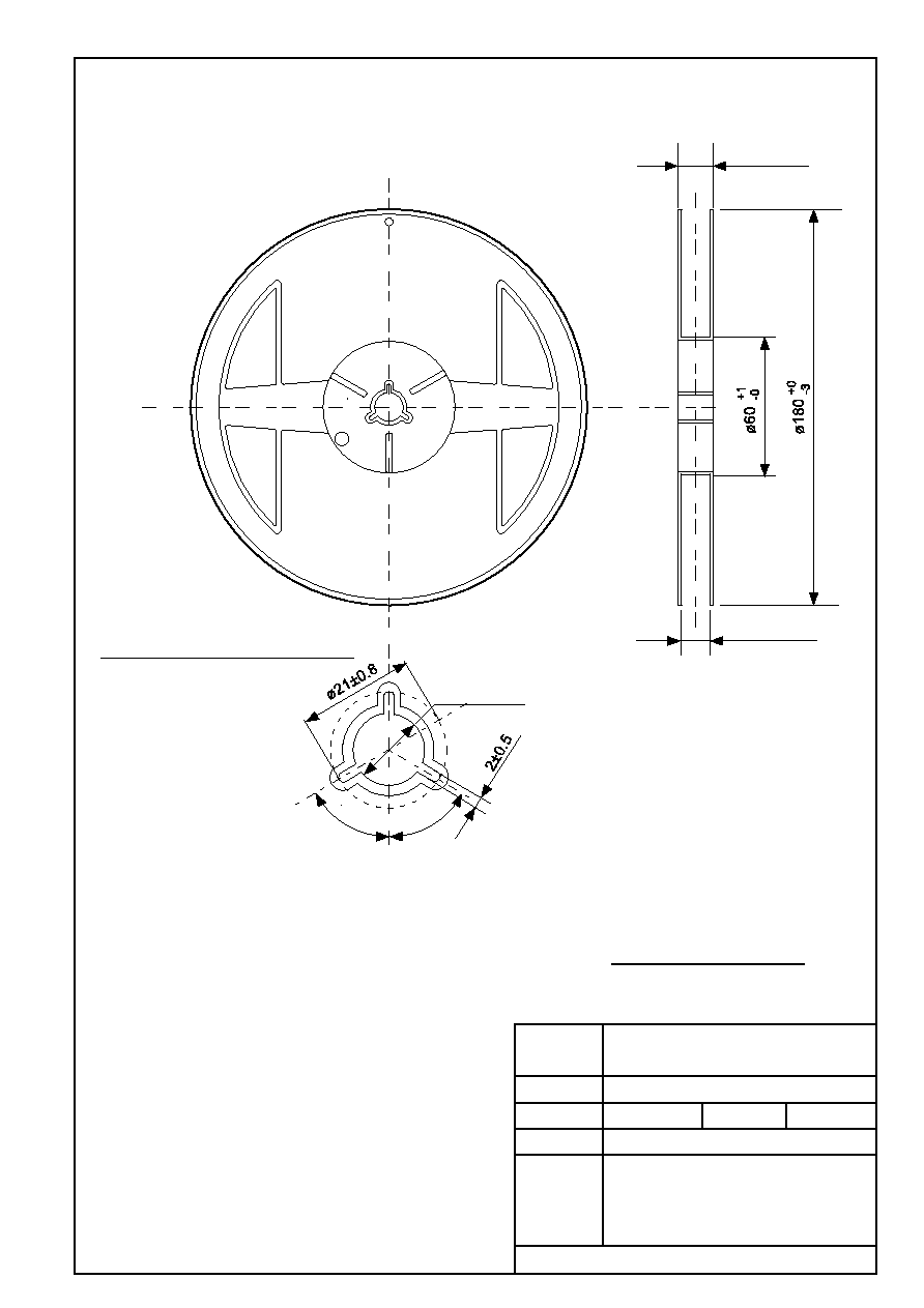
SOT236-B-Reel
MP006-B-R-SD-1.0
Seiko Instruments Inc.
No. MP006-B-R-SD-1.0
Enlarged drawing in the central part

1.8±0.15
0.5±0.1
0.5±0.1
0.8±0.05
0.14±0.05
R(0.075)
0.2±0.08
(0.125)
1
2
3
4
5
6
SNB6B-A-PKG Dimensions
No. BD006-A-P-SD-1.1
Seiko Instruments Inc.
No.
TITLE
SCALE
UNIT
mm
BD006-A-P-SD-1.1

No.
TITLE
SCALE
UNIT
mm
4.0±0.1
2.0±0.05
4.0±0.1
¯1.5±0.1
2.2±0.1
1.1±0.1
0.25±0.05
¯1.1±0.1
Seiko Instruments Inc.
Feed direction
SNB6B-A-Carrier Tape
No. BD006-A-C-SD-2.1
BD006-A-C-SD-2.1
1
2
3
6
5
4
QTY.
3,000
No.
TITLE
SCALE
UNIT
mm
12.5max.
9.0±0.3
¯13±0.2
Seiko Instruments Inc.
Enlarged drawing in the central part
SNB6B-A-Reel
No. BD006-A-R-SD-1.1
BD006-A-R-SD-1.1
No.
TITLE
SCALE
UNIT
mm
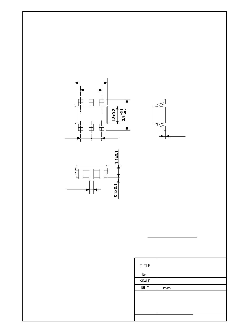
No. PB006-A-P-SD-1.0
PB006-A-P-SD-1.0
SON6A-A-PKG Dimensions
Seiko Instruments Inc.
1.6±0.2
6
4
0.3typ.
1
3
0.2
0.5
+0.1
-0.05

¯1.05±0.05
0.2±0.05
1.1±0.1
¯1.55±0.05
2.0±0.05
4.0±0.1
1.9±0.1
4.0±0.1
No.
TITLE
SCALE
UNIT
mm
1
3
4
6
No. PB006-A-C-SD-1.0
PB006-A-C-SD-1.0
SON6A-A-Carrier Tape
Feed direction
Seiko Instruments Inc.
No.
TITLE
SCALE
UNIT
mm
QTY.
3000
No. PB006-A-R-SD-1.0
PB006-A-R-SD-1.0
SON6A-A-Reel
Seiko Instruments Inc.
12.5max.
9.0±0.3
¯13±0.2
(60∞)
(60∞)
Enlarged drawing in the central part

∑
The information described herein is subject to change without notice.
∑
Seiko Instruments Inc. is not responsible for any problems caused by circuits or diagrams described herein
whose related industrial properties, patents, or other rights belong to third parties. The application circuit
examples explain typical applications of the products, and do not guarantee the success of any specific
mass-production design.
∑
When the products described herein are regulated products subject to the Wassenaar Arrangement or other
agreements, they may not be exported without authorization from the appropriate governmental authority.
∑
Use of the information described herein for other purposes and/or reproduction or copying without the
express permission of Seiko Instruments Inc. is strictly prohibited.
∑
The products described herein cannot be used as part of any device or equipment affecting the human
body, such as exercise equipment, medical equipment, security systems, gas equipment, or any apparatus
installed in airplanes and other vehicles, without prior written permission of Seiko Instruments Inc.
∑
Although Seiko Instruments Inc. exerts the greatest possible effort to ensure high quality and reliability, the
failure or malfunction of semiconductor products may occur. The user of these products should therefore
give thorough consideration to safety design, including redundancy, fire-prevention measures, and
malfunction prevention, to prevent any accidents, fires, or community damage that may ensue.