 | ÐлекÑÑоннÑй компоненÑ: S-89120A | СкаÑаÑÑ:  PDF PDF  ZIP ZIP |
Rev.1.2
_10
MINI ANALOG SERIES
CMOS SINGLE OPERATIONAL AMPLIFIER
S-891xxA Series
Seiko Instruments Inc.
1
The mini-analog series is a group of ICs that incorporate a general
purpose analog circuit in an ultra-small package.
The S-891xxA Series is a CMOS type single operational amplifier
that has a phase compensation circuit, and that can be driven at a
lower voltage with lower current consumption than existing bipolar
operational amplifiers. These features make this product the ideal
solution for small battery-powered portable equipment.
Features
Application
CMOS operational amplifier
Cellular phones
Low operating voltage:
V
DD
= 1.8 to 5.5 V
Cameras
Low current consumption: I
DD
= 50 µA (S-89110ANC)
PDAs
I
DD
= 10 µA (S-89120ANC)
Notebook PCs
Low input offset voltage (4.0 mV max.)
Digital cameras
No external capaciters required for internal phase compensation
Digital video cameras
Output full swing
Small package (SC-88A: 2.0 mm
× 2.1 mm)
Package
SC-88A (PKG drawing code: NP005-B)
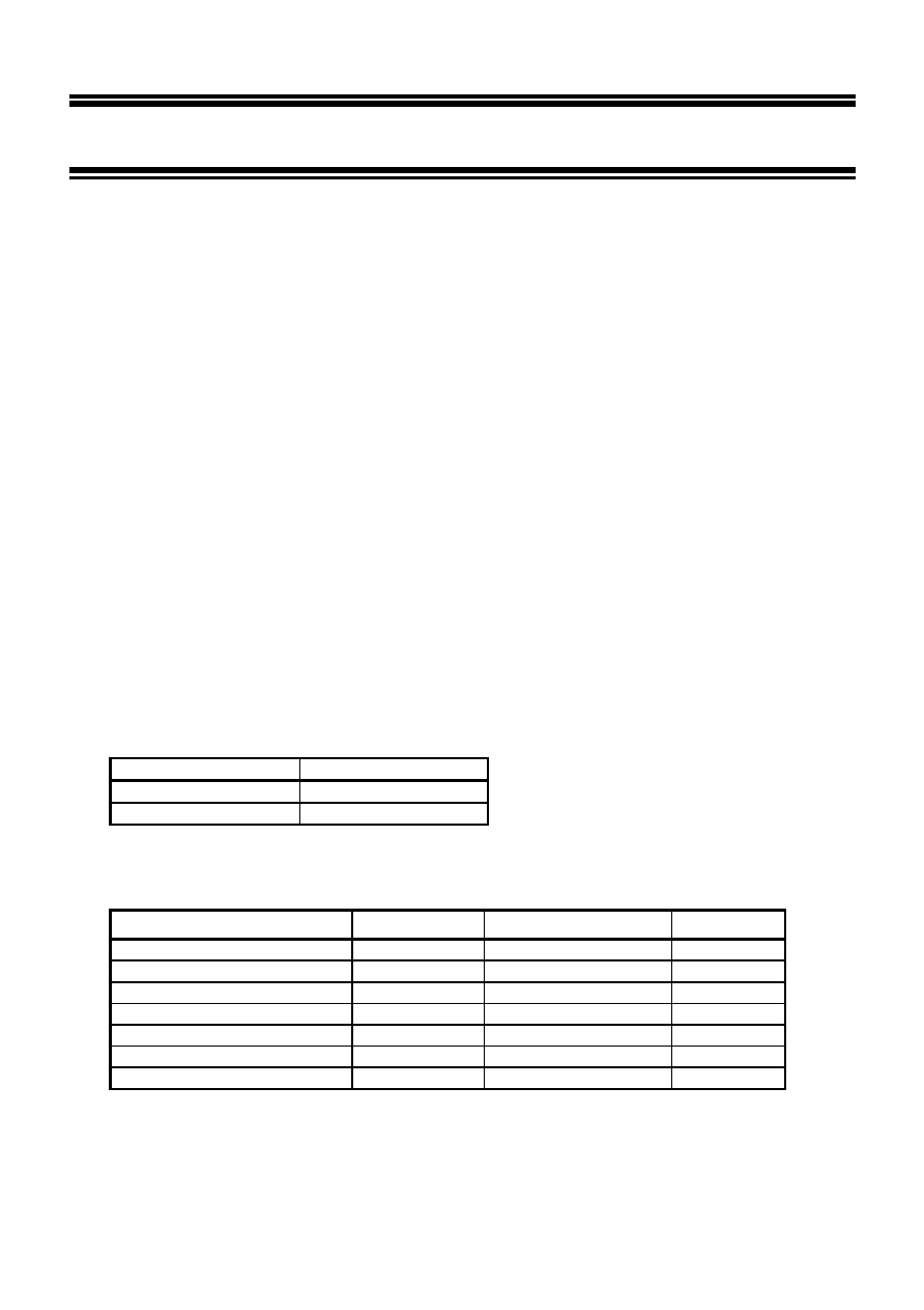
Selection Guide
Table 1
Current consumption
Product Name
I
DD
= 50 µA
S-89110ANC-1A1-TF
I
DD
= 10 µA
S-89120ANC-1A2-TF
Absolute Maximum Ratings
Table 2
Parameter
Symbol
Ratings
Unit
Power supply voltage
V
DD
- V
SS
10.0
V
Input voltage
V
IN
V
SS
to V
DD
(7.0 max.)
V
Output voltage
V
OUT
V
SS
to V
DD
(7.0 max.)
V
Differential input voltage
V
IND
±7.0
V
Power dissipation
P
D
200
mW
Operating temperature range
T
opr
-40 to +85
°C
Storage temperature range
T
stg
-55 to +125
°C
Caution The absolute maximum ratings are rated values exceeding which the product could
suffer physical damage. These values must therefore not be exceeded under any
conditions.
CMOS SINGLE OPERATIONAL AMPLIFIER
Rev. 1.2
_10
S-891xxA Series
2
Seiko Instruments Inc.
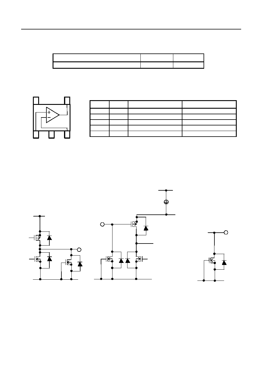
Recommended Operating Power Supply Voltage Range
Table 3
Parameter
Symbol
Range
Operating power supply voltage range
V
DD
1.8 to 5.5 V
Pin Configuration
Table 4
Figure 1
[Internal equivalent circuits]
<1> Output pin
<2> Input pin
<3> VDD pin
VDD
VSS
VSS
VDD
VSS
VDD
Figure 2
Figure 3
Figure 4
(S-89110ANC, S-89120ANC)
5-Pin SC-88A Top View
VSS
IN(
+)
IN(
-)
VDD
OUT
1
2
3
5
4
Pin No. Symbol
Description
Internal Equivalent Circuit
1
IN(
+) Non-inverted input pin
Figure 3
2
VSS
GND pin
3
IN(
-) Inverted input pin
Figure 3
4
OUT
Output pin
Figure 2
5
VDD
Positive power supply pin
Figure 4
Rev.1.2
_10
CMOS SINGLE OPERATIONAL AMPLIFIER
S-891xxA Series
Seiko Instruments Inc.
3
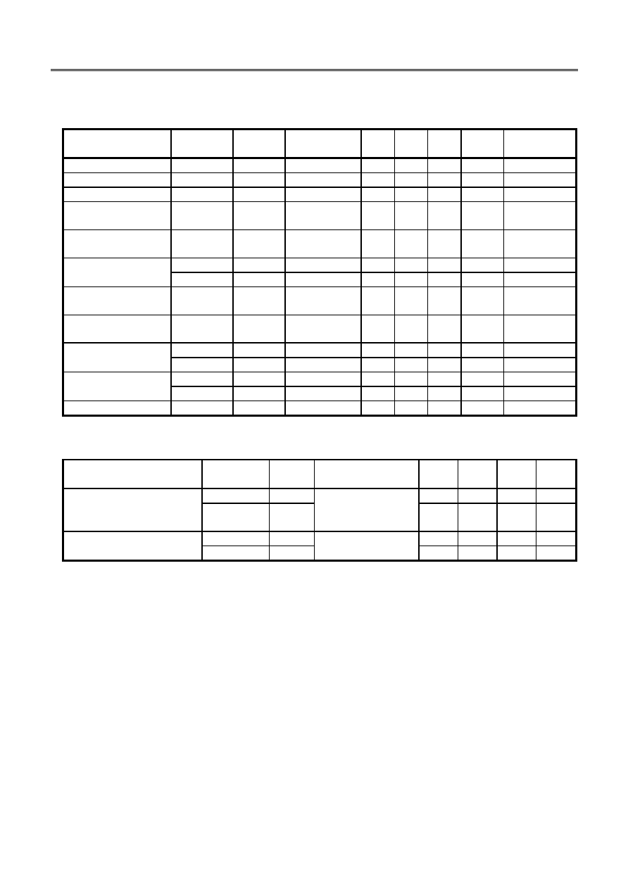
Electrical Characteristics
1. V
DD
= 5.0 V
DC Characteristics (V
DD
= 5.0 V)
Table 5
(Ta
= 25°C unless otherwise specified)
Parameter
Model No.
Symbol
Measurement
Conditions
Min.
Typ. Max.
Unit
Measurement
Circuit
Input offset voltage
V
IO
±3
±4
mV
Figure 5
Input offset current
I
IO
1
pA
Input bias current
I
BIAS
1
pA
Common-mode input
voltage range
V
CMR
0
4.3
V
Voltage gain
(open loop)
G
V
70
80
dB
Maximum output
V
OH
R
L
= 1.0 M
4.9
V
Figure 7
swing voltage
V
OL
R
L
= 1.0 M
0.1
V
Figure 8
Common-mode input
signal rejection ratio
CMRR
60
70
dB
Figure 6
Power supply voltage
rejection ratio
PSRR
60
70
dB
Figure 5
S-89110A
I
DD
50
120
µA
Figure 9
S-89120A
I
DD
10
30
µA
Figure 9
S-89110A
I
SOURCE
V
OH
= 0 V
120
µA
Figure 10
S-89120A
I
SOURCE
V
OH
= 0 V
25
µA
Figure 10
Sink current
I
SINK
V
OL
= V
DD
20
mA
Figure 11
AC Characteristics (V
DD
= 5.0 V)
Table 6
(Ta
= 25°C unless otherwise specified)
Parameter
Model No.
Symbol
Measurement
Conditions
Min.
Typ.
Max.
Unit
S-89110A
SR
R
L
= 1.0 M
0.07
V/
µs
Slew rate
S-89120A
SR
C
L
= 15 pF
(Refer to Figure 12.)
0.015
V/
µs
S-89110A
GBP
180
kHz
S-89120A
GBP
40
kHz
Supply current
Source current
Gain-bandwidth product
CMOS SINGLE OPERATIONAL AMPLIFIER
Rev. 1.2
_10
S-891xxA Series
4
Seiko Instruments Inc.
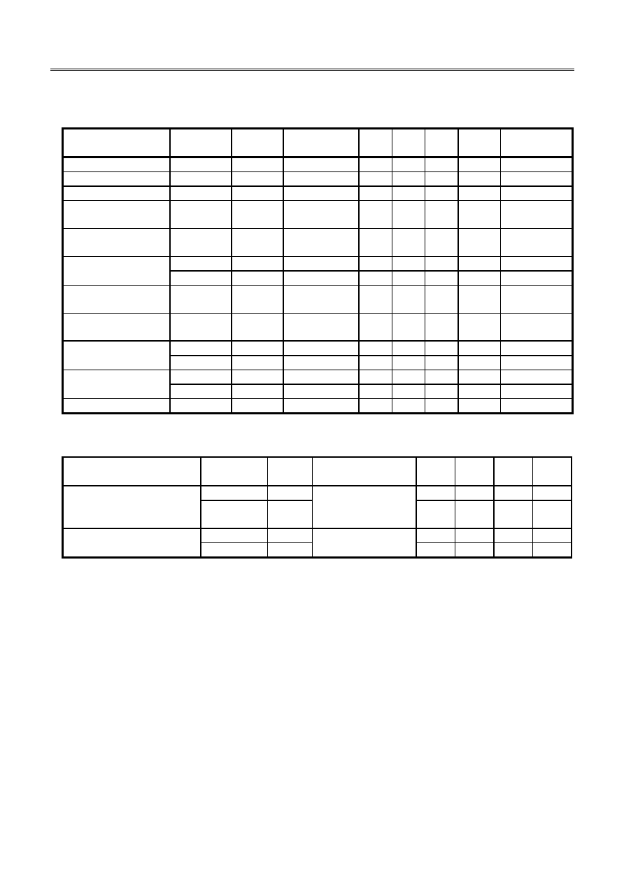
2. V
DD
= 3.0 V
DC Characteristics (V
DD
= 3.0 V)
Table 7
(Ta
= 25°C unless otherwise specified)
Parameter
Model No.
Symbol
Measurement
Conditions
Min.
Typ. Max.
Unit
Measurement
Circuit
Input offset voltage
V
IO
±3
±4
mV
Figure 5
Input offset current
I
IO
1
pA
Input bias current
I
BIAS
1
pA
Common-mode input
voltage range
V
CMR
0
2.3
V
Voltage gain
(open loop)
G
V
70
80
dB
Maximum output
V
OH
R
L
= 1.0 M
2.9
V
Figure 7
swing voltage
V
OL
R
L
= 1.0 M
0.1
V
Figure 8
Common-mode input
signal rejection ratio
CMRR
60
70
dB
Figure 6
Power supply voltage
rejection ratio
PSRR
60
70
dB
Figure 5
S-89110A
I
DD
50
120
µA
Figure 9
S-89120A
I
DD
10
30
µA
Figure 9
S-89110A
I
SOURCE
V
OH
= 0 V
120
µA
Figure 10
S-89120A
I
SOURCE
V
OH
= 0 V
25
µA
Figure 10
Sink current
I
SINK
V
OL
= V
DD
15
mA
Figure 11
AC Characteristics (V
DD
= 3.0 V)
Table 8
(Ta
= 25°C unless otherwise specified)
Parameter
Model No.
Symbol
Measurement
Conditions
Min.
Typ.
Max.
Unit
S-89110A
SR
R
L
= 1.0 M
0.07
V/
µs
Slew rate
S-89120A
SR
C
L
= 15 pF
(Refer to Figure 12.)
0.015
V/
µs
S-89110A
GBP
175
kHz
S-89120A
GBP
35
kHz
Supply current
Source current
Gain-bandwidth product
Rev.1.2
_10
CMOS SINGLE OPERATIONAL AMPLIFIER
S-891xxA Series
Seiko Instruments Inc.
5
3. V
DD
= 1.8 V
DC Characteristics (V
DD
= 1.8 V)
Table 9
(Ta
= 25°C unless otherwise specified)
Parameter
Model No.
Symbol
Measurement
Conditions
Min.
Typ. Max.
Unit
Measurement
Circuit
Input offset voltage
V
IO
±3
±4
mV
Figure 5
Input offset current
I
IO
1
pA
Input bias current
I
BIAS
1
pA
Common-mode input
voltage range
V
CMR
0
1.1
V
Voltage gain
(open loop)
G
V
70
80
dB
Maximum output
V
OH
R
L
= 1.0 M
1.7
V
Figure 7
swing voltage
V
OL
R
L
= 1.0 M
0.1
V
Figure 8
Common-mode input
signal rejection ratio
CMRR
60
70
dB
Figure 6
Power supply voltage
rejection ratio
PSRR
60
70
dB
Figure 5
S-89110A
I
DD
50
120
µA
Figure 9
S-89120A
I
DD
10
30
µA
Figure 9
S-89110A
I
SOURCE
V
OH
= 0 V
100
µA
Figure 10
S-89120A
I
SOURCE
V
OH
= 0 V
20
µA
Figure 10
Sink current
I
SINK
V
OL
= V
DD
5
mA
Figure 11
AC Characteristics (V
DD
= 1.8 V)
Table 10
(Ta
= 25°C unless otherwise specified)
Parameter
Model No.
Symbol
Measurement
Conditions
Min.
Typ.
Max.
Unit
S-89110A
SR
R
L
= 1.0 M
0.07
V/
µs
Slew rate
S-89120A
SR
C
L
= 15 pF
(Refer to Figure 12.)
0.015
V/
µs
S-89110A
GBP
160
kHz
S-89120A
GBP
30
kHz
Supply current
Source current
Gain-bandwidth product