 | –≠–Ľ–Ķ–ļ—ā—Ä–ĺ–Ĺ–Ĺ—č–Ļ –ļ–ĺ–ľ–Ņ–ĺ–Ĺ–Ķ–Ĺ—ā: S-89431A | –°–ļ–į—á–į—ā—Ć:  PDF PDF  ZIP ZIP |
Rev.1.1
_20
MINI ANALOG SERIES
0.5
Ķ
Ķ
Ķ
ĶA Rail-to-Rail CMOS OPERATIONAL AMPLIFIER
S-8943xA/B Series
Seiko Instruments Inc.
1
The mini-analog series is a group of ICs that incorporate a
general-purpose analog circuit in an ultra-small package.
The S-8943xA/B series are CMOS type operational amplifiers that
feature Rail-to-Rail* I/O and an internal phase compensation
circuit. These features enable driving at a lower voltage (from 0.9
V) and with lower current consumption (0.5
ĶA typ.) than existing
general-purpose operational amplifiers, making the S-8943xA/B
series ideal for use in battery-powered compact portable devices.
The S-8943xA series is a single operational amplifier, with one
circuit incorporated in the ultra-small SC-88A. The S-8943xB
series is a dual operational amplifier, with two circuits
incorporated in the slim and small 8-pin SON(A) package and 8-
pin MSOP package.
* Rail-to-Rail is a registered trademark of Motorola Inc.
Features
∑ Can be driven at lower voltage than existing general-purpose
operational amplifiers: V
DD
= 0.9 to 5.5 V
∑ Ultra-low current consumption: I
DD
= 0.5 ĶA (typ.)
∑ Rail-to-rail wide I/O voltage range: V
CMR
= V
SS
to V
DD
∑ Low input offset voltage: 5.0 mV (max.)
∑ No external devices required due to an internal phase compensation
∑ Small package:
5-Pin SC-88A
2.0 mm
◊ 2.1 mm
8-Pin SON(A)
2.9 mm
◊ 3.0 mm
8-Pin MSOP
2.95 mm
◊ 4.0 mm
Packages
∑ 5-pin SC-88A (package drawing code: NP005-B)
∑ 8-pin SON(A) (package drawing code: PN008-A)
∑ 8-pin MSOP (package drawing code: FN008-A)
Selection Guide
Table 1
Package
SC-88A
8-Pin SON (A)
8-Pin MSOP
Input Offset Voltage
Product Name (Single)
Product Name (Dual)
Product Name (Dual)
V
IO
= 10 mV max.
S-89430ACNC-HBU-TF
S-89430BCPN-HEU-TF
S-89430BCFN-HEU-T2
V
IO
= 5 mV max.
S-89431ACNC-HBV-TF
S-89431BCPN-HEV-TF
S-89431BCFN-HEV-T2
Applications
∑ Cellular phones
∑ PDAs
∑ Notebook PCs
∑ Digital cameras
∑ Digital camcorders

0.5
ĶA Rail-to-Rail
CMOS OPERATIONAL AMPLIFIER
Rev.1.1
_20
S-8943xA/B Series
Seiko Instruments Inc.
2
Pin Configurations
(S-8943xACNC)
5-Pin SC-88A
Top View
VSS
IN(
+
+
+
+)
IN(
-
-
-
-)
VDD
OUT
1
2
3
5
4
Figure 1
(S-8943xBCPN)
8-Pin SON(A)
Top View
VSS
IN1(
+
+
+
+)
IN1(
-
-
-
-)
IN2(
+
+
+
+)
IN2(
-
-
-
-)
VDD
OUT1
OUT2
1
2
3
5
4
8
7
6
Figure 2
(S-8943xBCFN)
8-Pin MSOP
Top View
VSS
VDD
IN2(
+
+
+
+)
IN2(
-
-
-
-)
IN1(
+
+
+
+)
IN1(
-
-
-
-)
OUT2
OUT1
4
3
2
8
7
6
5
1
Figure 3
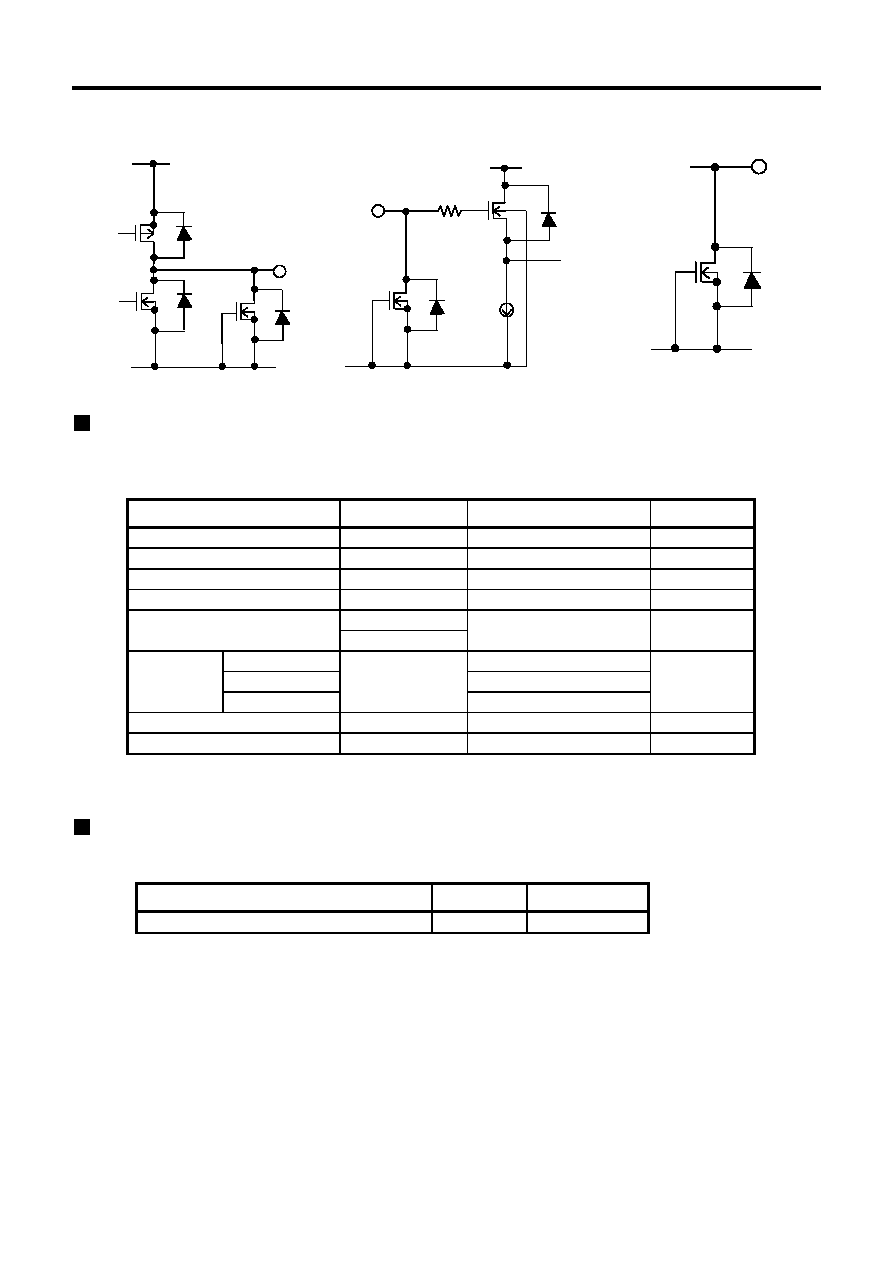
Table 2 Pin Descriptions
(S-8943xACNC)
Table 4 Pin Descriptions
(S-8943xBCFN)
Pin No. Symbol
Function
Internal Equivalent
Circuit
1
IN(
+) Non-inverted input pin
Figure 5
2
VSS GND pin
3
IN(
-) Inverted input pin
Figure 5
4
OUT Output pin
Figure 4
5
VDD Positive power pin
Figure 6
Pin No. Symbol
Function
Internal Equivalent
Circuit
1
IN1(
-) Inverted input pin 1
Figure 5
2
IN1(
+) Non-inverted input pin 1
Figure 5
3
IN2(
-) Inverted input pin 2
Figure 5
4
IN2(
+) Non-inverted input pin 2
Figure 5
5
VSS GND pin
6
OUT2 Output pin 2
Figure 4
7
VDD Positive power pin
Figure 6
8
OUT1 Output pin 1
Figure 4
Pin No. Symbol
Function
Internal Equivalent
Circuit
1
OUT1 Output pin 1
Figure 4
2
VDD Positive power pin
Figure 6
3
OUT2 Output pin 2
Figure 4
4
VSS GND pin
5
IN2(
+) Non-inverted input pin 2
Figure 5
6
IN2(
-) Inverted input pin 2
Figure 5
7
IN1(
+) Non-inverted input pin 1
Figure 5
8
IN1(
-) Inverted input pin 1
Figure 5
Table 3 Pin Descriptions
(S-8943xBCPN)
Rev.1.1
_20
0.5
ĶA Rail-to-Rail
CMOS OPERATIONAL AMPLIFIER
S-8943xA/B Series
Seiko Instruments Inc.
3
[Internal equivalent circuits]
<1> Output pin
<2> Input pin
<3> VDD pin
VDD
VSS
VSS
VDD
VSS
VDD
Figure 4
Figure 5
Figure 6
Absolute Maximum Ratings
Table 5
(Ta
= 25įC unless otherwise specified)
Parameter
Symbol
Ratings
Unit
Power supply voltage
V
DD
- V
SS
7.0
V
Input voltage
V
IN
V
SS
to V
DD
V
Output voltage
V
OUT
V
SS
to V
DD
V
Differential input voltage
V
IND
Ī5.5
V
I
SOURCE
I
SINK
SC-88A
200
8-pin SON (A)
P
D
300
mW
8-pin MSOP
300
Operating temperature
T
opr
-40 to +85
įC
Storage temperature
T
stg
-55 to +125
įC
Caution: Although the IC contains a static electricity protection circuit, excessive static electricity
or voltage exceeding the limit of the protection circuit should not be applied.
Recommended Operating Power Supply Voltage Range
Table 6
Item
Symbol
Range
Operational power supply voltage range
V
DD
0.9 to 5.5 V
Output pin current
7
mA
Power
dissipation
0.5
ĶA Rail-to-Rail
CMOS OPERATIONAL AMPLIFIER
Rev.1.1
_20
S-8943xA/B Series
Seiko Instruments Inc.
4
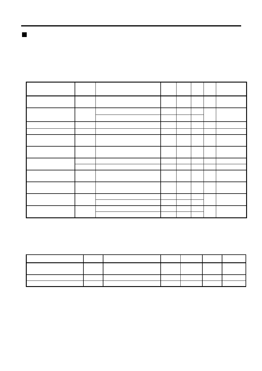
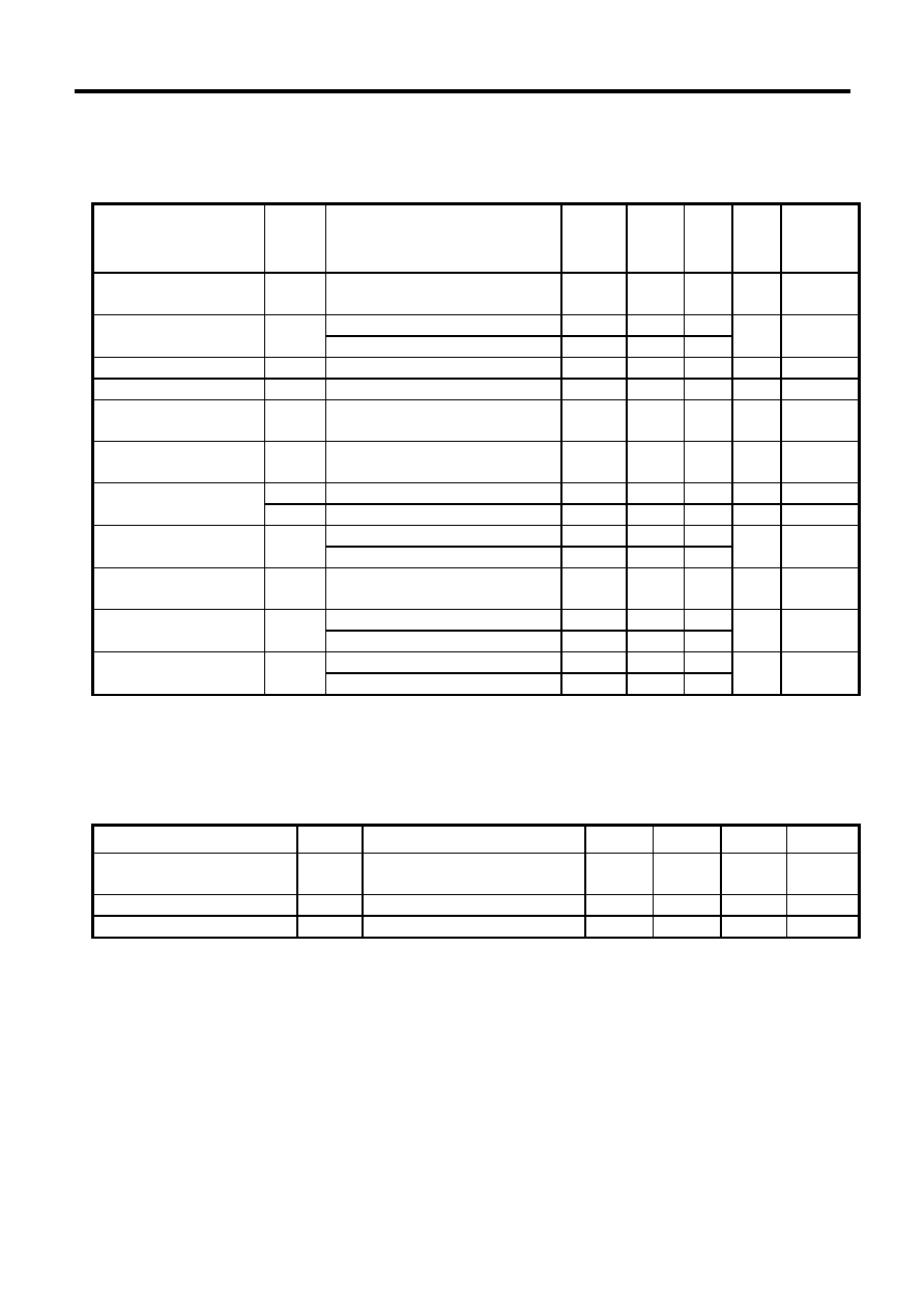
Electrical Characteristics
S-89430ACNC and S-89431ACNC, S-89430BCPN and S-89431BCPN, and S-89430BCFN and
S-89431BCFN, differ only in the input offset voltage; all other specifications are the same.
1. V
DD
= 3.0 V
Table 7
DC Characteristics (V
DD
= 3.0 V )
(Ta
= 25įC unless otherwise specified)
Parameter
Symbol
Measurement Conditions
Min.
Typ. Max. Unit Measurement
Circuit
Power supply current
*1
(per circuit)
I
DD
V
CMR
= V
OUT
= 1.5 V
0.5
0.9
ĶA
Figure 12
S-89430A/B: V
CMR
= 1.5 V
-10
Ī5
+10
S-89431A/B: V
CMR
= 1.5 V
-5
Ī3
+5
Input offset current
I
IO
1
pA
Input bias current
I
BIAS
1
pA
Common-mode input
voltage
V
CMR
0
3.0
V
Voltage gain
(open loop)
A
VOL
V
SS
+ 0.1 V V
OUT
V
DD
- 0.1 V;
V
CMR
= 1.5 V, R
L
= 1 M
70
80
dB
Figure 16
Maximum output
V
OH
R
L
= 100 k
2.95
V
Figure 10
swing voltage
V
OL
R
L
= 100 k
0.05
V
Figure 11
Common mode input
signal rejection ratio
CMRR
45
65
dB
Figure 9
Power supply voltage
rejection ratio
PSRR
V
DD
= 0.9 to 5.5 V
70
80
dB
Figure 7
V
OUT
= V
DD
- 0.1 V
400
500
V
OUT
= 0 V
4800
6000
V
OUT
= 0.1 V
400
550
V
OUT
= V
DD
4800
6000
*1 When the output is saturated on the V
DD
side, a power supply current of up to 3 to 5
ĶA may flow.
(Refer to 4. Power supply current vs. Common-mode input voltage characteristics in the operational
amplifier characteristics graphs.)
Table 8
AC Characteristics (V
DD
= 3.0 V)
(Ta
= 25įC unless otherwise specified)
Parameter
Symbol
Measurement Conditions
Min.
Typ.
Max.
Unit
Slew rate
SR
R
L
= 1.0 M, C
L
= 15 pF
(Refer to Figure 15.)
5
V/ms
Gain-bandwidth product
GBP
C
L
= 0 pF
4.8
kHz
Maximum load capacitance
C
L
47
pF
ĶA
ĶA
Figure 8
Figure 13
Figure 14
mV
Input offset voltage
Source current
Sink current
V
IO
V
SS
V
CMR
V
DD
I
SOURCE
I
SINK
Rev.1.1
_20
0.5
ĶA Rail-to-Rail
CMOS OPERATIONAL AMPLIFIER
S-8943xA/B Series
Seiko Instruments Inc.
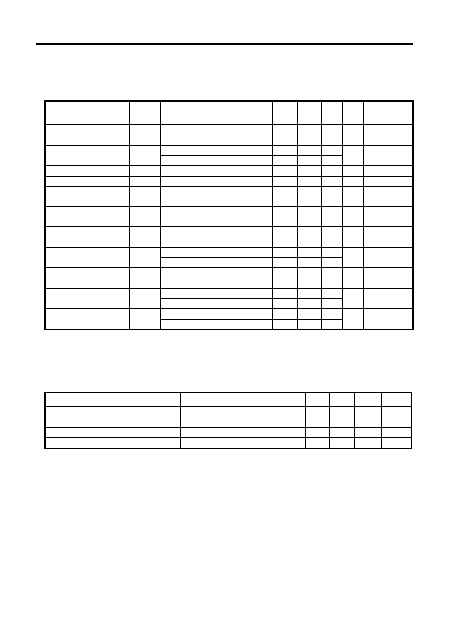
5
2. V
DD
= 1.8 V
Table 9
DC Characteristics (V
DD
= 1.8 V)
(Ta
= 25įC unless otherwise specified)
Parameter
Symbol
Measurement Conditions
Min.
Typ. Max. Unit Measurement
Circuit
Power supply current
*1
(per circuit)
I
DD
V
CMR
= V
OUT
= 0.9 V
0.5
0.9
ĶA
Figure 12
S-89430A/B: V
CMR
= 0.9 V
-10
Ī5
+10
S-89431A/B: V
CMR
= 0.9 V
-5
Ī3
+5
Input offset current
I
IO
1
pA
Input bias current
I
BIAS
1
pA
Common-mode input
voltage
V
CMR
0
1.8
V
Voltage gain
(open loop)
A
VOL
V
SS
+ 0.1 V V
OUT
V
DD
- 0.1 V;
V
CMR
= 0.9 V, R
L
= 1 M
66
75
dB
Figure 16
Maximum output
V
OH
R
L
= 100 k
1.75
V
Figure 10
swing voltage
V
OL
R
L
= 100 k
0.05
V
Figure 11
Common-mode input
V
SS
V
CMR
V
DD
35
55
signal rejection ratio
V
SS
V
CMR
V
DD
- 0.3 V
45
60
Power supply voltage
rejection ratio
PSRR
V
DD
= 0.9 to 5.5 V
70
80
dB
Figure 7
V
OUT
= V
DD
- 0.1 V
220
300
V
OUT
= 0 V
1200 1800
V
OUT
= 0.1 V
220
300
V
OUT
= V
DD
1200 1800
*1
When the output is saturated on the V
DD
side, a power supply current of up to 3 to 5
ĶA may flow.
(Refer to 4. Power supply current vs. Common-mode input voltage characteristics in the operational
amplifier characteristics graphs. )
Table 10
AC Characteristics (V
DD
= 1.8 V)
(Ta
= 25įC unless otherwise specified)
Parameter
Symbol
Measurement Conditions
Min.
Typ.
Max.
Unit
R
L
= 1.0 M, C
L
= 15 pF
(Refer to Figure 15.)
Gain-bandwidth product
GBP
C
L
= 0 pF
5
kHz
Maximum load capacitance
C
L
47
pF
Figure 8
Input offset voltage
V
IO
mV
Figure 9
Figure 13
Figure 14
ĶA
ĶA
CMRR
I
SOURCE
I
SINK
Sink current
Source current
4.5
V/ms
SR
Slew rate
dB
0.5
ĶA Rail-to-Rail
CMOS OPERATIONAL AMPLIFIER
Rev.1.1
_20
S-8943xA/B Series
Seiko Instruments Inc.
6
3. V
DD
= 0.9 V
Table 11
DC Characteristics (V
DD
= 0.9 V)
(Ta
= 25įC unless otherwise specified)
Item
Symbol
Measurement Conditions
Min.
Typ.
Max.
Unit Measure-
ment
Circuit
Power supply current
*1
(per circuit)
S-89430A/B: V
CMR
= 0.45 V
-10
Ī5
+10
S-89431A/B: V
CMR
= 0.45 V
-5
Ī3
+5
Input offset current
I
IO
1
pA
Input bias current
I
BIAS
1
pA
Common-mode input
voltage
Voltage gain
(open loop)
A
VOL
V
SS
+ 0.1 V V
OUT
V
DD
- 0.1 V;
V
CMR
= 0.45 V, R
L
= 1 M
Maximum output
V
OH
R
L
= 100 k
0.85
V
Figure 10
swing voltage
V
OL
R
L
= 100 k
0.05
V
Figure 11
Common-mode input
V
SS
V
CMR
V
DD
25
55
signal rejection ratio
V
SS
V
CMR
V
DD
- 0.35 V
40
60
Power supply voltage
rejection ratio
V
OUT
= V
DD
- 0.1 V
25
65
V
OUT
= 0 V
40
140
V
OUT
= 0.1 V
10
65
V
OUT
= V
DD
12
120
*1
When the output is saturated on the V
DD
side, a power supply current of up to 3 to 5
ĶA may flow.
(Refer to 4. Power supply current vs. Common-mode input voltage characteristics in the operational
amplifier characteristics graphs.)
Table 12
AC Characteristics (V
DD
= 0.9 V)
(Ta
= 25įC unless otherwise specified)
Item
Symbol
Measurement Conditions
Min.
Typ.
Max.
Unit
R
L
= 1.0 M, C
L
= 15 pF
(Refer to Figure 15.)
Gain-bandwidth product
GBP
C
L
= 0 pF
5
kHz
Maximum load capacitance
C
L
47
pF
ĶA
ĶA
ĶA
Figure 12
Figure 8
mV
V
CMR
= V
OUT
= 0.45 V
I
DD
V
IO
Input offset voltage
V
CMR
0
0.9
V
60
75
Figure 16
Figure 9
Figure 7
Figure 13
Figure 14
dB
dB
dB
CMRR
PSRR
V
DD
= 0.9 to 5.5 V
Source current
Sink current
I
SOURCE
I
SINK
70
80
SR
Slew rate
4
V/ms
0.5
0.9
Rev.1.1
_20
0.5
ĶA Rail-to-Rail
CMOS OPERATIONAL AMPLIFIER
S-8943xA/B Series
Seiko Instruments Inc.
7
Measurement Circuits
1. Power supply voltage rejection ratio
∑ Power supply voltage rejection ratio (PSRR)
The power supply rejection ratio (PSRR) can be
calculated by the following formula, with the value of
V
OUT
measured at each V
DD
.
Measurement conditions:
When V
DD
= 0.9 V: V
DD
= V
DD1
, V
OUT
= V
OUT1
When V
DD
= 5.5 V: V
DD
= V
DD2
, V
OUT
= V
OUT2
+
◊
-
-
=
S
S
F
OUT2
OUT1
DD2
DD1
R
R
R
V
V
V
V
20log
PSRR
Figure 7
2. Input offset voltage
∑ Input offset voltage (V
IO
)
S
F
S
DD
OUT
IO
R
R
R
2
V
V
V
+
-
=
◊
Figure 8
R
F
R
S
R
S
R
F
+
-
V
OUT
V
DD
0.45 V
R
F
R
S
R
S
R
F
+
-
V
OUT
V
DD
V
CMR
= V
DD
/2

0.5
ĶA Rail-to-Rail
CMOS OPERATIONAL AMPLIFIER
Rev.1.1
_20
S-8943xA/B Series
Seiko Instruments Inc.
8
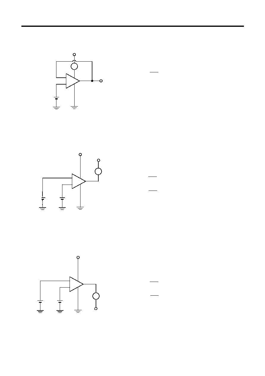
3. Common-mode input signal rejection ratio, common-mode input voltage
∑ Common-mode input signal rejection ratio (CMRR)
The common-mode input signal rejection ratio (CMRR)
can be calculated by the following formula, with the value
of V
OUT
measured at each V
IN.
Measurement conditions:
When V
IN
= V
CMR
(Max.): V
IN
= V
IN1
, V
OUT
= V
OUT1
When V
IN
= V
CMR
(Min.): V
IN
= V
IN2
, V
OUT
= V
OUT2
(
)
+
◊
-
-
=
S
S
F
OUT2
OUT1
IN2
IN1
R
R
R
V
V
V
V
20log
CMRR
∑ Common-mode input voltage (V
CMR
)
The common-mode input voltage (V
CMR
) is the range of
input voltage within which V
OUT
satisfies the common-
mode rejection ratio specification when V
IN2
is varied.
4. Maximum output swing voltage
∑ Maximum output swing voltage (V
OH
)
Measurement conditions:
V
0.1
2
V
V
DD
IN1
-
=
V
0.1
2
V
V
DD
IN2
+
=
R
L
= 100 k
Figure 10
∑ Maximum output swing voltage (V
OL
)
Measurement conditions:
V
0.1
2
V
V
DD
IN1
+
=
V
0.1
2
V
V
DD
IN2
-
=
R
L
= 100 k
Figure 11
R
F
R
S
R
S
R
F
+
-
V
OUT
V
DD
V
DD
/2
V
IN
V
IN2
+
-
V
OH
V
DD
/2
V
DD
R
L
V
IN1
V
IN2
+
-
V
OL
V
DD
/2
V
DD
R
L
V
IN1
Figure 9
Rev.1.1
_20
0.5
ĶA Rail-to-Rail
CMOS OPERATIONAL AMPLIFIER
S-8943xA/B Series
Seiko Instruments Inc.
9
5. Power supply current
∑ Power supply current (I
DD
)
Measurement conditions:
2
V
V
DD
CMR
=
Figure 12
6. Source current
∑ Source current (I
SOURCE
)
Measurement conditions:
V
OUT
= V
DD
- 0.1 V or V
OUT
= 0 V
V
0.1
2
V
V
DD
IN1
-
=
V
0.1
2
V
V
DD
IN2
+
=
Figure 13
7. Sink current
∑ Sink current (I
SINK
)
Measurement conditions:
V
OUT
= 0.1 V or V
OUT
= V
DD
V
0.1
2
V
V
DD
IN1
+
=
V
0.1
2
V
V
DD
IN2
-
=
Figure 14
V
CMR
= V
DD
/ 2
+
-
V
OUT
V
DD
A
+
-
V
OUT
V
DD
V
IN1
A
V
IN2
V
IN2
+
-
V
OUT
V
DD
A
V
IN1
0.5
ĶA Rail-to-Rail
CMOS OPERATIONAL AMPLIFIER
Rev.1.1
_20
S-8943xA/B Series
Seiko Instruments Inc.
10
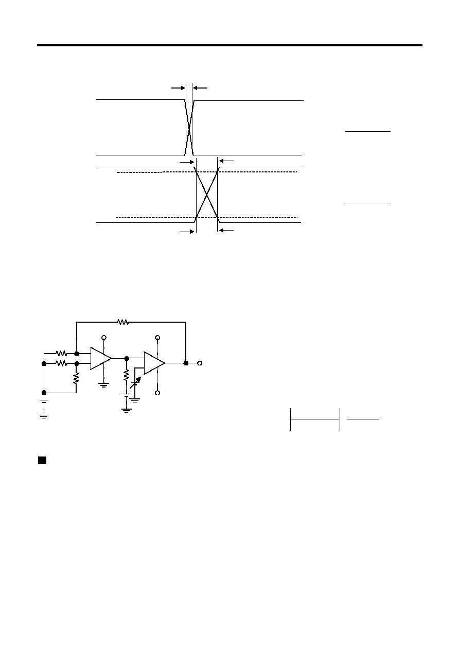
8. Slew rate (SR)
V
OUT
V
OUT
IN(
+) = V
DD
IN(
+) = 0 V
t
TLH
t
THL
V
OH
V
OL
t
R
= t
F
= 1 Ķs (0 V to V
DD
)
When rising
When falling
V
OH
- V
OL
t
THL
SR
=
V
OH
- V
OL
t
TLH
SR
=
Figure 15
V
OH
= 2.7 V (when V
DD
= 3.0 V), 1.62 V (when V
DD
= 1.8 V), 0.81 V (when V
DD
= 0.9 V)
V
OL
= 0.3 V (when V
DD
= 3.0 V), 0.18 V (when V
DD
= 1.8 V), 0.09 V (when V
DD
= 0.9 V)
9. Voltage gain (open loop)
∑ Voltage gain (open loop) (A
VOL
)
The voltage gain (A
VOL
) can be calculated by the
following formula, with the value of V
OUT
measured at
each V
M
.
Measurement conditions:
When V
M
= V
DD
- 0.1 V: V
M
= V
M1
, V
OUT
= V
OUT1
When V
M
= 0.1 V: V
M
= V
M2
, V
OUT
= V
OUT2
(
)
-
=
+
◊
-
S
S
F
OUT2
OUT1
M2
M1
VOL
R
R
R
V
V
V
V
20log
A
Figure 16
Cautions
∑ Note that when the output is saturated on the V
DD
side, a power supply current of up to 3 to 5
ĶA may flow.
(Refer to 4. Power Supply Current vs. Common-mode input voltage characteristics in the operational
amplifier characteristics graphs.)
∑ Be sure to use the product with an output current of no more than 7 mA
R
F
R
S
R
S
R
F
V
DD
V
DD
/2
1 M
V
CMR
= V
DD
/2
V
M
+
-
NULL
V
OUT
V
SSN
V
DDN
D.U.T
+
-
Rev.1.1
_20
0.5
ĶA Rail-to-Rail
CMOS OPERATIONAL AMPLIFIER
S-8943xA/B Series
Seiko Instruments Inc.
11
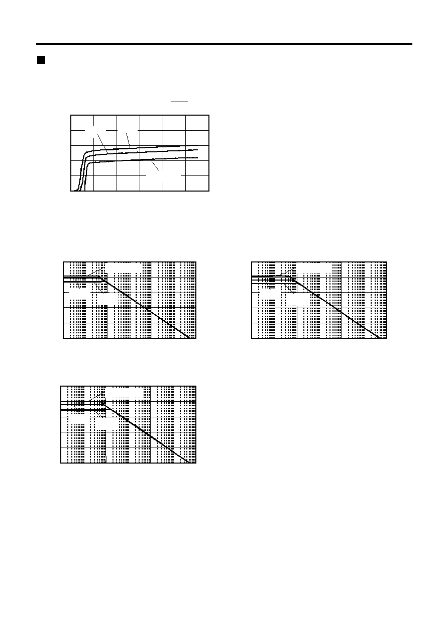
Operational Amplifier Characteristics
(All Data Indicates Typical Values for One Circuit)
1. Power supply current vs. Power supply voltage
0.0
0.2
0.4
0.6
0.8
1.0
0
1
2
3
4
5
6
V
DD
(V)
I
DD
(
Ķ
A)
25
įC
Ta
= -40įC
85
įC
2. Voltage gain vs. Frequency
V
DD
= 3 V, V
SS
= 0 V
V
DD
= 1.8 V, V
SS
= 0 V
0
20
40
60
80
100
1.E
-02
1.E
+00
1.E
+02
1.E
+04
f (Hz)
Ga
i
n
(dB
)
25
įC
85
įC
Ta
= -40įC
0
20
40
60
80
100
1.E
-02
1.E
+00
1.E
+02
1.E
+04
f (Hz)
Ga
i
n
(dB
)
25
įC
85
įC
Ta
= -40įC
V
DD
= 0.9 V, V
SS
= 0 V
0
20
40
60
80
100
1.E
-02
1.E
+00
1.E
+02
1.E
+04
f (Hz)
Ga
i
n
(dB
)
25
įC
85
įC
Ta
= -40įC
V
DD
2
V
SS
= 0 V, V
CMR
= V
OUT
=
0.5
ĶA Rail-to-Rail
CMOS OPERATIONAL AMPLIFIER
Rev.1.1
_20
S-8943xA/B Series
Seiko Instruments Inc.
12
3. Output Current Characteristics
3-1. I
SOURCE
vs. Power supply voltage
I
SINK
vs. Power supply voltage
V
OH
= V
DD
- 0.1 V
V
OL
= 0.1 V
0
500
1000
1500
0
1
2
3
4
5
6
V
DD
(V)
I
SOURCE
(
Ķ
A)
25
įC
85
įC
Ta
= -40įC
0
500
1000
1500
0
1
2
3
4
5
6
V
DD
(V)
I
SI
NK
(
Ķ
A
)
25
įC
85
įC
Ta
= -40įC
3-2. I
SOURCE
vs. Output voltage (V
OH
)
V
DD
= 3.0 V, V
SS
= 0 V
V
DD
= 1.8 V, V
SS
= 0 V
0.0
0.5
1.0
1.5
2.0
2.5
3.0
0
500
1000
1500
2000
I
SOURCE
(
ĶA)
V
OH
(V
)
25
įC
85
įC
Ta
= -40įC
0.0
0.2
0.4
0.6
0.8
1.0
1.2
1.4
1.6
1.8
0
500
1000
1500
2000
I
SOURCE
(
ĶA)
V
OH
(V
)
25
įC
85
įC
Ta
= -40įC
V
DD
= 0.9 V, V
SS
= 0 V
0.0
0.1
0.2
0.3
0.4
0.5
0.6
0.7
0.8
0.9
0
50
100
150
200
I
SOURCE
(
ĶA)
V
OH
(V
)
25
įC
85
įC
Ta
= -40įC
Rev.1.1
_20
0.5
ĶA Rail-to-Rail
CMOS OPERATIONAL AMPLIFIER
S-8943xA/B Series
Seiko Instruments Inc.
13
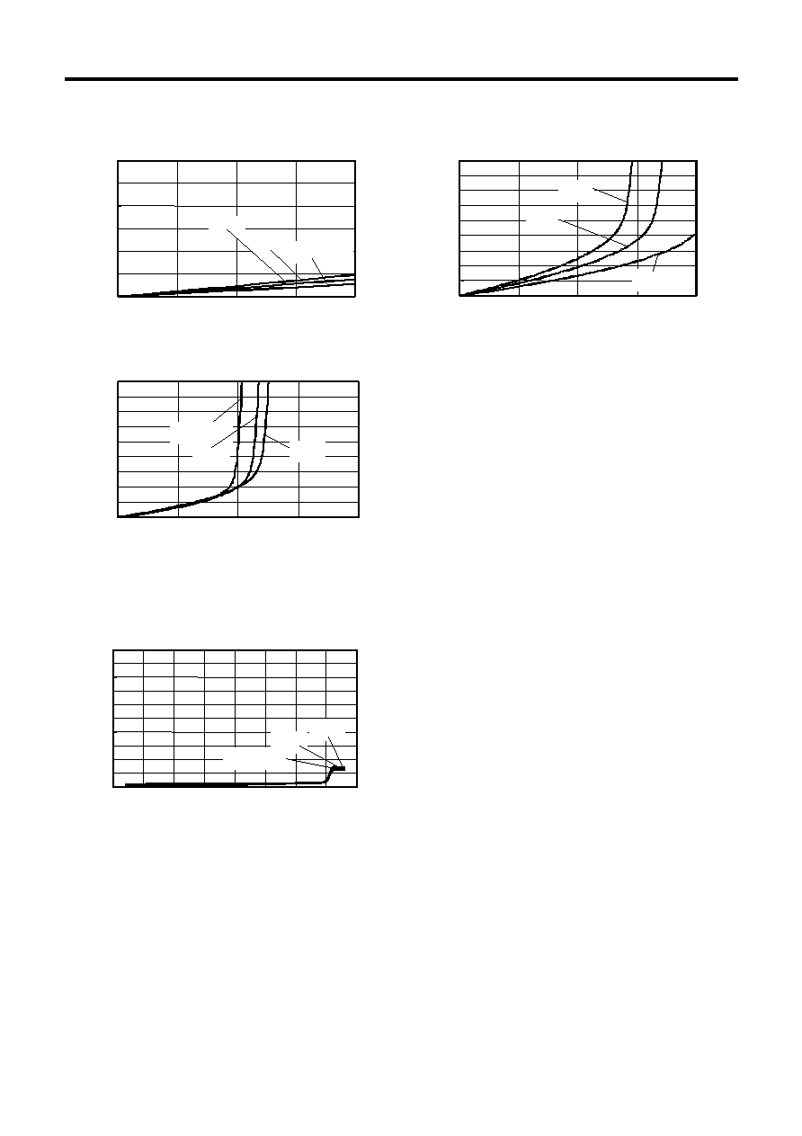
3-3. I
SINK
vs. Output voltage (V
OL
)
V
DD
= 3.0 V, V
SS
= 0 V
V
DD
= 1.8 V, V
SS
= 0 V
0.0
0.5
1.0
1.5
2.0
2.5
3.0
0
500
1000
1500
2000
I
SINK
(
ĶA)
V
OL
(V
)
25
įC
85
įC
Ta
= -40įC
0.0
0.2
0.4
0.6
0.8
1.0
1.2
1.4
1.6
1.8
0
500
1000
1500
2000
I
SINK
(
ĶA)
V
OL
(V
)
25
įC
85
įC
Ta
= -40įC
V
DD
= 0.9 V, V
SS
= 0 V
0.0
0.1
0.2
0.3
0.4
0.5
0.6
0.7
0.8
0.9
0
50
100
150
200
I
SINK
(
ĶA)
V
OL
(V
)
25
įC
85
įC
Ta
= -40įC
4. Power supply current vs. Common-mode input voltage (voltage follower configuration)
V
DD
= 3.0 V, V
SS
= 0 V
0
2
4
6
8
10
12
14
16
18
20
-0.5
0
0.5
1
1.5
2
2.5
3
3.5
V
CMR
(V)
I
DD
(
Ķ
A)
25
įC
85
įC
Ta
= -40įC
2.0Ī0.2
1.3Ī0.1
0.15
+0.1
-0.05
0.65
0.65
1
2
3
4
5
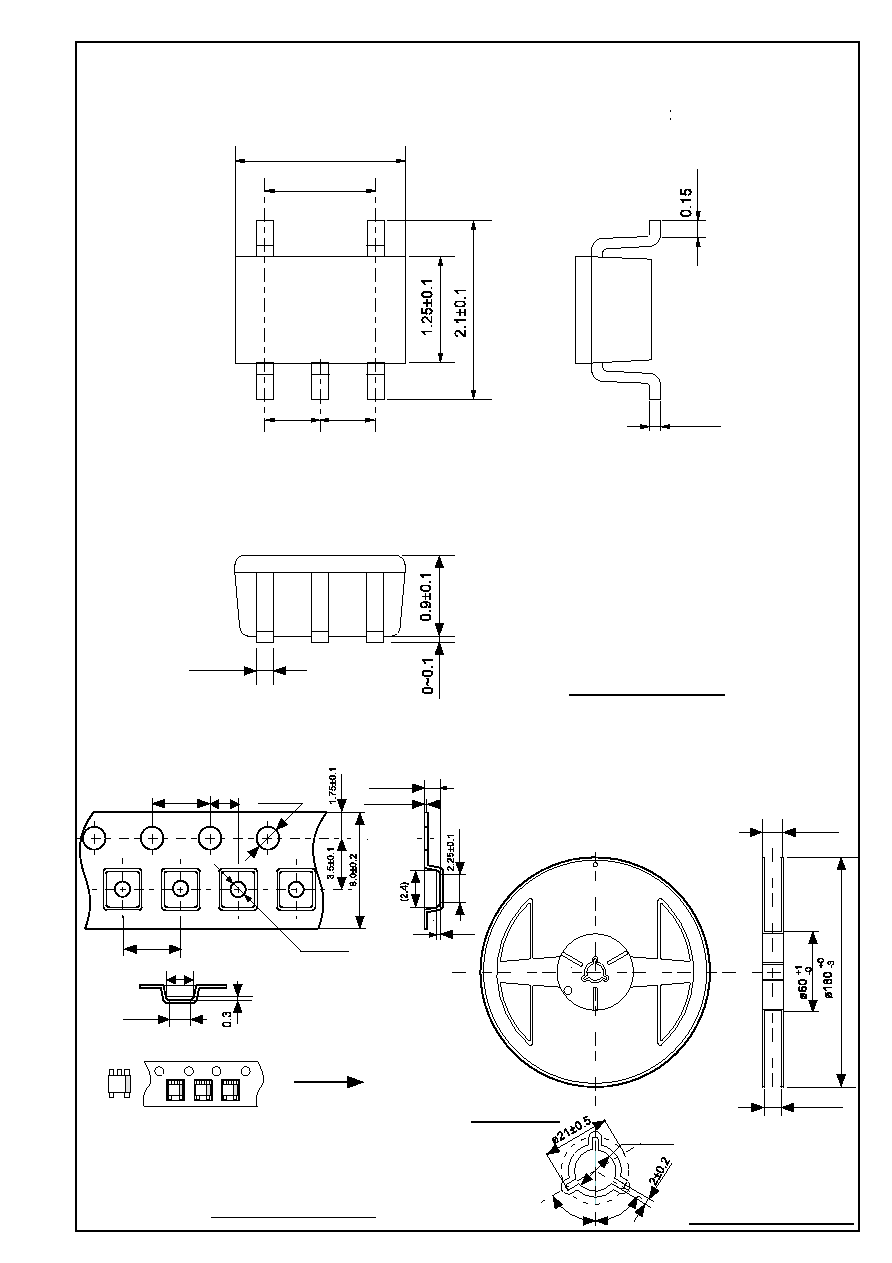
n SC-88A
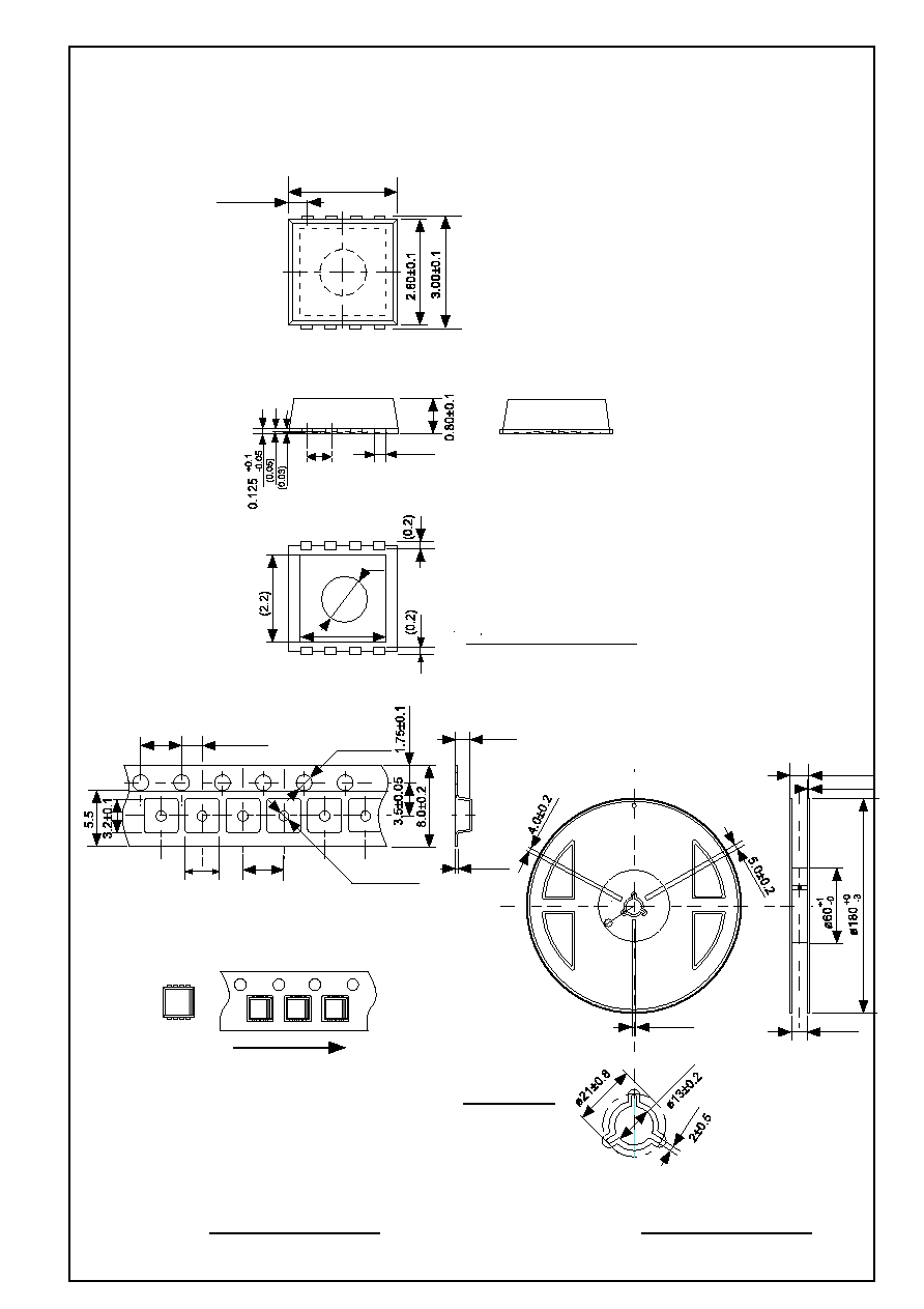
lDimensions
Unit mm
lTaping Specifications
lReel Specifications
No.:NP005-B-P-SD-1.0
NP005-B
Rev.1.1
020517
No. : NP005-B-C-SD-1.0
No. : NP005-B-R-SD-2.0
3000 pcs/reel
(2.25)
4.0Ī0.1 2.0Ī0.1
4.0Ī0.1
Ý1.55Ī0.1
Ý1.05Ī0.1
0.2Ī0.05
1.1Ī0.1
2.05Ī0.1
0.3
TF
1
2
3
4
5
Feed direction
12.5max.
9.0Ī0.3
Ý13Ī0.2
(60į) (60į)
Winding core
0.2
+0.1
-0.05
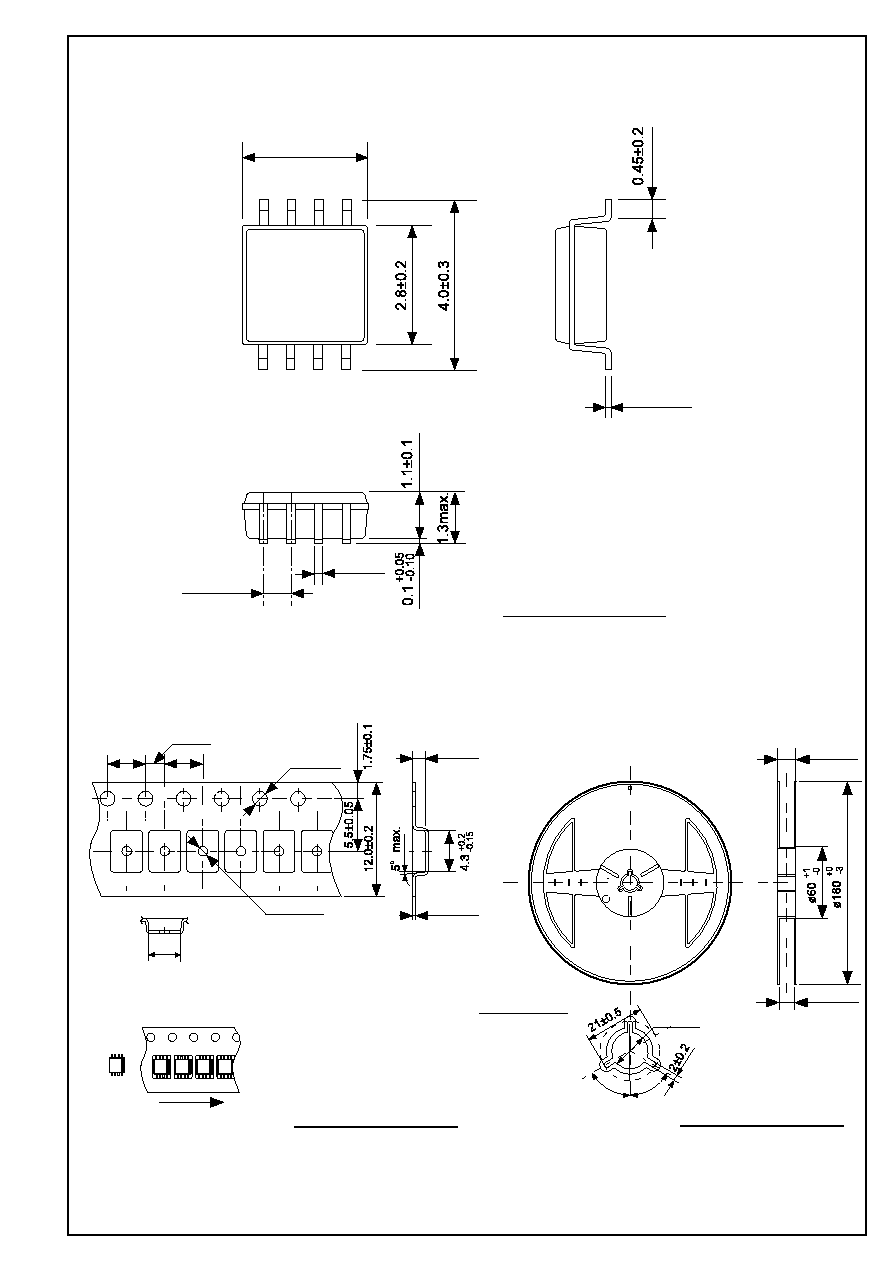
l Reel Specifications
l Tape Specifications
l Dimensions
n SON8A
PN008-A
Rev.1.0
011218
Unit : mm
Ý1.05Ī0.05
0.2Ī0.05
Ý1.55Ī0.05
2.0Ī0.05
4.0Ī0.1
3.3Ī0.1
4.0Ī0.1
TF
1
4
5
8
Feed direction
1.5Ī0.1
No. : PN008-A-C-SD-1.0
2.90Ī0.2
8
5
0.475typ.
1
4
0.30
0.65
+0.1
-0.05
(Ý1.0)
(2.3)
No. : PN008-A-P-SD-1.0
(1.2)
9.0Ī0.3
3.0Ī0.2
11.4Ī1.0
Winding core
No. : PN008-A-R-SD-1.0
3000 pcs/reel
l Reel Specifications
l Tape Specifications
l Dimensions
n 8-Pin MSOP
FN008-A
Rev.1.0
020213
2.95Ī0.2
8
5
0.2Ī0.1
0.65Ī0.1
0.13Ī0.1
1
4
No. : FN008-A-P-SD-1.0
T2
0.3Ī0.05
1.35Ī0.15
1.05Ī0.05
1.55Ī0.05
2.0Ī0.05
4.0Ī0.1
3.1Ī0.15
4.0Ī0.1
1
4
5 8
Feed direction
No. : FN008-A-C-SD-1.0
(60į)
(60į)
13Ī0.2
16.5max.
13.0Ī0.3
Winding core
No. : FN008-A-R-SD-1.0
3000 pcs/reel

∑
The information described herein is subject to change without notice.
∑
Seiko Instruments Inc. is not responsible for any problems caused by circuits or diagrams described herein
whose related industrial properties, patents, or other rights belong to third parties. The application circuit
examples explain typical applications of the products, and do not guarantee the success of any specific
mass-production design.
∑
When the products described herein are regulated products subject to the Wassenaar Arrangement or other
agreements, they may not be exported without authorization from the appropriate governmental authority.
∑
Use of the information described herein for other purposes and/or reproduction or copying without the
express permission of Seiko Instruments Inc. is strictly prohibited.
∑
The products described herein cannot be used as part of any device or equipment affecting the human
body, such as exercise equipment, medical equipment, security systems, gas equipment, or any apparatus
installed in airplanes and other vehicles, without prior written permission of Seiko Instruments Inc.
∑
Although Seiko Instruments Inc. exerts the greatest possible effort to ensure high quality and reliability, the
failure or malfunction of semiconductor products may occur. The user of these products should therefore
give thorough consideration to safety design, including redundancy, fire-prevention measures, and
malfunction prevention, to prevent any accidents, fires, or community damage that may ensue.