S-8953XA_B_E1.2_01
Rev.1.2
_02
MINI ANALOG SERIES
0.7
µ
µ
µ
µA RAIL-TO-RAIL CMOS COMPARATOR
S-8953xA/B Series
Seiko Instruments Inc.
1
The mini analog series is a group of ICs that incorporate a general-
purpose analog circuit in an ultra-small packages.
The S-8953xA/B Series are CMOS type comparators that feature
Rail-to-Rail
*1
I/O and can be driven at a lower voltage and with lower
current consumpsion than existing comparators, making the S-
8953xA/B ideal for use in battery-powered compact portable devices.
*1. Rail-to-Rail is a registered trademark of Motorola Inc.
Features
Applications
Can be driven lower voltage than existing
Cellular phones
general-purpose
comparators:
V
DD
= 0.9 V to 5.5 V
PDAs
Low current consumption:
I
DD
= 0.7 µA (Typ.)
Notebook PCs
Rail-to-Rail
*1
wide input and output voltage range:
Digital cameras
V
CMR
= V
SS
to V
DD
Digital video cameras
Low input offset voltage:
5.0 mV max.
Small package: 5-Pin SC-88A
2.0 mm
× 2.1 mm
8-Pin SON (A)
2.9 mm
× 3.0 mm
Packages
5-Pin SC-88A (package drawing code: NP005-B)
8-Pin SON(A) (package drawing code: PN008-A)
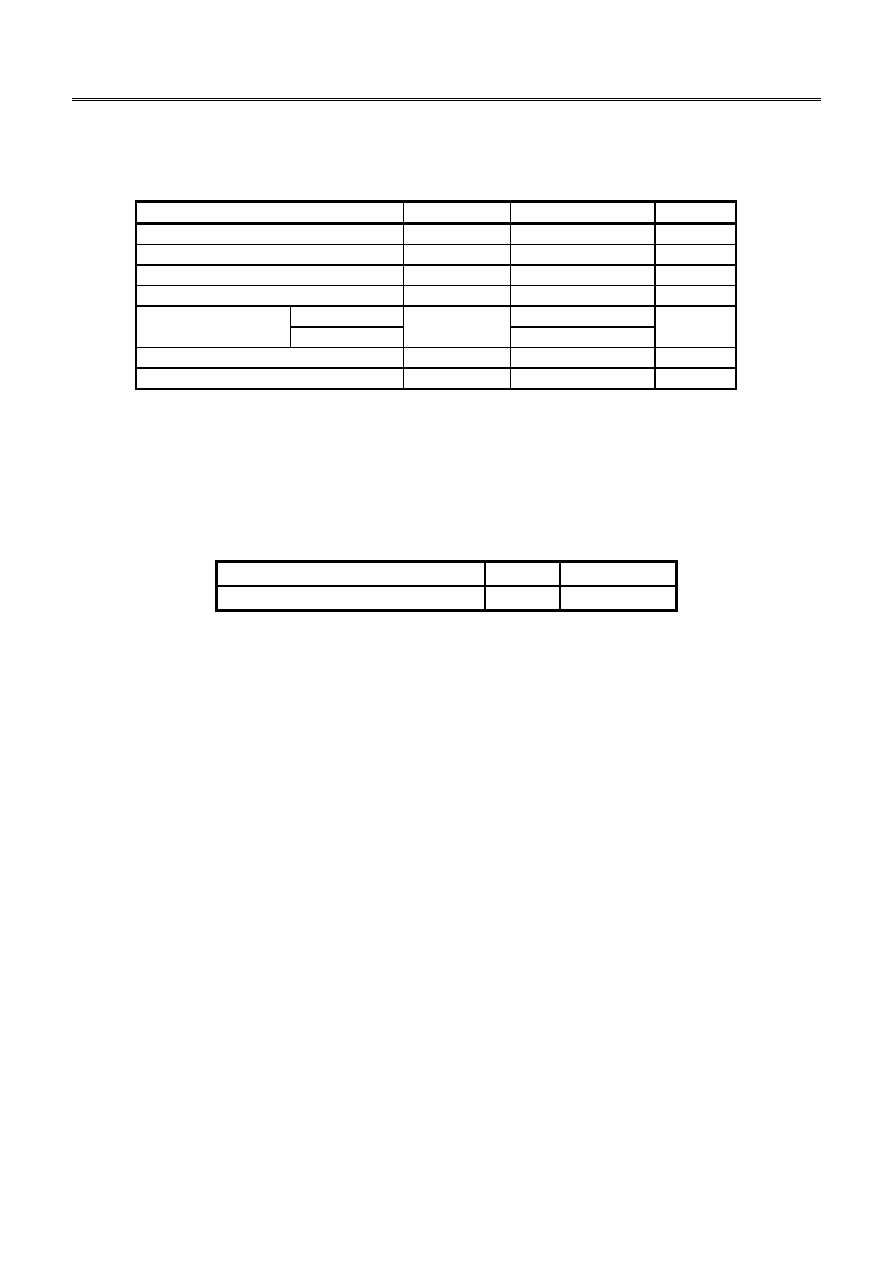
Selection Guide
Table 1
Input Offset Voltage
Product Name (Single)
Product Name (Dual)
V
IO
= 10 mV max.
S-89530ACNC-HCB-TF
S-89530BCPN-HFB-TF
V
IO
= 5 mV max.
S-89531ACNC-HCC-TF
S-89531BCPN-HFC-TF
MINI ANALOG SERIES 0.7
µA RAIL-TO-RAIL CMOS COMPARATOR
Rev.1.2
_02
S-8953xA/B Series
2
Seiko Instruments Inc.
Absolute Maximum Ratings
Table 2
(Ta
= 25°C unless otherwise specified)
Parameter Symbol
Ratings
Unit
Power supply voltage
V
DD
- V
SS
7.0 V
Input voltage
V
IN
V
SS
to V
DD
V
Output voltage
V
OUT
V
SS
to V
DD
V
Differential input voltage
V
IND
±5.5 V
SC-88A 200
Power dissipation
8-Pin SON(A)
P
D
300
mW
Operating temperature
T
opr
-40 to +85
°C
Storage temperature
T
stg
-55 to +125
°C
Caution The absolute maximum ratings are rated values exceeding which the
product could suffer physical damage. These values must therefore not be
exceeded under any conditions.
Recommended Operating Power Supply Voltage Range
Table 3
Parameter Symbol
Range
Operating power supply voltage range
V
DD
0.9 V to 5.5 V
MINI ANALOG SERIES 0.7
µA RAIL-TO-RAIL CMOS COMPARATOR
S-8953xA/B Series
Rev.1.2
_02
Seiko Instruments Inc.
3
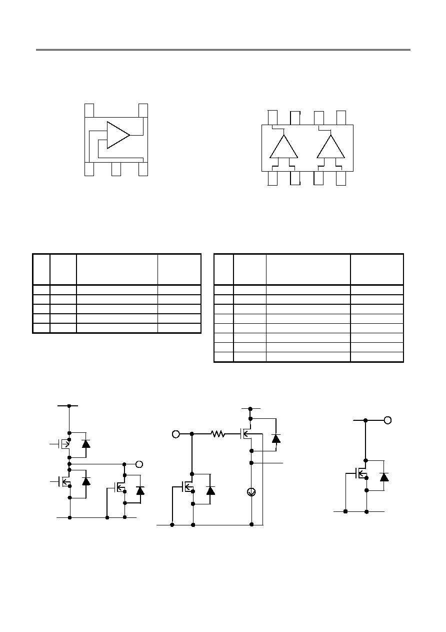
Pin Configuration
(S-8953xACNC)
5-Pin SC-88A
Top View
VSS
IN(
+)
IN(
-)
VDD
OUT
1
2
3
5
4
+
-
-
-
-
Figure 1
Figure 2
[Internal equivalent circuits]
(1) Output pin
(2) Input pin
(3) VDD pin
VDD
VSS
VSS
VDD
VSS
VDD
Figure 3
Figure 4
Figure 5
Table 5 Pin Description (S-8953xBCPN)
Pin
No.
Symbol Description
Internal
Equivalent
Circuit
1 IN1(
-) Inverted input pin 1
Figure 4
2 IN1(
+) Non-inverted input pin 1
Figure 4
3 IN2(
-) Inverted input pin 2
Figure 4
4 IN2(
+) Non-inverted input pin 2
Figure 4
5 VSS
GND
pin
6
OUT2 Output pin 2
Figure 3
7
VDD
Positive power pin
Figure 5
8
OUT1 Output pin 1
Figure 3
Table 4 Pin Description (S-8953xACNC)
Pin
No.
Symbol
Description
Internal
Equivalent
Circuit
1 IN(
+) Non-inverting input pin
Figure 4
2 VSS
GND
pin
3 IN(
-) Inverted input pin
Figure 4
4
OUT Output pin
Figure 3
5
VDD Positive power supply pin
Figure 5
(S-8953xBCPN)
8-Pin SON(A)
Top View
VSS
IN1(
+)
IN1(
-)
IN2(
+)
IN2(
-)
VDD
OUT1
OUT2
1
2
3
5
4
8
7
6
-
+
-
+
MINI ANALOG SERIES 0.7
µA RAIL-TO-RAIL CMOS COMPARATOR
Rev.1.2
_02
S-8953xA/B Series
4
Seiko Instruments Inc.
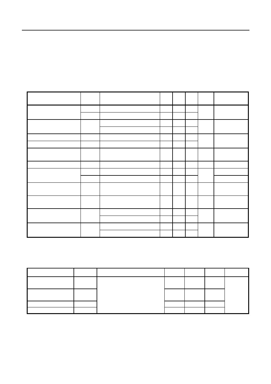
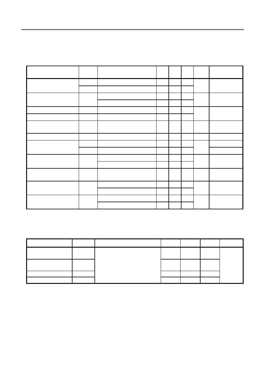
Electrical Characteristics
The S-89530ACNC and S-89531ACNC, and the S-89530BCPN and S-89531BCPN only differ in the input
offset voltage. All other specifications are the same.
1. V
DD
=
=
=
= 3.0 V
DC Characteristics (V
DD
= 3.0 V)
Table 6
(Ta
= 25°C unless otherwise specified)
Parameter
Symbol Conditions Min.
Typ.
Max.
Unit
Measurement
circuit
Supply current
I
DDH
V
IN1
= V
SS
, V
IN2
= V
DD
, R
L
= 0.7 1.4
(per circuit)
I
DDL
V
IN1
= V
DD
, V
IN2
= V
SS
, R
L
= 0.25 0.5
µA Figure
11
S-89530A/B: V
CMR
= 1.5 V
-10 ±5 +10
Input offset voltage
V
IO
S-89531A/B: V
CMR
= 1.5 V
-5
±3
+5
mV Figure
7
Input offset current
I
IO
1
Input bias current
I
BIAS
1
pA
Common-mode input
voltage range
V
CMR
0
3.0 V
Figure
8
Voltage gain (open loop)
A
VOL
V
CMR
= 1.5 V, R
L
= 1 M
86 dB
Maximum output swing
V
OH
R
L
= 1 M
2.98
Figure
9
voltage V
OL
R
L
= 1 M
0.02
V
Figure 10
Common-mode input
signal rejection ratio
CMRR V
SS
V
CMR
V
DD
45
65
dB Figure
8
Power supply voltage
rejection ratio
PSRR V
DD
= 0.9 V to 5.5 V
66
75
dB Figure
6
V
OUT
= V
DD
- 0.1 V
380 500
Source current
*1
I
SOURCE
V
OUT
= 0 V
4000 5500
µA Figure
12
V
OUT
= 0.1 V
400 550
Sink current
I
SINK
V
OUT
= V
DD
4800
6000
µA Figure
13
*1. Be sure to use the product with a source current of no more than 7 mA.
AC Characteristics (V
DD
= 3.0 V)
Table 7
(Ta
= 25°C, unless otherwise specified)
Parameter Symbol
Conditions
Min.
Typ.
Max.
Unit
Rise propagation
delay time
t
PLH
110
Fall propagation
Overdrive
= 100 mV
delay time
t
PHL
C
L
= 15 pF
280
Output rise time
t
TLH
(Refer to Figure 14.)
10
Output fall time
t
THL
30
µs
MINI ANALOG SERIES 0.7
µA RAIL-TO-RAIL CMOS COMPARATOR
S-8953xA/B Series
Rev.1.2
_02
Seiko Instruments Inc.
5
2. V
DD
=
=
=
= 1.8 V
DC Characteristics (V
DD
= 1.8 V)
Table 8
(Ta
= 25°C unless otherwise specified)
Parameter
Symbol Conditions Min.
Typ.
Max.
Unit
Measurement
circuit
Supply current
I
DDH
V
IN1
= V
SS
, V
IN2
= V
DD
, R
L
= 0.7 1.4
(per circuit)
I
DDL
V
IN1
= V
DD
, V
IN2
= V
SS
, R
L
= 0.25 0.5
µA Figure
11
S-89530A/B: V
CMR
= 0.9 V
-10 ±5 +10
Input offset voltage
V
IO
S-89531A/B: V
CMR
= 0.9 V
-5
±3
+5
mV Figure
7
Input offset current
I
IO
1
Input bias current
I
BIAS
1
pA
Common-mode input
voltage range
V
CMR
0
1.8 V
Figure
8
Voltage gain (open loop)
A
VOL
V
CMR
= 0.9 V, R
L
= 1 M
80 dB
Maximum output swing
V
OH
R
L
= 1 M
1.78
Figure
9
voltage V
OL
R
L
= 1 M
0.02
V
Figure 10
Common-mode input
V
SS
V
CMR
V
DD
35
55
signal rejection ratio
CMRR
V
SS
V
CMR
V
DD
- 0.2 V
45
60
dB Figure
8
Power supply voltage
rejection ratio
PSRR V
DD
= 0.9 V to 5.5 V
66
75
dB Figure
6
V
OUT
= V
DD
- 0.1 V
200 250
Source current
I
SOURCE
V
OUT
= 0 V
1000 1500
µA Figure
12
V
OUT
= 0.1 V
220 300
Sink current
I
SINK
V
OUT
= V
DD
1200
1800
µA Figure
13
AC Characteristics (V
DD
= 1.8 V)
Table 9
(Ta
= 25°C unless otherwise specified)
Parameter Symbol
Conditions
Min.
Typ.
Max.
Unit
Rise propagation
delay time
t
PLH
90
Fall propagation
Overdrive
= 100 mV
delay time
t
PHL
C
L
= 15 pF
160
Output rise time
t
TLH
(Refer to Figure 14.)
8
Output fall time
t
THL
25
µs
Document Outline
- S-8953xA/B Series
- COVER
- Features
- Packages
- Selection Guide
- Absolute Maximum Ratings
- Recommended Operating Power Supply Voltage
- Pin Configuration
- Electrical Characteristics
- Measurement Circuits
- Cautions
- Typical Performance Characteristics
- Dimensions
- 5-Pin SC-88A
- 8-Pin SON(A)