S90N0232SUA_E3.0_00

Rev.3.0
_00
N-CHANNEL POWER MOS FET FOR SWITCHING
S-90N0232SUA
Seiko Instruments Inc.
1
The S-90N0232SUA is an N-channel power MOS
FET that realizes a low on-state resistance and ultra
high-speed switching characteristics. It is suitable for
speeding up switching, enabling a high efficient set
and energy saving. A gate protection diode is built in
as a countermeasure for static electricity. Small
SOT-89-3 package realize high-density mounting.
This product can be driven directly by a 2.5 V power
source. If use this product in combination with SII
switching regulator products, you can get the highest
performance.
Features
· Low on-state resistance:
R
DS(on)1
= 0.11
Max. (V
GS
= 4.5 V, I
D
= 1.5 A)
R
DS(on)2
= 0.17
Max. (V
GS
= 2.5 V, I
D
= 1.5 A)
· Ultra high-speed switching
· Operational voltage:
2.5 V drive available
· Built-in gate protection diode
· Small package:
SOT-89-3
Applications
· Notebook PCs
· Cellular and portable phones
· On-board power supplies
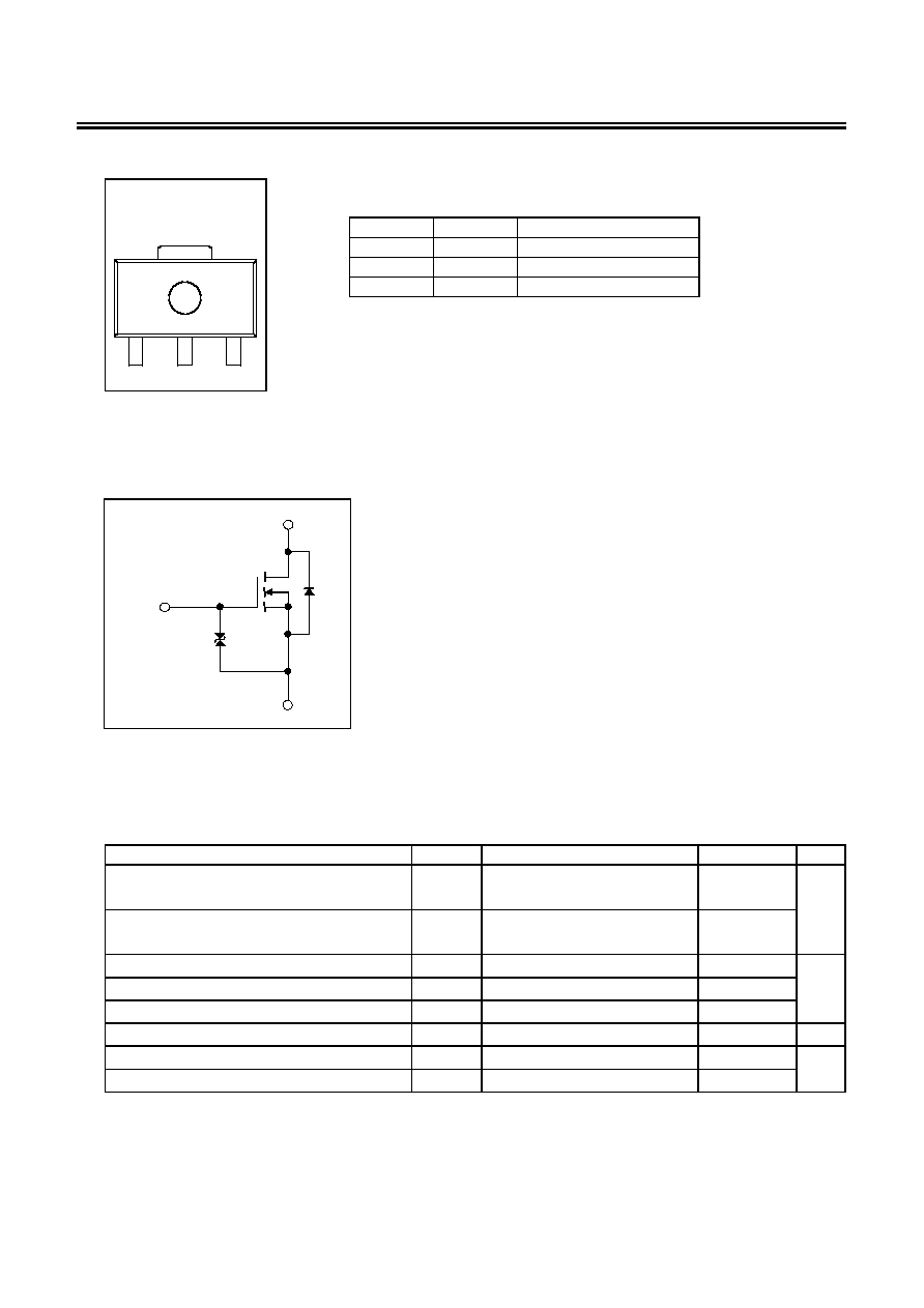
Packages
· SOT-89-3
(Package drawing code: UP003-A)
Item code
· Item code
: S-90N0232SUA-TF
· Delivery form
: Taping only
N-CHANNEL POWER MOS FET FOR SWITCHING
S-90N0232SUA
Rev.3.0
_00
Seiko Instruments Inc.
2
Pin Configuration
Table 1
Pin
No.
Symbol
Description
1
G
Gate
pin
2
D
Drain
pin
3
S
Source
pin
SOT-89-3
Top view
1 2 3
Figure 1
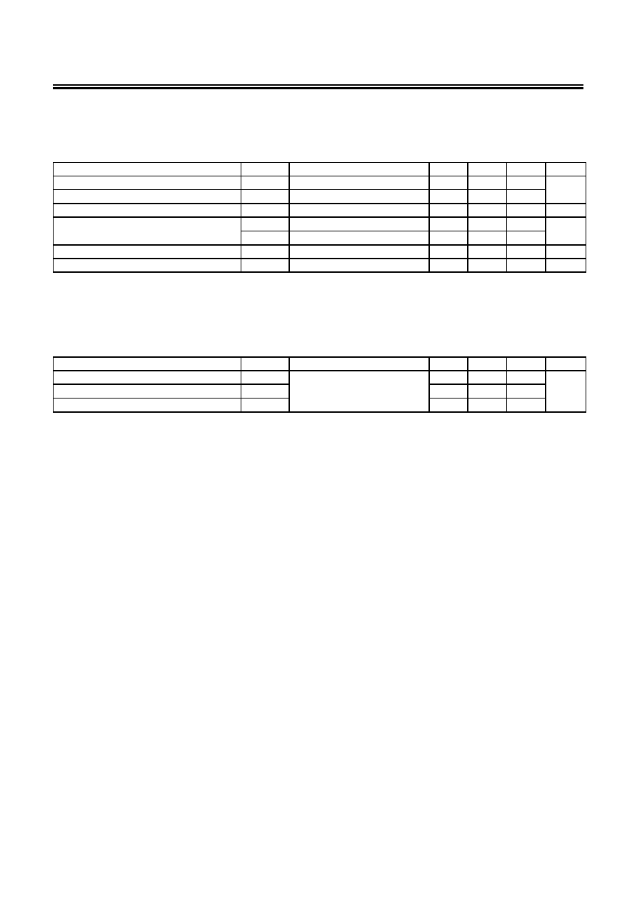
Equivalent Circuit
G (Gate)
D (Drain)
S (Source)
Gate
Protection
Diode
Body
Diode
Caution The diode connected between the gate and source of the
transistor serves as a protector against electrostatic
discharge. Do not apply an electrostatic discharge to this
IC that exceeds the performance ratings of the built-in
gate protection diode.
And when this device actually used, an additional
protection circuit is externally required if a voltage
exceeding the rated voltage may be applied to this
device.
Figure 2
Absolute Maximum Ratings
Table 2
(Ta = 25
°C unless otherwise specified)
Item Symbol
Conditions
Ratings
Unit
Drain to source voltage
(When between gate and source short circuits)
V
DSS
V
GS
= 0 V
20
V
Gate to source voltage
(When between drain and source short circuits)
V
GSS
V
DS
= 0 V
±12
Drain current (DC)
I
D
3
A
Drain current (Pulse)
I
DP
PW = 10
µs, Duty Cycle1%
9
Reverse drain current
I
DR
3
Power dissipation
*1, *2
P
D
2.5
W
Channel temperature
T
ch
150
°C
Storage temperature
T
stg
-55 to +150
Caution The absolute maximum ratings are rated values exceeding which the product could suffer
physical damage. These values must therefore not be exceeded under any conditions.
*1. Mounted on a ceramics board (1225 mm
2
× 1 mm)
*2. The allowable power dissipation differs depending on the mounting form.
N-CHANNEL POWER MOS FET FOR SWITCHING
Rev.3.0
_00
S-90N0232SUA
Seiko Instruments Inc.
3
Electrical Characteristics
DC characteristics
Table 3
(Ta = 25
°C unless otherwise specified)
Item
Symbol Conditions
Min. Typ. Max.
Unit
Drain cut-off current
I
DSS
V
DS
= 20 V, V
GS
= 0 V
10
µA
Gate to source leakage current
I
GSS
V
GS
= ±12 V, V
DS
= 0 V
±10
Gate to source cut-off voltage
V
GS(off)
I
D
= 1 mA, V
DS
= 10 V
0.7
1.4 V
Drain to source on-state resistance
*1
R
DS(on)1
I
D
= 1.5 A, V
GS
= 4.5 V
0.08 0.11
R
DS(on)2
I
D
= 1.5 A, V
GS
= 2.5 V
0.13 0.17
Forward transfer admittance
*1
|Y
fs
| I
D
= 1.5 A, V
DS
= 10 V
6
S
Body drain diode forward voltage
V
f
I
f
= 3 A, V
GS
= 0 V
0.85 1.1 V
*1. Effective during pulse test (600
µs).
Dynamic characteristics
Table 4
(Ta = 25
°C unless otherwise specified)
Item
Symbol Conditions
Min. Typ. Max.
Unit
Input capacitance
C
iss
V
DS
= 10 V, V
GS
= 0 V,
185
pF
Output capacitance
C
oss
f = 1 MHz
65
Feedback capacitance
C
rss
45
N-CHANNEL POWER MOS FET FOR SWITCHING
S-90N0232SUA
Rev.3.0
_00
Seiko Instruments Inc.
4
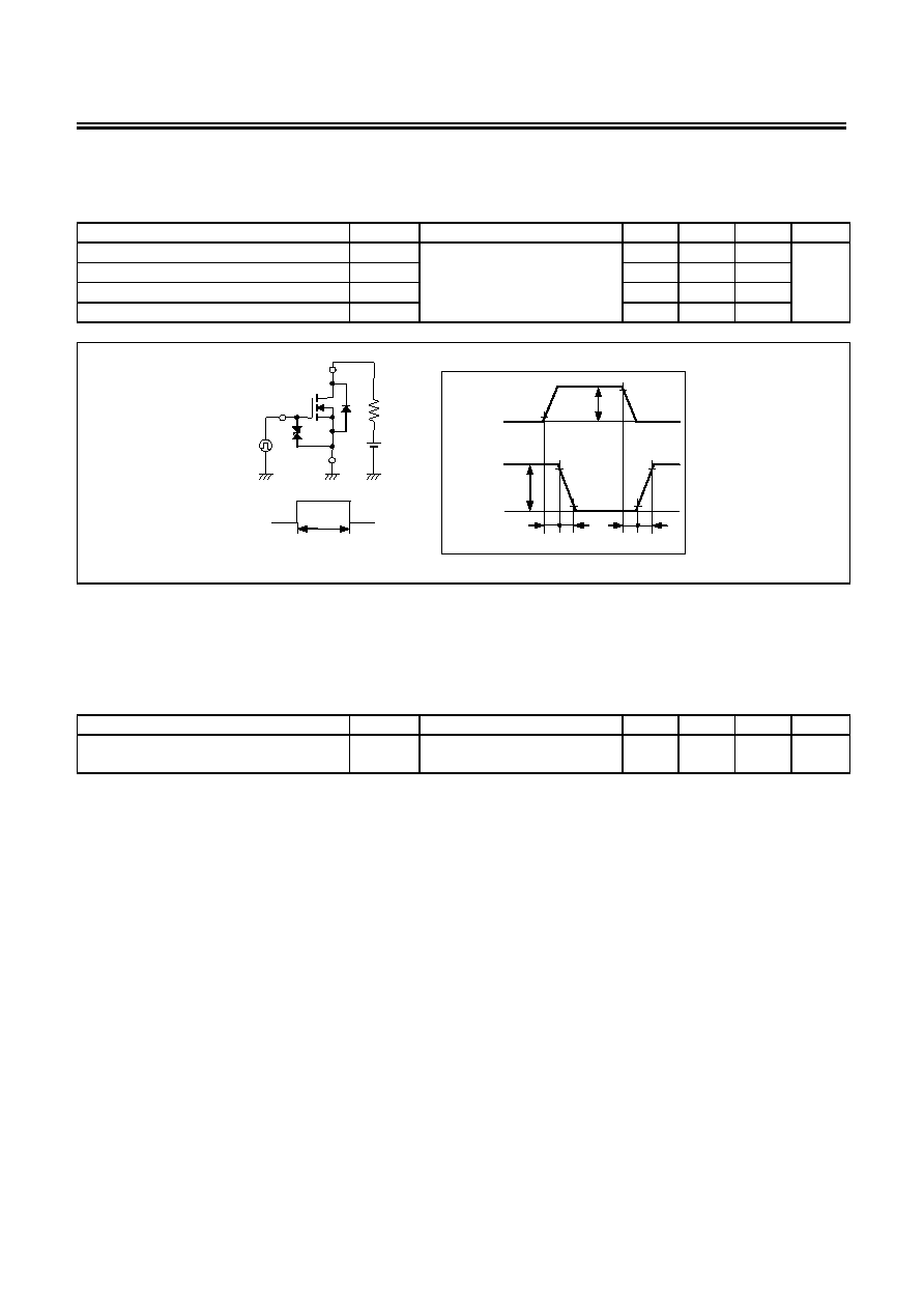
Switching characteristics
Table 5
(Ta = 25
°C unless otherwise specified)
Item
Symbol Conditions
Min. Typ. Max.
Unit
Turn-on delay time
t
d(on)
V
GS
= 5 V, I
D
= 1.5 A,
10
ns
Rise time
t
r
V
DD
= 10 V
35
Turn-off delay time
t
d(off)
45
Fall time
t
f
30
D.U.T.
R
L
V
DD
PG.
V
GS
0
= 10 µs
Duty Cycle
1 %
10 %
90 %
10 %
90 %
t
d(on)
t
d(off)
t
r
t
f
V
DS
V
GS
V
DS
Wave Form
V
GS
Wave Form
0
0
10 %
90 %
Figure 3
Thermal characteristics
Table 6
(Ta = 25
°C unless otherwise specified)
Item
Symbol Conditions
Min. Typ. Max.
Unit
Thermal resistance
(Channel to ambience)
R
th(ch-a)
Mounted on a ceramics board
(1225 mm
2
× 1 mm)
50 °C/W
Precautions
· The application conditions for the input voltage, output voltage, and load current should not exceed the
allowable package power dissipation after mounting.
· SII claims no responsibility for any disputes arising out of or in connection with any infringement by
products including this IC of patents owned by a third party.
N-CHANNEL POWER MOS FET FOR SWITCHING
Rev.3.0
_00
S-90N0232SUA
Seiko Instruments Inc.
5
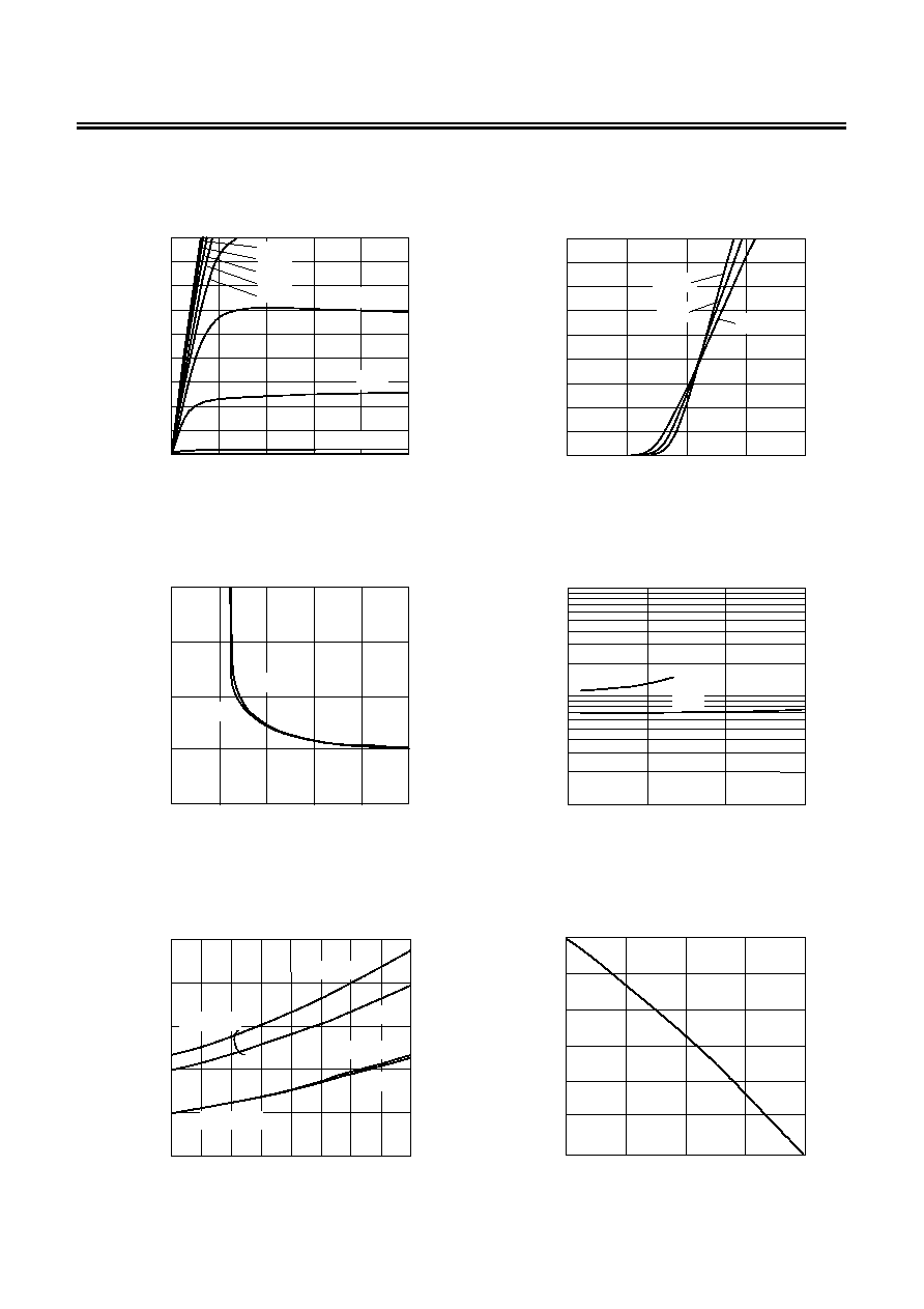
Typical Characteristics
DRAIN CURRENT vs. DRAIN TO SOURCE VOLTAGE
DRAIN CURRENT vs. GATE TO SOURCE VOLTAGE
Pulse test (600
µs), Ta = 25°C
Pulse test (600
µs), V
DS
= 10 V
Drai
n Current
I
D
[A]
9
8
7
6
5
4
3
2
1
0
2
3
5.0 V
4.5 V
4.0 V
3.5 V
3.0 V
V
GS
= 2.5 V
0
1
4
5
2.0 V
1.5 V
Drai
n Current
I
D
[A]
9
8
7
6
5
4
3
2
1
0
2
3
1
4
0
125 °C
25 °C
55 °C
Drain to Source Voltage V
DS
[V]
Gate to Source Voltage V
GS
[V]
DRAIN TO SOURCE ON-STATE RESISTANCE
vs. GATE TO SOURCE VOLTAGE
DRAIN TO SOURCE ON-STATE RESISTANCE
vs. DRAIN CURRENT
Pulse test (600
µs), Ta = 25°C
Pulse test (600
µs), Ta = 25°C
Drai
n t
o
S
ourc
e
On-S
t
a
t
e
Res
i
s
t
anc
e
R
D
S
(
on)
[
]
0.2
0.15
0.1
0.05
0
4
6
2
8
3.0 A
I
D
= 1.5 A
0
10
Drai
n t
o
S
ourc
e
On-S
t
a
t
e
Res
i
s
t
anc
e
R
D
S
(
on)
[
]
1
0.1
0.01
6
9
3
0
V
GS
= 2.5 V
4.5 V
Gate to Source Voltage V
GS
[V]
Drain Current I
D
[A]
DRAIN TO SOURCE ON-STATE RESISTANCE
vs. AMBIENT TEMPERATURE
GATE TO SOURCE CUT-OFF VOLTAGE VARIANCE
vs. AMBIENT TEMPERATURE
Pulse test (600
µs)
V
DS
= 10 V, I
D
= 1 mA
Drai
n t
o
S
ourc
e
On-S
t
a
t
e
Res
i
s
t
anc
e
R
D
S
(
on)
[
]
0.25
0.20
0.15
0.10
0.05
0
V
GS
= 4.5 V
25
25
75
100
50
0
50
125
150
V
GS
= 2.5 V
I
D
= 3.0 A
1.5 A
I
D
= 3.0 A
1.5 A
Gat
e
t
o
S
ourc
e
Cut
-
of
f
V
o
l
t
age V
a
ri
anc
e
V
G
S
(
o
ff)
V
a
ri
anc
e [
V
]
0.2
0.1
0
0.1
0.2
0.3
0.4
100
50
0
50
150
Ambient Temperature Ta [°C]
Ambient Temperature Ta [°C]
Document Outline
- S-90N0232SUA
- Cover
- Features
- Applications
- Packages
- Item code
- Pin Configuration
- Equivalent Circuit
- Absolute Maximum Ratings
- Electrical Characteristics
- Precautions
- Typical Characteristics
- Marking Specification
- Package drawing