Rev. 2.1
_00
CMOS SERIAL E
2
PROM
S-93C46B/56B/66B
Seiko Instruments Inc.
1
The S-93C46B/56B/66B is a high speed, low current
consumption, 1/2/4 K-bit serial E
2
PROM with a wide
operating voltage range. It is organized as 64-word
◊ 16-bit, 128-word ◊ 16-bit, 256-word ◊ 16-bit,
respectively. Each is capable of sequential read, at
which time addresses are automatically incremented
in 16-bit blocks. The instruction code is compatible
with the NM93CS46/56/66.
Features
∑ Low current consumption
Standby:
1.5
µA Max. (V
CC
= 5.5 V)
Operating: 0.8 mA Max. (V
CC
= 5.5 V)
0.4 mA Max. (V
CC
= 2.5 V)
∑ Wide operating voltage range Read:
1.8 to 5.5 V (at
-40 to +85∞C)
Write:
2.7 to 5.5 V (at
-40 to +85∞C)
∑ Sequential read capable
∑ Write disable function when power supply voltage is low
∑ Function to protect against write due to erroneous instruction recognition
∑ Endurance:
10
7
cycles/word (at
+25∞C) write capable,
10
6
cycles/word (at
+85∞C),
3
◊ 10
5
cycles/word (at
+105∞C)
∑ Data retention: 10 years (after rewriting 10
6
cycles/word at
+85∞C)
∑ S-93C46B:
1 K-bit NM93CS46 instruction code compatible
∑ S-93C56B:
2 K-bit NM93CS56 instruction code compatible
∑ S-93C66B:
4 K-bit NM93CS66 instruction code compatible
∑ High-temperature operation: +105∞C Max. supported
(Only S-93C46BD0H-J8T2, S-93C56BD0H-J8T2 and S-93C66BD0H-J8T2)
Packages
Package name
Drawing code
Package
Tape Reel
8-Pin DIP
DP008-F
8-Pin SOP(JEDEC)
FJ008-A
FJ008-D
FJ008-D
8-Pin TSSOP
FT008-A
FT008-D
FT008-D
Caution This product is intended to use in general electronic devices such as consumer electronics,
office equipment, and communications devices. Before using the product in medical
equipment or automobile equipment including car audio, keyless entry and engine control
unit, contact to SII is indispensable.
CMOS SERIAL E
2
PROM
S-93C46B/56B/66B
Rev.2.1
_00
Seiko Instruments Inc.
2
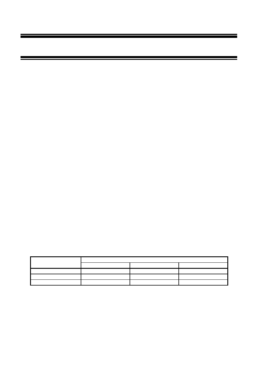
Pin Assignment
8-Pin DIP
Top view
Table 1
Pin Number
Pin Name
Function
1 CS
Chip select input
2 SK
Serial clock input
3 DI
Serial data input
4 DO
Serial data output
5 GND
Ground
6
TEST
*1
Test
7 NC
No
connection
8 VCC
Power
supply
*1. Connect to GND or V
CC
.
1
2
3
4
8
7
6
5
VCC
NC
TEST
GND
CS
SK
DO
DI
Figure 1
S-93C46BD0I-D8S1
S-93C56BD0I-D8S1
S-93C66BD0I-D8S1
Remark See Dimensions for details of the package drawings.
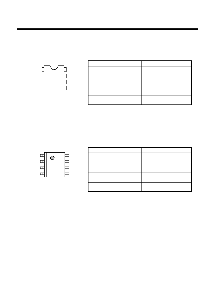
8-Pin SOP(JEDEC)
Top view
Table 2
Pin Number
Pin Name
Function
1 CS
Chip select input
2 SK
Serial clock input
3 DI
Serial data input
4 DO
Serial data output
5 GND
Ground
6
TEST
*1
Test
7 NC
No
connection
8 VCC
Power
supply
*1. Connect to GND or V
CC
.
1
2
3
4
8
7
6
5
VCC
NC
TEST
GND
CS
SK
DO
DI
Figure 2
S-93C46BD0I-J8T1
S-93C46BD0H-J8T2
S-93C56BD0I-J8T1
S-93C56BD0H-J8T2
S-93C66BD0I-J8T1
S-93C66BD0H-J8T2
Remark See Dimensions for details of the package drawings.

CMOS SERIAL E
2
PROM
Rev.2.1
_00
S-93C46B/56B/66B
Seiko Instruments Inc.
3
8-Pin SOP(JEDEC) (Rotated)
Top view
Table 3
Pin Number
Pin Name
Function
1 NC
No
connection
2 VCC
Power
supply
3 CS
Chip select input
4 SK
Serial clock input
5 DI
Serial data input
6 DO
Serial data output
7 GND
Ground
8
TEST
*1
Test
*1. Connect to GND or V
CC
.
1
2
3
4
8
7
6
5
CS
SK
TEST
GND
DO
DI
VCC
NC
Figure 3
S-93C46BR0I-J8T1
S-93C56BR0I-J8T1
S-93C66BR0I-J8T1
Remark See Dimensions for details of the package drawings.
8-Pin TSSOP
Top view
Table 4
Pin Number
Pin Name
Function
1 CS
Chip select input
2 SK
Serial clock input
3 DI
Serial data input
4 DO
Serial data output
5 GND
Ground
6
TEST
*1
Test
7 NC
No
connection
8 VCC
Power
supply
*1. Connect to GND or V
CC
.
1
2
3
4
8
7
6
5
VCC
NC
TEST
GND
CS
SK
DO
DI
Figure 4
S-93C46BD0I-T8T1
S-93C56BD0I-T8T1
S-93C66BD0I-T8T1
Remark See Dimensions for details of the package drawings.
CMOS SERIAL E
2
PROM
S-93C46B/56B/66B
Rev.2.1
_00
Seiko Instruments Inc.
4
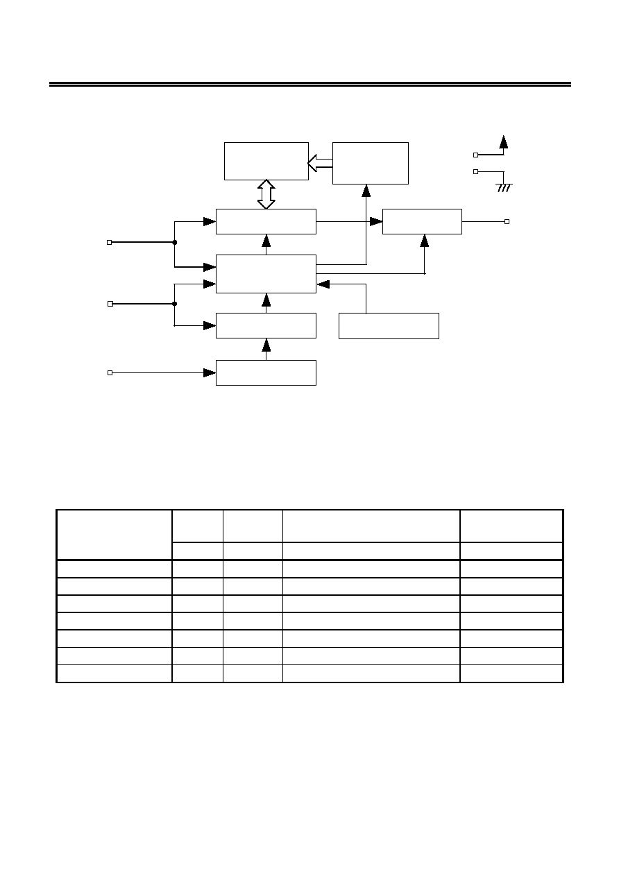
Block Diagram
Memory array
Data register
Address
decoder
Mode decode logic
Clock pulse
monitoring circuit
Output buffer
VCC
GND
DO
DI
CS
Clock generator
Voltage detector
SK
Figure 5
Instruction Sets
1. S-93C46B
Table 5
Instruction Start
Bit
Operation
Code
Address Data
SK
input
clock 1 2 3 4 5 6 7 8 9
10
to
25
READ (Read data)
1
1
0
A5 A4 A3 A2 A1 A0 D15 to D0
Output
*1
WRITE (Write data)
1
0
1
A5 A4 A3 A2 A1 A0 D15 to D0 Input
ERASE (Erase data)
1
1
1
A5 A4 A3 A2 A1 A0
WRAL (Write all)
1
0
0
0
1
x x x x
D15 to D0 Input
ERAL (Erase all)
1
0
0
1
0
x x x x
EWEN (Write enable)
1
0
0
1
1
x x x x
EWDS (Write disable)
1
0
0
0
0
x x x x
Remark x: Doesn't matter
*1. When the 16-bit data in the specified address has been output, the data in the next address is output.
CMOS SERIAL E
2
PROM
Rev.2.1
_00
S-93C46B/56B/66B
Seiko Instruments Inc.
5
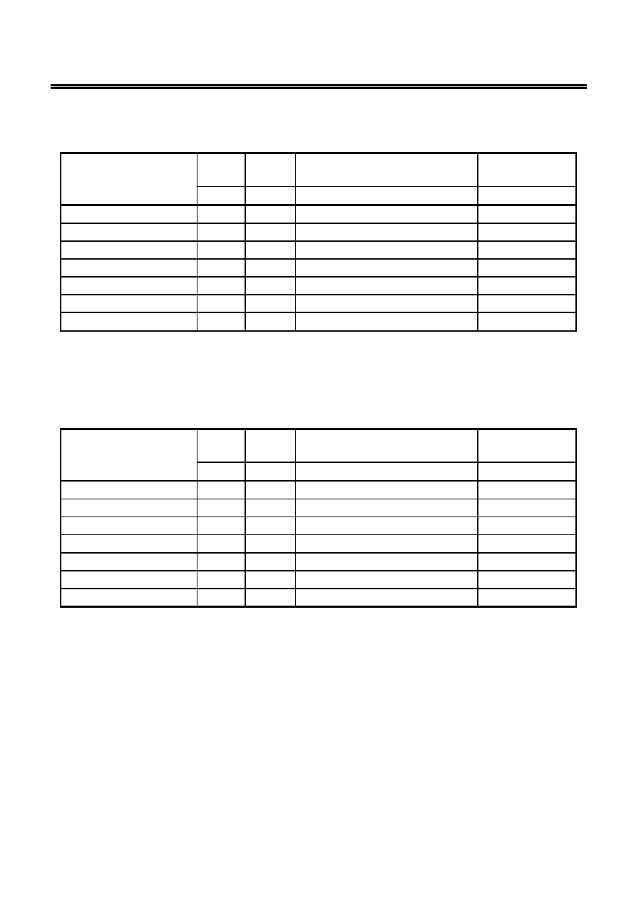
2. S-93C56B
Table 6
Instruction Start
Bit
Operation
Code
Address Data
SK
input
clock 1
2 3 4 5 6 7 8 9 10 11
12
to
27
READ (Read data)
1
1
0
x A6 A5 A4 A3 A2 A1 A0 D15 to D0
Output
*1
WRITE (Write data)
1
0
1
x A6 A5 A4 A3 A2 A1 A0 D15 to D0 Input
ERASE (Erase data)
1
1
1
x A6 A5 A4 A3 A2 A1 A0
WRAL (Write all)
1
0
0
0
1
x x x x x x D15 to D0 Input
ERAL (Erase all)
1
0
0
1
0
x x x x x x
EWEN (Write enable)
1
0
0
1
1
x x x x x x
EWDS (Write disable)
1
0
0
0
0
x x x x x x
Remark x: Doesn't matter
*1. When the 16-bit data in the specified address has been output, the data in the next address is output.
3. S-93C66B
Table 7
Instruction Start
Bit
Operation
Code
Address Data
SK
input
clock 1
2 3 4 5 6 7 8 9 10 11
12
to
27
READ (Read data)
1
1
0
A7 A6 A5 A4 A3 A2 A1 A0 D15 to D0
Output
*1
WRITE (Write data)
1
0
1
A7 A6 A5 A4 A3 A2 A1 A0 D15 to D0 Input
ERASE (Erase data)
1
1
1
A7 A6 A5 A4 A3 A2 A1 A0
WRAL (Write all)
1
0
0
0
1
x x x x x x D15 to D0 Input
ERAL (Erase all)
1
0
0
1
0
x x x x x x
EWEN (Write enable)
1
0
0
1
1
x x x x x x
EWDS (Write disable)
1
0
0
0
0
x x x x x x
Remark x: Doesn't matter
*1. When the 16-bit data in the specified address has been output, the data in the next address is output.