Contents
Features .............................................................. 1
Pin Assignment ................................................... 1
Pin Functions ...................................................... 1
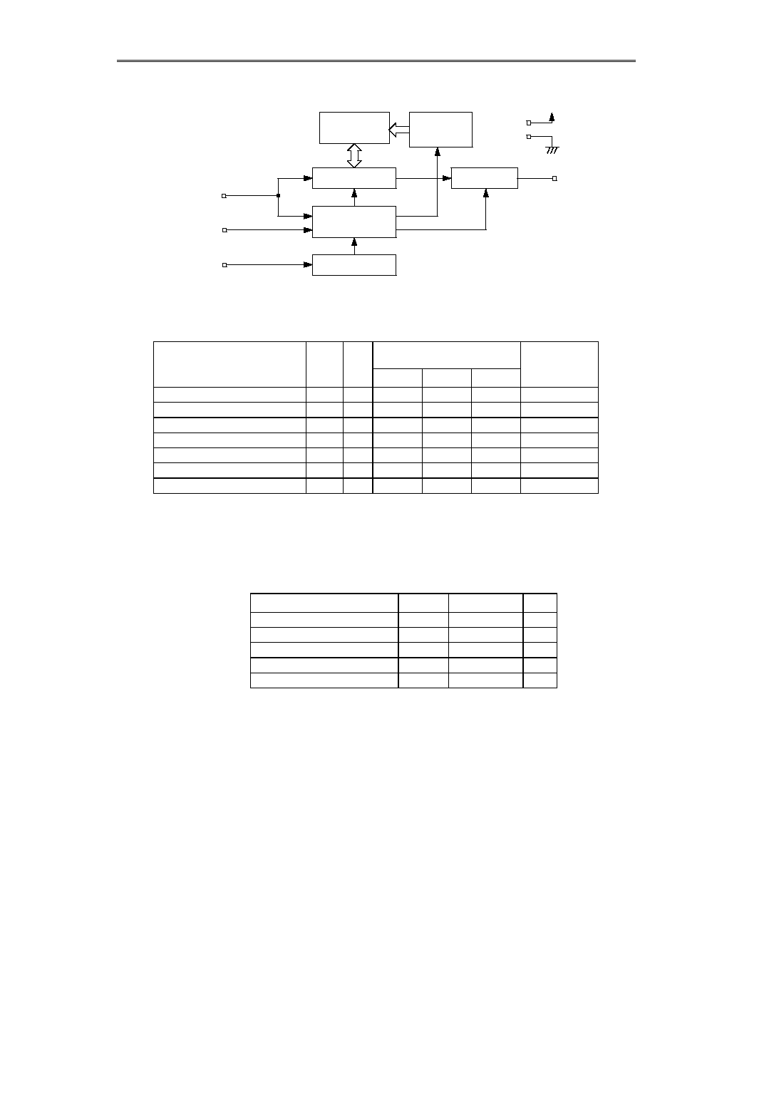
Block Diagram ..................................................... 2
Instruction Set ..................................................... 2
Absolute Maximum Ratings................................. 2
Recommended Operating Conditions ................. 3
Pin Capacitance .................................................. 3
Endurance........................................................... 3
DC Electrical Characteristics ............................... 4
AC Electrical Characteristics ............................... 5
Operation ............................................................ 6
Receiving a Start-Bit............................................ 13
Three-wire Interface (DI-DO direct connection) ... 13
Dimensions (Unit : mm) ....................................... 14
Ordering Information ........................................... 17
Characteristics..................................................... 18
Frequently Asked Questions................................ 23
Seiko Instruments Inc.
1
The S-93C46A/56A/66A is high speed, low power 1K/2K/4K-bit E
2
PROM
with a wide operating voltage range. It is organized as 64-word
◊
16-bit, 128-
word
◊
16-bit, 256-word
◊
16-bit, respectivly. Each is capable of sequential
read, at which time addresses are automatically incremented in 16-bit blocks.
The instruction code is compatible with the NM93CS46/56/66.
n
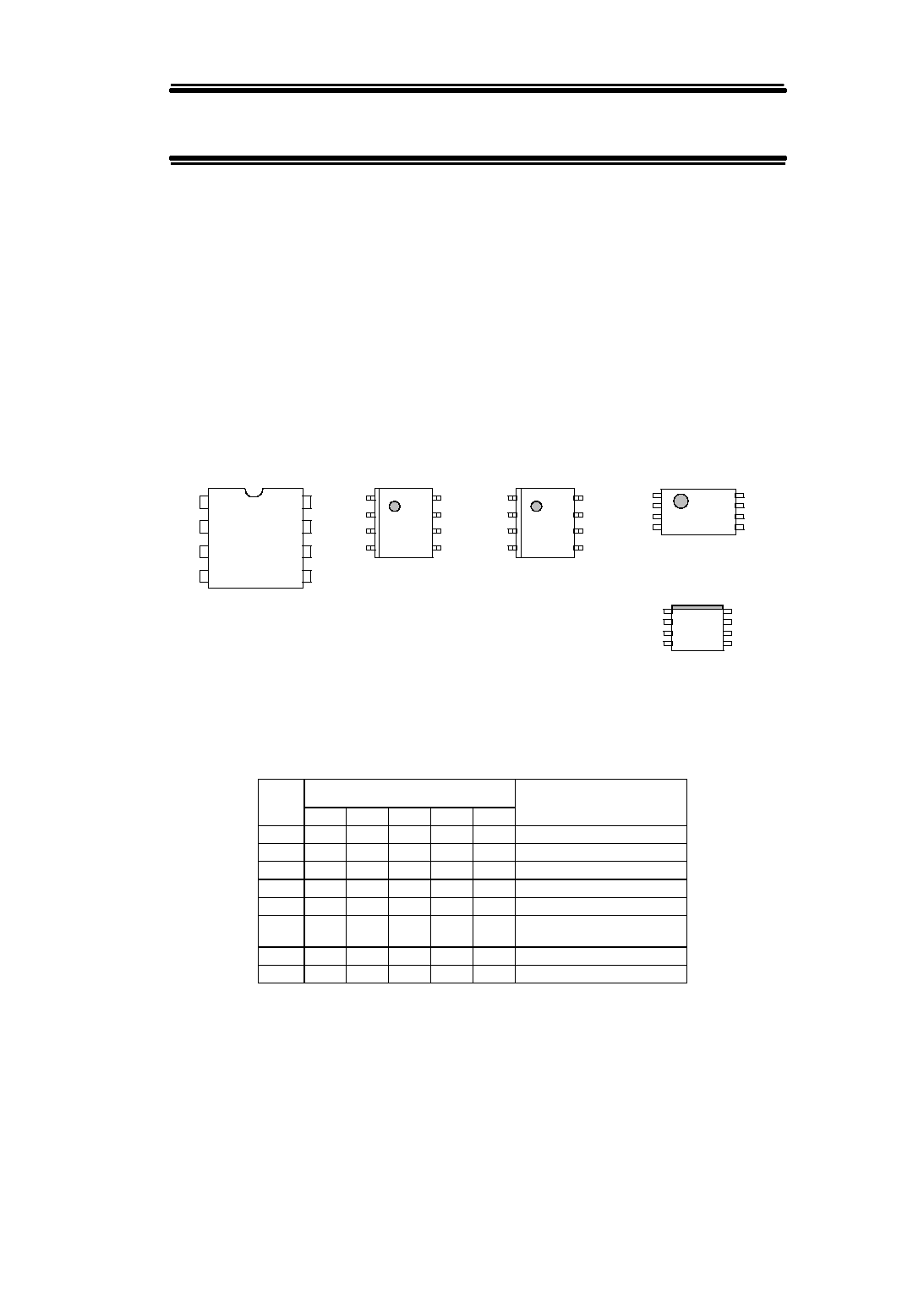
Pin Assignment
n
Pin Functions
Table 1
Name
Pin Number
Function
DIP
SOP1
SOP2
TSSOP MSOP
CS
1
3
1
1
8
Chip select input
SK
2
4
2
2
7
Serial clock input
DI
3
5
3
3
6
Serial data input
DO
4
6
4
4
5
Serial data output
GND
5
7
5
5
4
Ground
TEST
6
8
6
6
3
Test pin (normally kept open)
(can be connected to GND or Vcc)
NC
7
1
7
7
2
No Connection
V
CC
8
2
8
8
1
Power supply
Figure 1
CMOS SERIAL E
2
PROM
S-93C46A/56A/66A
n
Features
Y
Low power consumption
Standby
: 1.0
µ
A Max.
(VCC=5.5 V)
Operating : 0.8 mA Max. (VCC=5.5 V)
: 0.4 mA Max. (VCC=2.5 V)
Y
Wide operating voltage range
Read/Write : 1.8 to 5.5 V
Y
Sequential read capable
Y
Endurance : 10
6
cycles/word
Y
Data retention : 10 years
Y
S-93C46A : 1K bits NM93CS46 instruction code compatible
Y
S-93C56A : 2K bits NM93CS56 instruction code compatible
Y
S-93C66A : 4K bits NM93CS66 instruction code compatible
8-pin DIP
Top view
V
CC
DO
NC
TEST
SK
DI
GND
CS
1
2
3
4
5
6
7
8
S-93C46ADP
S-93C56ADP
S-93C66ADP
8-pin TSSOP
Top view
1
2
3
4
8
7
6
5
CS
SK
DI
DO
V
CC
NC
TEST
GND
S-93C46AFT
S-93C56AFT
S-93C66AFT
* See
n
Dimensions
S-93C46AMFN
S-93C56AMFN
S-93C66AMFN
8-pin MSOP
Top view
1
2
3
4
8
7
6
5
V
CC
NC
TEST
GND
CS
SK
DI
DO
S-93C46AFJ
S-93C56AFJ
S-93C66AFJ
8-pin SOP1
Top view
NC
GND
TEST
DO
DI
SK
6
5
8
7
3
4
1
2
V
CC
CS
SK
CS
8-pin SOP2
Top view
V
CC
TEST
GND
DI
DO
6
5
8
7
3
4
1
2
NC
S-93C46ADFJ
S-93C56ADFJ
S-93C66ADFJ