Document Outline
- S-93C76A
- Cover
- Features
- Packages
- Pin Assignment
- Block Diagram
- Instruction Sets
- Absolute Maximum Ratings
- Recommended Operating Conditions
- Pin Capacitance
- Endurance
- DC Electrical Characteristics
- AC Electrical Characteristics
- Operation
- Start Bit
- 3-Wire Interface (Direct Connection Between DI and DO)
- Write Disable Function When Power Supply Voltage Is Low
- Precaution
- Characteristics
- Product Code Structure
- Package Drowings
- 8-Pin DIP
- 8-Pin SOP(JEDEC)
- 8-Pin TSSOP

Rev. 2.0
_00
CMOS SERIAL E
2
PROM
S-93C76A
Seiko Instruments Inc.
1
The S-93C76A is a high speed, low current
consumption, 8 K-bit serial E
2
PROM with a wide
operating voltage range. It is organized as 512-word
◊ 16-bit respectively. Each is capable of sequential
read, at which time addresses are automatically
incremented in 16-bit blocks.
Features
∑ Low current consumption
Standby:
2.0
µA Max. (V
CC
= 5.5 V)
Operating: 0.8 mA Max. (V
CC
= 5.5 V)
0.4 mA Max. (V
CC
= 2.5 V)
∑ Wide operating voltage range Read:
1.8 to 5.5 V (at
-40 to +85∞C)
Write:
2.7 to 5.5 V (at
-40 to +85∞C)
∑ Sequential read capable
∑ Write disable function when power supply voltage is low
∑ Endurance:
10
7
cycles/word (at
+25∞C) write capable,
10
6
cycles/word (at
+85∞C),
3
◊ 10
5
cycles/word (at
+105∞C)
∑ Data retention: 10 years (after rewriting 10
6
cycles/word at
+85∞C)
∑ S-93C76A:
8 K-bit
∑ High-temperature operation : +105∞C Max. supported
(Only
S-93C76ADFJ-TBH)
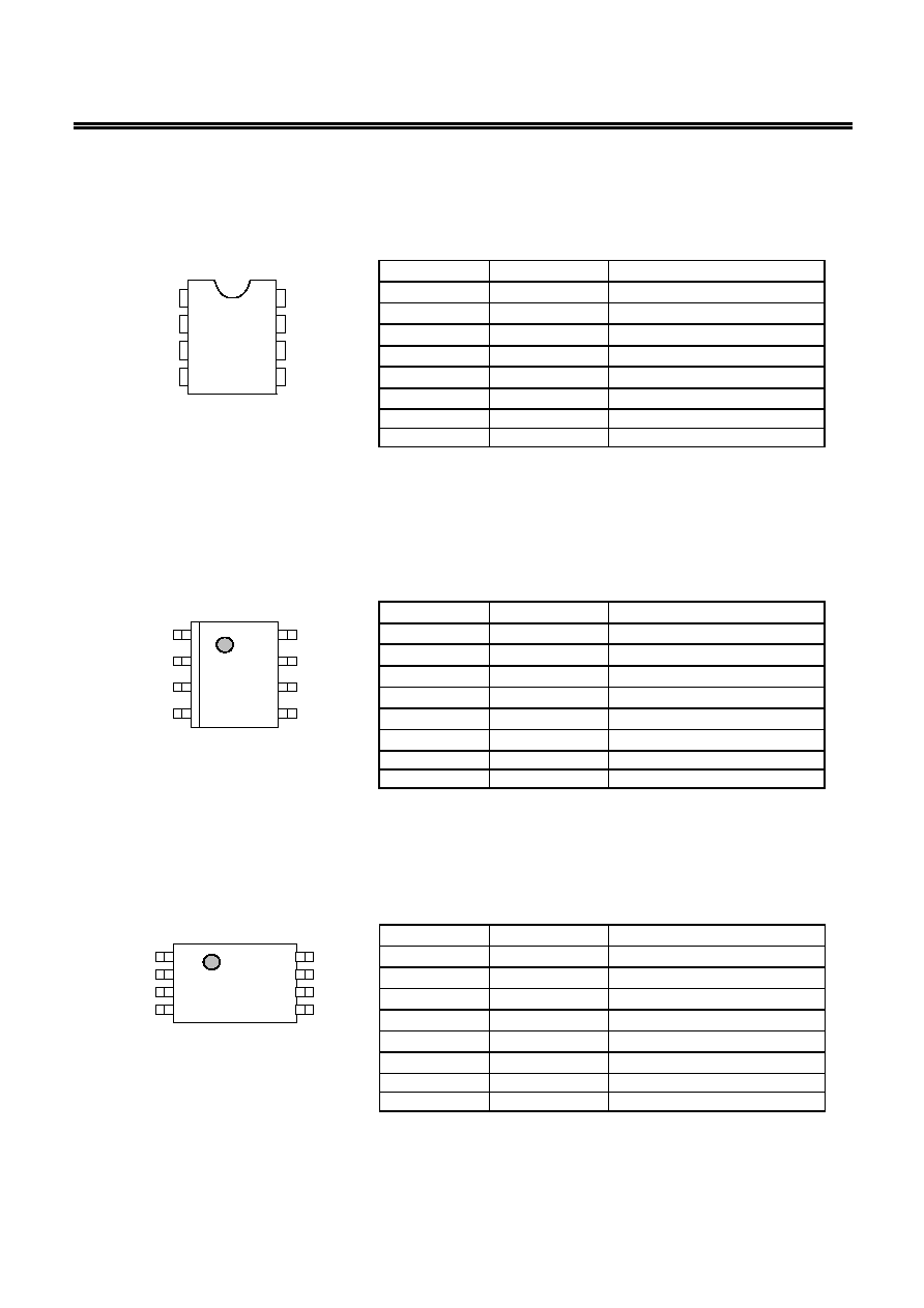
Packages
Package name
Drawing code
Package
Tape Reel
8-Pin DIP
DP008-F
8-Pin SOP(JEDEC)
FJ008-A
FJ008-D
FJ008-D
8-Pin TSSOP
FT008-A
FT008-D
FT008-D
Remark Please refer to the Application Note "TIPS, TRICKS AND TRAPS WHEN USING THE S-29
SERIES AND S-93CxxA SERIES" for equivalent circuit of each pin.
Caution This product is intended to use in general electronic devices such as consumer electronics,
office equipment, and communications devices. Before using the product in medical
equipment or automobile equipment including car audio, keyless entry and engine control
unit, contact to SII is indispensable.
CMOS SERIAL E
2
PROM
S-93C76A
Rev.2.0
_00
Seiko Instruments Inc.
2
Pin Assignment
8-Pin DIP
Top view
Table 1
Pin Number
Pin Name
Function
1 CS
Chip select input
2 SK
Serial clock input
3 DI
Serial data input
4 DO
Serial data output
5 GND
Ground
6
TEST
*1
Test
7 NC
No
connection
8 VCC
Power
supply
*1. Connect to GND or V
CC
.
1
2
3
4
8
7
6
5
VCC
NC
TEST
GND
CS
SK
DO
DI
Figure 1
S-93C76ADP
Remark See Dimensions for details of the package drawings.
8-Pin SOP(JEDEC)
Top view
Table 2
Pin Number
Pin Name
Function
1 CS
Chip select input
2 SK
Serial clock input
3 DI
Serial data input
4 DO
Serial data output
5 GND
Ground
6
TEST
*1
Test
7 NC
No
connection
8 VCC
Power
supply
*1. Connect to GND or V
CC
.
1
2
3
4
8
7
6
5
VCC
NC
TEST
GND
CS
SK
DO
DI
Figure 2
S-93C76ADFJ
Remark See Dimensions for details of the package drawings.
8-Pin TSSOP
Top view
Table 3
Pin Number
Pin Name
Function
1 CS
Chip select input
2 SK
Serial clock input
3 DI
Serial data input
4 DO
Serial data output
5 GND
Ground
6
TEST
*1
Test
7 NC
No
connection
8 VCC
Power
supply
*1. Connect to GND or V
CC
.
1
2
3
4
8
7
6
5
VCC
NC
TEST
GND
CS
SK
DO
DI
Figure 3
S-93C76AFT
Remark See Dimensions for details of the package drawings.

CMOS SERIAL E
2
PROM
Rev.2.0
_00
S-93C76A
Seiko Instruments Inc.
3
Block Diagram
Memory array
Data register
Address
decoder
Mode decode logic
Output buffer
VCC
GND
DO
DI
CS
Clock generator
SK
Figure 4
Instruction Sets
Table 4
Instruction
Start Bit Operation Code
Address
Data
SK input clock
1
2
3
4
5
6
7
8
9 10 11 12 13
14 to 29
READ
(Read
data)
1
1
0
x A8 A7 A6 A5 A4 A3 A2 A1 A0 D15
to
D0
Output
*1
WRITE (Write data)
*2
1
0
1
x A8 A7 A6 A5 A4 A3 A2 A1 A0 D15
to
D0
Input
ERASE (Erase data)
*2
1
1
1
x A8 A7 A6 A5 A4 A3 A2 A1 A0
WRAL (Write all)
*2
1
0
0 0 1 x x x x x x x x
D15
to
D0
Input
ERAL (Erase all)
*2
1
0
0 1 0 x x x x x x x x
EWEN (Write enable)
*2
1
0
0 1 1 x x x x x x x x
EWDS
(Write
disable)
1
0
0 0 0 x x x x x x x x
Remark x: Doesn't matter
*1. When the 16-bit data in the specified address has been output, the data in the next address is output.
*2. WRITE, ERASE, WRAL, ERAL, and EWEN are guaranteed only at V
CC
2.7 V.

CMOS SERIAL E
2
PROM
S-93C76A
Rev.2.0
_00
Seiko Instruments Inc.
4
Absolute Maximum Ratings
Table 5
Parameter Symbol Ratings
Unit
Power supply voltage
V
CC
-0.3 to +7.0 V
Input voltage
V
IN
-0.3 to V
CC
+0.3 V
Output voltage
V
OUT
-0.3 to V
CC
V
Storage temperature
T
stg
-65 to +150
∞C
Caution The absolute maximum ratings are rated values exceeding which the product could suffer
physical damage. These values must therefore not be exceeded under any conditions.
Recommended Operating Conditions
Table 6
-40 to +85∞C
-40 to +105∞C
Parameter Symbol Conditions
Min. Typ. Max. Min.
Typ.
Max.
Unit
READ/EWDS 1.8
5.5 V
Power supply voltage
V
CC
WRITE/ERASE/
WRAL/ERAL/EWEN
2.7
5.5
4.5
5.5
V
V
CC
= 4.5 to 5.5 V
2.0
V
CC
2.0
V
CC
V
V
CC
= 2.7 to 4.5 V
0.8
◊ V
CC
V
CC
V
High level input voltage
V
IH
V
CC
= 1.8 to 2.7 V
0.8
◊ V
CC
V
CC
V
V
CC
= 4.5 to 5.5 V
0.0
0.8 0.0
0.8 V
V
CC
= 2.7 to 4.5 V
0.0
0.2
◊ V
CC
V
Low level input voltage
V
IL
V
CC
= 1.8 to 2.7 V
0.0
0.15
◊ V
CC
V
Operating temperature
T
opr
-40
+85
-40
+105 ∞C
Pin Capacitance
Table 7
(Ta
= 25∞C, f = 1.0 MHz, V
CC
= 5.0 V)
Parameter Symbol
Conditions
Min.
Typ.
Max.
Unit
Input Capacitance
C
IN
V
IN
= 0 V
8
pF
Output Capacitance
C
OUT
V
OUT
= 0 V
10 pF
Endurance
Table 8
Parameter Symbol
Operating
Temperature
Min.
Typ.
Max. Unit
-40 to +85∞C
10
6
Endurance N
W
-40 to +105∞C 3
◊
10
5
cycles/word

CMOS SERIAL E
2
PROM
Rev.2.0
_00
S-93C76A
Seiko Instruments Inc.
5
DC Electrical Characteristics
Table 9
-40 to +85∞C
-40 to +105∞C
V
CC
= 4.5 to 5.5 V V
CC
= 2.5 to 4.5 V V
CC
= 1.8 to 2.5 V V
CC
= 4.5 to 5.5 V
Parameter
Symbol Conditions
Min. Typ. Max. Min. Typ. Max. Min. Typ. Max. Min. Typ. Max.
Unit
Current consumption (READ)
I
CC1
DO no load
0.8 0.5 0.4 0.8 mA
Table 10
-40 to +85∞C
-40 to +105∞C
V
CC
= 4.5 to 5.5 V V
CC
= 2.7 to 4.5 V V
CC
= 4.5 to 5.5 V
Parameter
Symbol Conditions
Min. Typ. Max. Min. Typ. Max. Min. Typ. Max.
Unit
Current consumption (WRITE)
I
CC2
DO no load
2.0
1.5
2.0 mA
Table 11
-40 to +85∞C
-40 to +105∞C
V
CC
= 4.5 to 5.5 V V
CC
= 2.5 to 4.5 V V
CC
= 1.8 to 2.5 V V
CC
= 4.5 to 5.5 V
Parameter Symbol
Conditions
Min. Typ.
Max. Min. Typ.
Max. Min. Typ.
Max. Min. Typ.
Max.
Unit
Standby current
consumption
I
SB
CS
= GND, DO = Open,
Other inputs to V
CC
or
GND
2.0
2.0
2.0
2.0 µA
Input leakage
current
I
LI
V
IN
= GND to V
CC
0.1 1.0
0.1 1.0
0.1 1.0
0.1 1.0
µA
Output leakage
current
I
LO
V
OUT
= GND to V
CC
0.1 1.0
0.1 1.0
0.1 1.0
0.1 1.0
µA
I
OL
= 2.1 mA
0.4
0.4 V
Low level output
voltage
V
OL
I
OL
= 100 µA
0.1
0.1
0.1
0.1 V
I
OH
= -400 µA
2.4
2.4
V
I
OH
= -100 µA V
CC
- 0.3 V
CC
- 0.3
V
CC
- 0.3 V
High level
output voltage
V
OH
I
OH
= -10 µA V
CC
- 0.2 V
CC
- 0.2 V
CC
- 0.2 V
CC
- 0.2 V
Write enable
latch data hold
voltage
V
DH
Only when write
disable mode
1.5
1.5
1.5
1.5
V

CMOS SERIAL E
2
PROM
S-93C76A
Rev.2.0
_00
Seiko Instruments Inc.
6
AC Electrical Characteristics
Table 12 Measurement Conditions
Input pulse voltage
0.1
◊ V
CC
to 0.9
◊ V
CC
Output reference voltage
0.5
◊ V
CC
Output load
100 pF
Table 13
-40 to +85∞C
-40 to +105∞C
V
CC
= 4.5 to 5.5 V V
CC
= 2.5 to 4.5 V V
CC
= 1.8 to 2.5 V V
CC
= 4.5 to 5.5 V
Parameter
Symbol
Min. Typ. Max. Min. Typ. Max. Min. Typ. Max. Min. Typ. Max.
Unit
CS setup time
t
CSS
0.2 -- -- 0.4 -- -- 1.0 -- -- 0.2
µs
CS hold time
t
CSH
0 -- -- 0 -- -- 0 -- -- 0
µs
CS deselect time
t
CDS
0.2 -- -- 0.2 -- -- 0.4 -- -- 0.2
µs
Data setup time
t
DS
0.1 -- -- 0.2 -- -- 0.4 -- -- 0.1
µs
Data hold time
t
DH
0.1 -- -- 0.2 -- -- 0.4 -- -- 0.1
µs
Output delay time
t
PD
-- -- 0.4 -- -- 0.8 -- -- 2.0
0.6 µs
Clock frequency
f
SK
0 -- 2.0 0 -- 0.5 0 --
0.25 0
1.0 MHz
Clock pluse width
t
SKL
, t
SKH
0.25 -- -- 1.0 -- -- 2.0 -- -- 0.25
µs
Output disable time
t
HZ1
,
t
HZ2
0 --
0.15 0 -- 0.5 0 -- 1.0 0
0.15 µs
Output enable time
t
SV
0 --
0.15 0 -- 0.5 0 -- 1.0 0
0.15 µs
Table 14
-40 to +85∞C
-40 to +105∞C
V
CC
= 2.7 to 5.5 V
V
CC
= 4.5 to 5.5 V
Parameter
Symbol
Min. Typ.
Max.
Min.
Typ.
Max.
Unit
Write time
t
PR
4.0 10.0
4.0 10.0
ms
t
SKH
t
CDS
t
CSS
CS
Valid data
Valid data
DI
t
SKL
SK
t
SV
t
HZ2
t
CSH
t
HZ1
t
PD
t
PD
t
DS
t
DH
t
DS
t
DH
Hi-Z
Hi-Z
Hi-Z
DO
DO
(READ)
(VERIFY)
Hi-Z
Figure 5 Timing Chart

CMOS SERIAL E
2
PROM
Rev.2.0
_00
S-93C76A
Seiko Instruments Inc.
7
Operation
All instructions are executed by making CS "H" and then inputting DI at the rising edge of the SK pulse. An
instruction is input in the order of its start bit, instruction, address, and data. The start bit is recognized
when "H" of DI is input at the rising edge of SK after CS has been made "H". As long as DI remains "L",
therefore, the start bit is not recognized even if the SK pulse is input after CS has been made "H". The SK
clock input while DI is "L" before the start bit is input is called a dummy clock. By inserting as many dummy
clocks as required before the start bit, the number of clocks the internal serial interface of the CPU can send
out and the number of clocks necessary for operation of the serial memory IC can be adjusted. Inputting
the instruction is complete when CS is made "L". CS must be made "L" once during the period of t
CDS
in
between instructions.
"L" of CS indicates a standby status. In this status, input of SK and DI is invalid, and no instruction is
accepted.
1. Reading (READ)
The READ instruction is used to read the data at a specified address. When this instruction is executed,
the address A
0
is input at the rising edge of SK and the DO pin, which has been in a high-impedance
(Hi-Z) state, outputs "L". Subsequently, 16 bits of data are sequentially output at the rising edge of SK.
If SK is output after the 16-bit data of the specified address has been output, the address is
automatically incremented, and the 16-bit data of the next address is then output. By inputting SK
sequentially with CS kept at "H", the data of the entire memory space can be read. When the address is
incremented from the last address (A
8
... A
1
A
0
= 1 ... 1 1), it returns to the first address (A
8
... A
1
A
0
=
0 ... 0 0).
A
8
A
7
A
6
A
5
A
4
A
3
A
2
A
1
A
0
+1 A
8
A
7
A
6
A
5
A
4
A
3
A
2
A
1
A
0
+2
CS
1
3 4 5 6 7 8 9 10 11 12 13 14 15 16
2
26 27 28 29 30 31
42 43 44 45 46
32 48
SK
1
1 X
0 A
8
A
7
A
6
A
5
A
4
A
3
A
2
A
1
A
0
DI
0 D
15
D
14
D
13
D
15
D
14
D
13
D
2
D
1
D
0
D
15
D
14
D
13
D
2
D
1
D
0
Hi-Z
DO
Hi-Z
47
Figure 6 Read Timing

CMOS SERIAL E
2
PROM
S-93C76A
Rev.2.0
_00
Seiko Instruments Inc.
8
2. Writing (WRITE, ERASE, WRAL, ERAL)
Write instructions (WRITE, ERASE, WRAL, and ERAL) are used to start writing data to the non-volatile
memory by making CS "L" after the specified number of clocks has been input.
The write operation is completed within the write time t
PR
(10 ms) no matter which write instruction is
used. The typical write time is less than half 10 ms. If the end of the write operation is known, therefore,
the write cycle can be minimized. To ascertain the end of a write operation, make CS "L" to start the
write operation and then make CS "H" again to check the status of the DO output pin. This series of
operations is called a verify operation.
If DO outputs "L" during the verify operation period in which CS is "H", it indicates that a write operation
is in progress. If DO outputs "H", it indicates that the write operation is finished. The verify operation
can be executed as many times as required. This operation can be executed in two ways. One is
detecting the positive transition of DO output from "L" to "H" while holding CS at "H". The other is
detecting the positive transition of DO output from "L" to "H" by making CS "H" once and checking DO
output, and then returning CS to "L".
During the write period, SK and DI are invalid. Do not input any instructions during this period. Input an
instruction while the DO pin is outputting "H" or is in a high-impedance state. Even while the DO pin is
outputing "H", DO immediately goes into a high-impedance (Hi-Z) state if "H" of DI (start bit) is input at
the rising edge of SK.
Keep DI "L" during the verify operation period.
2.1 Writing data (WRITE)
This instruction is used to write 16-bit data to a specified address.
After making CS "H", input a start bit, the WRITE instruction, an address, and 16-bit data. If data of
more than 16 bits is input, the written data is sequentially shifted at each clock, and the 16 bits input
last are the valid data. The write operation is started when CS is made "L". It is not necessary to set
data to "1" before it is written.
DO
<1>
2
3
4
5
6
7
8
9 10 11 12 13 14
29
0 1 X A8 A7 A6 A5 A4 A3 A2 A1 A0 D15
D0
DI
SK
CS
Hi-Z
t
CDS
t
SV
t
PR
Busy
Ready
Stand by
Hi-Z
t
HZ1
Verify
1
Figure 7 Data Write Timing

CMOS SERIAL E
2
PROM
Rev.2.0
_00
S-93C76A
Seiko Instruments Inc.
9
2.2 Erasing data (ERASE)
This instruction is used to erase specified 16-bit data. All the 16 bits of the data are "1". After
making CS "H", input a start bit, the ERASE instruction, and an address. It is not necessary to input
data. The data erase operation is started when CS is made "L".
DO
<1>
2
3
4
5
6
7
8
9 10 11 12 13
1 1 X A8 A7 A6 A5 A4 A3 A2 A1 A0
DI
SK
CS
Hi-Z
t
CDS
t
SV
t
PR
Busy
Ready
Stand by
Hi-Z
t
HZ1
Verify
1
Figure 8 Data Erase Timing
2.3 Writing to chip (WRAL)
This instruction is used to write the same 16-bit data to the entire address space of the memory.
After making CS "H", input a start bit, the WRAL instruction, an address, and 16-bit data. Any
address may be input. If data of more than 16 bits is input, the written data is sequentially shifted at
each clock, and the 16-bit data input last is the valid data. The write operation is started when CS is
made "L". It is not necessary to set the data to "1" before it is written.
DO
<1>
2
3
4
5
6
7
8
9 10 11 12 13 14
29
0 0 0 1
D15 D0
DI
SK
CS
Hi-Z
t
CDS
t
SV
t
PR
Busy
Ready
Stand by
Hi-Z
t
HZ1
Verify
1
8Xs
Figure 9 Chip Write Timing
2.4 Erasing chip (ERAL)
This instruction is used to erase the data of the entire address space of the memory.
All the data is "1". After making CS "H", input a start bit, the ERAL instruction, and an address. Any
address may be input. It is not necessary to input data. The chip erase operation is started when
CS is made "L".
DO
<1>
2
3
4
5
6
7
8
9 10 11 12 13
0 0 1 0
DI
SK
CS
Hi-Z
t
CDS
t
SV
t
PR
Busy
Ready
Stand by
Hi-Z
t
HZ1
Verify
1
8Xs
Figure 10 Chip Erase Timing

CMOS SERIAL E
2
PROM
S-93C76A
Rev.2.0
_00
Seiko Instruments Inc.
10
3. Write enable (EWEN) and write disable (EWDS)
The EWEN instruction is used to enable a write operation. The status in which a write operation is
enabled is called the program-enabled mode.
The EWDS instruction is used to disable a write operation. The status in which a write operation is
disabled is called the program-disabled mode.
The write operation is disabled upon power application and detection of a low supply voltage. To
prevent an unexpected write operation due to external noise or a CPU malfunctions. It should be kept in
write disable mode except when performing write operations, after power-on and before shutdown.
<1>
2
3
4
5
6
7
8
9 10 11 12 13
0
0
DI
SK
CS
11=EWEN
00=EWDS
Stand by
1
8Xs
Figure 11 Write Enable/Disable Timing
Start Bit
A start bit is recognized by latching the high level of DI at the rising edge of SK after changing CS to high
(start bit recognition). A write operation begins by inputting the write instruction and setting CS to low.
Subsequently, by setting CS to high again, the DO pin outputs a low level if the write operation is still in
progress and a high level if the write operation is complete (verify operation). Therefore, only after a write
operation, in order to input the next command, CS is set to high, which switches the DO pin from a high-
impedance state (Hi-Z) to a data output state. However, if start bit is recognized, the DO pin returns to the
high-impedance state (refer to Figure 5 Timing Chart).
Make sure that data output from the CPU does not interfere with the data output from the serial memory IC
when configuring a 3 -wire interface by connecting the DI input pin and DO output pin, as such interference
may cause a start bit fetch problem. Take the measures described in "
3-Wire Interface (Direct
Connection between DI and DO)".

CMOS SERIAL E
2
PROM
Rev.2.0
_00
S-93C76A
Seiko Instruments Inc.
11
3-Wire Interface (Direct Connection between DI and DO)
There are two types of serial interface configurations: a 4-wire interface configured using the CS, SK, DI,
and DO pins, and a 3-wire interface that connects the DI input pin and DO output pin.
When the 3-wire interface is employed, a period in which the data output from the CPU and the data output
from the serial memory collide may occur, causing a malfunction. To prevent such a malfunction, connect
the DI and DO pins of the S-93C76A via a resistor (10 k
to 100 k) so that the data output from the CPU
takes precedence in being input to the DI pin (refer to Figure 12).
CPU
DI
SIO
DO
S-93C76A
R: 10 k
to 100 k
Figure 12 Connection of 3-Wire Interface

CMOS SERIAL E
2
PROM
S-93C76A
Rev.2.0
_00
Seiko Instruments Inc.
12
Write Disable Function when Power Supply Voltage is Low
The S-93C76A provides a built-in detector to detect a low power supply voltage and disable writing. When
the power supply voltage is low or at power application, the write instructions (WRITE, ERASE, WRAL, and
ERAL) are cancelled, and the write disable state (EWDS) is automatically set. The detection voltage is 1.75
V typ., the release voltage is 2.05 V typ., and there is a hysteresis of about 0.3 V (refer to Figure 13).
Therefore, when a write operation is performed after the power supply voltage has dropped and then risen
again up to the level at which writing is possible, a write enable instruction (EWEN) must be sent before a
write instruction (WRITE, ERASE, WRAL, or ERAL) is executed.
When the power supply voltage drops during a write operation, the data being written to an address at that
time is not guaranteed.
Release voltage (
+V
DET
)
2.05 V Typ.
Power supply voltage
Hysteresis
About 0.3 V
Detection voltage (
-V
DET
)
1.75 V Typ.
Write instruction cancelled
Write disable state (EWDS) automatically set
Figure 13 Operation when Power Supply Voltage is Low

CMOS SERIAL E
2
PROM
Rev.2.0
_00
S-93C76A
Seiko Instruments Inc.
13
Precautions
Generally, an E
2
PROM may cause a malfunction by the operation in low voltage range induced by power
ON/OFF. The S-93C76A initialize themselves by the power on clear circuit at power on. Attention should
be paid to the followings so as to operate the power on clear circuit correctly, otherwise malfunction may
occur.
1. All input and output pins should be connected to the V
CC
or the GND level so as not to be floating.
2. Raise the power voltage up to the operation voltage from 0 V without staying at middle range.
3. Raising speed of the power voltage should be faster than 40 ms/V.
4. Power off interval before power on should be longer than 100 ms.
Do not apply an electrostatic discharge to this IC that exceeds the performance ratings of the built-in
electrostatic protection circuit.
SII claims no responsibility for any and all disputes arising out of or in connection with any infringement of
the products including this IC upon patents owned by a third party.
Remark Please refer to the Application Note "TIPS, TRICKS AND TRAPS WHEN USING THE S-29
SERIES AND S-93CxxA SERIES" for equivalent circuit of each pin.

CMOS SERIAL E
2
PROM
S-93C76A
Rev.2.0
_00
Seiko Instruments Inc.
14
Characteristics
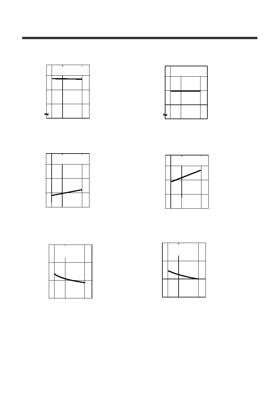
1. DC Characteristics
1.1 Current consumption (READ) I
CC1
vs. ambient temperature Ta
1.2 Current consumption (READ) I
CC1
vs. ambient temperature Ta
Ta (
∞C)
0.4
0.2
V
CC
= 5.5 V
f
SK
= 2 MHz
DATA
= 0101
0
-40 0
85
I
CC1
(mA)
Ta (
∞C)
0.4
0.2
V
CC
= 3.3 V
f
SK
= 500 kHz
DATA
= 0101
0
-40 0 85
I
CC1
(mA)
1.3 Current consumption (READ) I
CC1
vs. ambient temperature Ta
1.4 Current consumption (READ) I
CC1
vs. power supply voltage V
CC
I
CC1
(mA)
Ta (
∞C)
0.4
0.2
V
CC
= 1.8 V
f
SK
= 10 kHz
DATA
= 0101
0
-40 0 85
1 MHz
500 kHz
I
CC1
(mA)
0.4
0.2
0
2 3 4 5 6 7
Ta
= 25∞C
f
SK
= 1 MHz, 500 kHz
DATA
= 0101
V
CC
(V)
1.5 Current consumption (READ) I
CC1
vs. power supply voltage V
CC
1.6 Current consumption (READ) I
CC1
vs. Clock frequency f
SK
100 kHz
10 kHz
I
CC1
(mA)
0.4
0.2
0
2 3 4 5 6 7
V
CC
(V)
Ta
= 25∞C
f
SK
= 100 kHz, 10 kHz
DATA
= 0101
I
CC1
(mA)
0.4
0.2
0
V
CC
= 5.0 V
Ta
= 25∞C
1 M 2M 10M
10 k 100 k
f
SK
(Hz)

CMOS SERIAL E
2
PROM
Rev.2.0
_00
S-93C76A
Seiko Instruments Inc.
15
1.7 Current consumption (WRITE) I
CC2
vs. ambient temperature Ta
1.8 Current consumption (WRITE) I
CC2
vs. ambient temperature Ta
Ta (
∞C)
1.0
0.5
V
CC
= 5.5 V
0
-40 0 85
I
CC2
(mA)
I
CC2
(mA)
Ta (
∞C)
1.0
0.5
V
CC
= 3.3 V
0
-40 0 85
1.9 Current consumption (WRITE) I
CC2
vs. ambient temperature Ta
1.10 Current consumption (WRITE) I
CC2
vs. power supply voltage V
CC
Ta (
∞C)
1.0
0.5
V
CC
= 2.7 V
0
-40 0 85
I
CC2
(mA)
1.0
0.5
0
2 3 4 5 6 7
Ta
= 25∞C
V
CC
(V)
I
CC2
(mA)
1.11 Current consumption in standby mode I
SB
vs. ambient temperature Ta
1.12 Current consumption in standby mode I
SB
vs. power supply voltage V
CC
Ta (∞C)
1.0
0.5
V
CC
= 5.5 V
CS
= GND
0
-40 0
85
I
SB
(
µA)
I
SB
(
µA)
1.0
0.5
0
2 3 4 5 6 7
Ta
= 25∞C
CS
= GND
V
CC
(V)

CMOS SERIAL E
2
PROM
S-93C76A
Rev.2.0
_00
Seiko Instruments Inc.
16
1.13 Input leakage current I
LI
vs. ambient temperature Ta
1.14 Input leakage current I
L1
vs. ambient temperature Ta
1.0
0.5
V
CC
= 5.5 V
CS, SK, DI,
TEST
= 0 V
0
-40
0 85
I
LI
(
µA)
Ta (
∞C)
Ta (
∞C)
1.0
0.5
0
-40 0 85
V
CC
= 5.5 V
CS, SK, DI,
TEST
= 5.5 V
I
LI
(
µA)
1.15 Output leakage current I
LO
vs. ambient temperature Ta
1.16 Output leakage current I
LO
vs. ambient temperature Ta
Ta (
∞C)
1.0
0.5
V
CC
= 5.5 V
DO
= 0 V
0
-40 0 85
I
LO
(
µA)
Ta (∞C)
1.0
0.5
V
CC
= 5.5 V
DO
= 5.5 V
0
-40 0 85
I
LO
(
µA)
1.17 High-level output voltage V
OH
vs. ambient temperature Ta
1.18 High-level output voltage V
OH
vs. ambient temperature Ta
Ta (
∞C)
4.6
4.4
V
CC
= 4.5 V
I
OH
= -400 µA
-40 0 85
V
OH
(V)
4.2
Ta (
∞C)
2.7
2.6
V
CC
= 2.7 V
I
OH
= -100 µA
-40 0 85
V
OH
(V)
2.5
CMOS SERIAL E
2
PROM
Rev.2.0
_00
S-93C76A
Seiko Instruments Inc.
17
1.19 High-level output voltage V
OH
vs. ambient temperature Ta
1.20 High-level output voltage V
OH
vs. ambient temperature Ta
Ta (
∞C)
2.5
2.4
V
CC
= 2.5 V
I
OH
= -100 µA
-40 0
85
V
OH
(V)
2.3
Ta (
∞C)
1.9
1.8
V
CC
= 1.8 V
I
OH
= -10
µ
A
-40 0 85
V
OH
(V)
1.7
1.21 Low-level output voltage V
OL
vs. ambient temperature Ta
1.22 Low-level output voltage V
OL
vs. ambient temperature Ta
Ta (
∞C)
0.3
0.2
V
CC
= 4.5 V
I
OL
= 2.1 mA
-40 0 85
V
OL
(V)
0.1
Ta (
∞C)
0.03
0.02
V
CC
= 1.8 V
I
OL
= 100 µA
-40 0 85
V
OL
(V)
0.01
1.23 High-level output current I
OH
vs. ambient temperature Ta
1.24 High-level output current I
OH
vs. ambient temperature Ta
Ta (
∞C)
-20.0
-10.0
V
CC
= 4.5 V
V
OH
= 2.4 V
0
-40 0 85
I
OH
(mA)
Ta (
∞C)
-2
-1
V
CC
= 2.7 V
V
OH
= 2.4 V
0
-40 0 85
I
OH
(mA)

CMOS SERIAL E
2
PROM
S-93C76A
Rev.2.0
_00
Seiko Instruments Inc.
18
1.25 High-level output current I
OH
vs. ambient temperature Ta
1.26 High-level output current I
OH
vs. ambient temperature Ta
Ta (
∞C)
-2
-1
V
CC
= 2.5 V
V
OH
= 2.2 V
0
-40
0 85
I
OH
(mA)
Ta (
∞C)
-1.0
-0.5
V
CC
= 1.8 V
V
OH
= 1.6 V
0
-40 0 85
I
OH
(mA)
1.27 Low-level output current I
OL
vs. ambient temperature Ta
1.28 Low-level output current I
OL
vs. ambient temperature Ta
Ta (
∞C)
20
10
V
CC
= 4.5 V
V
OL
= 0.4 V
0
-40 0
85
I
OL
(mA)
Ta (
∞C)
1.0
0.5
V
CC
= 1.8 V
V
OL
= 0.1 V
0
-40 0
85
I
OL
(mA)
1.29 Input inverted voltage V
INV
vs. power supply voltage V
CC
1.30 Input inverted voltage V
INV
vs. ambient temperature Ta
3.0
1.5
0
1 2 3 4 5 6
Ta
= 25∞C
CS, SK, DI
V
CC
(V)
V
INV
(V)
7
Ta (
∞C)
3.0
2.0
V
CC
= 5.0 V
CS, SK, DI
0
-40 0
85
V
INV
(V)

CMOS SERIAL E
2
PROM
Rev.2.0
_00
S-93C76A
Seiko Instruments Inc.
19
1.31 Low supply voltage detection voltage
-
-
-
-V
DET
vs. ambient temperature Ta
1.32 Low supply voltage release voltage
+
+
+
+V
DET
vs. ambient temperature Ta
Ta (
∞C)
2.0
1.0
0
-40 0 85
-V
DET
(V)
Ta (
∞C)
2.0
1.0
0
-40 0 85
+V
DET
(V)
2. AC Characteristics
2.1 Maximum operating frequency f
max
vs. power supply voltage V
CC
2.2 Write time t
PR
vs. power supply voltage V
CC
10k
2 3 4 5
Ta
= 25∞C
V
CC
(V)
f
max.
(Hz)
1
100k
1M
2M
4
2
2 3 4 5 6 7
Ta
= 25∞C
V
CC
(V)
t
PR
(ms)
1
2.3 Write time t
PR
vs. ambient temperature Ta
2.4 Write time t
PR
vs. ambient temperature Ta
Ta (
∞C)
6
4
V
CC
= 5.0 V
-40 0 85
2
t
PR
(ms)
Ta (
∞C)
6
4
V
CC
= 3.0 V
-40 0 85
2
t
PR
(ms)

CMOS SERIAL E
2
PROM
S-93C76A
Rev.2.0
_00
Seiko Instruments Inc.
20
2.5 Write time t
PR
vs. ambient temperature Ta
2.6 Data output delay time t
PD
vs. ambient temperature Ta
Ta (
∞C)
6
4
V
CC
= 2.7 V
-40 0 85
2
t
PR
(ms)
Ta (
∞C)
0.3
0.2
V
CC
= 4.5 V
-40 0 85
0.1
t
PD
(
µs)
2.7 Data output delay time t
PD
vs. ambient temperature Ta
2.8 Data output delay time t
PD
vs. ambient temperature Ta
Ta (
∞C)
0.6
0.4
V
CC
= 2.7 V
-40 0 85
0.2
t
PD
(
µs)
Ta (
∞C)
1.5
1.0
V
CC
= 1.8 V
-40 0 85
0.5
t
PD
(
µs)

CMOS SERIAL E
2
PROM
Rev.2.0
_00
S-93C76A
Seiko Instruments Inc.
21
Product Code Structure
Operation temperature
none:
-40 to +85∞C
H:
-40 to +105∞C (Only 8-Pin SOP(JEDEC))
IC direction in tape specification (Except 8-Pin DIP)
Package name (abbreviation) and IC packing specifications
DP: 8-Pin
DIP
DFJ:
8-Pin
SOP(JEDEC)
FT: 8-Pin
TSSOP
Product name
S-93C76A : 8k bit
S-93C76A xxx
- TB x

No.
TITLE
SCALE
UNIT
mm
Seiko Instruments Inc.
DIP8-F-PKG Dimensions
No. DP008-F-P-SD-1.1
DP008-F-P-SD-1.1
0.48±0.1
2.54
0.89
1.3
0∞ to 15∞
0.25
+0.11
-0.05
7.62
9.6(10.6max.)
1
4
5
8
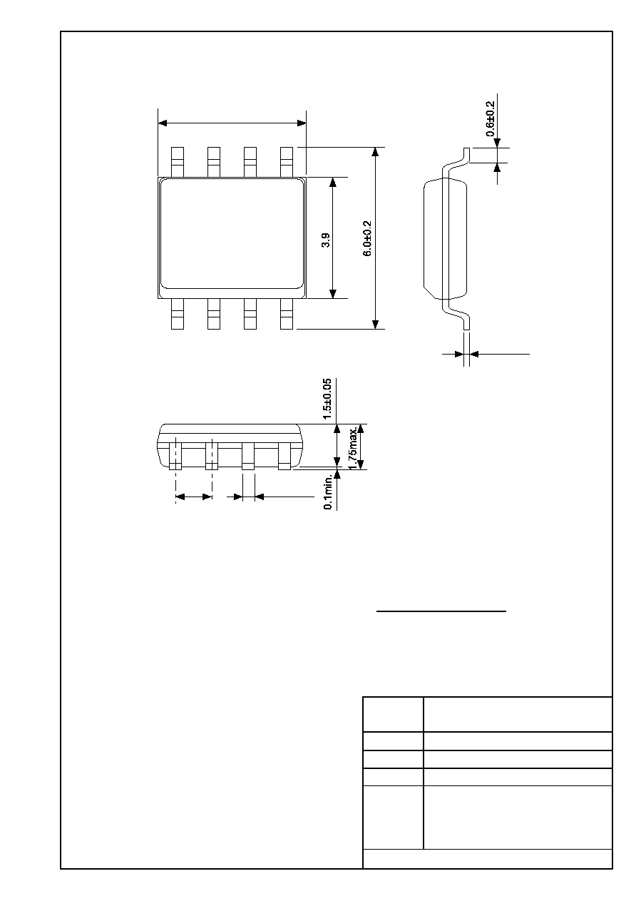
No. FJ008-A-P-SD-2.1
0.4±0.05
1.27
0.20±0.05
5.02±0.2
1
4
8
5
No.
TITLE
SCALE
UNIT
mm
SOP8J-A-PKG Dimensions
Seiko Instruments Inc.
FJ008-A-P-SD-2.1

No.
TITLE
SCALE
UNIT
mm
5
8
1
4
¯2.0±0.05
¯1.55±0.05
0.3±0.05
2.1±0.1
8.0±0.1
5∞max.
6.7±0.1
2.0±0.05
Seiko Instruments Inc.
Feed direction
4.0±0.1(10 pitches:40.0±0.2)
SOP8J-D-Carrier Tape
No. FJ008-D-C-SD-1.1
FJ008-D-C-SD-1.1

No.
TITLE
SCALE
UNIT
mm
QTY.
2,000
2±0.5
13.5±0.5
60∞
2±0.5
¯13±0.2
¯21±0.8
Seiko Instruments Inc.
Enlarged drawing in the central part
SOP8J-D-Reel
No. FJ008-D-R-SD-1.1
FJ008-D-R-SD-1.1

No.
TITLE
SCALE
UNIT
mm
Seiko Instruments Inc.
0.17±0.05
3.00
+0.3
-0.2
0.65
0.2±0.1
1
4
5
8
TSSOP8-A-PKG Dimensions
No. FT008-A-P-SD-1.1
FT008-A-P-SD-1.1

No.
TITLE
SCALE
UNIT
mm
Seiko Instruments Inc.
¯1.5
2.0±0.05
8.0±0.1
¯1.5
+0.1
-0
6.9±0.1
4.4±0.2
0.3±0.05
1
4
5
8
4.0±0.1
Feed direction
TSSOP8-D-Carrier Tape
No. FT008-D-C-SD-1.0
FT008-D-C-SD-1.0
+0.1
-0

No.
TITLE
SCALE
UNIT
mm
Seiko Instruments Inc.
QTY.
3,000
Enlarged drawing in the central part
TSSOP8-D-Reel
No. FT008-D-R-SD-1.0
FT008-D-R-SD-1.0
2±0.5
13.5±0.5
60∞
2±0.5
¯13±0.2
¯21±0.8

∑
The information described herein is subject to change without notice.
∑
Seiko Instruments Inc. is not responsible for any problems caused by circuits or diagrams described herein
whose related industrial properties, patents, or other rights belong to third parties. The application circuit
examples explain typical applications of the products, and do not guarantee the success of any specific
mass-production design.
∑
When the products described herein are regulated products subject to the Wassenaar Arrangement or other
agreements, they may not be exported without authorization from the appropriate governmental authority.
∑
Use of the information described herein for other purposes and/or reproduction or copying without the
express permission of Seiko Instruments Inc. is strictly prohibited.
∑
The products described herein cannot be used as part of any device or equipment affecting the human
body, such as exercise equipment, medical equipment, security systems, gas equipment, or any apparatus
installed in airplanes and other vehicles, without prior written permission of Seiko Instruments Inc.
∑
Although Seiko Instruments Inc. exerts the greatest possible effort to ensure high quality and reliability, the
failure or malfunction of semiconductor products may occur. The user of these products should therefore
give thorough consideration to safety design, including redundancy, fire-prevention measures, and
malfunction prevention, to prevent any accidents, fires, or community damage that may ensue.